 | ÐлекÑÑоннÑй компоненÑ: AD5934 | СкаÑаÑÑ:  PDF PDF  ZIP ZIP |
AD5934 250 kSPS 12-Bit Impedance Converter Network Analyzer Data Sheet (Rev. PrA)
250KSPS 12 Bit Impedance Converter
Network Analyzer
Preliminary Technical Data
AD5934
Rev. PrA
Information furnished by Analog Devices is believed to be accurate and reliable.
However, no responsibility is assumed by Analog Devices for its use, nor for any
infringements of patents or other rights of third parties that may result from its use.
Specifications subject to change without notice. No license is granted by implication
or otherwise under any patent or patent rights of Analog Devices. Trademarks and
registered trademarks are the property of their respective owners.
One Technology Way, P.O. Box 9106, Norwood, MA 02062-9106, U.S.A.
Tel: 781.329.4700
www.analog.com
Fax: 781.326.8703
© 2004 Analog Devices, Inc. All rights reserved.
FEATURES
50KHz Max Excitation Output
Impedance Range .1k 20M Ohm, 12-Bit Resolution
System Clock provided via MCLK pin
DSP Real and Imaginary Calculation (FFT)
3V Power Supply, Programmable Sinewave Output
Frequency Resolution 27 Bits (<0.1 Hz)
Frequency Sweep Capability
12-Bit Sampling ADC
ADC Sampling 250KSPS, INL ± 1LSB Max
Serial I
2
C Loading
Temperature Range -40 125°C
16 SSOP
APPLICATIONS
Complex Impedance Measurement
Impedance Spectrometry
Biomedical and Automotive Sensors
Proximity Sensors
FFT Processing
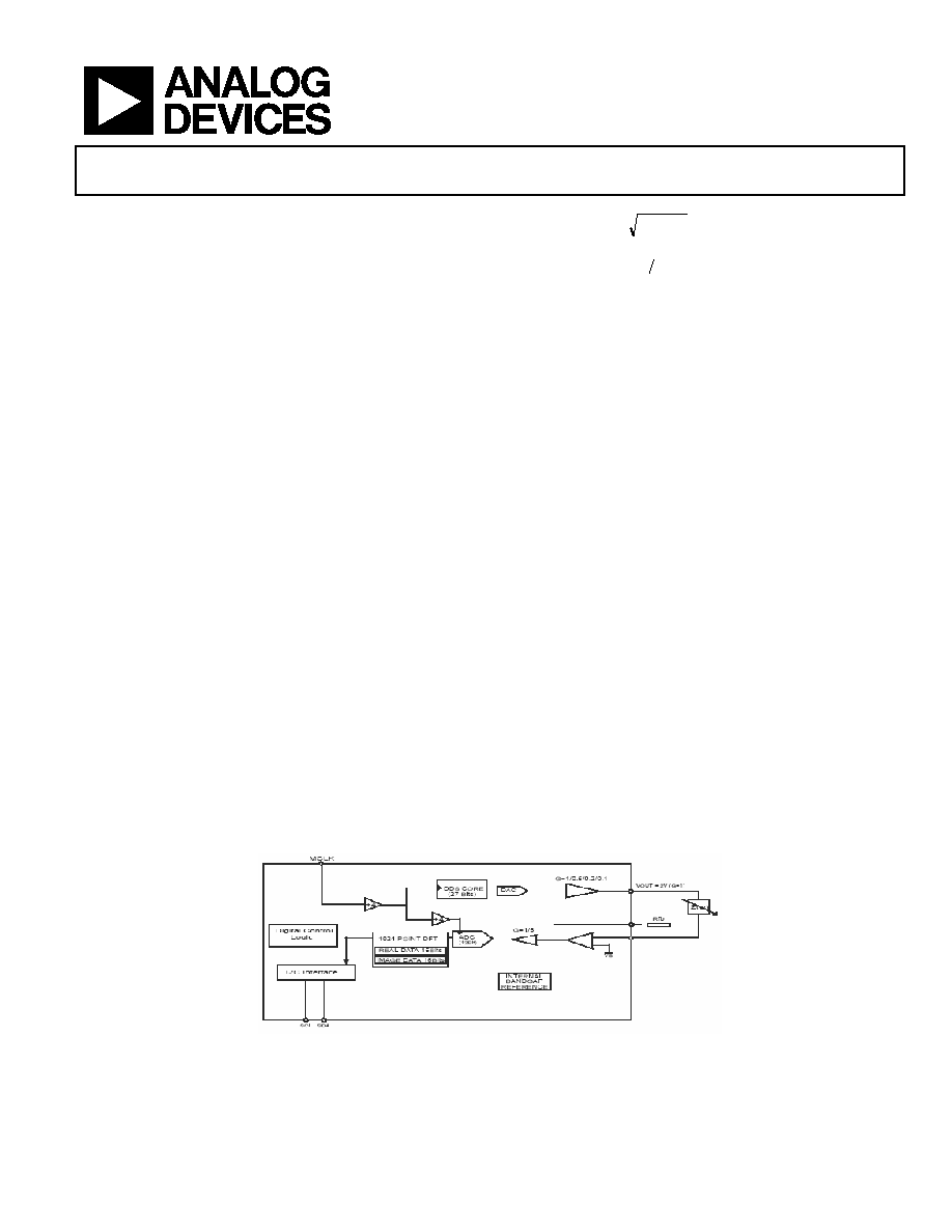
GENERAL DESCRIPTION
The AD5934 is a high precision impedance converter system
solution which combines an on-board frequency generator with
a 12-bit 250KSPS ADC. The frequency generator allows an
external complex impedance to be excited with a known
frequency. The response signal from the impedance is sampled
by the onboard ADC and FFT processed by an onboard DSP
engine. The FFT algorithm returns a Real (R) and Imaginary (I)
data word, allowing impedance to be conveniently calculated.
The impedance magnitude and phase is easily calculated using
the following equations:
2
2
I
R
Magnitude
+
=
( )
R
I
Tan
Phase
1
-
=
To determine the actual real impedance value Z(W), a
frequency sweep is generally performed. The impedance can be
calculated at each point, and a frequency vs. magnitude plot can
be created.
The system allows the user to program a 2 V PK-PK sinusoidal
signal as excitation to an external load. Output ranges of 1 V,
500 mV, and 200 mV can also be programmed. The signal is
provided on chips using DDS techniques. Frequency resolution
of 27 bits (less than 0.1HZ) can be achieved.
To perform the frequency sweep, the user must first program
the conditions required for the sweep; start frequency, delta
frequency, step frequency, etc. A Start Command is then
required to begin the sweep.
At each point on the sweep the, ADC takes 1024 samples and
calculates a Discrete Fourier Transform to provide the real and
imaginary data for the waveform. The real and imaginary data
is available to the user through the 12C interface.
To determine the impedance of the load at any one frequency
point, Z(w), a measurement system comprised of a trans
impedance amplifier, gain stage, and ADC are used to record
data. The gain stage for the response stage is 1 or 5.
The ADC is a low-noise, high-speed 250 KSPS sampling ADC
that operates from a 3 V supply. Clocking for both the DDS and
ADC signals is provided externally via the MCLK reference
clock, which is provided externally from a crystal oscillator. The
AD5934 is available in a 16 ld SSOP.
Figure 1.

AD5934
Preliminary Technical Data
Rev. PrA | Page 2 of 20
TABLE OF CONTENTS
Specifications..................................................................................... 3
Timing Characteristics..................................................................... 5
Pin Configuration and Function Descriptions............................. 6
General Description ......................................................................... 7
Output Stage.................................................................................. 7
Circuit Description....................................................................... 7
Sin Rom.......................................................................................... 8
Response Stage.............................................................................. 8
ADC Operation ............................................................................ 8
DFT Conversion ........................................................................... 9
Register Map.................................................................................... 10
Control Register.......................................................................... 11
Control Register Map................................................................. 11
Control Register Decode ........................................................... 12
Reset ............................................................................................. 12
System Clock............................................................................... 12
Output Voltage............................................................................ 12
Post Gain ..................................................................................... 12
Serial Bus Interface..................................................................... 13
General I2C Timing ................................................................... 13
Writing/Reading to the AD5934 .......................................... 14
Write Byte/Command Byte....................................................... 14
Block Write.................................................................................. 15
Read Operations......................................................................... 15
P.E.C. ............................................................................................ 16
Checksum.................................................................................... 16
Outline Dimensions ....................................................................... 17
ESD Caution................................................................................ 17
REVISION HISTORY
12/04--Revision PrA Preliminary Version

Preliminary Technical Data
AD5934
Rev. PrA | Page 3 of 20
SPECIFICATIONS
VDD = +3.0 V ± 10%. TMIN to TMAX unless otherwise noted.
Table 1.
B
Version
1
Parameter Min
Typ
Max
Unit
Test
Conditions/Comments
System Specs
Impedance Range
.0001
20
M Ohm
Total System Accuracy
1
%
System ppm
TDB
ppm/°C
MCLK Update Rate
16
MSPS
Output Stage
Frequency Specs
Output Frequency Range
0
50KHz
Hz
Uni-polar sinusoidal signal
Frequency Resoltuion
27
Bits
<0.1 Hz resolution
MCLK
External reference clock; typically 16.667 MHz
Initial Frequency Accuracy
0.1
Hz
Output excitation accuracy. 0 -50 KHz range
Output Voltage Specs
AC Voltage Range
2.0
Volts
Pk-Pk unipolar voltage on output
Output Voltage Error
TBD
%
Voltage error on Pk-Pk output
DC Bias
Vdd/2
Volts
DC bias of AC signal
DC Bias Error
TBD
%
Tolerance of DC bias
AC Voltage Range
1.0
Volts
Pk-Pk unipolar voltage on output
Output Voltage Error
TBD
%
Voltage error on Pk-Pk output
DC Bias
Vdd/4
Volts
DC bias of AC signal
DC Bias Error
±1
%
Tolerance of DC bias
AC Voltage Range
0.4
Volts
Pk-Pk unipolar voltage on output
Output Voltage Error
TBD
%
Voltage error on Pk-Pk output
DC Bias
Vdd/8
Volts
DC bias of AC signal
DC Bias Error
TBD
%
Tolerance of DC Bias
AC Voltage Range
0.2
Volts
Pk-Pk unipolar voltage on output
Output Voltage Error
TBD
%
Voltage error on Pk-Pk output
DC Bias
Vdd/16
Volts
DC bias of AC signal
DC Bias Error
TBD
%
Tolerance of DC bias
DC Output Impedance
120
Ohm
Short Circuit Current
75
mA
At 3 volts
Short Circuit Current
100
mA
At 5 volts
AC Characteristics
Signal to Noise Ratio
60
db
Total Harmonic Distortion
-66
db
Spurious free Dynamic Range
Wideband
60
db
Narrowband
80
db
Clock Feedthrough
TBD
db

AD5934
Preliminary Technical Data
Rev. PrA | Page 4 of 20
B
Version
1
Parameter Min
Typ
Max
Unit
Test
Conditions/Comments
System Response Stage
Analog Input VIN
Input Leakage Current
1
nA
To Pin VIN
Input Capacitance
0.5
pF
To Pin VIN
Input Impedance
100M
Ohm
To Pin VIN
ADC Accuracy
Resolution
12
Sampling Rate
1
MSPS
Integral Nonlinearity
±1
LSB
No missing codes
Differential Nonlinearity
±1
LSB
Offset Error
Gain Error
TEMPERATURE SENSOR
Accuracy
±2
°C
TA = -40 125 degrees
Resolution
0.03125
°C
Temperature Conversion Time
TBD
µS
LOGIC INPUTS
Vih, Input High Voltage
2.2
VDD = 3v
Vil, Input Low Voltage
0.8
VDD = 3V
Input Current
±1
µA
Input Capacitance
±3
pF
POWER REQUIREMENTS
Vdd
3.0
Volts
IDD (Normal Mode)
15
mA
IDD (Powerdown Mode)
TBD
µA
1
Temperature ranges are as follows: B Version: -40°C to +125°C, typical at 25°C.
2
Guaranteed by design and characterization, not production tested.
Preliminary Technical Data
AD5934
Rev. PrA | Page 5 of 20
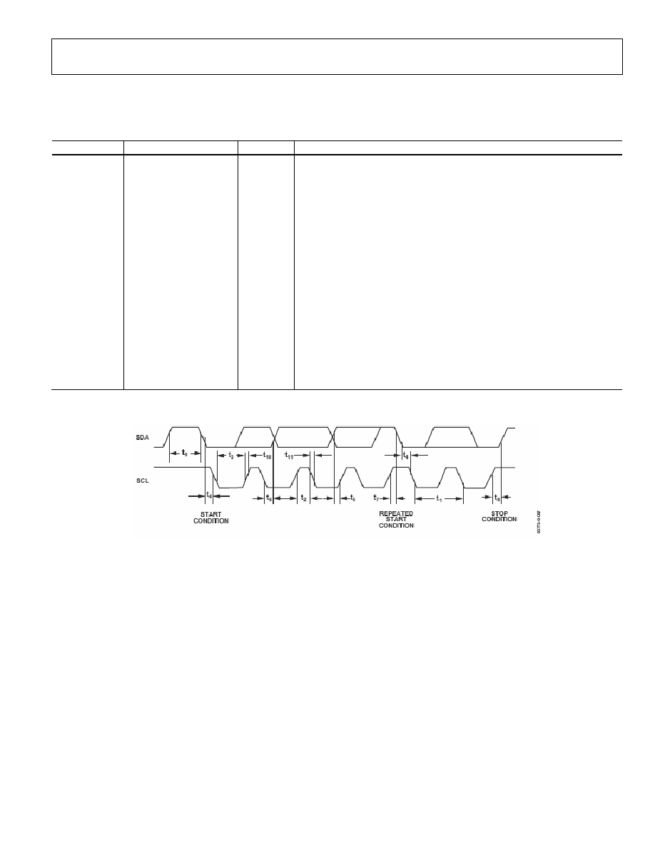
TIMING CHARACTERISTICS
Table 2. I
2
C Serial Interface
Parameter
Limit at T
MIN
, T
MAX
Unit Description
F
SCL
400
kHz max
SCL clock frequency
t
1
2.5
µs min
SCL cycle time
t
2
0.6
µs
min
t
HIGH
, SCL high time
t
3
1.3
µs
min
t
LOW
, SCL low time
t
4
0.6
µs
min
t
HD, STA
, start/repeated start condition hold time
t
5
100
ns
min
t
SU, DAT
, data setup time
t
6
0.9
µs
max
t
HD, DAT
, data hold time
0
µs
min
t
HD, DAT
, data hold time
t
7
0.6
µs
min
t
SU, STA
, setup time for repeated start
t
8
0.6
µs
min
t
SU, STO
, stop condition setup time
t
9
1.3
µs
min
t
BUF
, bus free time between a stop and a start condition
t
10
300
ns
max
t
F
, fall time of SDA when transmitting
0
ns
min
t
R
, rise time of SCL and SDA when receiving (CMOS compatible)
t
11
300
ns
max
t
F
, fall time of SDA when transmitting
0
ns
min
t
F
, fall time of SDA when receiving (CMOS compatible)
300
ns
max
t
F
, fall time of SCL and SDA when receiving
20 + 0.1 C
B
ns
min
t
F
, fall time of SCL and SDA when transmitting
C
B
400
pF max
Capacitive load for each bus line
Figure 2. I
2
C Interface Timing Diagram
Document Outline