 | –≠–ª–µ–∫—Ç—Ä–æ–Ω–Ω—ã–π –∫–æ–º–ø–æ–Ω–µ–Ω—Ç: AD9959 | –°–∫–∞—á–∞—Ç—å:  PDF PDF  ZIP ZIP |
4 Channel 500MSPS DDS with 10-bit DACs
Preliminary Technical Data
AD9959
Rev. PrB
Information furnished by Analog Devices is believed to be accurate and reliable.
However, no responsibility is assumed by Analog Devices for its use, nor for any
infringements of patents or other rights of third parties that may result from its use.
Specifications subject to change without notice. No license is granted by implication
or otherwise under any patent or patent rights of Analog Devices. Trademarks and
registered trademarks are the property of their respective owners.
One Technology Way, P.O. Box 9106, Norwood, MA 02062-9106, U.S.A.
Tel: 781.329.4700
www.analog.com
Fax: 781.326.8703
© 2004 Analog Devices, Inc. All rights reserved.
FEATURES
Four synchronized DDS channels @500 MSPS
Independent frequency / phase / amplitude
control between all channels
Matched latencies for Freq, Phase, and Amplitude changes
Excellent channel to channel isolation
Frequency sweeping capability
Up to 16 levels of modulation (pin selectable)
Individually programmable DAC full scale currents
Four integrated 10-bit D/A converters(DACs)
32-bit frequency tuning resolution
14-bit phase offset resolution
10-bit output amplitude scaling resolution
Serial I/O Port(SPI) with enhanced data throughput
Software/Hardware controlled power-down
Dual supply operation (1.8 V DDS core / 3.3 V serial I/O)
Built-in synchronization for multiple devices
Selectable REF_CLK multipier(PLL) 4x to 20x (bypassable)
Selectable REF_CLK crystal operation
56 pin LFCSP package
APPLICATIONS
Agile L.O. frequency synthesis
Phased array radar / sonar
Instrumentation
Synchronized clocking
RF source for AOTF
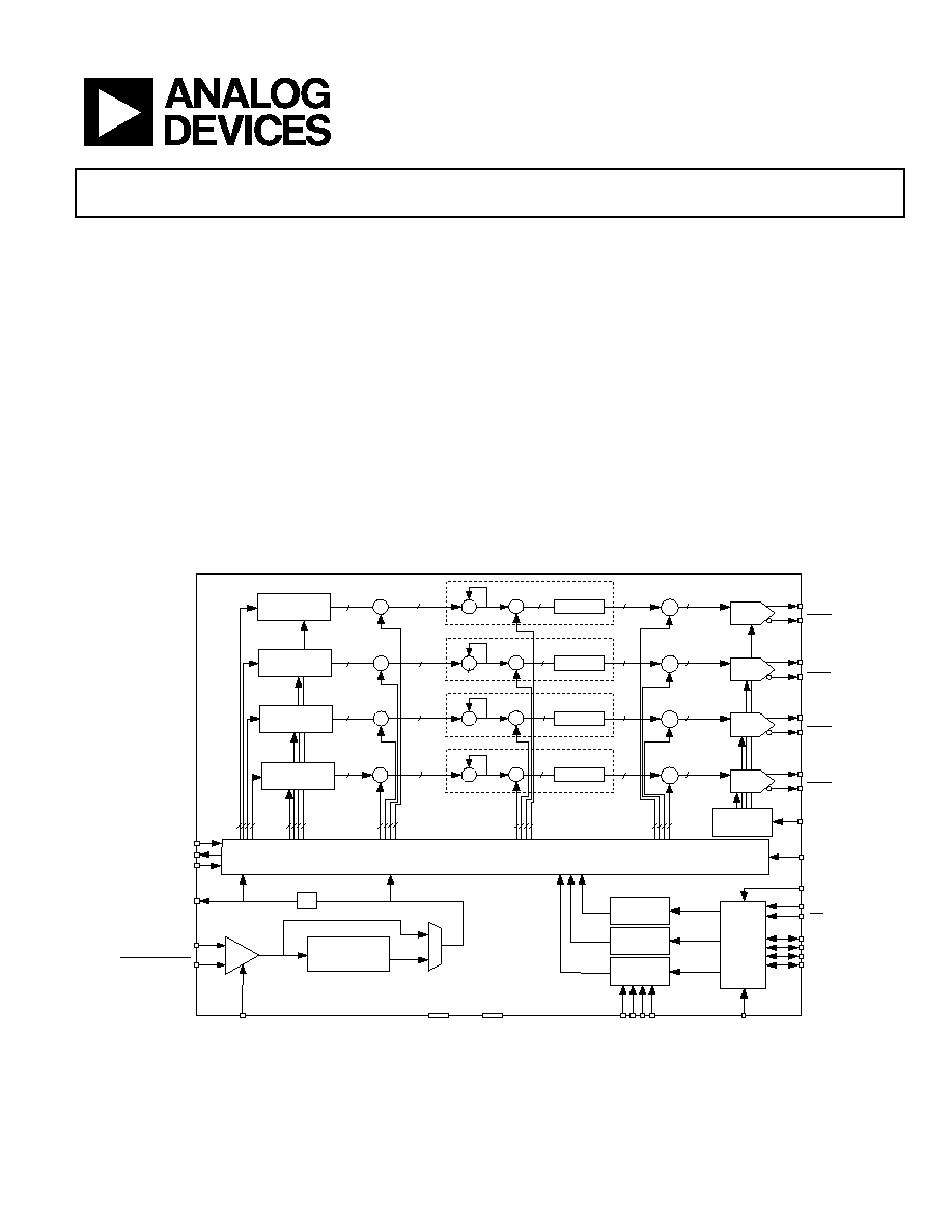
FUNCTIONAL BLOCK DIAGRAM
14
BUFFER / XTAL
OSCILLATOR
CLK_MODE_SEL
M
U
X
REF CLOCK
MULTIPLIER
(PLL) 4x to 20x
CHANNEL
REGISTERS
PWR_DWN_CTL
FTW
PHASE
OFFSET
IOUT
DAC
˜4
OSC / REF_CLK
MASTER_RESET
CS
SCLK
SDIO_0
SDIO_1
SDIO_2
SDIO_3
SCALABLE
DAC REF
CURRENT
DAC_RSET
COS(X)
DIGITAL
MULTIPLIER
I/O
Port
Buffer
◊
10
FREQUENCY
ACCUMULATOR
10
10
DAC
COS(X)
◊
10
10
DAC
COS(X)
◊
10
10
DAC
COS(X)
◊
10
10
32
8
RAMP
RATE
DFTW
32
Timing & Control Logic
SYNC_CLK
SYNC_IN
SYNC_OUT
PROFILE
REGISTERS
P
S
0
P
S
3
P
S
2
P
S
1
SYSTEM
CLK
I/O_UPDATE
AVDD
DVDD
DVDD_IO
1.8V
1.8V
3.3V
15
32
32
32
32
32
32
32
32
15
15
15
OSC / REF_CLK
DDS CORE
DDS CORE
DDS CORE
DDS CORE
CONTROL
REGISTERS
IOUT
IOUT
IOUT
IOUT
IOUT
IOUT
IOUT
FREQUENCY
ACCUMULATOR
FREQUENCY
ACCUMULATOR
FREQUENCY
ACCUMULATOR
Figure 1 AD9959 Block Diagram

AD9959
Preliminary Technical Data
Rev. PrB | Page 2 of 9
AD9959--SPECIFICATIONS
Table 1. Unless otherwise noted, AVDD,
DVDD = 1.8 V ± 5%, DVDD_I/O = 3.3 V ± 5%, R
SET
= 1.96 k, External Reference Clock
Frequency = 500 MSPS (REF_CLK multiplier bypassed)
Parameter
Min
Typ
Max
Units
Test Conditions/Comments
REF CLOCK INPUT CHARACTERISTICS
REF_CLK inputs must be AC
coupled due to internal biasing
Frequency Range
REF_CLK Multiplier bypassed
0
500
MHz
REF_CLK Multiplier enabled at 4x(min)
25
125
MHz
REF_CLK Multiplier enabled at 20x(max)
5
25
MHz
Internal VCO range w/ REF_CLK multiplier enabled
100
500
MHz
Crystal REF_CLK source mode
20
30
MHz
Input Power Sensitivity
-15
3
dBm
External 50 ohm termination
Input voltage level
400
mV
Input Capacitance
3
pF
Input Impedance
1500
ohms
Duty Cycle w/ REF_CLK Multiplier bypassed
50
%
Duty Cycle w/ REF_CLK Multiplier enabled
35
65
%
CLK Mode Select logic 1 Voltage
1.25
V
Not a 3.3V digital input
CLK Mode Select logic 0 Voltage
0.6
V
Not a 3.3V digital input
DAC OUTPUT CHARACTERISTICS
Must be referenced to AVDD
Resolution
10
Bits
Full Scale Ouput Current
10
mA
Gain Error
-10
10
%FS
Output Offset
0.6
uA
Differential Nonlinearity
-0.5
0.5
LSB
Integral Nonlinearity
-1
1
LSB
Output Capactiance
5 pF
Voltage Compliance Range
AVDD≠
0.50
AVDD
+ 0.50
V
Channel to Channel Isolation
60
dB
Channel to Channel amplitude matching error
2
%
WIDEBAND SFDR
Wideband SFDR defined as DC to
Nyquist
1-20 MHz Analog Out
-65
dBc
20-60 MHz Analog Out
-62
dBc
60-100 MHz Analog Out
-59
dBc
100-150 MHz Analog Out
-56
dBc
150-200 MHz Analog Out
-54
dBc
NARROWBAND SFDR
1.1 MHz Analog Out (+/- 10kHz)
-90
dBc
1.1 MHz Analog Out (+/- 50kHz)
-88
dBc
1.1 MHz Analog Out (+/- 250kHz)
-86
dBc
1.1 MHz Analog Out (+/- 1MHz)
-85
dBc
15.1 MHz Analog Out (+/- 10kHz)
-90
dBc
15.1 MHz Analog Out (+/- 50kHz)
-87
dBc
15.1 MHz Analog Out (+/- 250kHz)
-85
dBc
15.1 MHz Analog Out (+/- 1MHz)
-83
dBc
40.1 MHz Analog Out (+/- 10kHz)
-90
dBc
40.1 MHz Analog Out (+/- 50kHz)
-87
dBc
40.1 MHz Analog Out (+/- 250kHz)
-84
dBc
40.1 MHz Analog Out (+/- 1MHz)
-82
dBc

Preliminary Technical Data
AD9959
Rev. PrB | Page 3 of 9
Parameter
Min
Typ
Max Units Test
Conditions/Comments
75.1 MHz Analog Out (+/- 10kHz)
-87
dBc
75.1 MHz Analog Out (+/- 50kHz)
-85
dBc
75.1 MHz Analog Out (+/- 250kHz)
-83
dBc
75.1 MHz Analog Out (+/- 1MHz)
-82
dBc
100.1 MHz Analog Out (+/- 10kHz)
-87
dBc
100.1 MHz Analog Out (+/- 50kHz)
-85
dBc
100.1 MHz Analog Out (+/- 250kHz)
-83
dBc
100.1 MHz Analog Out (+/- 1MHz)
-81
dBc
200.1 MHz Analog Out (+/- 10kHz)
-87
dBc
200.1 MHz Analog Out (+/- 50kHz)
-85
dBc
200.1 MHz Analog Out (+/- 250kHz)
-83
dBc
200.1 MHz Analog Out (+/- 1MHz)
-81
dBc
PHASE NOISE CHARACTERISTICS
Residual Phase Noise @15.1 MHz(Aout)
@1kHz offset
TBD
dBc/ Hz
@10kHz offset
TBD
dBc/ Hz
@100kHz offset
TBD
dBc/ Hz
@1MHz offset
TBD
dBc/ Hz
Residual Phase Noise @ 75.1 MHz(Aout)
@1kHz offset
TBD
dBc/ Hz
@10kHz offset
TBD
dBc/ Hz
@100kHz offset
TBD
dBc/ Hz
@1MHz offset
TBD
dBc/ Hz
Residual Phase Noise @ 200.1 MHz(Aout)
@1kHz offset
TBD
dBc/ Hz
@10kHz offset
TBD
dBc/ Hz
@100kHz offset
TBD
dBc/ Hz
@1MHz offset
TBD
dBc/ Hz
Residual Phase Noise @ 15.1 MHz(Aout)
w/ REF CLK multiplier enabled 4x
@1kHz offset
TBD
dBc/ Hz
@10kHz offset
TBD
dBc/ Hz
@100kHz offset
TBD
dBc/ Hz
@1MHz offset
TBD
dBc/ Hz
Residual Phase Noise @ 75.1 MHz(Aout)
w/ REF CLK multiplier enabled 4x
@1kHz offset
TBD
dBc/ Hz
@10kHz offset
TBD
dBc/ Hz
@100kHz offset
TBD
dBc/ Hz
@1MHz offset
TBD
dBc/ Hz
Residual Phase Noise @ 200.1 MHz(Aout)
w/ REF CLK multiplier enabled 4x
@1kHz offset
TBD dBc/
Hz
@10kHz offset
TBD dBc/
Hz
@100kHz offset
TBD dBc/
Hz
@1MHz offset
TBD dBc/
Hz
SERIAL PORT TIMING CHARACTERISTICS
Maximum Frequency
200
MHz
Minimum Clock Pulsewidth Low (t
PWL
)
TBD
ns
Minimum Clock Pulsewidth High (t
PWH
)
TBD
ns

AD9959
Preliminary Technical Data
Rev. PrB | Page 4 of 9
Maximum Clock Rise/Fall Time
TBD
ns
Minimum Data Setup Time (t
DS
)
TBD
ns
Minimum Data Hold Time
TBD
ns
MISC TIMING CHARACTERISTICS
Master_Reset minimum Pulsewidth
TBD
Sync
CLK
I/O_Update minimum Pulsewidth
1
Sync
CLK
Minimum setup time (IO_Update to Sync_CLK)
TBD
ns
Rising edge to rising edge
Minimum hold time (IO_Update to Sync_CLK)
0
ns
Rising edge to rising edge
Minimum setup time (Profile inputs to Sync_CLK)
TBD
ns
Minimum hold time (Profile inputs to Sync_CLK)
0
ns
DATA LATENCY (PIPE LINE DELAY)
Pipeline delays for Freq, Phase,
Amp changes are programmable to
match one another.
Matched pipe line of Freq, Phase, Amplitude
TBD
Sys
Clks
matched
Frequency word to DAC output
TBD
Sys
Clks
unmatched
Phase Offset word to DAC output
TBD
Sys
Clks
unmatched
Amplitude word to DAC output
TBD
Sys
Clks
unmatched
CMOS LOGIC INPUTS
V
IH
2.2
V
V
IL
0.6 V
Logic 1 Current
3
12 uA
Logic 0 Current
-12
uA
Input Capacitance
2
pF
CMOS LOGIC OUTPUTS (1 mA Load)
V
OH
2.8
V
V
OL
0.4 V
POWER SUPPLY
Total Power Dissipation- all channels ON, single-tone mode
TBD
mW
Maximum Power Dissipation- all channels, freq accumulator
output multiplier ON
TBD
Iavdd ≠ All Channels ON, Single tone mode
TBD
mA
Iavdd ≠ All Ch(s) ON, Freq accum, and output multiplier ON
TBD
mA
Idvdd ≠ All Ch(s) ON, Single tone mode
TBD
mA
Idvdd ≠ All Ch(s) ON, Freq accum, and output multiplier ON
TBD
mA
Idvdd_I/O
TBD
mA
Power down Mode
TBD
mA

Preliminary Technical Data
AD9959
Rev. PrB | Page 5 of 9
ABSOLUTE MAXIMUM RATINGS
Table 2.
Parameter Rating
Maximum Junction Temperature
150∞C
DVDD_I/O (Pin 49)
4 V
AVDD, DVDD
2 V
Digital Input Voltage (DVDD_I/O = 3.3 V)
≠0.7 V to +4V
Digital Output Current
5 mA
Storage Temperature
≠65∞C to +150∞C
Operating Temperature
≠40∞C to +105∞C
Lead Temperature (10 sec Soldering)
300∞C
JA
21∞C/W
JC
2∞C/W
Stresses above those listed under Absolute Maximum Ratings may cause permanent damage to the device. This is a stress rating only and
functional operation of the device at these or any other conditions above those indicated in the operational section of this specification is
not implied. Exposure to absolute maximum rating conditions for extended periods may affect device reliability.
Iout
Iout
INPUT
OUTPUT
DVDD_I/O= 3.3V
TERMINATE OUTPUTS
INTO AVDD. DO NOT
EXCEED OUTPUT
VOLTAGE COMPLIANCE.
AVOID OVERDRIVING
DIGITAL INPUTS.
FORWARD BIASING
DIODES MAY COUPLE
DIGITAL NOISE ON
POWER PINS.
1.5 k
1.5 k
REF_CLK
REF_CLK
z z
AVDD
REF_CLK INPUTS ARE
INTERNALLY BIASED AND
NEED TO BE AC-COUPLED.
OSC INPUTS ARE DC
COUPLED
CMOS
DIGITAL
INPUTS
DAC OUPUTS
OSC / REF_CLK
INPUTS
AMP
OSC
OSC
AVDD
AVDD
Figure 1 Equivalent input and output circuits

AD9959
Preliminary Technical Data
Rev. PrB | Page 6 of 9
PRODUCT OVERVIEW
The AD9959 consists of four independently programmable
DDS channels. The AD9959 features independent frequency,
phase, and amplitude control of each channel; this allows for the
correction of imbalances due to analog processing such as
filtering, amplification, or PCB layout related mismatches. The
AD9959 supports frequency sweeping for radar and
instrumentation applications. Since all four channels share a
common system clock, they are inherently synchronized. If
more than four channels are required, synchronizing multiple
AD9959s is a simple task.
The AD9959 uses advanced DDS technology which provides
low power dissipation with high performance. The device
incorporates four integrated high speed 10-bit DACs with
excellent wideband and narrowband SFDR. Each DDS has a 32-
bit frequency tuning word, 14-bits of phase offset, and a 10-bit
output scale multiplier.
Each DAC has it own programmable reference to enable a
different full scale current for each channel.
Each DDS acts as a high resolution frequency divider with the REF_
CLK as the input and the DAC providing the output. The REF_CLK
input source is common to all DDS channels, and can be driven
directly, or used in combination with an integrated REF_CLK
multiplier (using a PLL) up to a maximum of 500 MSPS. The REF_
CLK multiplication factor is programmable from 4 to 20, in integer
steps. The REF_CLK input features an oscillator which supports either
a crystal as a source, or may be bypassed. The crystal frequency must
be between 20MHz and 30MHz. The crystal can be used with or
without the REF_CLK multiplier.
The DAC outputs are supply referenced and must be terminated into
AVDD by a resistor, or an AVDD center-tapped transformer.
The AD9959 comes in a space-saving 56-lead LFCSP package. The
DDS core (AVDD and DVDD pins) must be powered by a 1.8V supply.
The digital I/O interface (SPI) operates at 3.3V and requires that the
pin labeled "DVDD_I/O" (pin 49) be connected to 3.3V.
The AD9959 operates over the industrial temperature range of -40C to
+85
Preliminary Technical Data
AD9959
Rev. PrB | Page 7 of 9
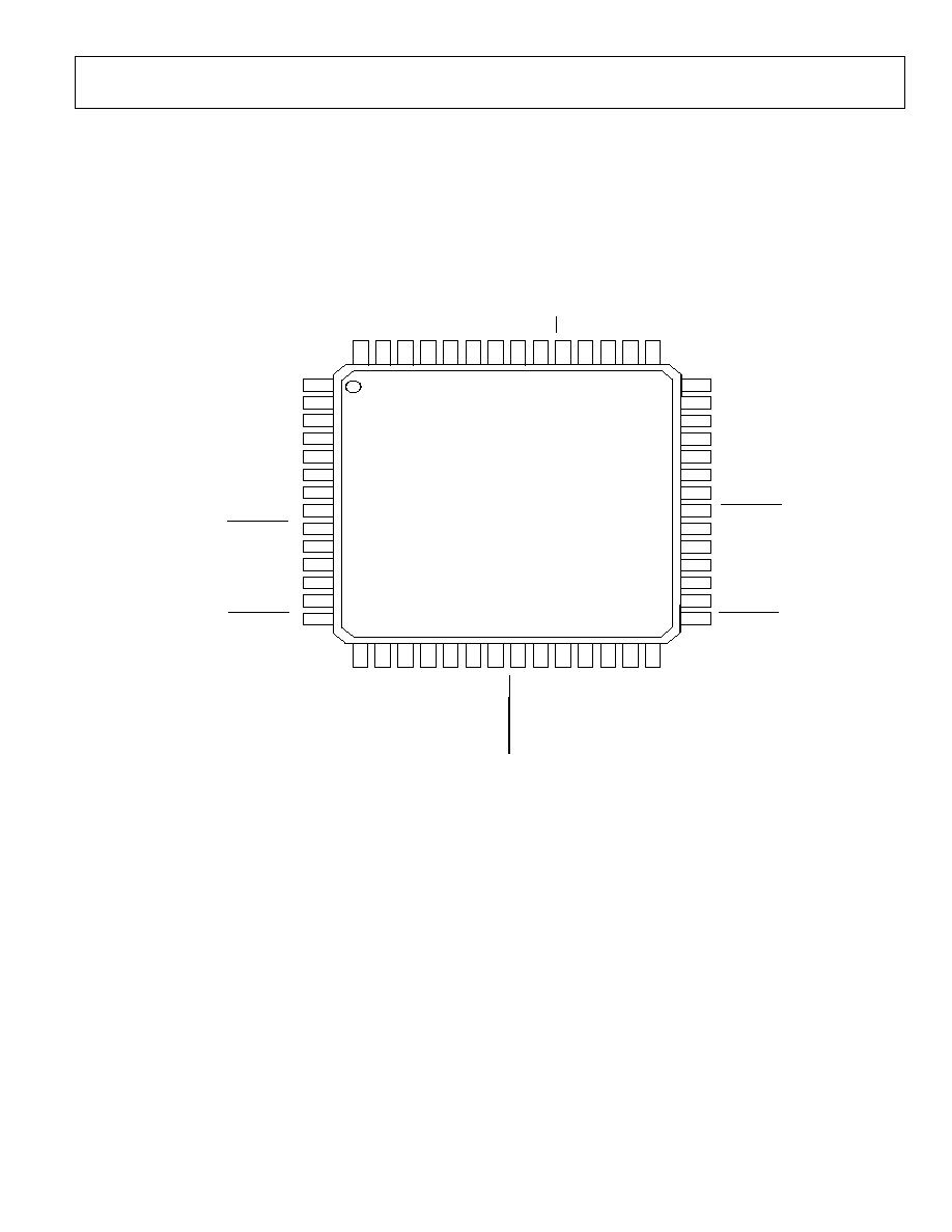
PIN CONFIGURATION
TOP VIEW
(Not to Scale)
17
22
23
24
25
26
27
28
18
19
20
21
16
15
30
31
32
33
34
35
36
37
41
40
39
38
29
42
54
49
DV
DD
DG
ND
48
47
46
45
44
43
53
52
51
50
55
56
CL
K
_
M
O
DE
_
S
E
L
5
4
3
2
11
12
13
AV
D
D
AG
N
D
PWR_DWN_CTL
9
8
7
6
14
1
AG
N
D
AV
D
D
DA
C_
R
S
E
T
AVDD
AVDD
AGND
CH1_IOUT
CH1_IOUT
AVDD
AVDD
CH0_IOUT
CH0_IOUT
AG
N
D
AVDD
AGND
AGND
10
SD
I
O
_
1
SD
I
O
_
2
SD
I
O
_
3
DG
ND
DV
DD
I
/
O
_
U
PD
ATE
SYNC_IN
SYN
C
_
C
L
K
MASTER_RESET
AVDD
AGND
AVDD
CH2_IOUT
CH2 _IOUT
AGND
AGND
CH3_IOUT
CH3_IOUT
AVD
D
AG
N
D
O
S
C /
RE
F
_
C
L
K
OS
C
/
RE
F
_
CL
K
SYNC_OUT
AG
N
D
AV
D
D
LO
O
P
_F
I
L
T
E
R
P0
P1
P2
P3
DV
DD
_
I
/
O
CS
SC
L
K
SD
I
O
_
0
56-LD LFCSP
AD9959
Notes :
1) The exposed EPAD on bottom side of package is an electrical connection and must be
soldered to ground.
2) Pin 49 is DVDD_IO and is tied to 3.3V.

AD9959
Preliminary Technical Data
Rev. PrB | Page 8 of 9
Table 3. Pin Function Descriptions
Pin No.
Mnemonic
I/O
Description
1
SYNC_IN
I
Used to synchronize multiple AD9959s. Connect to the SYNC_OUT pin of the master AD9959.
2
SYNC_OUT
O
Used to synchronize multiple AD9959s. Connect to the SYNC_IN pin of the slave AD9959.
3
MASTER_RESET
I
Active high reset pin. Asserting the RESET pin forces the AD9959's internal registers to their
default state, as described in the serial I/O port register map section in this document.
4 PWR_DWN_CTL
I
External Power-Down Control.
5,7,11,15,19,21,
26,31,33,37,39
AVDD
I
Analog Power Supply Pins (1.8V).
6,10,12,16,18,20,
25,28,32,34,38
AGND
I
Analog Ground Pins.
45, 55
DVDD
I
Digital Power Supply Pins (1.8 V).
44, 56
DGND
I
Digital Power Ground Pins.
8
CH2_IOUT
O
True DAC Output. Terminate into AVDD.
9
_________
CH2_IOUT
O
Complementary DAC Output. Terminate into AVDD.
13
CH3_IOUT
O
True DAC Output. Terminate into AVDD.
14
_________
CH3_IOUT
O
Complementary DAC Output. Terminate into AVDD.
17 DAC_RSET
I
Establishes the reference current for all DACs. A 1.962 k resistor (nominal) is connected from
pin 17 to AGND.
22
OSC / REF_CLK
I
Complementary Reference Clock/Oscillator Input. When the REF_CLK is operated in single-
ended mode, this pin should be decoupled to AVDD or AGND with a 0.1 µF capacitor.
23
OSC / REF_CLK
I
Reference Clock/Oscillator Input. When the REF_CLK is operated in single-ended mode, this is
the input.
24 CLK_MODE_SEL
I
Control Pin for the Oscillator Section. When high (1.8V), the oscillator section is enabled to
accept a crystal as the REFCLK source. When low, the oscillator section is bypassed.
CAUTION: Do not drive this pin beyond 1.8V.
27 LOOP_FILTER
I
Connect to the external zero compensation network of the PLL loop filter for the REFCLK
multiplier. For a 20x multiplier value the network should be a 1.2k resistor in series with a 1.2
nF capacitor tied to AVDD.
29
_________
CH0_IOUT
O
Complementary DAC Output. Terminate into AVDD.
30
CH0_IOUT
O
True DAC Output. Terminate into AVDD.
35
_________
CH1_IOUT
O
Complementary DAC Output. Terminate into AVDD.
36
CH1_IOUT
O
True DAC Output. Terminate into AVDD.
40, 41,
42, 43
PS0, PS1,
PS2, PS3
I
These Pins are synchronous to the SYNC_CLK (pin 54). Any change in Profile inputs transfers
the contents of the internal buffer memory to the I/O active registers (same as an external I/O
_UPDATE).
46
I/O_UPDATE
I
A rising edge detected on this pin transfers data from serial port buffer to active registers.
47
CS
I
Active low chip select allowing multiple devices to share a common I/O bus (SPI).
48 SCLK
I
Serial data clock for I/O operations. Data bits are written on rising edge of SCLK and read on
the falling edge of SCLK.
49
DVDD_I/O
I
3.3 V Digital Power Supply for SPI port and I/O (excluding CLK_MODE_SEL).
50, 51
52, 53
SDIO_0, SDIO_1
SDIO_2, SDIO_3
I/O
These data pins have multiple functions. Data I/O pins for the serial I/O port operation. They
are also used as data pins in modulation modes
.
54 SYNC_CLK
O
I/O_UPDATE and Profile signals should meet the set-up and hold requirements with respect to
this signal in order to guarantee a fixed pipeline delay of data to DAC outputs.

Preliminary Technical Data
AD9959
Rev. PrB | Page 9 of 9
ESD CAUTION
ESD (electrostatic discharge) sensitive device. Electrostatic charges as high as 4000 V readily accumulate on the
human body and test equipment and can discharge without detection. Although this product features
proprietary ESD protection circuitry, permanent damage may occur on devices subjected to high energy
electrostatic discharges. Therefore, proper ESD precautions are recommended to avoid performance
degradation or loss of functionality.
PR05246-0-11/04(PrB)