 | –≠–ª–µ–∫—Ç—Ä–æ–Ω–Ω—ã–π –∫–æ–º–ø–æ–Ω–µ–Ω—Ç: ADL5391 | –°–∫–∞—á–∞—Ç—å:  PDF PDF  ZIP ZIP |
Document Outline
- ˛ˇ
- ˛ˇ
- FUNCTIONAL BLOCK DIAGRAM
- ˛ˇ
- ˛ˇ
- ˛ˇ
- ˛ˇ
- ˛ˇ
- ˛ˇ
- ˛ˇ
- ˛ˇ
- ˛ˇ
- ˛ˇ

DC to 2.0 GHz
Multiplier
ADL5391
Rev. 0
Information furnished by Analog Devices is believed to be accurate and reliable. However, no
responsibility is assumed by Analog Devices for its use, nor for any infringements of patents or other
rights of third parties that may result from its use. Specifications subject to change without notice. No
license is granted by implication or otherwise under any patent or patent rights of Analog Devices.
Trademarks and registered trademarks are the property of their respective owners.
One Technology Way, P.O. Box 9106, Norwood, MA 02062-9106, U.S.A.
Tel: 781.329.4700
www.analog.com
Fax: 781.461.3113
©2006 Analog Devices, Inc. All rights reserved.
FEATURES
Ultrafast symmetric multiplier
Function: V
W
= ◊ (V
X
◊ V
Y
)/1 V + V
Z
Unique design ensures absolute XY-symmetry
Identical X and Y amplitude/timing responses
Adjustable gain scaling,
DC-coupled throughout, 3 dB bandwidth of 2 GHz
Fully differential inputs, may be used single ended
Low noise, high linearity
Accurate, temperature stable gain scaling
Single-supply operation (4.5 V to 5.5 V @ 130 mA)
Low current power-down mode
16-lead LFCSP
APPLICATIONS
Wideband multiplication and summing
High frequency analog modulation
Adaptive antennas (diversity/phased array)
Square-law detectors and true rms detectors
Accurate polynomial function synthesis
DC capable VGA with very fast control
FUNCTIONAL BLOCK DIAGRAM
06
05
9-
0
01
YMNS YPLS
GADJ
ZMNS
ZPLS
WPLS
WMNS
XPLS
XMNS
VMID
ENBL
COMM VPOS
W = XY/1V+Z
ADL5391
Figure 1.
GENERAL DESCRIPTION
The ADL5391 draws on three decades of experience in
advanced analog multiplier products. It provides the same
general mathematical function that has been field proven to
provide an exceptional degree of versatility in function synthesis.
V
W
= ◊ (V
X
◊ V
Y
)/ 1 V + V
Z
The most significant advance in the ADL5391 is the use of a
new multiplier core architecture, which differs markedly from
the conventional form that has been in use since 1970. The
conventional structure that employs a current mode, translinear
core is fundamentally asymmetric with respect to the X and Y
inputs, leading to relative amplitude and timing misalignments
that are problematic at high frequencies. The new multiplier
core eliminates these misalignments by offering symmetric
signal paths for both X and Y inputs. The Z input allows a signal
to be added directly to the output. This can be used to cancel a
carrier or to apply a static offset voltage.
The fully differential X, Y, and Z input interfaces are operational
over a ±2 V range, and they can be used in single-ended fashion.
The user can apply a common mode at these inputs to vary
from the internally set V
POS
/2 down to ground. If these inputs
are ac-coupled, their nominal voltage will be V
POS
/2. These input
interfaces each present a differential 500 input impedance up to
approximately 700 MHz, decreasing to 50 at 2 GHz. The gain
scaling input, GADJ, can be used for fine adjustment of the gain
scaling constant () about unity.
The differential output can swing ±2 V about the V
POS
/2
common-mode and can be taken in a single-ended fashion as
well. The output common mode is designed to interface directly
to the inputs of another ADL5391. Light dc loads can be ground
referenced; however, ac-coupling of the outputs is recommended
for heavy loads.
The ENBL pin allows the ADL5391 to be disabled quickly to a
standby mode. It operates off supply voltages from 4.5 V to
5.5 V while consuming approximately 130 mA.
The ADL5391 is fabricated on Analog Devices proprietary, high
performance, 65 GHz, SOI complementary, SiGe bipolar IC
process. It is available in a 16-lead, Pb-free, LFCSP and operates
over a -40∞C to +85∞C temperature range. Evaluation boards
are available.

ADL5391
Rev. 0 | Page 2 of 16
TABLE OF CONTENTS
Features .............................................................................................. 1
Applications....................................................................................... 1
Functional Block Diagram .............................................................. 1
General Description ......................................................................... 1
Revision History ............................................................................... 2
Specifications..................................................................................... 3
Absolute Maximum Ratings............................................................ 5
ESD Caution.................................................................................. 5
Pin Configuration and Function Descriptions............................. 6
Typical Performance Characteristics ..............................................7
General Description....................................................................... 10
Basic Theory ............................................................................... 10
Basic Connections...................................................................... 10
Evaluation Board ............................................................................ 13
Outline Dimensions ....................................................................... 15
Ordering Guide .......................................................................... 15
REVISION HISTORY
7/06--Revision 0: Initial Version

ADL5391
Rev. 0 | Page 3 of 16
SPECIFICATIONS
V
POS
= 5 V, T
A
= 25∞C, Z
L
= 50 differential, ZPLS = ZMNS = open, GADJ = open, unless otherwise noted. Transfer function: W =
XY/1 V + Z, common mode internally set to 2.5 V nominal.
Table 1.
Parameter
Conditions
Min
Typ
Max
Unit
MULTIPLICAND INPUTS (X, Y)
XPLS, XMNS, YPLS, YMNS
Differential Voltage Range
Differential, common mode = 2.5 V
2
V p-p
Common-Mode Range
For full differential range
0
2.5
V
Input Offset Voltage
DC
20
mV
vs. Temperature
-40∞C to +85∞C
±20
mV
Differential Input Impedance
f = dc
500
f = 2 GHz
150
Fundamental Feedthrough, X or Y
f = 50 MHz, X (Y) = 0 V, Y (X) = 0 dBm, relative to
condition where X (Y) = 1 V
-42 dB
f = 1 GHz
-35
dB
Gain
X = 50 MHz and 0 dBm, Y = 1 V
0.5
dB
X = 1 GHz and 0 dBm, Y = 1 V
-1.33
dB
DC Linearity
X to output, Y = 1 V
1
% FS
Scale Factor
X = Y = 1 V
1
V/V
CMRR
±1 V p-p, Y = 1 V, f = 50 MHz
42.1
dB
SUMMING INPUT (Z)
ZPLS, ZMNS
Differential Voltage Range
Common mode from 2.5 V down to COMM
2
V p-p
Common-Mode Range
For full differential range
0
2.5
V
Gain
From Z to W, f 10 MHz, 0 dBm, X = Y = 1 V
0.1
dB
Differential Input Impedance
f = dc
500
f = 2 GHz
150
OUTPUTS (W)
WPLS, WMNS
Differential Voltage Range
No external common mode
±2
V
Common-Mode Output
V
POS
- 2.5
V
Output Noise Floor
X = Y = 1 V dc
f = 1 MHz
-133
dBm/Hz
f = 1 GHz
-133
dBm/Hz
X = Y = 0
f = 1 MHz
-138
dBm/Hz
f = 1 GHz
-138
dBm/Hz
Output Noise Voltage Spectral Density
X = Y = 0, f = 1 MHz
26.7
nV/Hz
Output Offset Voltage
Z = 0 V differential
19
mV
vs. Temperature
±19
mV
Differential Output Impedance
f = dc
0
f = 200 MHz
75
f = 2 GHz
500
DYNAMIC CHARACTERISTICS
Frequency Range
X, Y, Z to W
0
2
GHz
Slew Rate
W from -2.0 V to +2.0 V, 150
8800
V/s
Settling Time
X stepped from -1 V to +1 V, Z = 0 V, 150
2.1
ns
Second Harmonic Distortion
X (Y) = 0 dBm, Y (X) = 1 V, fund = 10 MHz
-60
dBc
Fund = 200 MHz
-51
dBc
Third Harmonic Distortion
X (Y) = 0 dBm, Y (X) = 1 V, fund = 10 MHz
-61.5
dBc
Fund = 200 MHz
-51.6
dBc
ADL5391
Rev. 0 | Page 4 of 16
Parameter
Conditions
Min
Typ
Max
Unit
OIP3
Two-tone IP3 test; X (Y) = 100 mV p-p/tone
(-10 dBm into 50 ), Y (X) = 1
f1= 49 MHz, f = 50 MHz
26.5
dBm
f1 = 999 MHz, f2 = 1 GHz
14
dBm
OIP2
f1 = 49 MHz, f = 50 MHz
45.5
dBm
f1 = 999 MHz, f2 = 1 GHz
28
dBm
Output 1 dB Compression Point
X (Y) to W, Y (X) = 1 V, 50 MHz
15.1
dBm
1 GHz
13.2
dBm
Group Delay
200 MHz
0.5
ns
1
GHz
0.7
ns
Differential Gain Error, X/Y
f = 3.58 MHz
2.7
%
Differential Phase Error, X/Y
f = 3.58 MHz
0.23
Degrees
GAIN TRIMMING ()
GADJ
Nominal Bias
Unconnected
1.12
V
Input Range
0
2
V
Gain Adjust Range
Input 0 V to 2 V
9.5
dB
REFERENCE VOLTAGE
VMID
V
POS
/2 V
Source Current
Common-mode for X, Y, Z = 2.5 V
50
mA
POWER AND ENABLE
V
POS
, COMM, ENBL
Supply Voltage Range
4.5
5.5
V
Total Supply Current
Common-mode for X, Y, Z = 2.5 V
135
mA
Disable Current
ENBL = 0 V
7.5
mA
Disable Threshold
High to Low
1.5
V
Enable Response Time
Delay following high-to-low transition until device
meets full specifications
150 ns
Disable Response Time
Delay following low-to-high transition until device
produces full attenuation
50
ns
ADL5391
Rev. 0 | Page 5 of 16
ABSOLUTE MAXIMUM RATINGS
Table 2.
Parameter Rating
Supply Voltage V
POS
5.5 V
ENBL 5.5
V
XPLS, XMNS, YPLS, YMNS, ZPLS, ZMNS
V
POS
GADJ V
POS
Internal Power Dissipation
800 mW
JA
(With Pad Soldered to Board)
73∞C/W
Maximum Junction Temperature
150∞C
Operating Temperature Range
-40∞C to +85∞C
Storage Temperature Range
-65∞C to +150∞C
Lead Temperature (Soldering 60 sec)
300∞C
Stresses above those listed under Absolute Maximum Ratings
may cause permanent damage to the device. This is a stress
rating only; functional operation of the device at these or any
other conditions above those indicated in the operational
section of this specification is not implied. Exposure to absolute
maximum rating conditions for extended periods may affect
device reliability.
ESD CAUTION
ESD (electrostatic discharge) sensitive device. Electrostatic charges as high as 4000 V readily accumulate on the
human body and test equipment and can discharge without detection. Although this product features
proprietary ESD protection circuitry, permanent damage may occur on devices subjected to high energy
electrostatic discharges. Therefore, proper ESD precautions are recommended to avoid performance
degradation or loss of functionality.

ADL5391
Rev. 0 | Page 6 of 16
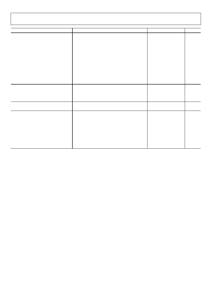
PIN CONFIGURATION AND FUNCTION DESCRIPTIONS
06
059
-
00
2
PIN 1
INDICATOR
1
COMM
2
VPOS
3
VPOS
4
VPOS
11 YPLS
12 YMNS
10 ZPLS
9 ZMNS
5
W
P
L
S
6
W
M
N
S
7
C
O
M
M
8
G
A
D
J
1
5
E
N
B
L
1
6
V
M
I
D
1
4
X
M
N
S
1
3
X
P
L
S
ADL5391
Figure 2. Pin Configuration
Table 3. Pin Function Descriptions
Pin No.
Mnemonic
Description
1, 7
COMM
Device Common. Connect via lowest possible impedance to external circuit common.
2 to 4
V
POS
Positive Supply Voltage. 4.5 V to 5.5 V.
5, 6
WPLS, WMNS
Differential Outputs.
8
GADJ
Denominator Scaling Input.
9, 10
ZMNS, ZPLS
Differential Intercept Inputs. Must be ac-coupled. Differential impedance 50 nominal.
11, 12
YPLS, YMNS
Differential X-Multiplicand Inputs.
13, 14
XPLS, XMNS
Differential Y-Multiplicand Inputs.
15
ENBL
Chip Enable. High to enable.
16
VMID
V
POS
/2 Reference Output. Connect decoupling capacitor to circuit common.

ADL5391
Rev. 0 | Page 7 of 16
TYPICAL PERFORMANCE CHARACTERISTICS
GADJ = open.
3.0
≠3.0
≠2.5
≠2.0
≠1.5
≠1.0
≠0.5
0
0.5
1.0
1.5
2.0
2.5
≠2.5 ≠2.0 ≠1.5 ≠1.0 ≠0.5
0
0.5
1.0
1.5
2.0
2.5
W
DI
FF
(
V
DC
)
X
DIFF
(V
DC
)
Y = ≠2
Y = ≠1
Y = 0
Y = +1
Y = +2
0
605
9-
0
07
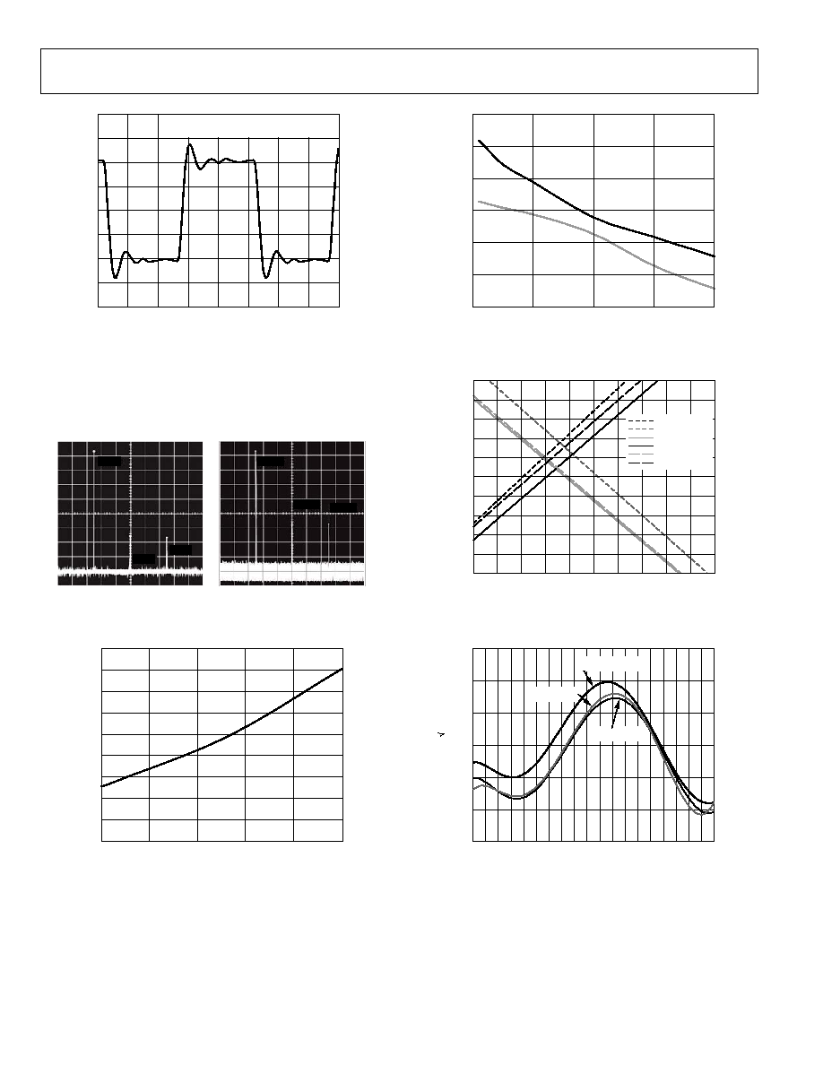
Figure 3. Full Range DC Cross Plots
0.20
≠0.20
≠0.15
≠0.10
≠0.05
0
0.05
0.10
0.15
≠0.20
≠0.15
≠0.10
≠0.05
0
0.05
0.10
0.15
0.20
W
DI
FF
(
V
DC
)
X
DIFF
(V
DC
)
Y = ≠2
Y = ≠1
Y = 0
Y = +1
Y = +2
0
605
9-
0
08
Figure 4. Magnified DC Cross Plots
2.5
2.0
1.5
1.0
0.5
0
≠1.0
2.0
1.5
1.0
0.5
0
≠0.5
GA
IN
(
V
/V
)
GADJ (V
DC
)
0
605
9-
0
09
Figure 5. Gain vs. GADJ (X = Y = 1)
14
≠14
200
≠200
≠150
≠100
≠50
≠0
50
100
150
≠12
≠10
≠8
≠6
≠4
≠2
0
2
4
6
8
10
12
200
0
191
0
181
0
172
0
162
0
153
0
143
0
134
0
124
0
115
0
105
0
955
860
765
670
575
480
385
290
195
100
5
GA
IN
(
d
B
)
P
HAS
E
(
D
eg
r
ees)
FREQUENCY (MHz)
06
05
9-
010
Figure 6. Gain and Phase vs. Frequency of X Swept and Y = 1 V, Z = 0 V,
P
IN
= 0 dBm
4
≠4
≠3
≠2
≠1
0
1
3
2
200
≠200
≠150
≠100
≠50
≠0
50
100
150
120
0
130
0
110
0
990
880
700
660
550
440
330
220
110
1
GA
IN
(
d
B
)
P
HAS
E
(
D
eg
r
ees)
FREQUENCY (MHz)
06
05
9-
011
Figure 7. Gain and Phase vs. Frequency of Z Inputs, X = 0 V, Y = 0 V,
P
IN
= 0 dBm
2.0
≠2.0
≠1.5
≠1.0
≠0.5
0
0.5
1.0
1.5
24.5
33.5
32.5
31.5
30.5
29.5
28.5
27.5
26.5
25.5
W
OU
T
P
U
T
(V
)
TIME (ns)
X ± INPUT = 1.0V p-p, @ 200MHz
Y ± INPUT = 1.0V DC DIFFERENTIAL
06
05
9-
0
13
Figure 8. Large Signal Pulse Response
ADL5391
Rev. 0 | Page 8 of 16
0.20
≠0.20
≠0.15
≠0.10
≠0.05
0
0.05
0.10
0.15
24.5
32.5
31.5
30.5
29.5
28.5
27.5
26.5
25.5
W
OU
T
P
U
T
(V
)
TIME (ns)
X ± INPUT = ±100mV p-p, @ 200MHz
Y ± INPUT = 1.0V DC DIFFERENTIAL
06
05
9-
0
14
Figure 9. Small Signal Pulse Response
0605
9-
094
200MHz
400MHz
600MHz
10MHz
30MHz
20MHz
1
0
d
B
m
/D
IV
1
0
d
B
m
/D
IV
Figure 10. Harmonic Distortion at 10 MHz and 200 MHz;
0 dBm Input to X (Y) Channels
28
26
24
22
20
18
16
14
12
10
≠40
≠15
10
35
60
8
AV
E
RAG
E
V
O
F
F
SET
(
5
V
DC
)
TEMPERATURE (∞C)
06
05
9-
0
15
Figure 11. X ( Y) Offset Drift vs. Temperature
30
0
5
10
15
20
25
0
2
Y = 1
Y = 0.5
1500
1000
500
OI
P
3
(
d
B
m
)
FREQUENCY (MHz)
000
06
05
9-
0
16
Figure 12. OIP3 vs. Frequency
Pin 0 dBm, Y = 1 V dc, 0.5 V dc
0.05
0.04
0.03
0.02
0.01
0
≠0.01
≠0.02
≠0.03
≠0.04
≠0.05
≠0.05
0.05
0.04
0.03
0.02
0.01
0
≠0.01
≠0.02
≠0.03
≠0.04
W
DI
FF
(
V
DC
)
Y
DIFF
(V
DC
)
+85∞C, X = +1
+85∞C, X = ≠1
≠40∞C, X = ≠1
≠40∞C, X = +1
+25∞C, X = ≠1
+25∞C, X = +1
06
05
9-
02
1
Figure 13. Z (W) Offset Over Temperature
45
15
20
25
30
35
40
2000
200
400
600
800
1000 1200 1400 1600 1800
SN
D
(
n
V/
H
z
)
FREQUENCY (MHz)
X = 0V, Y = 1V
X = Y = 1V
X = Y = 0V
06
05
9-
0
19
Figure 14. Noise vs. Frequency
ADL5391
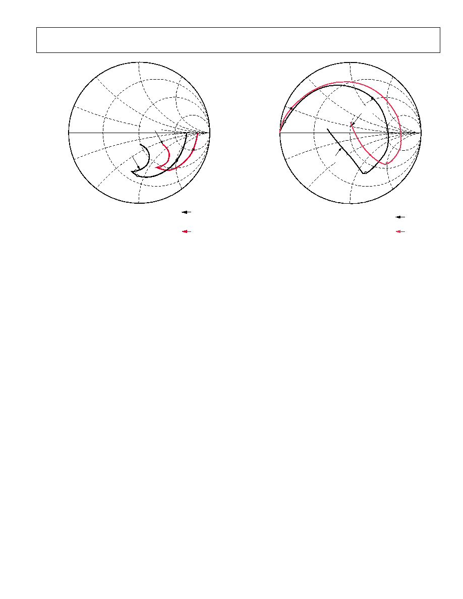
Rev. 0 | Page 9 of 16
1.00UFS
3001.000
S11 DIFF
1.000
201.000
0.654 U
≠36.340 DEG
1001.000
0.594 U
≠92.533 DEG
1901.000
0.531 U
≠94.448 DEG
201.000
0.800 U
≠17.218 DEG
2001.000
0.564 U
≠58.167 DEG
060
59
-
0
17
S11 SE
Figure 15. Input S11
1.00UFS
3001.000
1.000
201.000
0.947 U
+170.736 DEG
1001.000
0.569 U
+58.257 DEG
1901.000
0.597 U
≠69.673 DEG
201.000
0.905 U
+157.308 DEG
2001.000
0.663 U
≠39.468 DEG
06
05
9-
0
18
S22 DIFF
S22 SE
Figure 16. Output S22

ADL5391
Rev. 0 | Page 10 of 16
GENERAL DESCRIPTION
BASIC THEORY
The multiplication of two analog variables is a fundamental
signal processing function that has been around for decades.
By convention, the desired transfer function is given by
W = XY/U + Z
(1)
where:
X and Y are the multiplicands.
U is the multiplier scaling factor.
is the multiplier gain.
W is the product output.
Z is a summing input.
All the variables and the scaling factor have the dimension of volts.
In the past, analog multipliers, such as the
AD835
, were
implemented almost exclusively with a Gilbert Cell topology
or a close derivative. The inherently asymmetric signal paths
for X and Y inevitably create amplitude and delay imbalances
between X and Y. In the ADL5391, the novel multiplier core
provides absolute symmetry between X and Y, minimizing
scaling and phasing differences inherent in the Gilbert Cell.
The simplified block diagram of the ADL5391 shows a main
multiplier cell that receives inputs X and Y and a second
multiplier cell in the feedback path around an integrating
buffer. The inputs to this feedback multiplier are the difference
of the output signal and the summing input, W - Z, and the
internal scaling reference, U. At dc, the integrating buffer
ensures that the output of both multipliers is exactly 0, therefore
(W - Z)xU = XY, or W = XY/U + Z (2)
By using a feedback multiplier that is identical to the main
multiplier, the scaling is traced back solely to U, which is
an accurate reference generated on-chip. As is apparent in
Equation 2, noise, drift, or distortion that is common to both
multipliers is rejected to first-order because the feedback
multiplier essentially compensates the impairments generated
in the main multiplier.
The scaling factor, U, is fixed by design to 1.12 V. However, the
multiplier gain, , can be adjusted by driving the GADJ pin with
a voltage ranging from 0 V to 2 V. If left floating, then = 1 or
0 dB, and the overall scaling is simply U = 1 V. For VGADJ = 0 V,
the gain is lowered by approximately 4 dB; for VGADJ = 2 V,
the gain is raised by approximately 6 dB. Figure 5 shows the
relationship between (V/V) and VGADJ.
The small-signal bandwidth from the inputs X, Y, and Z to
the output W is a single-pole response. The pole is inversely
proportional to . For = 1 (GADJ floating), the bandwidth is
about 2 GHz; for > 1, the bandwidth is reduced; and for < 1,
the bandwidth is increased.
All input ports, X, Y, and Z, are differential and internally
biased to midsupply, V
POS
/2. The differential input impedance is
500 up to 100 MHz, rolling off to 50 at 2 GHz. All inputs
can be driven in single-ended fashion and can be ac-coupled. In
dc-coupled operation, the inputs can be biased to a common
mode that is lower than V
POS
/2. The bias current flowing out of
the input pins to accommodate the lower common mode is
subtracted from the 50 mA total available from the internal
reference V
POS
/2 at the VREF pin. Each input pin presents an
equivalent 250 dc resistance to V
POS
/2. If all six input pins sit
1 V below V
POS
/2, a total of 6 ◊ 1 V/250 = 24 mA must flow
internally from VREF to the input pins.
Calibration
The dc offset of the ADL5391 is approximately 20 mV but
changes over temperature and has variation from part to part
(see Figure 4). It is generally not of concern unless the ADL5391
is operated down to dc (close to the point X = 0 V or Y = 0 V),
where 0 V is expected on the output (W = 0 V). For example,
when the ADL5391 is used as a VGA and a large amount of
attenuation is needed, the maximum attenuation is determined
by the input dc offset.
Applying the proper voltage on the Z input removes the W
offset. Calibration can be accomplished by making the appropriate
cross plots and adjusting the Z input to remove the offset.
Additionally, gain scaling can be adjusted by applying a dc
voltage to the GADJ pin, as shown in Figure 5.
BASIC CONNECTIONS
Multiplier Connections
The best ADL5391 performance is achieved when the X, Y, and
Z inputs and W output are driven differentially; however, they
can be driven single-ended. Single-ended-to-differential
transformations (or differential-to-single-ended transformations)
can be done using a balun or active components, such as the
AD8313
, the
AD8132
(both with operation down to dc), or the
AD8352
(for higher drive capability). If using the ADL5391
single-ended without ac coupling capacitors, the reference
voltage of 2.5 V needs to be taken into account. Voltages above
2.5 V are positive voltages and voltages below 2.5 V are negative
voltages. Care needs to be taken not to load the ADL5391 too
heavily, the maximum reference current available is 50 mA.
ADL5391
Rev. 0 | Page 11 of 16
Matching the Input/Output
The input and output impedance's of the ADL5391 change over
frequency, making it difficult to match over a broad frequency
range (see Figure 15 and Figure 16). The evaluation board is
matched for lower frequency operation, and the impedance
change at higher frequencies causes the change in gain seen in
Figure 6. If desired, the user of the ADL5391 can design a
matching network to fit their application.
Wideband Voltage-Controlled Amplifier/Amplitude
Modulator
Most of the data for the ADL5391 was collected by using it as a
fast reacting analog VGA. Either X or Y inputs can be used for
the RF input (and the other as the very fast analog control),
because either input can be used from dc to 2 GHz. There is a
linear relationship between the analog control and the output of
the multiplier in the VGA mode. Figure 6 and Figure 7 show the
dynamic range available in VGA mode (without optimizing the
dc offsets).
The speed of the ADL5391 in VGA mode allows it to be used as
an amplitude modulator. Either or both inputs can have
modulation or CW applied. AM modulation is achieved by
feeding CW into X (or Y) and adding AM modulation to the Y
(or X) input.
Squaring and Frequency Doubling
Amplitude domain squaring of an input signal, E, is achieved
simply by connecting the X and Y inputs in parallel to produce
an output of E
2
. The input can be single-ended, differential, or
through a balun (frequency range and dynamic range can be
limited if used single ended).
When the input is a sine wave Esin(t), a signal squarer behaves
as a frequency doubler, because
[
]
(
)
(
t
E
t
E
2
-
=
2
cos
1
2
)
sin(
2
)
(3)
Ideally, when used for squaring and frequency doubling, there is
no component of the original signals on the output. Because of
internal offsets, this is not the case. If Equation 3 were rewritten
to include theses offsets, it could separate into three output
terms (Equation 4).
[
]
[
]
[
]
+
+
+
=
+
◊
+
2
)
sin(
2
)
cos(2
2
)
sin(
)
sin(
2
2
2
E
OFST
OFST
t
E
t
E
OFST
t
E
OFST
t
E
(4)
where:
The dc component is OFST
2
+ E
2
/2.
The input signal bleedthrough is 2Esin(t)OFST.
The input squared is E
2
/2[cos(2t)].
The dc component of the output is related to the square of both
the offset (OFST) and the signal input amplitude (E). The offset
can be found in Figure 4 and is approximately 20 mV. The
second harmonic output grows with the square of the input
amplitude, and the signal bleedthrough grows proportionally
with the input signal. For smaller signal amplitudes, the signal
bleedthrough can be higher than the second harmonic
component. As the input amplitude increases, the second
harmonic component grows much faster than the signal
bleedthrough and becomes the dominant signal at the output.
If the X and Y inputs are driven too hard, third harmonic
components will also increase.
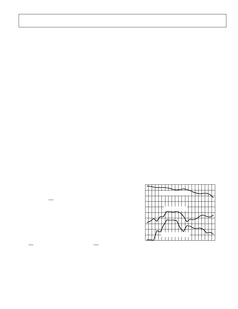
For best performance creating harmonics, the ADL5391 should
be driven differentially. Figure 17 shows the performance of the
ADL5391 when used as a harmonic generator (the evaluation
board was used with R9 and R10 removed and R2 = 56.2 ). If
dc operation is necessary, the ADL5391 can be driven single
ended (without the dc blocks). The flatness of the response over
a broad frequency range depends on the input/output match.
The fundamental bleed through not only depends on the
amount of power put into the device but also depends on
matching the unused differential input/output to the same
impedance as the used input/output. Figure 18 shows the
performance of the ADL5391 when driven single ended
(without ac coupling capacitors), and Figure 19 shows the
schematic of the setup. A resistive input/output match were
used to match the input from dc to 1 GHz and the output from
dc to 2 GHz. Reactive matching can be used for more narrow
frequency ranges. When matching the input/output of the
ADL5391, care needs to be taken not to load the ADL5391 too
heavily; the maximum reference current available is 50 mA.
≠15
≠65
≠60
≠55
≠50
≠45
≠40
≠35
≠30
≠25
≠20
10
100
200
300
400
500
600
700
800
900 1000
GA
IN
(
d
B
m
)
FREQUENCY (MHz)
SECOND HARMONIC GAIN
BLEEDTHRU GAIN
THIRD HARMONIC GAIN
06
05
9-
0
26
Figure 17. ADL5391 Used as a Harmonic Generator

ADL5391
Rev. 0 | Page 12 of 16
0
≠65
≠60
≠55
≠50
≠45
≠40
≠35
≠30
≠25
≠20
≠15
≠10
≠5
10
100
200
300
400
500
600
700
800
900 1000
GA
IN
(
d
B
m
)
FREQUENCY (MHz)
BLEEDTHRU GAIN
SECOND HARMONIC GAIN
THIRD HARMONIC GAIN
06
05
9-
0
27
Figure 18. Single-Ended (DC) ADL5391 Used as a Harmonic Generator
21
74
21
74
XIN
YIN
150
62
5dB PAD
5dB PAD
10dB PAD
53
53
200
XM
XP
YM
YP
WP
WM
06
05
9
-
02
8
Figure 19. Setup for Single-Ended Data
Use as a Detector
The ADL5391 can be used as a square law detector. When
amplitude squaring is performed, there are components of the
multiplier output that correlate to the signal bleedthrough and
second harmonic, as seen in Equation 4. However, as noted in
the Squaring and Frequency Doubling section, there is also a dc
component that is directly related to the offset and the squared
input magnitude. If a signal is split and feed into the X and Y
inputs and a low-pass filter were place on the output, the resulting
dc signal would be directly related to the square of the input
magnitude. The intercept of the response will shift slightly from
part to part (and over temperature) with the offset, but this can
be removed through calibration. Figure 20 shows the response
of the ADL5391 as a square law detector, Figure 21 shows the
error vs. the input power, and Figure 22 shows the
configuration used.
0.7
0.6
0.5
0.4
0.3
0.2
0.1
0
0
0
0.7
0.6
0.5
0.4
0.3
0.2
0.1
V
OU
T
(V
)
V
IN
(V rms)
2
06
05
9-
09
1
.8
Figure 20. ADL5391 Used as Square Law Detector DC Output vs. Square of Input
1.6
≠0.2
0
0.2
0.4
0.6
0.8
1.0
1.2
1.4
≠30
10
5
0
≠5
≠10
≠15
≠20
≠25
E
R
RO
R (
d
B)
PIN X (dBm)
06
05
9-
09
2
Figure 21. ADL5391Used as a Square Law Detector Error vs. Power Input
0
60
59
-
0
93
T1
45nF
40µH
40µH
74µH
74µH
J2
WM
J1
WP
XM
XP
YM
YP
11
12
13
14
WP
WM
6
5
R2
56.2
TC1-1-13M
T3
C7
0.1µF
C18
0.1µF
J6
YP
R1
56.2
TC1-1-13M
T2
C4
0.1µF
C20
0.1µF
J8
XP
R4
100
R12
OPEN
40nF
R6
24.9
R5
24.9
Figure 22. Schematic for ADL5391 Used as Square Law Detector
ADL5391
Rev. 0 | Page 13 of 16
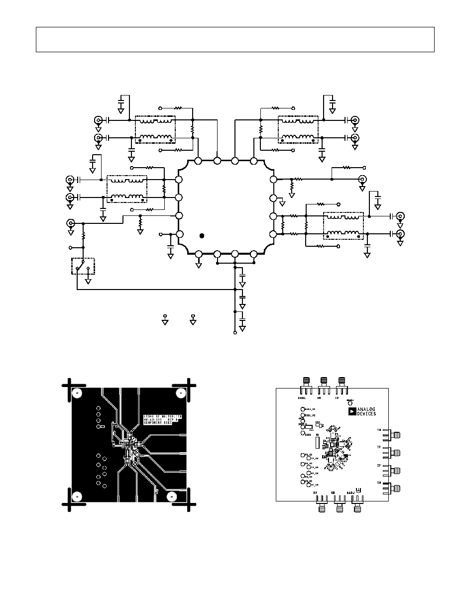
EVALUATION BOARD
R1
56.2
COMM
VPOS
VPOS
VPOS
WMNS
GADJ
ZPLS
ZMNS
WPLS
COMM
YMNS
YPLS
XMNS
XPLS
ENBL
VMID
T1
VPOS
TP13
TP
COMM
TP12
C10
100pF
C12
0.1µF
2
3
1
4
5
6
7
8
9
11
12
13
14
15
16
10
C11
4.7µF
TC1-1-13M
R5
24.9
R6
24.9
R4
100
R12
OPEN
WP_DC
TP1
R7
OPEN
WP
J1
WM
J2
C2
0.1µF
C5
OPEN
C13
OPEN
C14
0.1µF
R11
OPEN
R19
0
GADJ
J3
TC1-1-13M
R3
ZM_DC
TP4
ZP_DC
TP5
R15
0
R14
0
ZM
J4
ZP
J5
C9
OPEN
C8
0.1µF
C17
0.1µF
T4
C15
OPEN
OPEN
TP
COMM
TP14
R2
OPEN
R10
0
R9
0
T3
C16
OPEN
TC1-1-13M
YM_DC
TP7
YP_DC
TP6
YM
J7
YP
J6
C7
0.1µF
C6
OPEN
C18
0.1µF
R16
OPEN
R17
OPEN
T2
C19
OPEN
TC1-1-13M
XM_DC
TP9
XP_DC
TP8
XM
J9
XP
J8
C4
0.1µF
C1
OPEN
C20
0.1µF
WM_DC
TP2
R13
OPEN
1
3
SW1
C3
0.1µF
VMID
TP11
2
R8
OPEN
ENBL_DC
TP10
ENBL
J10
R20
0
GADJ_DC
TP3
R18
0
06
05
9-
0
25
ADL5391
Figure 23. ADL5391-EVALZ Evaluation Board Schematic
06
05
9-
03
0
Figure 24. Component Side Metal of Evaluation Board
0
60
59
-
03
1
Figure 25. Component Side Silkscreen of Evaluation Board

ADL5391
Rev. 0 | Page 14 of 16
Table 4. Evaluation Board Configuration Options
Component Function
Part
Number
Default
Value
J1, J5, J6, J8
SMA connectors for single-ended, high frequency operation. If J5
and J6 are used, R9, R10, R14, and R15 should be removed. R2 and
R3 should also be populated to match the inputs. If used in broadband
operation, C4, C7, C8, and C2 need to be replaced with 0 resistors.
WP, ZP, YP, XP
J2, J4, J7, J9
SMA connectors for broadband differential operation. If these are
used, baluns should be removed and jumped over using 0
resistors, and C14, C15, C18, and C20 should be removed.
WM, ZM, YM, XM
J3
SMA connector for connection to GADJ.
GADJ
T1, T2, T3, T4
Single-ended-to-differential transformation for high frequency ac
operation. If dc operation is necessary, the baluns can be removed
and jumped over using 0 resistors.
TC1-1-13M+
Mini-Circuits
T3 and T4 are populated,
but the Y and Z inputs
are set up for dc operation.
C2, C4, C7, C8, C14,
C17, C18, C20
DC block capacitors.
0.1 F, 0402 capacitors
C1, C5, C6, C9, C13,
C15, C16, C19
Not installed, dc block capacitors.
Open, 0402 capacitors
R9, R10, R14, R15, R18
Snubbing resistors.
0 , 0402 resistors
R19, R20
Snubbing resistors.
0 , 0603 resistors
R7, R13, R16, R17
Snubbing resistors.
Open, 0402 resistors
C10
Filter capacitor.
100 pF, 0402 capacitor
C12
Filter capacitor.
0.1 F, 0402 capacitor
C3
Filter capacitor.
0.1 F, 0603 capacitor
C11
Filter capacitor.
4.7 F, 3216 capacitor
R1
Matching resistor.
56.2 , 0603 resistor
R2, R3, R12
Matching resistors. Input impedance to X, Y, and Z inputs are the
same. For the same frequency, R1, R2, and R3 should be the same.
Open, 0603 resistors
R5, R6
Matching resistor.s
24.9 , 0402 resistors
R4
Matching resistor.
100 , 0603 resistor
R8, R11
Can be used for voltage divider or filtering.
Open, 0603 resistors
SW1
Enable switch: enable = 5 V, disable = 0 V.
SW1 installed
TP1, TP2, TP4, TP5,
TP6, TP7, TP8, TP9
Green test loop.
WP_DC, WM_DC,
ZM_DC, ZP_DC, YP_DC,
YM_DC, XP_DC, XM_DC
TP13
Red test loop.
V
POS
TP12, TP14
Black test loops.
COMM
TP3, TP10, TP11
Yellow test loops.
GADJ_DC,
ENBL_DC,
VMID
DUT ADL5391.
ADL5391ACPZ

ADL5391
Rev. 0 | Page 15 of 16
OUTLINE DIMENSIONS
1
0.50
BSC
0.60 MAX
PIN 1
INDICATOR
1.50 REF
0.50
0.40
0.30
0.25 MIN
0.45
2.75
BSC SQ
TOP
VIEW
12∞ MAX
0.80 MAX
0.65 TYP
SEATING
PLANE
PIN 1
INDICATOR
0.90
0.85
0.80
0.30
0.23
0.18
0.05 MAX
0.02 NOM
0.20 REF
3.00
BSC SQ
*1.65
1.50 SQ
1.35
16
5
13
8
9
12
4
EXPOSED
PAD
(BOTTOM VIEW)
*COMPLIANT TO JEDEC STANDARDS MO-220-VEED-2
EXCEPT FOR EXPOSED PAD DIMENSION.
Figure 26. 16-Lead Lead Frame Chip Scale Package [LFCSP_VQ]
3 mm ◊ 3 mm Body, Very Thin Quad
(CP-16-3)
Dimensions shown in millimeters
ORDERING GUIDE
Model Temperature
Range
Package
Description
Package Option
Ordering Quantity
ADL5391ACPZ-R2
1
-40∞C to +85∞C
16-Lead LFCSP_VQ
CP-16-3
250
ADL5391ACPZ-R7
1
-40∞C to +85∞C
16-Lead LFCSP_VQ
CP-16-3
1,500
ADL5391ACPZ-WP
1
-40∞C to +85∞C
16-Lead LFCSP_VQ
CP-16-3
50
ADL5391-EVALZ
1
Evaluation
Board
1
1
Z = Pb-free part.

ADL5391
Rev. 0 | Page 16 of 16
T
NOTES
©2006 Analog Devices, Inc. All rights reserved. Trademarks and
registered trademarks are the property of their respective owners.
D06059-0-7/06(0)
TTT