
ACS704ELC-005
115 Northeast Cutoff, Box 15036
Worcester, Massachusetts 01615-0036 (508) 853-5000
www.allegromicro.com
ACS704ELC005-DS, Rev. 5
AB SO LUTE MAX I MUM RAT INGS
Supply Voltage, V
CC
.......................................... 16 V
Reverse Supply Voltage, V
RCC
........................≠16 V
Output Voltage, V
OUT
........................................16 V
Reverse Output Voltage, V
ROUT
......................≠0.1 V
Output Current Source, I
OUT(Source)
................. 3 mA
Output Current Sink, I
OUT(Sink)
.......................10 mA
Operating Temperature,
Maximum
Junction,
T
J(max)
....................... 165∞C
Storage Temperature, T
S
......................≠65 to 170∞C
Features and Benefits
∑ Small footprint, low-profile SOIC8 package
∑ 1.5
m internal conductor resistance
∑ Excellent replacement for sense resistors
∑ 800
V
RMS
minimum isolation voltage beween pins 1-4 and 5-8
∑ 4.5 to 5.5 V, single supply operation
∑ 50 kHz bandwidth
∑ 133 mV/A output sensitivity and 15 A dynamic range
∑ Output voltage proportional to ac and dc currents
∑ Factory-trimmed for accuracy
∑ Extremely stable output offset voltage
∑ Near-zero magnetic hysteresis
∑ Ratiometric output from supply voltage
The Allegro ACS704 family of current sensors provides economical and
precise solutions for current sensing in industrial, automotive, commercial, and
communications systems. The device package allows for easy implementation
by the customer. Typical applications include motor control, load detection and
management, switched-mode power supplies, and overcurrent fault protection.
The device consists of a precision, low-offset linear Hall sensor circuit with
a copper conduction path located near the surface of the die. Applied current
flowing through this copper conduction path generates a magnetic field which is
sensed by the integrated Hall IC and converted into a proportional voltage. Device
accuracy is optimized through the close proximity of the magnetic signal to the
Hall transducer. A precise, proportional voltage is provided by the low-offset,
chopper-stabilized BiCMOS Hall IC, which is programmed for accuracy at the
factory.
The output of the device has a positive slope (>V
CC
/ 2) when an increasing current
flows through the primary copper conduction path (from pins 1 and 2, to pins 3
and 4), which is the path used for current sensing. The internal resistance of this
conductive path is typically 1.5 m, providing low power loss. The thickness
of the copper conductor allows survival of the device at up to 5◊ overcurrent
conditions. The terminals of the conductive path are electrically isolated from the
sensor leads (pins 5 through 8). This allows the ACS704 family of sensors to be
used in applications requiring electrical isolation without the use of opto-isolators
or other costly isolation techniques.
The ACS704 is provided in a small, surface mount SOIC8 package. The leadframe
is plated with 100% matte tin, which is compatible with standard lead (Pb) free
printed circuit board assembly processes. Internally, the flip-chip uses high-
temperature Pb-based solder balls, currently exempt from RoHS and WEEE. The
device is fully calibrated prior to shipment from the factory.
Package LC
Use the following complete part number when ordering:
Part Number
Package
ACS704ELC-005
SOIC8 surface mount
TÐV America
Certificate Number:
U8V 04 12 54214 005
5
4
3
2
1
6
7
8
*
100 total pulses, 250 ms duration each, applied at a rate of
1 pulse every 100 seconds.
Nominal Operating Temperature, T
A
Range
E............................................ ≠40 to 85∫C
Overcurrent Transient Tolerance*, I
P
................ 60 A
Fully Integrated, Hall Effect-Based Linear Current Sensor
with Voltage Isolation and a Low-Resistance Current Conductor
Pin 1: IP+
Pin 2: IP+
Pin 3: IP≠
Pin 4: IP≠
Pin 5: GND
Pin 6: VOUT
Pin 7: VOUT
Pin 8: VCC

2
115 Northeast Cutoff, Box 15036
Worcester, Massachusetts 01615-0036 (508) 853-5000
www.allegromicro.com
ACS704ELC005-DS, Rev. 5
ACS704ELC-005
Amp
Out
VCC
+5 V
Pin 8
Pin 7
VOUT
Pin 6
VOUT
GND
Pin 5
Filter
Dynamic Of
fset
Cancellation
IP+ IP+
0.1 F
Pin 1 Pin 2
IP≠
IP≠
Pin 3 Pin 4
Gain
Temperature
Coefficient
Offset
Voltage
Regulator
Trim Control
To all subcircuits
Functional Block Diagram

3
115 Northeast Cutoff, Box 15036
Worcester, Massachusetts 01615-0036 (508) 853-5000
www.allegromicro.com
ACS704ELC005-DS, Rev. 5
ACS704ELC-005
PERFORMANCE CHARACTERISTICS
, T
A
= ≠40∞C to 85∞C, V
CC
= 5 V unless otherwise specified
Propagation Time
t
PROP
I
P
=±5 A, T
A
= 25∞C
≠
4
≠
s
Response Time
t
RESPONSE
I
P
=±5 A, T
A
= 25∞C
≠
8
≠
s
Rise Time
t
r
I
P
=±5 A, T
A
= 25∞C
≠
9
≠
s
Frequency Bandwidth
f
≠3 dB, T
A
= 25∞C; I
P
is 10 A peak-to-
peak; no external filter
≠
50
≠
kHz
Sensitivity
Sens
Over full range of I
P
,
I
P
applied for 5 ms; T
A
= 25∞C
≠
133
≠
mV/A
Over full range of I
P
,
I
P
applied for 5 ms; T
A
= ≠40 to 85∞C
124
≠
142
mV/A
Noise
V
NOISE
Peak-to-peak, T
A
= 25∞C,
no external filter
≠
90
≠
mV
Root Mean Square, T
A
= 25∞C,
no external filter
≠
16
≠
mV
Linearity
E
LIN
Over full range of I
P
,
I
P
applied for 5 ms; T
A
= ≠40 to 85∞C
≠
±1
±4.7
%
Symmetry
E
SYM
Over full range of I
P
,
I
P
applied for 5 ms; T
A
= ≠40 to 85∞C
98
100
104.5
%
Zero Current Output Voltage
V
OUT(Q)
I
P
= 0 A, T
A
= 25∞C
≠
V
CC
/ 2
≠
V
Electrical Offset Voltage
V
OE
I
P
= 0 A, T
A
= 25∞C
≠15
≠
15
mV
I
P
= 0 A, T
A
= ≠40 to 85∞C
≠65
≠
65
mV
Magnetic Offset Error
I
ERROM
I
P
= 0 A, after excursion of 8.3 A;
T
A
= ≠40 to 85∞C
≠
±0.01
±0.05
A
Total Output Error
2
E
TOT
I
P
=±5 A
, I
P
applied for 5 ms;
T
A
= 25∞C
≠
±1.5
≠
%
I
P
= ±5 A
, I
P
applied for 5 ms;
T
A
= ≠40 to 85∞C
≠
≠
±12.5
%
1
Device may be operated at higher primary current, I
P
, and Ambient Temperature, T
A
, levels, provided that the Maximum Junction Temperature, T
J(max)
,
is not exceeded.
2
Percentage of I
P
, with I
P
= 5 A; Output filtered. Up to a 2.0% shift in E
TOT
may be observed at end-of-life for this device.
ELECTRICAL CHARACTERISTICS,
over operating ambient temperature range unless otherwise stated
Characteristic
Symbol
Test Conditions
Min.
Typ.
Max.
Units
Primary Sensed Current
1
I
P
≠5
≠
5
A
Supply Voltage
V
CC
4.5
5.0
5.5
V
Supply Current
I
CC
V
CC
= 5.0 V, output open
5
8
10
mA
Output Resistance
R
OUT
I
OUT
= 1.2 mA
≠
1
2
Output Capacitance Load
C
LOAD
VOUT to GND
≠
≠
10
nF
Output Resistive Load
R
LOAD
VOUT to GND
4.7
≠
≠
k
Primary Conductor Resistance
R
PRIMARY
T
A
= 25∞C
≠
1.5
≠
m
Isolation Voltage
V
ISO
Pins 1-4 and 5-8; 60 Hz, 1 minute
800
1200
≠
V

4
115 Northeast Cutoff, Box 15036
Worcester, Massachusetts 01615-0036 (508) 853-5000
www.allegromicro.com
ACS704ELC005-DS, Rev. 5
ACS704ELC-005
Typical Performance Characteristics
-50
-25
0
25
50
75
100
125
150
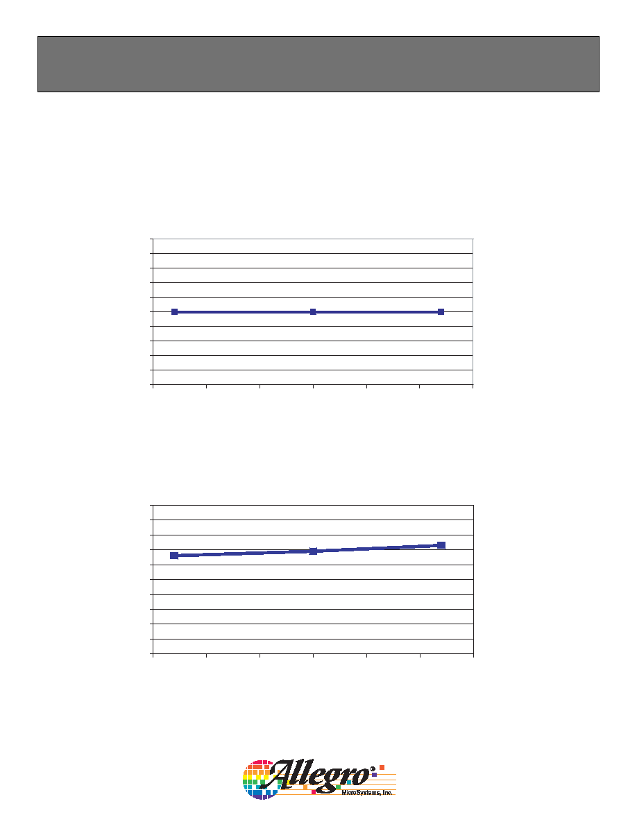
Supply Current versus Ambient Temperature
V
CC
= 5 V
T
A
(∞C)
I
CC
(mA
)
6.0
6.4
6.8
7.2
7.6
8.0
8.4
8.8
9.2
9.6
10.0
4.5
4.6
4.7
4.8
4.9
5
5.1
5.2
5.3
5.4
5.5
Supply Current versus Applied V
CC
V
CC
(V)
I
CC
(mA
)
8.44
8.46
8.48
8.50
8.52
8.54
8.56
8.58
8.60
8.62
8.64
8.66

5
115 Northeast Cutoff, Box 15036
Worcester, Massachusetts 01615-0036 (508) 853-5000
www.allegromicro.com
ACS704ELC005-DS, Rev. 5
ACS704ELC-005
1.0
1.3
1.6
1.9
2.2
2.5
2.8
3.1
3.4
3.7
4.0
-9
-8
-7
-6
-5
-4
-3
-2
-1
0
1
2
3
4
5
6
7
8
9
V
OUT
(V
)
-40
25
85
∞C
Output Voltage versus Primary Current
V
CC
= 5 V
I
P
(A)
110
115
120
125
130
135
140
145
150
-10 -9
-8
-7
-6
-5
-4
-3
-2
-1
0
1
2
3
4
5
6
7
8
9
10
Sens (mV/A)
-40
25
85
∞C
Sensitivity versus Primary Current
V
CC
= 5 V
I
P
(A)

6
115 Northeast Cutoff, Box 15036
Worcester, Massachusetts 01615-0036 (508) 853-5000
www.allegromicro.com
ACS704ELC005-DS, Rev. 5
ACS704ELC-005
-50
-25
0
25
50
75
100
125
150
V
OUT(Q)
(V
)
2.480
2.484
2.488
2.492
2.496
2.500
2.504
2.508
2.512
2.516
2.520
Zero Current Output Voltage vs. Ambient Temperature
T
A
(∞C)
I
P
= 0 A
-50
-25
0
25
50
75
100
125
150
Zero Current Output Currrent versus Ambient Temperature
(Data in above chart converted to amperes)
T
A
(∞C)
I
P
= 0 A
I
VOUT(Q)
(A)
-0.20
-0.16
-0.12
-0.08
-0.04
0
0.04
0.08
0.12
0.16
0.20
7
115 Northeast Cutoff, Box 15036
Worcester, Massachusetts 01615-0036 (508) 853-5000
www.allegromicro.com
ACS704ELC005-DS, Rev. 5
ACS704ELC-005
-50
-25
0
25
50
75
100
V
OM
(A
)
Magnetic Offset Error versus Ambient Temperature
V
CC
= 5 V; I
P
= 0 A, after excursion to 8.33 A
T
A
(∞C)
-1.0
-0.8
-0.6
-0.4
-0.2
0
0.2
0.4
0.6
0.8
1.0
0
0.1
0.2
0.3
0.4
0.5
0.6
0.7
0.8
0.9
1.0
E
LIN
(%)
-50
-25
0
25
50
75
100
Nonlinearity versus Ambient Temperature
V
CC
= 5 V
I
P
= 5 A
T
A
(∞C)
8
115 Northeast Cutoff, Box 15036
Worcester, Massachusetts 01615-0036 (508) 853-5000
www.allegromicro.com
ACS704ELC005-DS, Rev. 5
ACS704ELC-005
Measurements taken at TA = ≠40, 25, and 85 degrees C
-5
-4
-3
-2
-1
0
1
2
3
4
5
6
7
T
A
(∞C)
E
TOT
(
%
o
f5A
)
Mean + 3 Sigma
Mean ≠ 3 Sigma
Mean
-40
-20
0
20
40
60
80
Typical Percentage Error versus Ambient Temperature
-7.0
-6.0
-5.0
-4.0
-3.0
-2.0
-1.0
0
0
10
20
30
40
50
60
70
3 A
5 A
10 A
dB Change fr
o
m
5 kHz Response
AC Current Frequency (kHz)
Attenuation of ACS704 Output versus AC Sinusoidal Current Frequency

9
115 Northeast Cutoff, Box 15036
Worcester, Massachusetts 01615-0036 (508) 853-5000
www.allegromicro.com
ACS704ELC005-DS, Rev. 5
ACS704ELC-005
Typical Peak-to-Peak Noise of ACS704ELC-005 at T
A
=25∞C
Step Response of ACS704ELC-005 at T
A
=25∞C
ACS704 Output (mV)
5 A Excitation Signal

10
115 Northeast Cutoff, Box 15036
Worcester, Massachusetts 01615-0036 (508) 853-5000
www.allegromicro.com
ACS704ELC005-DS, Rev. 5
ACS704ELC-005
Break Frequency
of Filter on Output
(k Hz)
Nominal
Programmed
Sensitivity
(mV/A)
Unfiltered
Peak-to-Peak
Noise
(mV)
Filtered Peak-
to-Peak Noise
(mV)
Resolution
with Filtering
(A)
Measured Rise
Time for 5 A Step,
filtered
(s)
Unfiltered
133
90
90
0.67
8
40
47
0.35
12.5
10
25
0.20
35
7.0
22
0.17
46
3.9
12
0.10
90
ACS704ELC-005 Noise Filtering and Frequency Response Performance

11
115 Northeast Cutoff, Box 15036
Worcester, Massachusetts 01615-0036 (508) 853-5000
www.allegromicro.com
ACS704ELC005-DS, Rev. 5
ACS704ELC-005
Definitions of Accuracy Characteristics
Sensitivity (Sens). The change in sensor output in response to a 1 A change through the primary conductor. The sensitivity is the prod-
uct of the magnetic circuit sensitivity (G / A) and the linear IC amplifier gain (mV/G). The linear IC amplifier gain is programmed at the
factory to optimize the sensitivity (mV/A) for the full-scale current of the device.
Noise (V
NOISE
). The product of the linear IC amplifier gain (mV/G) and the noise floor for the Allegro Hall effect linear IC (1 G).
The noise floor is derived from the thermal and shot noise observed in Hall elements. Dividing the noise (mV) by the sensitivity
(mV/A) provides the smallest current that the device is able to resolve.
Linearity (E
LIN
): The degree to which the voltage output from the sensor varies in direct proportion to the primary current through its
full-scale amplitude. Nonlinearity in the output can be attributed to the saturation of the flux concentrator approaching the full-scale
current. The following equation is used to derive the linearity:
Definitions of Accuracy Characteristics
100 1≠
[{
[ {
Vout_full-scale amperes ≠ V
OUT(Q)
(
)
2 (Vout_half-scale amperes ≠ V
OUT(Q)
)
100
Vout_+full-scale amperes ≠ V
OUT(Q)
V
OUT(Q)
≠Vout_≠full-scale amperes
where V
out_full-scale amperes
= the output voltage (V) when the sensed current approximates full-scale ±I
P
.
Symmetry (E
SYM
). The degree to which the absolute voltage output from the sensor varies in proportion to either a positive or nega-
tive full-scale primary current. The following formula is used to derive symmetry:
Quiescent output voltage (V
OUT(Q)
). The output of the sensor when the primary current is zero. For a unipolar supply voltage, it
nominally remains at V
CC
/ 2. Thus, V
CC
= 5 V translates into V
OUT(Q)
= 2.5 V. Variation in V
OUT(Q)
can be attributed to the resolution
of the Allegro linear IC quiescent voltage trim and thermal drift.
Electrical offset voltage (V
OE
). The deviation of the device output from its ideal quiescent value of V
CC
/ 2 due to nonmagnetic causes.
To convert this voltage to amperes, divide by the device sensitivity, Sens.
Accuracy (E
TOT
). The accuracy represents the maximum deviation of the actual output from its ideal value. This is also known as the
total ouput error. The accuracy is illustrated graphically in the Output Voltage versus Current chart on the following page.
Accuracy is divided into four areas:
∑ 0 A at 25∞C. Accuracy of sensing zero current flow at 25∞C, without the effects of temperature.
∑ 0 A over temperature. Accuracy of sensing zero current flow including temperature effects.
∑ Full-scale current at 25∞C. Accuracy of sensing the full-scale current at 25∞C, without the effects of temperature.
∑ Full-scale current over temperature. Accuracy of sensing full-scale current flow including temperature effects.
Ratiometry. The ratiometric feature means that its 0 A output, V
OUT(Q)
, (nominally equal to V
CC
/2) and sensitivity, Sens, are propor-
tional to its supply voltage, V
CC
. The following formula is used to derive the ratiometric change in 0 A output voltage,
V
OUT(Q)RAT
(%):
The ratiometric change in sensitivity,
Sens
RAT
(%), is defined as:
100
V
OUT(Q)VCC
/ V
OUT(Q)5V
V
CC
/ 5 V
100
Sens
VCC
/ Sens
5V
V
CC
/ 5 V

12
115 Northeast Cutoff, Box 15036
Worcester, Massachusetts 01615-0036 (508) 853-5000
www.allegromicro.com
ACS704ELC005-DS, Rev. 5
ACS704ELC-005
Increasing V
OUT
(V)
+I
P
(A)
Accuracy
Accuracy
Accuracy
25∞C Only
Accuracy
25∞C Only
Accuracy
25∞C Only
Accuracy
0 A
v r
O e Temperature
Average
V
OUT
≠I
P
(A)
v r
O e Temperature
v r
O e Temperature
Decreasing V
OUT
(V)
≠5 A
5 A
Full Scale
Output voltage vs. current, illustrating sensor accuracy at 0 A and at full-scale current

13
115 Northeast Cutoff, Box 15036
Worcester, Massachusetts 01615-0036 (508) 853-5000
www.allegromicro.com
ACS704ELC005-DS, Rev. 5
ACS704ELC-005
Definitions of Dynamic Response Characteristics
Propagation delay (t
PROP
): The time required for the sensor output to reflect a change in the primary cur-
rent signal. Propagation delay is attributed to inductive loading within the linear IC package, as well as in the
inductive loop formed by the primary conductor geometry. Propagation delay can be considered as a fixed time
offset and may be compensated.
Response time (t
RESPONSE
): The time interval between a) when the primary current signal reaches 90% of its
final value, and b) when the sensor reaches 90% of its output corresponding to the applied current.
Rise time (t
r
): The time interval between a) when the sensor reaches 10% of its full scale value, and b) when
it reaches 90% of its full scale value. The rise time to a step response is used to derive the bandwidth of the
current sensor, in which (≠3 dB) = 0.35 / t
r
. Both t
r
and t
RESPONSE
are detrimentally affected by eddy current
losses observed in the conductive IC ground plane.
Primary Current
Transducer Output
90
0
I (%)
Propagation Time, t
PROP
t
Primary Current
Transducer Output
90
0
I (%)
Response Time, t
RESPONSE
t
Primary Current
Transducer Output
90
10
0
I (%)
Rise Time, t
r
t
14
115 Northeast Cutoff, Box 15036
Worcester, Massachusetts 01615-0036 (508) 853-5000
www.allegromicro.com
ACS704ELC005-DS, Rev. 5
ACS704ELC-005
Standards and Physical Specifications
Parameter
Specification
Flammability (package molding compound)
UL recognized to UL 94V-0
Fire and Electric Shock
UL60950-1:2003
EN60950-1:2001
CAN/CSA C22.2 No. 60950-1:2003
Device Branding Key (Two alternative styles are used)
ACS704T
ELC005
YYWWA
ACS
Allegro Current Sensor
704
Device family number
T
Indicator of 100% matte tin leadframe plating
E
Operating ambient temperature range code
LC
Package type designator
005
Primary sensed current
YY
Manufacturing date code: Calendar year (last two digits)
WW
Manufacturing date code: Calendar week
A
Manufacturing date code: Shift code
ACS704T
ELC005
L...L
YYWW
ACS
Allegro Current Sensor
704
Device family number
T
Indicator of 100% matte tin leadframe plating
E
Operating ambient temperature range code
LC
Package type designator
005
Primary sensed current
L...L
Manufacturing lot code
YY
Manufacturing date code: Calendar year (last two digits)
WW
Manufacturing date code: Calendar week

15
115 Northeast Cutoff, Box 15036
Worcester, Massachusetts 01615-0036 (508) 853-5000
www.allegromicro.com
ACS704ELC005-DS, Rev. 5
ACS704ELC-005
Amp
Regulator
Clock/Logic
Hall Element
Sa
mp
le
an
d
Ho
ld
Low-Pass
Filter
Chopper Stabilization Technique
Chopper Stabilization is an innovative circuit technique that is used to minimize the offset voltage of a Hall
element and an associated on-chip amplifier. Allegro patented a Chopper Stabilization technique that nearly
eliminates Hall IC output drift induced by temperature or package stress effects. This offset reduction technique
is based on a signal modulation-demodulation process. Modulation is used to separate the undesired dc offset
signal from the magnetically induced signal in the frequency domain. Then, using a low-pass filter, the modu-
lated dc offset is suppressed while the magnetically induced signal passes through the filter. As a result of this
chopper stabilization approach, the output voltage from the Hall IC is desensitized to the effects of temperature
and mechanical stress. This technique produces devices that have an extremely stable Electrical Offset Voltage,
are immune to thermal stress, and have precise recoverability after temperature cycling.
This technique is made possible through the use of a BiCMOS process that allows the use of low-offset and
low-noise amplifiers in combination with high-density logic integration and sample and hold circuits.
Concept of Chopper Stabilization Technique
16
115 Northeast Cutoff, Box 15036
Worcester, Massachusetts 01615-0036 (508) 853-5000
www.allegromicro.com
ACS704ELC005-DS, Rev. 5
ACS704ELC-005
Applications Information
In order to quantify transient common-mode voltage rejection for the ACS704, a device was soldered onto a printed
circuit board. A 0.1 F bypass capacitor and a 5 V dc power supply were connected between VCC and GND (pins 8 and
5) for this device. A 10 k load resistor and a 0.01 F capacitor were connected in parallel between the VOUT pin and
the GND pin of the device (pins 7 and 5).
A function generator was connected between the primary current conductor (pins 1 thru 4) and the GND pin of
the device (pin 5). This function generator was configured to generate a 10 V peak (20 V peak-to-peak) sine
wave between pins 1-4 and pin 5. Note that the sinusoidal stimulus was applied such that no electrical current
would flow through the copper conductor composed of pins 1-4 of this device.
The frequency of this sine wave was varied from 60 Hz to 5 MHz in discrete steps. At each frequency, the
statistics feature of an oscilloscope was used to measure the voltage variations (noise) on the ACS704 output
in mV (peak to peak). The noise was measured both before and after the application of the stimulus. Transient
common-mode voltage rejection as a function of frequency is shown in the following figure.
ACS704 Schematic Diagram of the Circuit used to Measure Transient Rejection
Transient Common-Mode Voltage Rejection in the ACS704
Output
Vcc
Ground
8
7
6
5
1
2
3
4
IP
V1
V
OUT
=0V
V
OUT
=20VPP
freq=variable
C3
C0
V0
GND
R0
C=0.01µF
C=0.1µF
VDC=5V
R=10k
(kHz)
0.06
1
10
100
300
600
800
1000 3000 5000
Frequency of 20 V Peak-to-Peak Stimulus
≠60
≠55
≠50
≠45
≠40
≠35
≠30
Tr
ansi
en
t
R
e
j
e
ct
i
o
n
(
d
B
)

17
115 Northeast Cutoff, Box 15036
Worcester, Massachusetts 01615-0036 (508) 853-5000
www.allegromicro.com
ACS704ELC005-DS, Rev. 5
ACS704ELC-005
The Effect of PCB Layout on ACS704 Electrical Performance
Eight different PC boards were fabricated to characterize the effect of PCB design on the operating junction temperature of the
Hall-effect IC inside of the ACS704. These PC boards are shown in the figure below.
2 oz. Cu on one side of board
2 oz. Cu on both sides of board
An ACS704 device was soldered onto each PC board before beginning the thermal testing. Thermal management tests
were conducted with the following test conditions:
Tests were conducted at ambient temperature, T
a
= 20
∞C. All tests were conducted in still air.
14 gauge wires were used to connect a power supply to a single PC board. These wires carry the 15 A dc primary current during
the tests.
A 15 A dc primary current was applied to a single PC board containing an ACS704 device. This current flowed from pins 1 and 2
to pins 3 and 4 of the ACS704 package.
A 1 mA current was forced from the GND pin to the VCC pin by a Fluke 179 True RMS Multimeter. This was the only power
applied to pins 5-8 of the ACS704 package during testing.
The voltage required to force the 1 mA current from the GND pin to the VCC pin was measured after applying the 15 A primary
current for approximately 25 minutes. A graph similar to the graph below was used to determine the junction temperature of the
ACS704.
Voltage vs. Temperature Curve used to Determine Die Junction Temperature

18
115 Northeast Cutoff, Box 15036
Worcester, Massachusetts 01615-0036 (508) 853-5000
www.allegromicro.com
ACS704ELC005-DS, Rev. 5
ACS704ELC-005
The results of the testing are shown in the following table.
Improved PC Board Designs
The eight PC boards in the figure above do not represent an ideal PC board for use with the ACS704. The ACS704 evaluation
boards, for sale at the Allegro Web site On-Line Store, represent a more optimal PC board design (see photo below). On the
evaluation boards, the current to be sensed flows through very wide traces that were fabricated using 2 layers of 2 oz. copper.
Thermal management tests were conducted on the Allegro evaluation boards and all tests were performed using the same test
conditions described in the bulleted list above. The results for these thermal tests are shown in the table below. When using
the Allegro evaluation boards we see that even at an applied current of 20 A the junction temperature of the ACS704 is only
~30 degrees above ambient temperature.
ACS704 Thermal Performance on the Allegro Eval PC Boards
Applied Current (A)
T
a
= 20
∞C, Still Air
Temp Rise Above Ambient
(
∞C)
15
22
20
31
Effect of PCB Layout on ACS704 Thermal Performance
Tested at 15A, T
A
= 20∞C, still air, 2 oz. copper traces
PC Boards
Sides with Traces
Trace Width (mm)
Trace Length (mm)
Temperature Rise
Above Ambient (∞C)
1
4
50
90
1.5
50
Overheated
4
10
48
1.5
10
110
2
4
50
53
1.5
50
106
4
10
38
1.5
10
54

19
115 Northeast Cutoff, Box 15036
Worcester, Massachusetts 01615-0036 (508) 853-5000
www.allegromicro.com
ACS704ELC005-DS, Rev. 5
ACS704ELC-005
Package LC, 8-pin SOIC
The products described herein are manufactured under one or more of the following U.S. patents: 5,045,920; 5,264,783; 5,442,283; 5,389,889;
5,581,179; 5,517,112; 5,619,137; 5,621,319; 5,650,719; 5,686,894; 5,694,038; 5,729,130; 5,917,320; and other patents pending.
Allegro MicroSystems, Inc. reserves the right to make, from time to time, such de par tures from the detail spec i fi ca tions as may be required to
permit improvements in the per for mance, reliability, or manufacturability of its products. Before placing an order, the user is cautioned to verify that
the information being relied upon is current.
Allegro products are not authorized for use as critical components in life-support devices or sys tems without express written approval.
The in for ma tion in clud ed herein is believed to be ac cu rate and reliable. How ev er, Allegro MicroSystems, Inc. assumes no re spon si bil i ty for its
use; nor for any in fringe ment of patents or other rights of third parties which may result from its use.
Copyright©2005, Allegro MicroSystems, Inc.
0.25
0.10
.010
.004
1.75
1.35
.069
.053
0.51
0.31
.020
.012
4.00
3.80
.157
.150
0.25
0.17
.010
.007
8∫
0∫
1.27
0.40
.050
.016
5.00
4.80
.197
.189
C
SEATING
PLANE
A
B
8X
0.25 [.010] M C
A
B
6.20
5.80
.244
.228
C
0.10 [.004]
8X
0.25 [.010] M B M
1.27 .050
0.25 .010
2
1
8
GAUGE PLANE
SEATING PLANE
Preliminary dimensions, for reference only
Dimensions in millimeters
U.S. Customary dimensions (in.) in brackets, for reference only
(reference JEDEC MS-012 AA)
Dimensions exclusive of mold flash, gate burrs, and dambar protrusions
Exact case and lead configuration at supplier discretion within limits shown
A Terminal #1 mark area
A