 | –≠–ª–µ–∫—Ç—Ä–æ–Ω–Ω—ã–π –∫–æ–º–ø–æ–Ω–µ–Ω—Ç: ATA01504 | –°–∫–∞—á–∞—Ç—å:  PDF PDF  ZIP ZIP |

08/2001
FEATURES
∑
Single +5 Volt Supply
∑
TO Package Compatible
∑
Automatic Gain Control
∑
-38 dBM Sensitivity
∑
0 dBm Overload
∑
175 MHz Bandwidth
APPLICATIONS
∑
SONET OC-3/SDH STM-1 (155 Mb/s) Receiver
∑
FDDI, Ethernet Fiber LAN
∑
Low Noise RF Amplifier
PRODUCT DESCRIPTION
Figure 1: Equivalent Circuit
ATA01504
AGC Transimpedance Amplifier
SONET OC-3
PRELIMINARY DATA SHEET-Rev 1
D1C
The ANADIGICS ATA01504 is a 5V low noise
transimpedance amplifier with AGC designed to be
used in OC-3/STM-1 fiber optic links. The device is
used in conjunction with a photodetector (PIN diode
or avalanche photodiode) to convert an optical signal
into an output voltage. The ATA01504 offers a
bandwidth of 175MHz, a dynamic range of 38dB and
an alternate pad layout as compared to the ATA01501.
It is manufactured in a GaAs MESFET process and
is available in bare die form.
V
OUT
C
AGC
GND
V
DD
I
IN
GND
or
neg.supply
- 45
VGA
70K
+
4.5 pF
+ 0.8
AGC
19K
US PATENT
5442321,5602510,5047728
Photodector cathode must be connected
to I
IN
for proper AGC operation
PRELIMINARY DATA SHEET - Rev 1
08/2001
2
ATA01504
Table 1: Pad Description
Figure 2: Bonding Pad Layout
ELECTRICAL CHARACTERISTICS
Table 2: Absolute Maximum Ratings
D
A
P
n
o
it
p
i
r
c
s
e
D
t
n
e
m
m
o
C
V
D
D
V
D
D
e
g
a
t
s
n
i
a
g
t
u
p
n
i
r
o
f
y
l
p
p
u
s
e
v
it
i
s
o
P
I
N
I
t
n
e
rr
u
C
t
u
p
n
I
A
I
T
n
o
it
a
r
e
p
o
r
e
p
o
r
p
r
o
f
e
d
o
h
t
a
c
r
o
t
c
e
t
e
d
t
c
e
n
n
o
C
V
T
U
O
e
g
a
tl
o
V
t
u
p
t
u
O
A
I
T
k
c
o
l
b
C
D
l
a
n
r
e
t
x
e
s
e
ri
u
q
e
R
C
C
G
A
r
o
ti
c
a
p
a
C
C
G
A
l
a
n
r
e
t
x
E
C
(
*
K
0
7
C
G
A
t
n
a
t
s
n
o
C
e
m
i
T
C
G
A
=
)
F
p
5
.
4
*
V
D
D
V
0
.
7
I
N
I
A
m
5
T
A
0
4
-
.
p
m
e
T
g
n
it
a
r
e
p
O
o
5
2
1
o
t
C
o
C
T
S
5
6
-
.
p
m
e
T
e
g
a
r
o
t
S
o
0
5
1
o
t
C
o
C
Stresses in excess of the absolute ratings may cause
permanent damage. Functional operation is not implied
under these conditions. Exposure to absolute ratings
for extended periods of time may adversely affect
reliability.

PRELIMINARY DATA SHEET - Rev 1
08/2001
3
ATA01504
Table 3: Electrical Specifications
(1)
(T
A
= 25
∞
C, V
DD
=+5.0V + 10%, C
DIODE
+ C
STRAY
= 0.5 pF, Det. cathode to I
IN
)
Notes:
1. f = 50MHz
2. Measured with I
in
below AGC Threshold. During AGC, input impedance will
decrease proportionally to I
in.
3. Defined as the I
in
where Transresistance has decreased by 50%.
4. See note on Indirect Measurement of Optical Overload.
5. See note on Measurement of Input Referred Noise Current.
6. C
AGC
= 220 pF
7. Parameter is guaranteed (not tested) by design and characterization data
@155 Mb/s, assuming dectector responsivity of 0.9.
R
E
T
E
M
A
R
A
P
N
I
M
P
Y
T
X
A
M
T
I
N
U
R
(
e
c
n
a
t
s
i
s
e
r
s
n
a
r
T
L
I,
=
C
D
)
A
n
0
0
5
<
7
1
K
R
(
e
c
n
a
t
s
i
s
e
r
s
n
a
r
T
L
)
0
5
=
)
1
(
5
.
5
8
0
1
K
B
d
3
-
h
t
d
i
w
d
n
a
B
0
5
1
5
7
1
z
H
M
e
c
n
a
t
s
i
s
e
R
t
u
p
n
I
)
2
(
0
0
5
e
c
n
a
t
s
i
s
e
R
t
u
p
t
u
O
0
3
0
5
0
6
t
n
e
rr
u
C
y
l
p
p
u
S
0
3
5
4
A
m
e
g
a
tl
o
V
t
e
s
ff
O
t
u
p
n
I
5
.
1
6
.
1
9
.
1
s
tl
o
V
e
g
a
tl
o
V
t
e
s
ff
O
t
u
p
t
u
O
8
.
1
s
tl
o
V
I(
d
l
o
h
s
e
r
h
T
C
G
A
N
I
)
)
3
(
5
1
0
3
d
a
o
lr
e
v
O
l
a
c
it
p
O
)
4
(
3
-
0
m
B
d
t
n
e
rr
u
C
e
s
i
o
N
t
u
p
n
I
)
5
(
4
1
0
2
A
n
t
n
a
t
s
n
o
C
e
m
i
T
C
G
A
)
6
(
6
1
c
e
s
tf
ir
D
e
g
a
tl
o
V
t
e
s
ff
O
1
/
V
m
C
∫
y
ti
v
it
i
s
n
e
S
l
a
c
it
p
O
)
7
(
8
3
-
m
B
d
e
g
n
a
R
e
g
a
tl
o
V
g
n
it
a
r
e
p
O
5
.
4
+
0
.
5
+
0
.
6
+
s
tl
o
V
e
g
n
a
R
e
r
u
t
a
r
e
p
m
e
T
g
n
it
a
r
e
p
O
0
4
-
5
8
C
∫
m
mA
W
W
•
W
W
W

PRELIMINARY DATA SHEET - Rev 1
08/2001
4
ATA01504
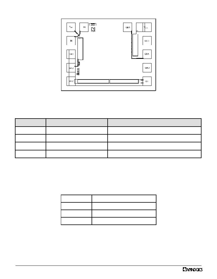
Figure 3: ATA 01504D1C Typical Bonding Diagram
APPLICATION INFORMATION
Power supplies and general layout considerations
The ATA01504D1C may be operated from a positive
supply as low as +4.5 V and as high as +6.0 V. Below
+4.5 V, bandwidth, overload and sensitivity will
degrade, while at +6.0 V, bandwidth, overload and
sensitivity. Use of surface mount (preferably MIM type
capacitors), low inductance power supply bypass
capacitors (>=56pF) are essential for good high
frequency and low noise performance. The power
supply bypass capacitors should be mounted on or
connected to a good low inductance ground plane.
General layout considerations
Since the gain stages of the transimpedance
amplifier have an open loop bandwidth in excess of
1.0 GHz, it is essential to maintain good high
frequency layout practices. To prevent oscillations, a
low inductance RF ground plane should be made
available for power supply bypassing. Traces that
can be made short should be made short, and the
utmost care should be taken to maintain very low
capacitance at the photodiode TIA interface (I
IN
), as
excess capacitance at this node will cause a
degradation in bandwidth and sensitivity (see
Bandwidth vs. C
T
curves).
Note: All performance curves are typical @ TA =25 ∞C
unless otherwise noted.
V
DD
= 4.5 V
V
DD
= 5.0 V
V
DD
= 5.5 V
210
200
190
180
170
160
150
0 0.2 0.4 0.6 0.8 1 1.2 1.4 1.6
B(3dB) A / 2
Rf (C
in
+C
t
)
C
T
(pF)
B
a
n
d
wi
t
h
(
M
Hz)
Figure 4: Bandwidth vs. CT
V
CAGC

PRELIMINARY DATA SHEET - Rev 1
08/2001
5
ATA01504
V
OUT
Connection
The output pad should be connected via a coupling
capacitor to the next stage of the receiver channel
(filter or decision circuits), as the output buffers are
not designed to drive a DC coupled 50 ohm load
(this would require an output bias current of
approximately 36 mA to maintain a quiescent 1.8
Volts across the output load). If V
OUT
is connected to a
high input impedance decision circuit (>500 ohms),
then a coupling capacitor may not be required,
although caution should be exercised since DC
offsets of the photo detector/TIA combination may
cause clipping of subsequent gain or decision
circuits.
I
IN
connection
(refer to the equivalent circuit diagram) Bonding the
detector cathode to I
IN
(and thus drawing current from
the ATA01504) improves the dynamic range. Although
the detector may be used in the reverse direction for
input currents not exceeding 25 mA, the specifications
for optical overload will not be met.
I
V
DD
= 5.5 V
V
DD
= 4.5 V
I
IN
(mA DC)
10
9
8
7
6
5
4
3
2
1
T
r
an
s
i
m
p
e
d
an
c
e
(
K
O
h
m
)
I
IN
50
-2.1 - 1.6 -1.1 - 0.6 - 0.1
V
DD
= 4.5 V
V
DD
=5.5 V
Output Collapse
I
IN
V
OUT
I
IN
(mA DC)
heavy AGC
Linear Region
V
OU
T
(V
o
l
t
s
)
R
f
3.4
3.2
3.0
2.9
2.7
2.5
2.4
2.2
2.0
1.9
1.7
1.5
1.4
1.2
1.0
0.8
0.7
0.5
0.3
0.2
0.0
- 4
- 3
- 2
- 1
Sensitivity and Bandwidth
In order to guarantee sensitivity and bandwidth
performance, the TIA is subjected to a
comprehensive series of tests at the die sort level
(100% testing at 25
o
C) to verify the DC parametric
performance and the high frequency performance
(i.e. adequate |S21|) of the amplifier. Acceptably high
|S21| of the internal gain stages will ensure low
amplifier input capacitance and hence low input
referred noise current. Transimpedance sensitivity
and bandwidth are then guaranteed by design and
correlation with RF and DC die sort test results.
Figure 5: Transimpedance vs. I
IN
0.1
0.3
0.5
0.7
0.9
1.1
1.3
1.5
V
DD
=4.5 V
V
DD
=5.5 V
50
I
IN
(mA DC)
Bandwidth vs
I
IN
I
IN
B
A
NDW
I
D
T
H
(
G
Hz
)
- 2.1 - 1.6 - 1.1 - 0.6 - 0.1
1501
Figure 6: Bandwidth vs. I
IN
Figure 7: V
OUT
vs. I
IN

PRELIMINARY DATA SHEET - Rev 1
08/2001
6
ATA01504
Indirect Measurement of Optical Overload
Optical overload can be defined as the maximum
optical power above which the BER (bit error rate)
increases beyond 1 error in 10
10
bits. The
ATA01504D1C is 100% tested at die sort by a DC
measurement which has excellent correlation with
an PRBS optical overload measurement. The
measurement consists of sinking a negative current
(see V
OUT
Vs I
IN
figure) from the TIA and determining
the point of output voltage collapse. Also the input
node virtual ground during heavy AGC is checked
to verify that the linearity (i.e. pulse width distortion)
of the amplifier has not been compromised.
Measurement of Input Referred Noise Current
The Input Noise Current is directly related to
sensitivity . It can be defined as the output noise
voltage (Vout), with no input signal, (including a 110
MHz lowpass filter at the output of the TIA) divided by
the AC transresistance.
AGC Capacitor
It is important to select an external AGC capacitor of
high quality and appropriate size. The ATA01504D1C
has an on-chip 70 KW resistor with a shunt 4 pF
capacitor to ground. Without external capacitance the
chip will provide an AGC time constant of 280 nS. For
the best performance in a typical 155 MB/s SONET
receiver, a minimum AGC capacitor of 56pF is
recommended. This will provide the minimum
amount of protection against pattern sensitivity and
pulse width distortion on repetitive data sequences
during high average optical power conditions.
Conservative design practices should be followed
when selecting an AGC capacitor, since unit to unit
variability of the internal time constant and various
data conditions can lead to data errors if the chosen
value is too small.
p
A
/
H
z
C
T
=1.0pF
CT
50
CT =0.5pF
14
10
6
2
- 0.1 1 10 100 1000
Frequency (MHz)
R
f
Phase response
At frequencies below the 3dB bandwidth of the device,
the transimpedance phase response is
characteristic of a single pole transfer function (as
shown in the Phase Vs Frequency curve). The output
impedance is essentially resistive up to 1000 MHz.
Figure 8: Input Referred Noise Spectral Density
Figure 9: Phase (I
IN
to V
OUT
)

PRELIMINARY DATA SHEET - Rev 1
08/2001
7
ATA01504
NOTES

PRELIMINARY DATA SHEET - Rev 1
08/2001
8
IMPORTANT NOTICE
ANADIGICS, Inc. reserves the right to make changes to its products or to discontinue any product at any time without
notice. The product specifications contained in Advanced Product Information sheets and Preliminary Data Sheets are
subject to change prior to a products formal introduction. Information in Data Sheets have been carefully checked and are
assumed to be reliable; however, ANADIGICS assumes no responsibilities for inaccuracies. ANADIGICS strongly urges
customers to verify that the information they are using is current before placing orders.
WARNING
ANADIGICS products are not intended for use in life support appliances, devices, or systems. Use of an ANADIGICS
product in any such application without written consent is prohibited.
ANADIGICS, Inc.
141 Mount Bethel Road
Warren, New Jersey 07059, U.S.A
Tel: +1 (908) 668-5000
Fax: +1 (908) 668-5132
http://www.anadigics.com
Mktg@anadigics.com
ATA01504
R
E
B
M
U
N
T
R
A
P
N
O
I
T
P
O
E
G
A
K
C
A
P
N
O
I
T
P
I
R
C
S
E
D
E
G
A
K
C
A
P
C
1
D
4
0
5
1
0
A
T
A
C
1
D
e
i
D
ORDERING INFORMATION