 | –≠–ª–µ–∫—Ç—Ä–æ–Ω–Ω—ã–π –∫–æ–º–ø–æ–Ω–µ–Ω—Ç: CS8281 | –°–∫–∞—á–∞—Ç—å:  PDF PDF  ZIP ZIP |
1
Features
s
5V, 250mA Primary Output
s
5V, 100mA Secondary
Output
s
3% Tolerance, Both
Outputs
s
ON/OFF Control for
Primary Output
s
Low Quiescent Current
Drain (100µA V
OUT2
)
s
Low Reverse Current
s
Protection Features
Reverse Battery (-15V)
74V Load Dump
Short Circuit
Overtemperature
Overvoltage (34V)
Package Options
CS8281
5V/250mA, 5V/100mA Micropower
Low Dropout Regulator with ENABLE
CS8281
Description
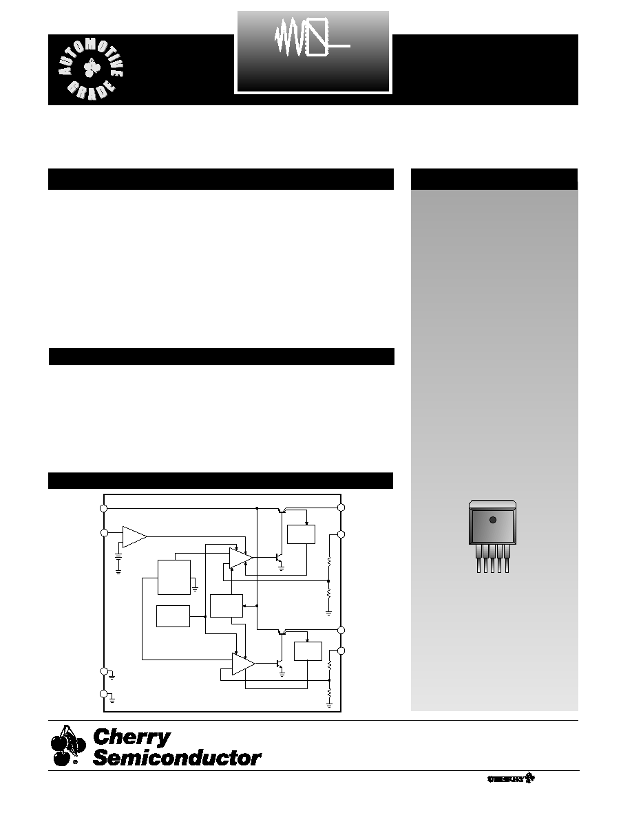
V
IN
ENABLE
+
-
Secondary Output
Primary Output
Current
Limit
Current
Limit
V
OUT1
Thermal
Shutdown
Over
Voltage
Shutdown
Bandgap
Reference
+
-
V
OUT2
+
-
V
OUT2
Sense
V
OUT1
Sense
Pwr Gnd
Gnd
Block Diagram
Absolute Maximum Ratings
Input Voltage.....................................................................................-15V to 74V
Power Dissipation .................................................................Internally Limited
Operating Temperature Range................................................-40°C to +125°C
Maximum Junction Temperature ...........................................-40°C to +150°C
Storage Temperature Range ....................................................-55°C to +150°C
Electrostatic Discharge (Human Body Model) ..........................................4kV
Lead Temperature Soldering
Reflow (SMD styles only)................16 sec. max above 183°C, 230°C peak
The CS8281 is a precision, dual 5V
micropower linear voltage regula-
tor. The switched primary output
(V
OUT1
) supplies up to 250mA
while the secondary (V
OUT2
) is
capable of supplying 100mA. Both
outputs have a maximum dropout
voltage of 600mV and low reverse
current. Quiescent current drain is
typically 150µA when supplying
100µA from each output.
The ENABLE input provides logic
level control of the primary output.
With the primary output disabled,
quiescent current drain is typically
100µA when supplying 100µA from
the secondary output.
The CS8281 is extremely robust
with protection provided for
reverse battery, short circuit, over-
voltage, and overtemperature on
both outputs.
The CS8281 is available in a 5-lead
D
2
PAK.
5 Lead D
2
PAK
Tab (Gnd)
1
Consult factory for 8L and 16L SO, 8L and
16L PDIP, 7L D
2
PAK and 5L TO-220.
1. V
IN
2. V
OUT1
3. Gnd
4. V
OUT2
5. ENABLE
A Company
®
Cherry Semiconductor Corporation
2000 South County Trail, East Greenwich, RI 02818
Tel: (401)885-3600 Fax: (401)885-5786
Email: info@cherry-semi.com
Web Site: www.cherry-semi.com
Rev. 9/16/97

2
CS8281
PARAMETER
TEST CONDITIONS
MIN
TYP
MAX
UNIT
Electrical Characteristics: 6V ≤ V
IN
≤ 26V, I
OUT1
= I
OUT2
= 100µA, -40°C ≤ T
C
≤ 125˚C unless otherwise specified
s Primary Output Stage (V
OUT1
)
Output Voltage, V
OUT1
100µA ≤ I
OUT1
≤ 250mA
4.85
5.00
5.15
V
Dropout Voltage
I
OUT1
= 250mA
400
600
mV
I
OUT1
= 100µA
100
150
mV
Line Regulation
6V ≤ V
IN
≤ 26V
5
50
mV
Load Regulation
1mA ≤ I
OUT1
≤ 250mA, V
IN
= 14V
5
50
mV
Quiescent Current
ENABLE = HIGH, V
IN
= 16V,
22
50
mA
I
OUT1
= 250mA
Ripple Rejection
f = 120Hz, I
OUT1
= 125mA, 7V ≤ V
IN
≤ 17V
60
70
dB
Current Limit
260
400
mA
Short Circuit Current Limit
V
OUT1
= 0V, V
IN
= 16V
25
mA
Reverse Current
V
OUT1
= 5V, V
IN
= 0V
100
1500
µA
s Secondary Output (V
OUT2
)
Output Voltage, V
OUT2
100µA ≤ I
OUT2
≤ 100mA
4.85
5.00
5.15
V
Dropout Voltage
I
OUT2
= 100mA
400
600
mV
I
OUT2
= 100µA
100
150
mV
Line Regulation
6V ≤ V
IN
≤ 26V
5
50
mV
Load Regulation
100µA ≤ I
OUT2
≤ 100mA, V
IN
= 14V
5
50
mV
Quiescent Current
ENABLE = LOW, V
IN
= 12.8V
100
150
µA
ENABLE = HIGH, V
IN
= 16V,
8
25
mA
I
OUT2
= 100mA
Ripple Rejection
f = 120Hz, I
OUT2
= 50mA, 7V ≤ V
IN
≤ 17V
60
70
dB
Current Limit
105
200
mA
Short Circuit Current Limit
V
OUT2
= 0V, V
IN
= 16V, I
OUT1
= 0A
25
mA
Reverse Current
V
OUT2
= 5V, V
IN
= 0V
100
250
µA
s Enable Function (ENABLE)
Input Threshold
ENABLE = LOW, 7V ≤ V
IN
≤ 26V
1.2
0.8
V
ENABLE = HIGH, 7V ≤ V
IN
≤ 26V
2.0
1.2
V
Input Bias Current
0V ≤ V
ENABLE
≤ 5V
-2
0
2
µA
s Protection Circuits
Overtemperature Threshold
150
180
°C
Overvoltage Shutdown
30
34
38
V

Definition of Terms
3
CS8281
V
IN
ENABLE
V
OUT
1
System
Condition
60V
3V
2.4V
5V
0V
Turn
On
Load
Dump
Low V
IN
Line Noise, Etc.
V
OUT2
Short
Circuit
Thermal
Shutdown
Turn
Off
5V
0V
14V
5V
2.0V
0.8V
14V
26V
31V
5V
5V
2.4V
5V
5V
5V
0V
V
OUT
2
5V
5V
0V
5V
V
OUT
1
Short
Circuit
0V
5V
5V
Typical Circuit Waveform
PACKAGE LEAD #
LEAD SYMBOL
FUNCTION
Package Lead Description
5 Lead D
2
PAK
1
V
IN
Supply voltage to IC, usually direct from battery.
2
V
OUT1
5V regulated output which is activated by ENABLE input.
3
Gnd
Ground connection.
4
V
OUT2
Standby output 5V, 100mA capability; always on.
5
ENABLE
CMOS compatible input lead; switches V
OUT1
. When ENABLE is
high, V
OUT1
is active.
Current Limit
Peak current that can be delivered to the output.
Dropout Voltage
The input-output voltage differential at which the circuit
ceases to regulate against further reduction in input volt-
age. Measured when the output voltage has dropped
100mV from the nominal value obtained at 14V input,
dropout voltage is dependent upon load current and junc-
tion temperature.
Input Output Differential
The voltage difference between the unregulated input volt-
age and the regulated output voltage for which the regula-
tor will operate.
Input Voltage
The DC voltage applied to the input terminals with respect
to ground.
Line Regulation
The change in output voltage for a change in the input
voltage. The measurement is made under conditions of
low dissipation or by using pulse techniques such that the
average chip temperature is not significantly affected.
Load Regulation
The change in output voltage for a change in load current
at constant chip temperature.
Long Term Stability
Output voltage stability under accelerated life-test condi-
tions after 1000 hours with maximum rated voltage and
junction temperature.
Quiescent Current
The part of the positive input current that does not con-
tribute to the positive load current. i.e., the regulator
ground lead current.
Ripple Rejection
The ratio of the peak-to-peak input ripple voltage to the
peak-to-peak output ripple voltage.
Short Circuit Current Limit
Peak current that can be delivered by the output when
forced to 0V.
Temperature Stability of V
OUT
The percentage change in output voltage for a thermal varia-
tion from room temperature to either temperature extreme.

The CS8281 is a micropower dual 5V regulator. All bias
required to operate the internal circuitry is derived from
the standby output, V
OUT2
. If this output experiences an
over current situation and collapses, then V
OUT1
will also
collapse (see timing diagrams).
If there is critical circuitry that must remain active under
most conditions it should be connected to V
OUT2
. Any cir-
cuitry that is likely to be subjected to a short circuit, e.g.,
circuitry outside the module, should be connected to V
OUT1
.
Output capacitors are required for stability with the CS8281.
Without them, the regulator outputs will oscillate. Actual
size and type may vary depending upon the application
load and temperature range. Capacitor effective series
resistance (ESR) is also a factor in the IC stability. Worst-
case is determined at the minimum ambient temperature
and maximum load expected.
Output capacitors can be increased in size to any desired
value above the minimum. One possible purpose of this
would be to maintain the output voltages during brief con-
ditions of negative input transients that might be character-
istic of a particular system.
Capacitors must also be rated at all ambient temperatures
expected in the system. To maintain regulator stability
down to -40˚C, capacitors rated at that temperature must be
used.
More information on capacitor selection for Smart
Regulators™ is available in the Smart Regulator applica-
tion note, Compensation for Linear Regulators.
The ENABLE function controls V
OUT1
. When ENABLE is
high, V
OUT1
is on. When ENABLE is low, V
OUT1
is off.
The maximum power dissipation for a dual output regula-
tor (Figure 1) is:
PD(max) = {V
IN
(max)–V
OUT1
(min)}I
OUT1
(max)+
{V
IN
(max)–V
OUT2
(min)}I
OUT2
(max)+V
IN
(max)I
Q
(1)
where:
V
IN
(max) is the maximum input voltage,
V
OUT1
(min) is the minimum output voltage from V
OUT1
,
V
OUT2
(min) is the minimum output voltage from V
OUT2
,
I
OUT1
(max) is the maximum output current for the appli-
cation,
I
OUT2
(max) is the maximum output current for the appli-
cation, and
I
Q
is the quiescent current the regulator consumes at both
I
OUT1
(max) and I
OUT2
(max).
Once the value of PD(max) is known, the maximum per-
missible value of R
QJA
can be calculated:
R
QJA
=
(2)
The value of R
QJA
can then be compared with those in
the package section of the data sheet. Those packages with
R
QJA
's less than the calculated value in equation 2 will keep
the die temperature below 150°C.
In some cases, none of the packages will be sufficient to
dissipate the heat generated by the IC, and an external heat
sink will be required.
Figure 1: Dual output regulator with key performance parameters
labeled.
A heat sink effectively increases the surface area of the
package to improve the flow of heat away from the IC and
into the surrounding air.
Each material in the heat flow path between the IC and the
outside environment will have a thermal resistance. Like
series electrical resistances, these resistances are summed to
determine the value of R
QJA
.
R
QJA
= R
QJC
+ R
QCS
+ R
QSA
(3)
where:
R
QJC
= the junction–to–case thermal resistance,
R
QCS
= the case–to–heat sink thermal resistance, and
R
QSA
= the heat sink–to–ambient thermal resistance.
R
QJC
appears in the package section of the data sheet. Like
R
QJA
, it too is a function of package type. R
QCS
and R
QSA
are
functions of the package type, heat sink and the interface
between them. These values appear in heat sink data sheets
of heat sink manufacturers.
Heat Sinks
V
IN
V
OUT
2
I
IN
I
Q
Control
Features
}
I
OUT
2
V
OUT
1
I
OUT
1
Smart
Regulator
150°C - T
A
P
D
Calculating Power Dissipation
in a Dual Output Linear Regulator
ENABLE
External Capacitors
General
4
CS8281
Application Notes

5
CS8281
Test & Application Circuit
ENABLE
V
IN
V
OUT1
CS8281
Gnd
22
mF
ESR<8
W
V
CC
I/O
m
P
Gnd
Load
0.1
mF
V
BATT
C
2
C
1
C
3
V
OUT2
22
mF
ESR<8
W
* C1 required if regulator is located far from power supply filter.
** C2 and C3 required for stability. Capacitor must operate at minimum temperature expected during system operations.