1
Preliminary
Preliminary
EDS-101101 Rev D
Product Description
522 Almanor Ave., Sunnyvale, CA 94085 Phone: (800) SMI-MMIC http://www.sirenza.com
The information provided herein is believed to be reliable at press time. Sirenza Microdevices assumes no responsibility for inaccuracies or omissions. Sirenza Microdevices assumes no responsibility for the use of
this information, and all such information shall be entirely at the users own risk. Prices and specifications are subject to change without notice. No patent rights or licenses to any of the circuits described herein are
implied or granted to any third party. Sirenza Microdevices does not authorize or warrant any Sirenza Microdevices product for use in life-support devices and/or systems. Copyright 2001 Sirenza Microdevices, Inc..
All worldwide rights reserved.
0
5
10
15
20
25
0
1
2
3
4
5
6
7
8
NGA-186
DC-6000 MHz, Cascadable GaAs
HBT MMIC Amplifier
Product Features
12.0dB Gain, 14.7 dBm P1dB at 1950Mhz
Cascadable 50 ohm: 1.2:1 VSWR
Patented GaAs HBT Technology
Operates from Single Supply
Low Thermal Resistance Package
Unconditionally Stable
Applications
PA Driver Amplifier
Cellular, PCS, GSM, UMTS
IF Amplifier
Wireless Data, Satellite
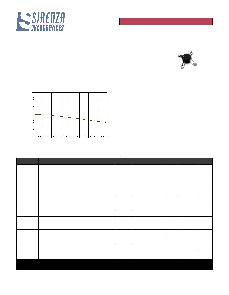
dB
Small Signal Gain vs. Frequency
Sirenza Microdevices NGA-186 is a high performance Gallium
Arsenide Heterojunction Bipolar Transistor MMIC Amplifier. De-
signed with InGaP process technology for improved reliability, a
Darlington configuration is utilized for broadband performance up
to 6 Ghz. The heterojunction increases breakdown voltage and
minimizes leakage current between junctions. Cancellation of
emitter junction non-linearities results in higher suppression of
intermodulation products.
Frequency GHz
l
o
b
m
y
S
r
e
t
e
m
a
r
a
P
s
t
i
n
U
y
c
n
e
u
q
e
r
F
.
n
i
M
.
p
y
T
.
x
a
M
P
B
d
1
n
o
i
s
s
e
r
p
m
o
C
B
d
1
t
a
r
e
w
o
P
t
u
p
t
u
O
m
B
d
z
H
M
0
5
8
z
H
M
0
5
9
1
z
H
M
0
0
4
2
6
.
4
1
7
.
4
1
9
.
4
1
P
I
O
3
t
n
i
o
P
t
p
e
c
r
e
t
n
I
r
e
d
r
O
d
r
i
h
T
t
u
p
t
u
O
m
B
d
z
H
M
0
5
8
z
H
M
0
5
9
1
z
H
M
0
0
4
2
9
.
2
3
7
.
1
3
1
.
1
3
G
n
i
a
G
l
a
n
g
i
S
ll
a
m
S
B
d
z
H
M
0
5
8
z
H
M
0
5
9
1
z
H
M
0
0
4
2
2
.
1
1
4
.
2
1
0
.
2
1
8
.
1
1
6
.
3
1
h
t
d
i
w
d
n
a
B
)
B
d
0
1
-
<
(
s
s
o
L
n
r
u
t
e
R
y
b
d
e
n
i
m
r
e
t
e
D
z
H
M
0
0
6
5
R
W
S
V
t
u
p
n
I
-
z
H
M
0
0
0
5
-
C
D
1
:
2
.
1
R
W
S
V
t
u
p
t
u
O
-
z
H
M
0
0
0
5
-
C
D
1
:
2
.
1
F
N
e
r
u
g
i
F
e
s
i
o
N
B
d
z
H
M
0
0
0
2
0
.
4
V
D
e
g
a
tl
o
V
g
n
it
a
r
e
p
O
e
c
i
v
e
D
V
6
.
3
1
.
4
6
.
4
I
D
t
n
e
r
r
u
C
g
n
it
a
r
e
p
O
e
c
i
v
e
D
A
m
5
4
0
5
5
5
R
H
T
l-
j
,
)
d
a
e
l
o
t
n
o
it
c
n
u
j
(
e
c
n
a
t
s
i
s
e
R
l
a
m
r
e
h
T
W
/
C
°
0
2
1
Test Conditions:
V
S
= 8 V
I
D
= 50 mA Typ.
OIP
3
Tone Spacing = 1 MHz, Pout per tone = 0 dBm
R
BIAS
= 75 Ohms
T
L
= 25ºC
Z
S
= Z
L
= 50 Ohms
2
Preliminary
EDS-101101 Rev D
NGA-186 DC-6.0 GHz 4.1V GaAs HBT
Preliminary
522 Almanor Ave., Sunnyvale, CA 94085 Phone: (800) SMI-MMIC http://www.sirenza.com
r
e
t
e
m
a
r
a
P
l
a
c
i
p
y
T
C
º
5
2
ti
n
U
n
o
it
i
d
n
o
C
t
s
e
T
I(
D
)
d
e
t
o
n
e
s
i
w
r
e
h
t
o
s
s
e
l
n
u
,
A
m
0
5
=
z
H
M
0
0
5
ni
a
G
3
P
I
t
u
p
t
u
O
B
d
1
P
t
u
p
t
u
O
s
s
o
L
n
r
u
t
e
R
t
u
p
n
I
n
oi
t
al
o
s
I
5
.
2
1
6
.
2
3
7
.
4
1
1
.
0
3
5
.
6
1
B
d
m
B
d
m
B
d
B
d
B
d
m
B
d
0
=
e
n
o
t
r
e
p
t
u
o
P
,z
H
M
1
=
g
ni
c
a
p
s
e
n
o
T
z
H
M
0
5
8
ni
a
G
3
P
I
t
u
p
t
u
O
B
d
1
P
t
u
p
t
u
O
s
s
o
L
n
r
u
t
e
R
t
u
p
n
I
n
oi
t
al
o
s
I
4
.
2
1
9
.
2
3
6
.
4
1
9
.
9
2
5
.
6
1
B
d
m
B
d
m
B
d
B
d
B
d
m
B
d
0
=
e
n
o
t
r
e
p
t
u
o
P
,z
H
M
1
=
g
ni
c
a
p
s
e
n
o
T
z
H
M
0
5
9
1
ni
a
G
3
P
I
t
u
p
t
u
O
B
d
1
P
t
u
p
t
u
O
s
s
o
L
n
r
u
t
e
R
t
u
p
n
I
n
oi
t
al
o
s
I
0
.
2
1
7
.
1
3
7
.
4
1
6
.
7
2
4
.
6
1
B
d
m
B
d
m
B
d
B
d
B
d
m
B
d
0
=
e
n
o
t
r
e
p
t
u
o
P
,z
H
M
1
=
g
ni
c
a
p
s
e
n
o
T
z
H
M
0
0
4
2
ni
a
G
3
P
I
t
u
p
t
u
O
B
d
1
P
t
u
p
t
u
O
s
s
o
L
n
r
u
t
e
R
t
u
p
n
I
n
oi
t
al
o
s
I
8
.
1
1
1
.
1
3
9
.
4
1
3
.
5
2
4
.
6
1
B
d
m
B
d
m
B
d
B
d
B
d
m
B
d
0
=
e
n
o
t
r
e
p
t
u
o
P
,z
H
M
1
=
g
ni
c
a
p
s
e
n
o
T
Key parameters, at typical operating frequencies:
Absolute Maximum Ratings
r
e
t
e
m
a
r
a
P
ti
m
i
L
e
t
u
l
o
s
b
A
.
x
a
M
t
n
e
r
r
u
C
e
c
i
v
e
D
I(
D
)
1
0
1
A
m
.
x
a
M
e
c
i
v
e
D
V
(
e
g
a
tl
o
V
D
)
V
6
.
x
a
M
r
e
w
o
P
t
u
p
n
I
F
R
m
B
d
0
1
+
.
x
a
M
p
m
e
T
n
o
it
c
n
u
J
T
(
.
J
)
C
°
0
5
1
+
p
m
e
T
g
n
it
a
r
e
p
O
T
(
e
g
n
a
R
.
L
)
C
°
5
8
+
o
t
C
°
0
4
-
.
x
a
M
p
m
e
T
e
g
a
r
o
t
S
.
C
°
0
5
1
+
y
a
m
s
ti
m
il
e
s
e
h
t
f
o
e
n
o
y
n
a
d
n
o
y
e
b
e
c
i
v
e
d
s
i
h
t
f
o
n
o
it
a
r
e
p
O
,
n
o
it
a
r
e
p
o
s
u
o
n
it
n
o
c
e
l
b
a
il
e
r
r
o
F
.
e
g
a
m
a
d
t
n
e
n
a
m
r
e
p
e
s
u
a
c
m
u
m
i
x
a
m
e
h
t
d
e
e
c
x
e
t
o
n
t
s
u
m
t
n
e
r
r
u
c
d
n
a
e
g
a
tl
o
v
e
c
i
v
e
d
e
h
t
.
e
n
o
e
g
a
p
n
o
e
l
b
a
t
e
h
t
n
i
d
e
if
i
c
e
p
s
s
e
u
l
a
v
g
n
it
a
r
e
p
o
:
n
o
i
s
s
e
r
p
x
e
g
n
i
w
o
ll
o
f
e
h
t
y
f
s
it
a
s
o
s
l
a
d
l
u
o
h
s
s
n
o
it
i
d
n
o
C
s
a
i
B
I
D
V
D
T
(
<
J
T
-
L
R
/
)
H
T
l-
j
,

3
Preliminary
EDS-101101 Rev D
NGA-186 DC-6.0 GHz 4.1V GaAs HBT
Preliminary
522 Almanor Ave., Sunnyvale, CA 94085 Phone: (800) SMI-MMIC http://www.sirenza.com
-35
-30
-25
-20
-15
-10
-5
0
0
1
2
3
4
5
6
7
8
-35
-30
-25
-20
-15
-10
-5
0
0
1
2
3
4
5
6
7
8
-35
-30
-25
-20
-15
-10
-5
0
0
1
2
3
4
5
6
7
8
0
5
10
15
20
25
0
1
2
3
4
5
6
7
8
dB
S12, I
D
=50mA, T=25ºC
S22, I
D
=50mA, T=25ºC
dB
Frequency GHz
Frequency GHz
dB
S11, I
D
=50mA, T=25ºC
Frequency GHz
S21, I
D
=50mA, T=25ºC
dB
Frequency GHz
Electrical Specifications at Ta = 25ºC
4
Preliminary
EDS-101101 Rev D
NGA-186 DC-6.0 GHz 4.1V GaAs HBT
Preliminary
522 Almanor Ave., Sunnyvale, CA 94085 Phone: (800) SMI-MMIC http://www.sirenza.com
e
c
n
e
r
e
f
e
R
r
o
t
a
n
g
i
s
e
D
)
z
h
M
(
y
c
n
e
u
q
e
r
F
0
0
5
0
5
8
0
5
9
1
0
0
4
2
0
0
5
3
C
B
F
p
0
2
2
F
p
0
0
1
F
p
8
6
F
p
6
5
F
p
9
3
C
D
F
p
0
0
1
F
p
8
6
F
p
2
2
F
p
2
2
F
p
5
1
L
C
H
n
8
6
H
n
3
3
H
n
2
2
H
n
8
1
H
n
5
1
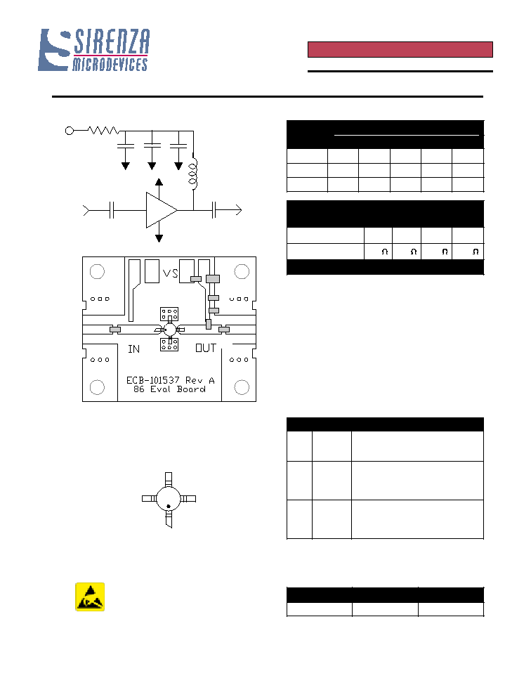
Mounting Instructions
1. Use a large ground pad area under device pins 2
and 4 with many plated through-holes as shown.
2. We recommend 1 or 2 ounce copper. Measurements
for this data sheet were made on a 31 mil thick FR-4
board with 1 ounce copper on both sides.
Basic Application Circuit
RF in
RF out
1 uF
C
B
C
B
C
D
V
S
R
BIAS
L
C
1
2
3
4
1000
pF
NGA-186
Application Circuit Element Values
Part Number Ordering Information
r
e
b
m
u
N
t
r
a
P
e
z
i
S
l
e
e
R
l
e
e
R
/
s
e
c
i
v
e
D
6
8
1
-
A
G
N
"
7
0
0
0
1
The part will be marked with an N1 designator on
the top surface of the package.
Part Identification Marking
#
n
i
P
n
o
it
c
n
u
F
n
o
it
p
i
r
c
s
e
D
1
N
I
F
R
e
s
u
e
h
t
s
e
ri
u
q
e
r
n
i
p
s
i
h
T
.
n
i
p
t
u
p
n
i
F
R
r
o
ti
c
a
p
a
c
g
n
i
k
c
o
l
b
C
D
l
a
n
r
e
t
x
e
n
a
f
o
.
n
o
it
a
r
e
p
o
f
o
y
c
n
e
u
q
e
rf
e
h
t
r
o
f
n
e
s
o
h
c
4
,
2
D
N
G
s
e
l
o
h
a
i
v
e
s
U
.
d
n
u
o
r
g
o
t
n
o
it
c
e
n
n
o
C
d
a
e
l
e
c
u
d
e
r
o
t
e
c
n
a
m
r
o
fr
e
p
t
s
e
b
r
o
f
s
a
s
d
a
e
l
d
n
u
o
r
g
o
t
e
s
o
l
c
s
a
e
c
n
a
t
c
u
d
n
i
.
e
l
b
i
s
s
o
p
3
/
T
U
O
F
R
S
A
I
B
s
i
e
g
a
tl
o
v
C
D
.
n
i
p
s
a
i
b
d
n
a
t
u
p
t
u
o
F
R
C
D
a
e
r
o
f
e
r
e
h
t
,
n
i
p
s
i
h
t
n
o
t
n
e
s
e
r
p
r
o
f
y
r
a
s
s
e
c
e
n
s
i
r
o
ti
c
a
p
a
c
g
n
i
k
c
o
l
b
.
n
o
it
a
r
e
p
o
r
e
p
o
r
p
Caution: ESD sensitive
Appropriate precautions in handling, packaging and
testing devices must be observed.
1 uF
R
BIAS
N1
1000 pF
C
B
C
B
C
D
L
C
V
S
1
2
3
4
N1
I
r
o
f
s
e
u
l
a
V
r
o
t
s
i
s
e
R
s
a
i
B
d
e
d
n
e
m
m
o
c
e
R
D
A
m
0
5
=
R
S
A
I
B
V
(
=
S
V
-
D
I
/
)
D
V
(
e
g
a
tl
o
V
yl
p
p
u
S
S
)
V
6
V
8
V
0
1
V
2
1
R
S
A
I
B
9
3
5
7
0
2
1
0
6
1
R
:
e
t
o
N
S
A
I
B
.
e
r
u
t
a
r
e
p
m
e
t
r
e
v
o
y
ti
li
b
a
t
s
s
a
i
b
C
D
s
e
d
iv
o
r
p

5
Preliminary
EDS-101101 Rev D
NGA-186 DC-6.0 GHz 4.1V GaAs HBT
Preliminary
522 Almanor Ave., Sunnyvale, CA 94085 Phone: (800) SMI-MMIC http://www.sirenza.com
PCB Pad Layout
Dimensions in inches [millimeters]
Nominal Package Dimensions
Dimensions in inches [millimeters]
Refer to drawing posted at www.sirenza.com for tolerances.