 | –≠–ª–µ–∫—Ç—Ä–æ–Ω–Ω—ã–π –∫–æ–º–ø–æ–Ω–µ–Ω—Ç: AD7305 | –°–∫–∞—á–∞—Ç—å:  PDF PDF  ZIP ZIP |

REV. A
Information furnished by Analog Devices is believed to be accurate and
reliable. However, no responsibility is assumed by Analog Devices for its
use, nor for any infringements of patents or other rights of third parties
which may result from its use. No license is granted by implication or
otherwise under any patent or patent rights of Analog Devices.
a
AD7304/AD7305*
One Technology Way, P.O. Box 9106, Norwood, MA 02062-9106, U.S.A.
Tel: 781/329-4700
World Wide Web Site: http://www.analog.com
Fax: 781/326-8703
© Analog Devices, Inc., 1998
FUNCTIONAL BLOCK DIAGRAMS
PWR ON
RESET
V
SS
AD7304
V
OUT
A
V
OUT
B
INPUT
REG A
DAC A
CS
LDAC
SDI/SHDN
GND
CLK
8
8
8
8
DAC A
REG
DAC B
DAC B
REG
INPUT
REG B
8
INPUT
REG C
8
8
8
8
DAC C
REG
DAC D
DAC D
REG
INPUT
REG D
DAC C
SERIAL
REG
V
REF
B V
REF
A
V
OUT
C
V
OUT
D
CLR
V
REF
C V
REF
D
V
DD
PWR ON
RESET
V
SS
V
OUT
A
V
OUT
B
INPUT
REG A
DAC A
WR
LDAC
A0/SHDN
GND
A1
8
8
8
8
DAC A
REG
DAC B
DAC B
REG
8
8
8
8
8
DAC C
REG
DAC D
DAC D
REG
DAC C
V
REF
V
OUT
C
V
OUT
D
V
DD
INPUT
REG B
INPUT
REG C
INPUT
REG D
DECODE
DB0
DB1
DB2
DB3
DB4
DB5
DB6
AD7305
FEATURES
Four 8-Bit DACs in One Package
+3 V, +5 V and 5 V Operation
Rail-to-Rail REF-Input to Voltage Output Swing
2.6 MHz Reference Multiplying Bandwidth
Compact 1.1 mm Height TSSOP 16-/20-Lead Package
Internal Power ON Reset
SPI Serial Interface Compatible--AD7304
Fast Parallel Interface--AD7305
40 A Power Shutdown
APPLICATIONS
Automotive Output Span Voltage
Instrumentation, Digitally Controlled Calibration
Pin-Compatible AD7226 Replacement when V
DD
< 5.5 V
GENERAL DESCRIPTION
The AD7304/AD7305 are quad, 8-bit DACs that operate from a
single +3 V to +5 V supply or
±5 V supplies. The AD7304 has a
serial interface, while the AD7305 has a parallel interface. Inter-
nal precision buffers swing rail-to-rail. The reference input range
includes both supply rails allowing for positive or negative full-
scale output voltages. Operation is guaranteed over the supply
voltage range of +2.7 V to +5.5 V, consuming less than 9 mW
from a +3 V supply.
The full-scale voltage output is determined by the external refer-
ence input voltage applied. The rail-to-rail V
REF
input to DAC
V
OUT
allows for a full-scale voltage set equal the positive supply
V
DD
, the negative supply V
SS
or any value in between.
The AD7304's doubled-buffered serial-data interface offers high
speed, three-wire, SPI and microcontroller compatible inputs
using data in (SDI), clock (CLK) and chip select (CS) pins.
Additionally, an internal power-on reset sets the output to zero
scale.
The parallel input AD7305 uses a standard address decode
along with the WR control line to load data into the input regis-
ters. The double buffered architecture allows all four input
registers to be preloaded with new values, followed by a LDAC
control strobe which copies all the new data into the DAC regis-
ters thereby updating the analog output values. When operating
from less than +5.5 V, the AD7305 is pin-compatible with the
popular industry standard AD7226.
An internal power ON reset places both parts in the zero-scale
state at turn ON. A 40
µA power shutdown (SHDN) feature is
activated on both parts by tristating the SDI/SHDN pin on the
AD7304, and tristating the A0/SHDN address pin on the
AD7305.
The AD7304/AD7305 are specified over the extended industrial
(≠40
∞C to +85∞C), and the automotive (≠40∞C to +125∞C)
temperature ranges. AD7304s are available in 16-lead plastic
DIP (N-16), and wide-body SOL-16 (R-16) packages. The
parallel input AD7305 is available in the 20-lead plastic DIP
(N-20), and the SOL-20 (R-20) surface mount package. For
ultracompact applications the thin 1.1 mm TSSOP-16 (RU-16)
package will be available for the AD7304, while the TSSOP-20
(RU-20) will house the AD7305.
*Protected under Patent Number 5684481.
+3 V/+5 V, Rail-to-Rail
Quad, 8-Bit DAC

≠2≠
REV. A
AD7304/AD7305≠SPECIFICATIONS
(@ V
DD
= +3 V or +5 V, V
SS
= 0 V; or V
DD
= +5 V and V
SS
= ≠5 V, V
SS
V
REF
V
DD
, ≠40 C < T
A
< +85 C/+125 C, unless otherwise noted.)
Parameter
Symbol
Condition
3 V 10% 5 V 10%
5 V 10%
Units
STATIC PERFORMANCE
Resolution
1
N
8
8
8
Bits
Integral Nonlinearity
2
INL
±1
±1
±1
LSB max
Differential Nonlinearity
DNL
Monotonic, All Codes 0 to FF
H
±1
±1
±1
LSB max
Zero-Scale Error
V
ZSE
Data = 00
H
15
15
±15
mV max
Full-Scale Voltage Error
V
FSE
Data = FF
H
±4
±4
±4
LSB max
Full-Scale Tempco
3
TCV
FS
5
5
5
ppm/
∞C typ
4
REFERENCE INPUT
V
REFIN
Range
V
REFIN
V
SS
/V
DD
V
SS
/V
DD
V
SS
/V
DD
V min/max
Input Resistance (AD7304)
R
REFIN
Code = 55
H
28
28
28
k
typ
Input Resistance (AD7305)
R
REFIN
All DACs at Code = 55
H
7.5
7.5
7.5
k
typ
Input Capacitance
3
C
REFIN
5
5
5
pF typ
ANALOG OUTPUTS
Output Voltage Range
V
OUT
V
SS
/V
DD
V
SS
/V
DD
V
SS
/V
DD
V min/max
Output Current Drive
I
OUT
Code = 80
H
,
V
OUT
< 1 LSB
±3
±3
±3
mA typ
Shutdown Resistance
R
OUT
DAC Outputs Placed in Shutdown State 120
120
120
k
typ
Capacitive Load
3
C
L
No Oscillation
200
200
200
pF typ
LOGIC INPUTS
Logic Input Low Voltage
V
IL
0.6
0.8
0.8
V min
Logic Input High Voltage
V
IH
2.1
2.4
2.4
V max
Input Leakage Current
5
I
IL
±10
±10
±10
µA max
Input Capacitance
3
C
IL
8
8
8
pF max
AC CHARACTERISTICS
3
Output Slew Rate
SR
Code = 00
H
to FF
H
to 00
H
1/2.7
1/3.6
1/3.6
V/
µs min/typ
Reference Multiplying
BW
Small Signal, V
SS
= ≠5 V
2.6
MHz typ
Total Harmonic Distortion
THD
V
REF
= 4 V p-p, V
SS
= ≠5 V, f = 1 kHz
0.025
%
Settling Time
6
t
S
To
±0.1% of Full Scale
1.1/2
1.0/2
1.0/2
µs typ/max
Shutdown Recovery Time
t
SDR
To
±0.1% of Full Scale
2
2
2
µs max
Time to Shutdown
t
SDN
15
15
15
µs typ
DAC Glitch
Q
15
15
15
nVs typ
Digital Feedthrough
Q
2
2
2
nVs typ
Feedthrough
V
OUT
/V
REF
Code = 00
H
, V
REF
=1 V p-p, f = 100 kHz
≠65
dB
SUPPLY CHARACTERISTICS
Positive Supply Current
I
DD
V
LOGIC
= 0 V or V
DD
, No Load
6
6
6
mA max
Negative Supply Current
I
SS
V
SS
= ≠5 V
6
mA max
Power Dissipation
P
DISS
V
LOGIC
= 0 V or V
DD
, No Load
15
30
60
mW max
Power Down
I
DD_SD
SDI/SHDN = Floating
40
40
40
µA typ
Power Supply Sensitivity
PSS
V
DD
=
±10%
0.004
0.004
0.004
%/%
NOTES
1
One LSB = V
REF
/256.
2
The first three codes (00
H
, 01
H
, 10
H
) are excluded from the integral nonlinearity error measurement in single supply operation +3 V or +5 V.
3
These parameters are guaranteed by design and not subject to production testing.
4
Typicals represent average readings measured at +25
∞C.
5
SDI/SHDN and A0/SHDN pins have 30
µA maximum I
IL
input leakage current.
6
The settling time specification does not apply for negative going transitions within the last 3 LSBs of ground in single supply operation.
Specifications subject to change without notice.
V
OUT
= 10V p-p
5V
0V
≠5V
5V
0V
≠5V
(OUT)
(IN)
V
REF
= 10V p-p
f = 20kHz
Figure 1. AD7304/AD7305 Rail-to-Rail Reference Input to Output at 20 kHz

≠3≠
AD7304/AD7305
REV. A
TIMING SPECIFICATIONS
(@ V
DD
= +3 V or +5 V, V
SS
= 0 V; or V
DD
= +5 V and V
SS
= ≠5 V, V
SS
V
REF
V
DD
, ≠40 C < T
A
<
+85 C/125 C, unless otherwise noted.)
Parameter
Symbol
3 V
10%
5 V 10%
5 V 10%
Units
INTERFACE TIMING SPECIFICATIONS
1, 2
AD7304 Only
Clock Width High
t
CH
70
55
55
ns min
Clock Width Low
t
CL
70
55
55
ns min
Data Setup
t
DS
50
40
40
ns min
Data Hold
t
DH
30
20
20
ns min
Load Pulsewidth
t
LDW
70
60
60
ns min
Load Setup
t
LD1
40
30
30
ns min
Load Hold
t
LD2
40
30
30
ns min
Clear Pulsewidth
t
CLWR
60
60
60
ns min
Select
t
CSS
30
20
20
ns min
Deselect
t
CSH
60
40
40
ns min
AD7305 Only
Data Setup
t
DS
60
40
40
ns min
Data Hold
t
DH
30
20
20
ns min
Address Setup
t
AS
60
40
40
ns min
Address Hold
t
AH
30
20
20
ns min
Write Width
t
WR
60
50
50
ns min
Load Pulsewidth
t
LDW
60
50
50
ns min
Load Setup
t
LS
60
40
40
ns min
Load Hold
t
LH
30
20
20
ns min
NOTES
1
These parameters are guaranteed by design and not subject to production testing.
2
All input control signals are specified with t
R
= t
F
= 2 ns (10% to 90% of V
DD
) and timed from a voltage level of 1.6 V.
ABSOLUTE MAXIMUM RATINGS*
V
DD
to GND . . . . . . . . . . . . . . . . . . . . . . . . . . . . ≠0.3 V, +8 V
V
SS
to GND . . . . . . . . . . . . . . . . . . . . . . . . . . . . . +0.3 V, ≠8 V
V
REFX
to GND . . . . . . . . . . . . . . . . . . . . . . . . . . . . . . V
SS
, V
DD
Logic Inputs to GND . . . . . . . . . . . . . . . ≠0.3 V, V
DD
+ 0.3 V
V
OUTX
to GND . . . . . . . . . . . . . . . . . . . . ≠0.3 V, V
DD
+ 0.3 V
I
OUT
Short Circuit to GND . . . . . . . . . . . . . . . . . . . . . 50 mA
Package Power Dissipation . . . . . . . . . . . . . . (T
J
MAX
≠T
A
)/
JA
Thermal Resistance
JA
16-Lead Plastic DIP Package (N-16) . . . . . . . . . . 103
∞C/W
16-Lead SOIC Package (R-16) . . . . . . . . . . . . . . . 73
∞C/W
TSSOP-16 Package (RU-16) . . . . . . . . . . . . . . . . 180
∞C/W
20-Lead Plastic DIP Package (N-20) . . . . . . . . . . 120
∞C/W
20-Lead SOIC Package (R-20) . . . . . . . . . . . . . . . 74
∞C/W
TSSOP-20 Package (RU-20) . . . . . . . . . . . . . . . . 155
∞C/W
Maximum Junction Temperature (T
J
MAX
) . . . . . . . . . +150
∞C
Operating Temperature Range . . . . . . . . . . . ≠40
∞C to +85∞C
Storage Temperature Range . . . . . . . . . . . . ≠65
∞C to +150∞C
Lead Temperature
N-16 and N-20 (Soldering, 10 secs) . . . . . . . . . . . . +300
∞C
R-16, R-20, RU-16, RU-20 (Vapor Phase, 60 secs) . . +215
∞C
R-16, R-20, RU-16, RU-20 (Infrared, 15 secs) . . . . +220
∞C
*Stresses above those listed under Absolute Maximum Ratings may cause perma-
nent damage to the device. This is a stress rating only; functional operation of the
device at these or any other conditions above those indicated in the operational
sections of this specification is not implied. Exposure to absolute maximum rating
conditions for extended periods may affect device reliability.
ORDERING GUIDE
Temperature
Package
Package
Model
Range
Description
Options
AD7304BN
≠40
∞C/+85∞C
16-Lead P-DIP
N-16
AD7304BR
≠40
∞C/+85∞C
16-Lead SOIC
R-16
AD7304YR
≠40
∞C/+125∞C
16-Lead SOIC
R-16
AD7304BRU
≠40
∞C/+85∞C
TSSOP-16
RU-16
AD7305BN
≠40
∞C/+85∞C
20-Lead P-DIP
N-20
AD7305BR
≠40
∞C/+85∞C
20-Lead SOIC
R-20
AD7305YR
≠40
∞C/+125∞C
20-Lead SOIC
R-20
AD7305BRU
≠40
∞C/+85∞C
TSSOP-20
RU-20
The AD7304/AD7305 contains 2759 transistors. Die size: 103 mil
◊ 102 mil,
10,506 sq mil.
CAUTION
ESD (electrostatic discharge) sensitive device. Electrostatic charges as high as 4000 V readily
accumulate on the human body and test equipment and can discharge without detection.
Although the AD7304/AD7305 features proprietary ESD protection circuitry, permanent dam-
age may occur on devices subjected to high energy electrostatic discharges. Therefore, proper
ESD precautions are recommended to avoid performance degradation or loss of functionality.
WARNING!
ESD SENSITIVE DEVICE
AD7304/AD7305
≠4≠
REV. A
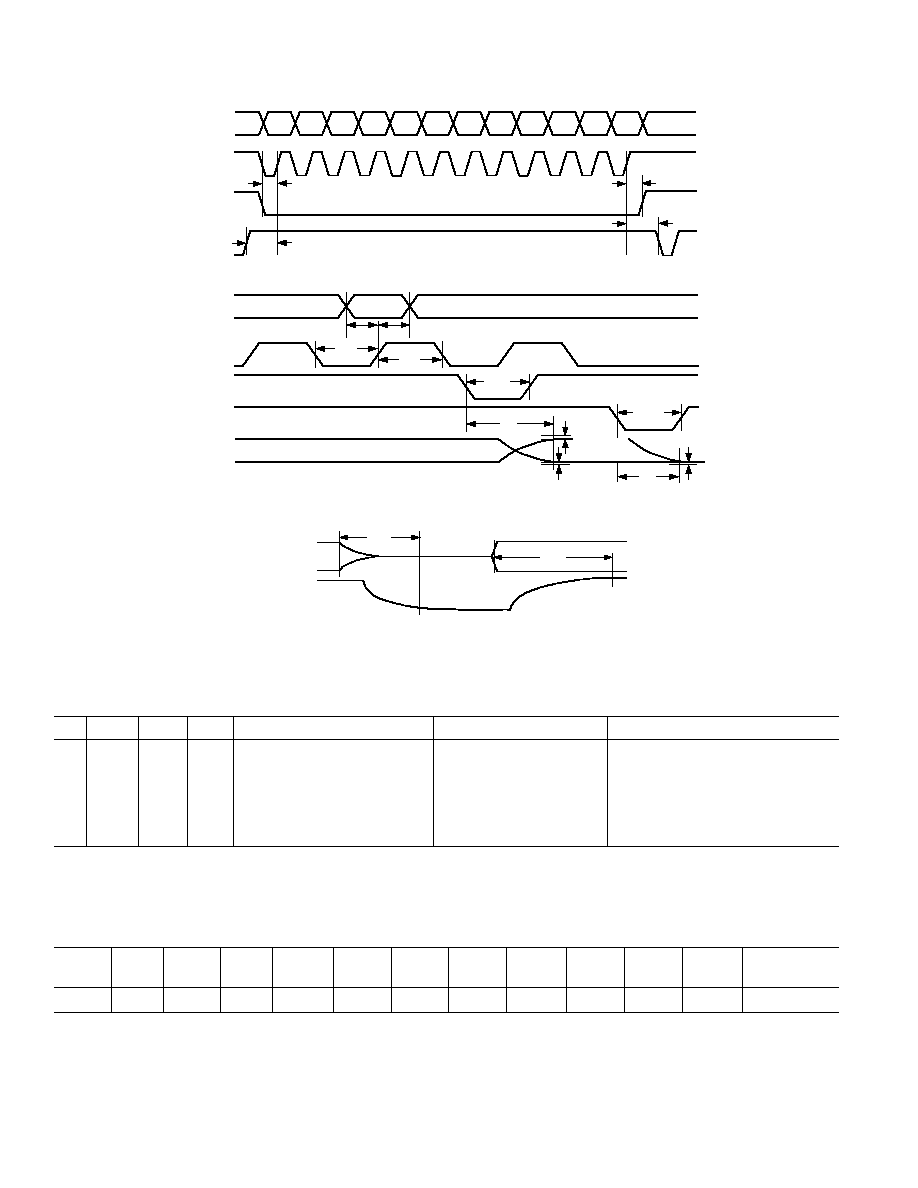
SDI
CLK
CS
LDAC
SA
SI
A1
A0
D7
D6
D5
D4
D3
D2
D1
D0
t
CSH
t
LD2
t
CSS
t
LD1
SDI
CLK
CLR
LDAC
FS
ZS
V
OUT
t
DS
t
DH
t
CL
t
CH
t
LDW
t
S
t
CLRW
t
S
1 LSB
ERROR BAND
Figure 2. AD7304 Timing Diagram
t
SDR
SDI/SHDN
I
DD
t
SDN
Figure 3. AD7304 Timing Diagram
Table I. AD7304 Control Logic Truth Table
CS
CLK
LDAC CLR
Serial Shift Register Function
Input REG Function
DAC Register Function
H
X
H
H
No Effect
No Effect
No Effect
L
+
H
H
Data Advanced 1 Bit
No Effect
No Effect
+
L
H
H
No Effect
Updated with SR Contents
2
No Effect
H
X
L
H
No Effect
Latched with SR Contents
2
All Input Register Contents Transferred
3
H
X
H
≠
No Effect
Loaded with 00
H
Loaded with 00
H
H
X
H
+
No Effect
Latched with 00
H
Latched with 00
H
NOTES
1
+ positive logic transition; ≠ negative logic transition; X Don't Care.
2
One Input Register receives the data bits D7≠D0 decoded from the SR address bits (A1, A0); where REG A = (0, 0); B = (0, 1); C = (1, 0); D = (1, 1).
3
LDAC is a level-sensitive input.
Table II. AD7304 Serial Input Register Data Format, Data Is Loaded in the MSB-First Format
MSB
LSB
B11
B10
B9
B8
B7
B6
B5
B4
B3
B2
B1
B0
AD7304 SAC
SDC
A1
A0
D7
D6
D5
D4
D3
D2
D1
D0
If B11 (SAC), Shutdown All Channels, is set to logic LOW, all DACs are placed in a power shutdown mode, all output voltages become high resistance. If B10 (SDC),
Shutdown Decoded Channel, is set to logic LOW, only the DAC decoded by address bits A1 and A0 is placed in the shutdown mode.
≠5≠
AD7304/AD7305
REV. A
Table III. AD7305 Control Logic Truth Table
WR
A1
A0
LDAC Input Register Function
DAC Register Function
L
L
L
H
REG A Loaded with DB0≠DB7
Latched with Previous Contents, No Change
+
L
L
H
REG A Latched with DB0≠DB7
Latched with Previous Contents, No Change
L
L
H
H
REG B Loaded with DB0≠DB7
Latched with Previous Contents, No Change
+
L
H
H
REG B Latched with DB0≠DB7
Latched with Previous Contents, No Change
L
H
L
H
REG C Loaded with DB0≠DB7
Latched with Previous Contents, No Change
+
H
L
H
REG C Latched with DB0≠DB7
Latched with Previous Contents, No Change
L
H
H
H
REG D Loaded with DB0≠DB7
Latched with Previous Contents, No Change
+
H
H
H
REG D Latched with DB0≠DB7
Latched with Previous Contents, No Change
H
X
X
L
No Effect
All Input Register Contents Loaded, Register Transparent
L
X
X
L
Input REG x Transparent to DB0≠DB7
Register Transparent
H
X
X
+
No Effect
All Input Register Contents Latched
H
X
X
H
No Effect, Device Not Selected
No Effect, Device Not Selected
NOTES
1
+ positive logic transition; ≠ negative logic transition; X Don't Care.
2
LDAC is a level sensitive input.
PIN CONFIGURATIONS
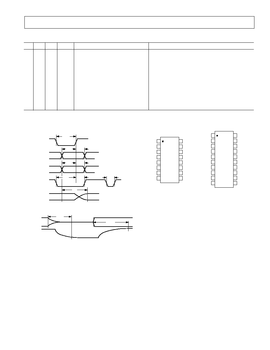
TOP VIEW
(Not to Scale)
16
15
14
13
12
11
10
9
1
2
3
4
5
6
7
8
V
OUT
B
V
OUT
A
V
SS
V
REF
B
V
REF
A
GND
LDAC
CLR
V
OUT
C
V
OUT
D
V
DD
V
REF
C
V
REF
D
SDI/SHDN
CLK
CS
AD7304
TOP VIEW
(Not to Scale)
20
19
18
17
16
15
14
13
12
11
1
2
3
4
5
6
7
8
9
10
AD7305
DB5
DB6
V
OUT
A
V
SS
V
REF
DB7
LDAC
GND
DB2
DB1
V
OUT
D
V
DD
A0/SHDN
DB0
WR
A1
V
OUT
B
V
OUT
C
DB4
DB3
t
AH
t
DH
t
LH
t
LDW
t
WR
t
AS
t
DS
t
LS
t
S
1 LSB
ERROR BAND
A0, A1
WR
D0≠D7
LDAC
V
OUT
Figure 4. AD7305 Timing Diagram
t
SDR
A0/SHDN
I
DD
t
SDN
Figure 5. AD7305 Timing Diagram

AD7304/AD7305
≠6≠
REV. A
AD7304 PIN FUNCTION DESCRIPTIONS
Pin #
Name
Function
1
V
OUT
B
Channel B rail-to-rail buffered DAC voltage output. Full scale set by reference voltage applied to V
REF
B pin. Output
is open circuit when SHDN is enabled.
2
V
OUT
A
Channel A rail-to-rail buffered DAC voltage output. Full scale set by reference voltage applied to V
REF
A pin. Output
is open circuit when SHDN is enabled.
3
V
SS
Negative Power Supply Input. Specified range of operation 0 V to ≠5.5 V.
4
V
REF
A
Channel A Reference Input. Establishes V
OUT
A full-scale voltage. Specified range of operation V
SS
< V
REF
A < V
DD
.
5
V
REF
B
Channel B Reference Input. Establishes V
OUT
B full-scale voltage. Specified range of operation V
SS
< V
REF
B < V
DD
.
6
GND
Common Analog and Digital Ground.
7
LDAC
Load DAC register strobe, active low. Transfers all four Input Register data into their DAC registers. Asynchronous
active low input. DAC Register is transparent when LDAC = 0. See Control Logic Truth Table for operation.
8
CLR
Clears all Input and DAC registers to the zero condition. Asynchronous active low input. The serial register is not effected .
9
CS
Chip Select, Active Low Input. Disables shift register loading when high. Transfers Serial Input Register Data to the
decoded Input Register when CS returns HIGH. Does not effect LDAC operation.
10
CLK
Clock input, positive edge clocks data into shift register. Disabled by chip select CS.
11
SDI/SHDN
Serial Data-Input loads directly into the shift register, MSB first. Hardware shutdown (SHDN) control input, active
when pin is left floating by a three-state logic driver. Does not effect DAC register contents as long as power is
present on V
DD
.
12
V
REF
D
Channel D Reference Input. Establishes V
OUT
D full-scale voltage. Specified range of operation V
SS
< V
REF
D < V
DD
.
13
V
REF
C
Channel C Reference Input. Establishes V
OUT
C full-scale voltage. Specified range of operation V
SS
< V
REF
C < V
DD
.
14
V
DD
Positive power supply input. Specified range of operation +2.7 V to +5.5 V.
15
V
OUT
D
Channel D rail-to-rail buffered DAC voltage output. Full-scale set by reference voltage applied to V
REF
D pin. Output
is open circuit when SHDN is enabled.
16
V
OUT
C
Channel C rail-to-rail buffered DAC voltage output. Full-scale set by reference voltage applied to V
REF
C pin. Output
is open circuit when SHDN is enabled.
AD7305 PIN FUNCTION DESCRIPTIONS
Pin #
Name
Function
1
V
OUT
B
Channel B rail-to-rail buffered DAC voltage output. Full scale set by reference voltage applied to V
REF
B pin. Output
is open circuit when SHDN is enabled.
2
V
OUT
A
Channel A rail-to-rail buffered DAC voltage output. Full scale set by reference voltage applied to V
REF
A pin. Output
is open circuit when SHDN is enabled.
3
V
SS
Negative Power Supply Input. Specified range of operation 0 V to ≠5.5 V.
4
V
REF
Channel B Reference Input. Establishes V
OUT
full-scale voltage. Specified range of operation V
SS
< V
REF
< V
DD
.
5
GND
Common Analog and Digital Ground.
6
LDAC
Load DAC register strobe, active low. Transfers all four Input Register data into their DAC registers. Asynchronous
active low input. DAC Register is transparent when LDAC = 0. See Control Logic Truth Table for operation.
7
DB7
MSB Digital Input Data Bit.
8
DB6
Data Bit 6.
9
DB5
Data Bit 5.
10
DB4
Data Bit 4.
11
DB3
Data Bit 3.
12
DB2
Data Bit 2.
13
DB1
Data Bit 1.
14
DB0
LSB Digital Input Data Bit.
15
WR
Write data into Input Register control line, active low. See Control Logic Truth Table for operation.
16
A1
Address Bit 1.
17
A0/SHDN
Address Bit 0/Hardware shutdown (SHDN) control input, active when pin is left floating by a three-state logic driver.
Does not effect DAC register contents as long as power is present on V
DD
.
18
V
DD
Positive Power Supply Input. Specified range of operation +2.7 V to +5.5 V.
19
V
OUT
D
Channel D rail-to-rail buffered DAC voltage output. Full scale set by reference voltage applied to V
REF
D pin. Output
is open circuit when SHDN is enabled.
20
V
OUT
C
Channel C rail-to-rail buffered DAC voltage output. Full scale set by reference voltage applied to V
REF
C pin. Output
is open circuit when SHDN is enabled.
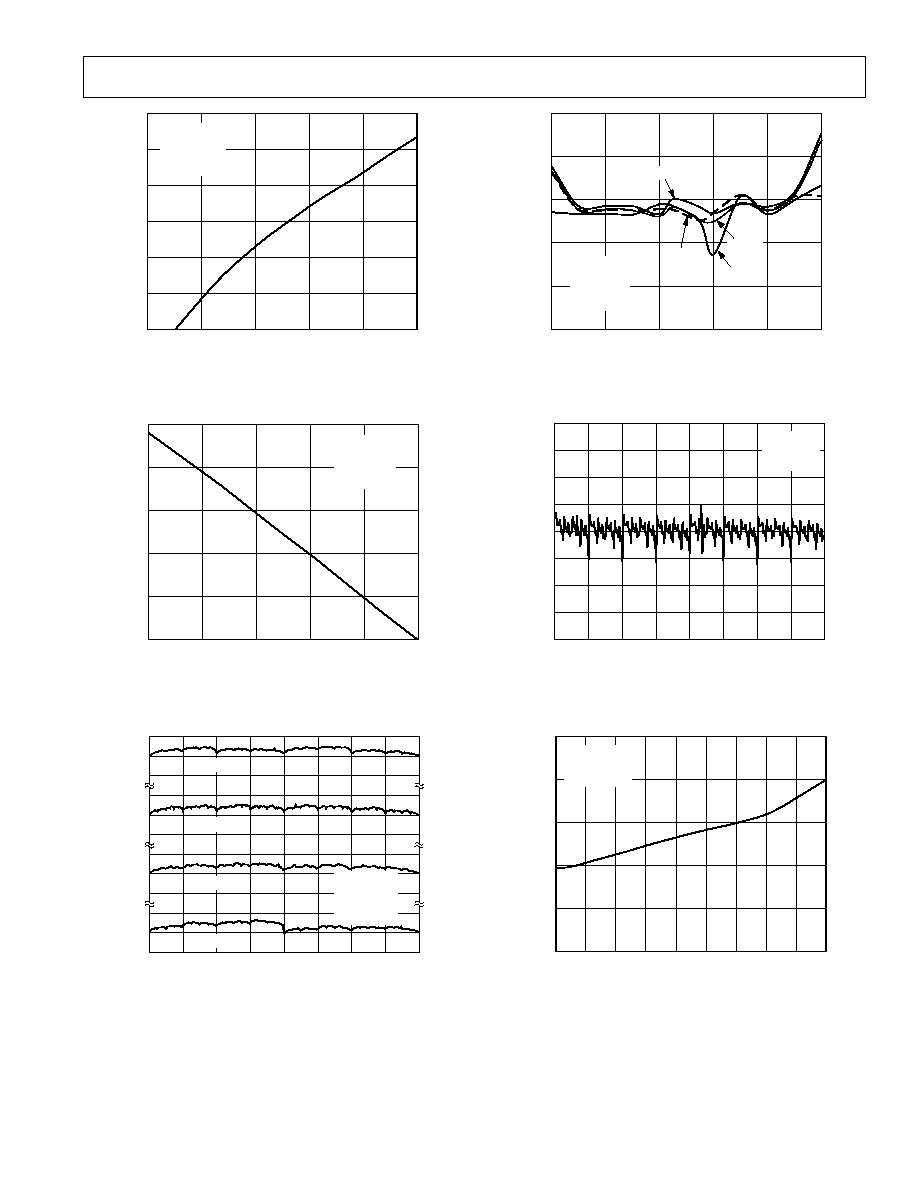
V
OUT
≠ mV
144
120
0
0
15
3
I
OUT
SINK CURRENT
≠
mA
6
9
12
96
72
48
24
V
DD
= +5V
V
SS
= ≠5V
V
REF
= V
DD
DATA = 00
H
Figure 6. I
OUT
SINK vs. V
OUT
Rail-to-Rail Performance
V
OUT
OUTPUT VOLTAGE ≠ Volts
≠35
≠28
0
4.0
5.0
4.2
I
OUT
SOURCE CURRENT
≠
mA
4.4
4.6
4.8
≠21
≠14
≠7
V
DD
= +5V
V
SS
= ≠5V
V
REF
= V
DD
DATA = FF
H
Figure 7. I
OUT
SOURCE vs. V
OUT
Rail-to-Rail Performance
CODE ≠ Decimal
1
0
0
256
32
INL
≠
LSB
64
96
128
160
192
224
0
0
1
≠1
1
≠1
1
≠1
0
≠1
DAC A
DAC B
DAC C
DAC D
V
DD
= +5V
V
SS
= ≠5V
V
REF
= +2.5V
T
A
= +25 C
Figure 8. INL vs. Code, All DAC Channels
REFERENCE INPUT VOLTAGE ≠ Volts
1.0
0.6
≠1.0
≠5.0
5.0
≠3.0
INL
≠
LSB
≠1.0
1.0
3.0
0.2
≠0.2
≠0.6
DATA = 80
H
V
DD
= +5V
V
SS
= ≠5V
T
A
= +25 C
DAC A
DAC B
DAC C
DAC D
Figure 9. INL vs. Reference Input Voltage
CODE ≠ Decimal
0.500
≠0.500
0
256
32
DNL
≠
LSB
64
96
128
160
192
224
0.375
0.000
≠0.125
≠0.250
≠0.375
0.250
0.125
V
DD
= +5V
V
SS
= ≠5V
V
REF
= 2.5V
Figure 10. DNL vs. Code
TEMPERATURE ≠ C
4.0
3.6
2.0
≠55
125
≠35
ZERO SCALE VOLTAGE
≠
mV
≠15
5
25
45
65
85
105
3.2
2.8
2.4
V
DD
= +5.5V
V
SS
= 0V
V
REF
= +5.45V
Figure 11. Zero Scale Voltage vs. Temperature
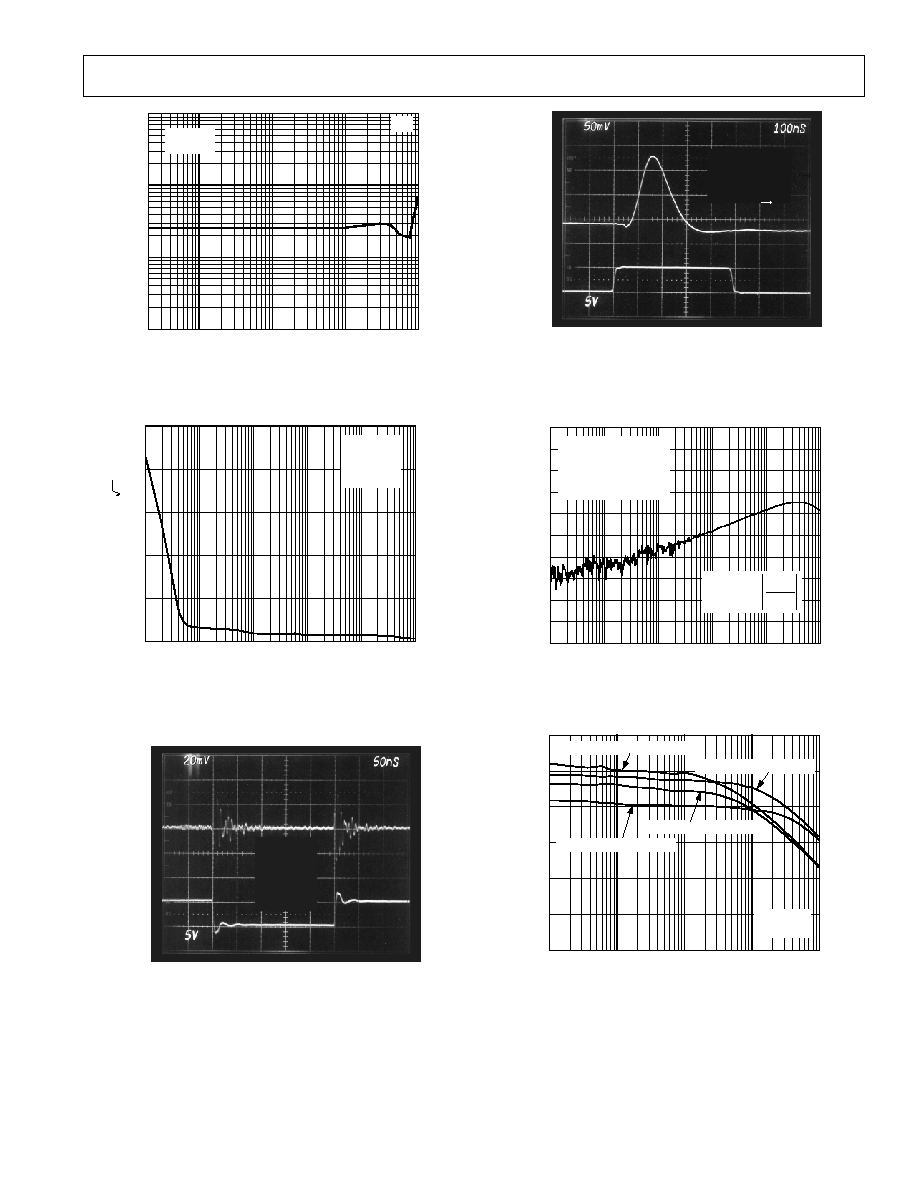
≠7≠
Typical Performance Characteristics≠AD7304/AD7305
REV. A

AD7304/AD7305
≠8≠
REV. A
V
OUT
CS
5V
0V
0V
V
DD
= +5V
V
REF
= +4V
DATA = 00
H
FF
H
2 s/DIV
Figure 12. Large-Signal Settling Time
V
OUTA
≠5V
0V
5V
≠5V
0V
5V
V
REFIN
( 5V @
50kHz)
DATA = FF
H
2 s/DIV
Figure 13. Multiplying Mode Step Response and Output
Slew Rate
FREQUENCY ≠ Hz
6
≠8
10k
10M
GAIN
≠
dB
4
1M
100k
0
≠4
≠6
V
DD
= +5V
V
SS
= ≠5V
DATA = FF
H
V
REF
= 100mV rms
f
≠3dB
= 2.6MHz
Figure 14. Multiplying Mode Gain vs. Frequency
V
OUT
CS
R
L
= 10k
R
L
= 70k
NO LOAD
V
DD
= +5V
C
L
= 150pF
5 s/DIV
Figure 15. Time to Shutdown
V
OUT
CS
I
DD
1mA/V
V
DD
= +5V
Figure 16. Shutdown Recovery Time (Wakeup)
V
REF
AMPLITUDE ≠ V p-p
10
1
0.001
10m
10
1
THD
≠
%
2
3
4
5
6
7
8
9
0.1
0.010
V
DD
= +5V
V
SS
= ≠5V
A
Figure 17. THD vs. Reference Input Amplitude
≠9≠
AD7304/AD7305
REV. A
FREQUENCY ≠ Hz
1
0.1
0.001
20
100k
100
THD
≠
%
1k
10k
0.010
A
V
DD
= +5V
V
SS
= ≠5V
Figure 18. THD vs. Frequency
FREQUENCY ≠ Hz
3.0
2.4
0
1
100k
10
NOISE DENSITY
≠
V/ Hz
100
1k
10k
1.8
1.2
0.6
V
DD
= +5V
V
SS
= ≠5V
V
REF
= 4V
DATA = FF
H
Figure 19. Output Noise Voltage Density vs. Frequency
V
OUTB
50ns/DIV
CLK
V
DD
= +5V
V
SS
= ≠5V
V
REF
= 2.5V
DAC A = FF
H
DAC B = OO
H
F = 2MHz
Figure 20. Digital Feedthrough
V
OUT
CS
V
DD
= +5V
V
SS
= ≠5V
V
REF
= 2.5V
F = 1MHz
DATA = 80
H
7F
H
Figure 21. Midscale Transition Glitch
FREQUENCY ≠ Hz
40
20
≠160
100
10M
1k
CROSS TALK
≠
dB
10k
1M
0
≠20
≠40
V
DD
= +5V
V
SS
= ≠5V
V
REF
= 50mV rms
DAC A DATA = FF
H
DAC B, C, D DATA = 00
H
≠60
≠80
≠100
≠120
≠140
V
OUTB
V
REF
CT = 20 LOG
100k
Figure 22. Crosstalk vs. Frequency
FREQUENCY ≠ Hz
60
0
10
100
PSRR
≠
dB
1k
100k
50
40
30
20
10
10k
DATA = 80
H
T
A
= +25 C
+PSRR, V
DD
= +5V 10%
≠PSRR, V
SS
= ≠5V 10%
+PSRR, V
DD
= +3V 10%
≠PSRR, V
SS
= ≠3V 10%
Figure 23. Power Supply Rejection vs. Frequency

AD7304/AD7305
≠10≠
REV. A
DIGITAL INPUT VOLTAGE ≠ Volts
12
10
0
0
5
1
SUPPLY CURRENT
≠
mA
2
3
4
8
6
4
2
V
DD
= +5V
V
SS
= ≠5V
V
REF
= 2.5V
A0 = 5V
ALL OTHER DIGITAL
PINS VARYING
I
DD
I
SS
Figure 24. Supply Current vs. Digital Input Voltage
DIGITAL INPUT VOLTAGE ≠ Volts
10.0000
1.0000
0.0001
0
5
1
SUPPLY CURRENT
≠
mA
2
3
4
0.1000
0.0100
0.0010
V
DD
= +5V
V
SS
= ≠5V
V
REF
= 2.5V
ALL DIGITAL PINS VARY,
EXCEPT A0 = 5V
I
DD
I
SS
Figure 25. Shutdown Supply Current vs. Digital Input
Voltage (A0 Only)
TEMPERATURE ≠ C
5.0
4.4
2.0
≠55
125
≠35
SUPPLY CURRENT
≠
mA
≠15
5
25
45
65
85
105
3.8
3.2
2.6
V
DD
= +5V
V
SS
= ≠5V
V
REF
= 2.5V
I
DD
AND I
SS
Figure 26. Supply Current vs. Temperature
TEMPERATURE ≠ C
80
20
≠55
125
≠35
SHUTDOWN SUPPLY
≠
A
≠15
5
25
45
65
85
105
70
60
50
40
30
V
DD
= +5.5V
V
SS
= ≠5.5V
V
REF
= 2.5V
PIN A0 FLOATING
Figure 27. Shutdown Supply Current vs. Temperature
DEGREES CELCIUS
0.08
≠0.04
0
84
NORMALIZED TOTAL UNADJUSTED
ERROR DRIFT
≠
LSB
168
252
336
420
504
0.04
0
≠0.08
READING MADE AT T
A
= +25 C
SAMPLE SIZE = 924 UNITS
V
DD
= 2.7V
V
DD
= 5.5V
Figure 28. Normalized TUE Drift Accelerated by Burn-In
Hours of Operation @ 150
∞C
≠11≠
AD7304/AD7305
REV. A
CIRCUIT OPERATION
The AD7304/AD7305 are a set of four-channel, 8-bit, voltage-
output, digital-to-analog converters differing primarily in digital
logic interface and number of reference inputs. Both parts share
the same internal DAC design and true rail-to-rail output buff-
ers. The AD7304 contains four independent multiplying refer-
ence inputs, while the AD7305 has one common reference input.
The AD7304 uses a 3-wire SPI compatible serial data interface,
while the AD7305 offers a 8-bit parallel data interface.
D/A Converter Section
Each part contains four voltage-switched R-2R ladder DACs.
Figure A shows a typical equivalent DAC. These DACs are
designed to operate both single-supply or dual supply, depend-
ing on whether the user supplies a negative voltage on the V
SS
pin. In a single-supply application the V
SS
is tied to ground. In
either mode the DAC output voltage is determined by the V
REF
input voltage and the digital data (D) loaded into the corre-
sponding DAC register according to Equation 1.
V
OUT
= V
REF
◊ D/256
(1)
Note that the output full-scale polarity is the same as the V
REF
polarity for dc reference voltages.
V
REF
DB7
2R
V
DD
V
SS
V
OUT
R
2R
DB6
2R
DB0
2R
Figure 29. Typical Equivalent DAC Channel
These DACs are also designed to accommodate ac reference
input signals. As long as the ac signals are maintained between
V
SS
< V
REF
<V
DD
, the user can expect 50 kHz of full-power
multiplying bandwidth performance. In order to use negative
input reference voltages, the V
SS
pin must be biased with a nega-
tive voltage of equal or greater magnitude than the reference
voltage.
The reference inputs are code-dependent, exhibiting worst case
minimum resistance values specified in the parametric specifica-
tion table. The DAC outputs V
OUT
A, B, C, D are each capable
of driving 2 k
loads in parallel with up to 500 pF loads. Output
source and sink current is shown in Figures 6 and 7. The output
slew rate is nominally 3.6 V/
µs while operating from ±5 V sup-
plies. The low output impedance of the buffers minimizes
crosstalk between analog input channels. At 100 kHz, 65 dB of
channel-to-channel isolation exists (Figure 22). Output voltage
noise is plotted in Figure 19. In order to maintain good analog
performance, power supply bypassing of 0.01
µF in parallel with
1
µF is recommended. The true rail-to-rail capability of the
AD7304/AD7305 allows the user to connect the reference inputs
directly to the same supply as the V
DD
or V
SS
pin (Figure 30).
Under these conditions clean power supply voltages (low ripple,
avoid switching supplies) appropriate for the application should
be used.
V
DD
V
SS
V
OUT
X
120k
Q1
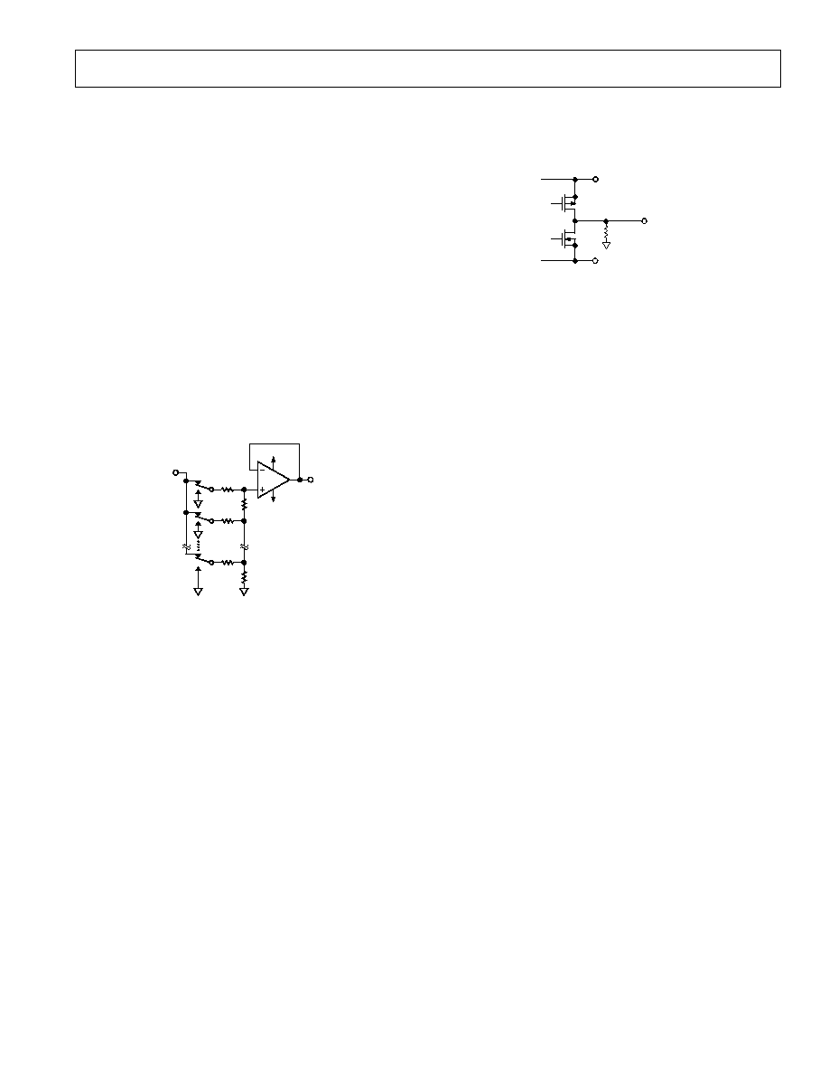
Q2
Figure 30. Equivalent DAC Amplifier Output Circuit
AD7304 SERIAL DATA INTERFACE
The AD7304 uses a 3-wire (CS, SDI, CLK) SPI compatible
serial data interface. New serial data is clocked into the serial
input register in a 12-bit data-word format. MSB bits are loaded
first. Table II defines the 12 data-word bits. Data is placed on
the SDI/SHDN pin and clocked into the register on the positive
clock edge of CLK subject to the data setup and data hold time
requirements specified in the TIMING SPECIFICATIONS.
Data can only be clocked in while the CS chip select pin is
active low. Only the last 12-bits clocked into the serial register
will be interrogated when the CS pin returns to the logic high
state, extra data bits are ignored. Since most microcontrollers
output serial data in 8-bit bytes, two right justified data bytes
can be written to the AD7304. Keeping the CS line low between
the first and second byte transfer will result in a successful serial
register update.
Once the data is properly aligned in the shift register the positive
edge of the CS initiates either the transfer of new data to the
target DAC register, determined by the decoding of address bits
A1 and A0, or the shutdown features will be activated based on
the SAC or SDC bits. When either SAC or SDC pins are set
(Logic = 0) the loading of new data determined by Bits B9 to
B0 are still loaded, but the results do not appear on the buffer
outputs until the device is brought out of the shutdown state.
The selected DAC output voltages become high impedance with
a nominal resistance of 120 k
to ground, Figure 30. If both
SAC and SDC pins are set, all channels are still placed in the
shutdown mode. When the AD7304 has been programmed into
the power shutdown state, the present DAC register data is
maintained as long as V
DD
remains greater than 2.7 volts. The
remaining characteristics of the software serial interface are
defined by Tables I, II and Figure 3 timing diagram.
Two additional pins CLR and LDAC on the AD7304 provide
hardware control over the clear function and the DAC Register
loading. If these functions are not needed the CLR pin can be
tied to logic high, and the LDAC pin can be tied to logic low.
The asynchronous input CLR pin forces all input and DAC
registers to the zero-code state. The asynchronous LDAC pin
can be strobed to active low when all DAC Registers need to be
updated simultaneously from their respective Input Registers.
The LDAC pin places the DAC Register in a transparent mode
while in the logic low state.

AD7304/AD7305
≠12≠
REV. A
AD7304
INPUT
REGISTER
R
DAC A
OE
DAC A
REGISTER
R
INPUT
REGISTER
R
DAC B
OE
DAC C
REGISTER
R
DAC B
REGISTER
R
INPUT
REGISTER
R
DAC C
OE
DAC D
REGISTER
R
DACA
B
C
D
2:4
DECODE
A0
A1
SDC
SAC
D0
D1
D2
D3
D4
D5
D6
D7
8
EN
320k
280k
80k
640k
680k
V
DD
LDAC
V
SS
V
OUT
C
CS
SDI
V
OUT
B
V
OUT
A
V
DD
D Q
g
D Q
g
D Q
g
D Q
g
INPUT
REGISTER
R
POWER-
ON
RESET
V
REF
A
V
REF
B
V
REF
C
V
REF
D
V
OUT
D
CLR
GND
CLK
DAC D
OE
Figure 31. AD7304 Equivalent Logic Interface
AD7304 Hardware Shutdown SHDN
If a three-state driver is used on the SDI/SHDN pin, the AD7304
can be placed into a power shutdown mode when the SDI/
SHDN pin is placed in a high impedance state. For proper
operation no other termination voltages should be present on
this pin. An internal window comparator will detect when the
logic voltage on the SHDN pin is between 28% and 36% of
V
DD
. A high impedance internal bias generator provides this
voltage on the SHDN pin. The four DAC output voltages be-
come high impedance with a nominal resistance of 120 k
to
ground. See Figure 30 for an equivalent circuit.
AD7304/AD7305 POWER ON RESET
When the V
DD
power supply is turned on, an internal reset
strobe forces all the Input and DAC registers to the zero-code
state. The V
DD
power supply should have a monotonically in-
creasing ramp in order to have consistent results, especially in
the region of V
DD
= 1.5 V to 2.3 V. The V
SS
supply has no effect
on the power ON reset performance. The DAC register data
will stay at zero until a valid serial register software load takes
place. In the case of the double buffered AD7305 the output
DAC register can only be changed once the LDAC strobe is
initiated.
AD7305 PARALLEL DATA INTERFACE
The AD7305 has an 8-bit parallel interface DB7 = MSB,
DB0 = LSB. Two address Bits A1 and A0 are decoded when an
active low write strobe is placed on the WR pin, see Table III.
The WR is a level-sensitive input pin, therefore the data setup
and data hold times defined in the TIMING SPECIFICATIONS
need to be adhered to.
The LDAC pin provides the capability of simultaneously updat-
ing all DAC registers with new data from the Input Registers at
the same time. This will result in the analog outputs all chang-
ing to their new values at the same time. The LDAC pin is a
level-sensitive input. If the simultaneous update feature is not
required the LDAC pin can be tied to logic low. When the
LDAC is tied to logic low, the DAC Registers become transpar-
ent and the Input Register data determines the DAC output
voltage. See Figure 32 for an equivalent interface logic diagram.
AD7226 Pin Compatibility
By tying the LDAC pin to ground, the AD7305 has the same
pin out and functionality as the AD7226, with the exception of
a lower power supply operating voltage.
AD7305 Hardware Shutdown SHDN
If a three state driver is used on the A0/SHDN pin, the AD7305
can be placed into a power shutdown mode when the A0/SHDN
pin is placed in a high impedance state. For proper operation no
other termination voltages should be present on this pin. An
internal window comparator will detect when the logic voltage
on the SHDN pin is between 28% and 36% of V
DD
. A high
impedance internal bias generator provides this voltage on the
SHDN pin. The four DAC output voltages become high imped-
ance with a nominal resistance of 120 k
to ground.
ESD Protection Circuits
All logic input pins contain back-biased ESD protection Zeners
connected to ground (GND). The V
REF
pins also contain a
back-biased ESD protection Zener connected to V
DD
(see
Figure 33).
GND
DIGITAL
INPUTS
V
DD
V
REF
X
Figure 33. Equivalent ESD Protection Circuits
AD7305
INPUT
REGISTER
R
DAC A
OE
DAC A
REGISTER
R
INPUT
REGISTER
R
DAC B
OE
DAC C
REGISTER
R
DAC B
REGISTER
R
INPUT
REGISTER
R
DAC C
OE
DAC D
REGISTER
R
DAC A
B
C
D
2:4
DECODE
8
320k
280k
80k
640k
680k
V
DD
LDAC
V
SS
V
OUT
C
WR
V
OUT
B
V
OUT
A
V
DD
INPUT
REGISTER
R
POWER-
ON
RESET
V
REF
V
OUT
D
GND
DATA
DB0≠DB7
DAC D
OE
A1
A0/SHDN
Figure 32. AD7305 Equivalent Logic Interface

≠13≠
AD7304/AD7305
REV. A
APPLICATIONS
The AD7304/AD7305 is inherently a 2-quadrant multiplying
D/A converter. That is, it can easily be set up for unipolar out-
put operation. The full-scale output polarity is the same as the
reference input voltage polarity.
In some applications it may be necessary to generate the full
4-quadrant multiplying capability or a bipolar output swing.
This is easily accomplished using an external true rail-to-rail op
amp, such as the OP295. Connecting the external amplifier with
two equal value resistors as shown in Figure 34 results in a full
4-quadrant multiplying circuit. In this circuit the amplifier pro-
vides a gain of two, which increases the output span magnitude
to 10 volts. The transfer equation of this circuit shows that both
negative and positive output voltages are created as the input
data (D) is incremented from code zero (V
OUT
= ≠5 V) to mid-
scale (V
OUT
= 0 V) to full scale (V
OUT
= +5 V).
V
OUT
= (D/128 ≠1)
◊ V
REF
(2)
+5V
10k
10k
AD7304
REF
≠5V < V
OUT
< +5V
Figure 34. Four-Quadrant Multiplying Application Circuit

AD7304/AD7305
≠14≠
REV. A
16-Lead Wide SOIC
(R-16)
0.2992 (7.60)
0.2914 (7.40)
16
9
8
1
0.4133 (10.50)
0.3977 (10.00)
0.4193 (10.65)
0.3937 (10.00)
PIN 1
SEATING
PLANE
0.0118 (0.30)
0.0040 (0.10)
0.0192 (0.49)
0.0138 (0.35)
0.1043 (2.65)
0.0926 (2.35)
0.0500
(1.27)
BSC
0.0125 (0.32)
0.0091 (0.23)
0.0500 (1.27)
0.0157 (0.40)
0.0291 (0.74)
0.0098 (0.25)
x 45
8
0
16-Lead Plastic DIP
(N-16)
16
1
8
9
0.840 (21.33)
0.745 (18.93)
0.280 (7.11)
0.240 (6.10)
PIN 1
SEATING
PLANE
0.022 (0.558)
0.014 (0.356)
0.060 (1.52)
0.015 (0.38)
0.210 (5.33)
MAX
0.130
(3.30)
MIN
0.070 (1.77)
0.045 (1.15)
0.100
(2.54)
BSC
0.160 (4.06)
0.115 (2.93)
0.325 (8.25)
0.300 (7.62)
0.015 (0.381)
0.008 (0.204)
0.195 (4.95)
0.115 (2.93)
16-Lead TSSOP
(RU-16)
16
9
8
1
0.201 (5.10)
0.193 (4.90)
0.256 (6.50)
0.246 (6.25)
0.177 (4.50)
0.169 (4.30)
PIN 1
SEATING
PLANE
0.006 (0.15)
0.002 (0.05)
0.0118 (0.30)
0.0075 (0.19)
0.0256
(0.65)
BSC
0.0433
(1.10)
MAX
0.0079 (0.20)
0.0035 (0.090)
0.028 (0.70)
0.020 (0.50)
8
0
20-Lead SOIC
(R-20)
SEATING
PLANE
0.0118 (0.30)
0.0040 (0.10)
0.0192 (0.49)
0.0138 (0.35)
0.1043 (2.65)
0.0926 (2.35)
0.0500
(1.27)
BSC
0.0125 (0.32)
0.0091 (0.23)
0.0500 (1.27)
0.0157 (0.40)
0.0291 (0.74)
0.0098 (0.25)
x 45
8
0
20
11
10
1
0.5118 (13.00)
0.4961 (12.60)
0.4193 (10.65)
0.3937 (10.00)
0.2992 (7.60)
0.2914 (7.40)
PIN 1
20-Lead Plastic DIP
(N-20)
20
1
10
11
1.060 (26.90)
0.925 (23.50)
0.280 (7.11)
0.240 (6.10)
PIN 1
SEATING
PLANE
0.022 (0.558)
0.014 (0.356)
0.210 (5.33)
MAX
0.130
(3.30)
MIN
0.070 (1.77)
0.045 (1.15)
0.100
(2.54)
BSC
0.160 (4.06)
0.115 (2.93)
0.060 (1.52)
0.015 (0.38)
0.325 (8.25)
0.300 (7.62)
0.015 (0.381)
0.008 (0.204)
0.195 (4.95)
0.115 (2.93)
20-Lead Thin Surface Mount (TSSOP)
(RU-20)
20
11
10
1
0.260 (6.60)
0.252 (6.40)
0.256 (6.50)
0.246 (6.25)
0.177 (4.50)
0.169 (4.30)
PIN 1
SEATING
PLANE
0.006 (0.15)
0.002 (0.05)
0.0118 (0.30)
0.0075 (0.19)
0.0256 (0.65)
BSC
0.0433
(1.10)
MAX
0.0079 (0.20)
0.0035 (0.090)
0.028 (0.70)
0.020 (0.50)
8
0
OUTLINE DIMENSIONS
Dimensions shown in inches and (mm).
C3252a-2
≠
2/98
PRINTED IN U.S.A.