 | ÐлекÑÑоннÑй компоненÑ: AD7392 | СкаÑаÑÑ:  PDF PDF  ZIP ZIP |
Äîêóìåíòàöèÿ è îïèñàíèÿ www.docs.chipfind.ru
REV. A
Information furnished by Analog Devices is believed to be accurate and
reliable. However, no responsibility is assumed by Analog Devices for its
use, nor for any infringements of patents or other rights of third parties
which may result from its use. No license is granted by implication or
otherwise under any patent or patent rights of Analog Devices.
a
AD7392/AD7393
One Technology Way, P.O. Box 9106, Norwood, MA 02062-9106, U.S.A.
Tel: 781/329-4700
World Wide Web Site: http://www.analog.com
Fax: 781/326-8703
© Analog Devices, Inc., 1999
+3 V, Parallel Input
Micropower 10- and 12-Bit DACs
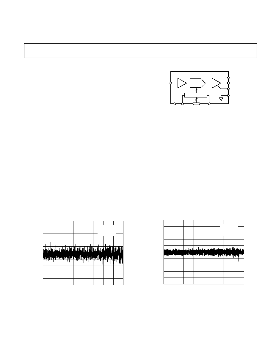
FUNCTIONAL BLOCK DIAGRAM
12
12
12-BIT
DAC
DAC REGISTER
V
REF
SHDN
AGND
RS
DB0DB11
CS
DGND
AD7392
V
DD
V
OUT
FEATURES
Micropower: 100 A
0.1 A Typical Power Shutdown
Single-Supply +2.7 V to +5.5 V Operation
Compact 1.1 mm Height TSSOP-20 Package
AD7392/12-Bit Resolution
AD7393/10-Bit Resolution
0.9 LSB Differential Nonlinearity Error
APPLICATIONS
Automotive 0.5 V to 4.5 V Output Span Voltage
Portable Communications
Digitally Controlled Calibration
PC Peripherals
GENERAL DESCRIPTION
The AD7392/AD7393 family of 10- and 12-bit voltage-output
digital-to-analog converters is designed to operate from a single
+3 V supply. Built using a CBCMOS process, these monolithic
DACs offer the user low cost and ease of use in single-supply
+3 V systems. Operation is guaranteed over the supply voltage
range of +2.7 V to +5.5 V, making this device ideal for battery
operated applications.
The full-scale voltage output is determined by the external
reference input voltage applied. The rail-to-rail REF
IN
to
DAC
OUT
allows for a full-scale voltage set equal to the positive
supply V
DD
or any value in between. The voltage outputs are
capable of sourcing 5 mA.
A 12-bit wide data latch loads with a 45 ns write time allowing
interface to the fastest processors without wait states.
Additionally, an asynchronous
RS input sets the output to zero
scale at power on or upon user demand.
Both parts are offered in the same pinout to allow users to select
the amount of resolution appropriate for their applications
without circuit card changes.
The AD7392/AD7393 are specified for operation over the ex-
tended industrial (40
°
C to +85
°
C) temperature range. The
AD7393AR is specified for the 40
°
C to +125
°
C automotive
temperature range. AD7392/AD7393s are available in plastic
DIP, and 20-lead SOIC packages. The AD7393ARU is avail-
able for ultracompact applications in a thin 1.1 mm height
TSSOP-20 package.
For serial data input, 8-lead packaged versions, see the AD7390
and AD7391 products.
CODE Decimal
1
1
0.4
0.2
0.4
0.6
0.8
0.2
0
0.8
0.6
0
4096
512
DNL LSB
1024
1536
2048
2560
3072
3584
AD7392
V
DD
= +2.7V
V
REF
= +2.5V
T
A
= 25 C
Figure 1. AD7392 Differential Nonlinearity Error vs. Code
CODE Decimal
1024
128
256
384
512
640
768
896
0
AD7393
V
DD
= +2.7V
V
REF
= +2.5V
T
A
= 25 C
1
1
0.4
0.2
0.4
0.6
0.8
0.2
0
0.8
0.6
DNL LSB
Figure 2. AD7393 Differential Nonlinearity Error vs. Code

2
REV. A
AD7392/AD7393SPECIFICATIONS
AD7392 ELECTRICAL CHARACTERISTICS
Parameter
Symbol
Conditions
3 V
10% 5 V 10%
Units
STATIC PERFORMANCE
Resolution
1
N
12
12
Bits
Relative Accuracy
2
INL
T
A
= 25
°
C
1.8
1.8
LSB max
T
A
= 40
°
C, 85
°
C
3
3
LSB max
Differential Nonlinearity
2
DNL
T
A
= 25
°
C, Monotonic
0.9
0.9
LSB max
Monotonic
1
1
LSB max
Zero-Scale Error
V
ZSE
Data = 000
H
, T
A
= 25
°
C, 85
°
C
4.0
4.0
mV max
Data = 000
H
, T
A
= 40
°
C
8.0
8.0
mV max
Full-Scale Voltage Error
V
FSE
T
A
= 25
°
C, 85
°
C, Data = FFF
H
8
8
mV max
T
A
= 40
°
C, Data = FFF
H
20
20
mV max
Full-Scale Tempco
3
TCV
FS
28
28
ppm/
°
C typ
REFERENCE INPUT
V
REF IN
Range
V
REF
0/V
DD
0/V
DD
V min/max
Input Resistance
R
REF
2.5
2.5
M
typ
4
Input Capacitance
3
C
REF
5
5
pF typ
ANALOG OUTPUT
Current (Source)
I
OUT
Data = 800
H
,
V
OUT
= 5 LSB
1
1
mA typ
Output Current (Sink)
I
OUT
Data = 800
H
,
V
OUT
= 5 LSB
3
3
mA typ
Capacitive Load
3
C
L
No Oscillation
100
100
pF typ
LOGIC INPUTS
Logic Input Low Voltage
V
IL
0.5
0.8
V max
Logic Input High Voltage
V
IH
V
DD
0.6
V
DD
0.6
V min
Input Leakage Current
I
IL
10
10
µ
A max
Input Capacitance
3
C
IL
10
10
pF max
INTERFACE TIMING
3, 5
Chip Select Write Width
t
CS
45
45
ns min
Data Setup
t
DS
30
15
ns min
Data Hold
t
DH
20
5
ns min
Reset Pulsewidth
t
RS
40
30
ns min
AC CHARACTERISTICS
Output Slew Rate
SR
Data = 000
H
to FFF
H
to 000
H
0.05
0.05
V/
µ
s typ
Settling Time
6
t
S
To
±
0.1% of Full Scale
70
60
µ
s typ
Shutdown Recovery Time
t
SDR
80
µ
s typ
DAC Glitch
Q
Code 7FF
H
to 800
H
to 7FF
H
65
65
nV/s typ
Digital Feedthrough
Q
15
15
nV/s typ
Feedthrough
V
OUT
/V
REF
V
REF
= 1.5 V dc +1 V p-p
,
Data = 000
H
, f = 100 kHz
63
63
dB typ
SUPPLY CHARACTERISTICS
Power Supply Range
V
DD RANGE
DNL <
1 LSB
2.7/5.5
2.7/5.5
V min/max
Positive Supply Current
I
DD
V
IL
= 0 V, No Load
55/100
55/100
µ
A typ/max
Shutdown Supply Current
I
DDSD
SHDN = 0, V
IL
= 0 V, No Load
0.1/1.5
0.1/1.5
µ
A typ/max
Power Dissipation
P
DISS
V
IL
= 0 V, No Load
300
500
µ
W max
Power Supply Sensitivity
PSS
V
DD
= 5%
0.006
0.006
%/% max
NOTES
1
One LSB = V
REF
/4096 V for the 12-bit AD7392.
2
The first two codes (000
H
, 001
H
) are excluded from the linearity error measurement.
3
These parameters are guaranteed by design and not subject to production testing.
4
Typicals represent average readings measured at +25
°
C.
5
All input control signals are specified with t
R
= t
F
= 2 ns (10% to 90% of 13 V) and timed from a voltage level of 1.6 V.
6
The settling time specification does not apply for negative going transitions within the last 3 LSBs of ground.
Specifications subject to change without notice.
(@ V
REF IN
= 2.5 V, 40 C < T
A
< 85 C, unless otherwise noted)

3
REV. A
AD7392/AD7393
AD7393 ELECTRICAL CHARACTERISTICS
Parameter
Symbol
Conditions
3 V
10% 5 V 10%
Units
STATIC PERFORMANCE
Resolution
1
N
10
10
Bits
Relative Accuracy
2
INL
T
A
= 25
°
C
1.75
1.75
LSB max
T
A
= 40
°
C, 85
°
C, 125
°
C
2.0
2.0
LSB max
Differential Nonlinearity
2
DNL
Monotonic
0.8
0.8
LSB max
Zero-Scale Error
V
ZSE
Data = 000
H
9.0
9.0
mV max
Full-Scale Voltage Error
V
FSE
T
A
= 25
°
C, 85
°
C, 125
°
C,
32
32
mV max
Data = 3FF
H
T
A
= 40
°
C, Data = 3FF
H
42
42
mV max
Full-Scale Tempco
3
TCV
FS
28
28
ppm/
°
C typ
REFERENCE INPUT
V
REF IN
Range
V
REF
0/V
DD
0/V
DD
V min/max
Input Resistance
R
REF
2.5
2.5
M
typ
4
Input Capacitance
3
C
REF
5
5
pF typ
ANALOG OUTPUT
Output Current (Source)
I
OUT
Data = 200
H
,
V
OUT
= 5 LSB
1
1
mA typ
Output Current (Sink)
I
OUT
Data = 200
H
,
V
OUT
= 5 LSB
3
3
mA typ
Capacitive Load
3
C
L
No Oscillation
100
100
pF typ
LOGIC INPUTS
Logic Input Low Voltage
V
IL
0.5
0.8
V max
Logic Input High Voltage
V
IH
V
DD
0.6
V
DD
0.6
V min
Input Leakage Current
I
IL
10
10
µ
A max
Input Capacitance
3
C
IL
10
10
pF max
INTERFACE TIMING
3, 5
Chip Select Write Width
t
CS
45
45
ns
Data Setup
t
DS
30
15
ns
Data Hold
t
DH
20
5
ns
Reset Pulsewidth
t
RS
40
30
ns
AC CHARACTERISTICS
Output Slew Rate
SR
Data = 000
H
to 3FF
H
to 000
H
0.05
0.05
V/
µ
s typ
Settling Time
6
t
S
To 0.1% of Full Scale
70
60
µ
s typ
Shutdown Recovery Time
t
SDR
80
µ
s typ
DAC Glitch
Q
Code 7FF
H
to 800
H
to 7FF
H
65
65
nV/s typ
Digital Feedthrough
Q
15
15
nV/s typ
Feedthrough
V
OUT
/V
REF
V
REF
= 1.5 V dc 1 V p-p,
Data = 000
H
, f = 100 kHz
63
63
dB typ
SUPPLY CHARACTERISTICS
Power Supply Range
V
DD RANGE
DNL <
1 LSB
2.7/5.5
2.7/5.5
V min/max
Positive Supply Current
I
DD
V
IL
= 0 V, No Load, T
A
= 25
°
C
55
55
µ
A typ
V
IL
= 0 V, No Load
100
100
µ
A max
Shutdown Supply Current
I
DDSD
SHDN = 0, V
IL
= 0 V, No Load
0.1/1.5
0.1/1.5
µ
A typ/max
Power Dissipation
P
DISS
V
IL
= 0 V, No Load
300
500
µ
W max
Power Supply Sensitivity
PSS
V
DD
= 5%
0.006
0.006
%/% max
NOTES
1
One LSB = V
REF
/1024 V for the 10-bit AD7393.
2
The first two codes (000
H
, 001
H
) are excluded from the linearity error measurement.
3
These parameters are guaranteed by design and not subject to production testing.
4
Typicals represent average readings measured at +25
°
C.
5
All input control signals are specified with t
R
= t
F
= 2 ns (10% to 90% of 3 V) and timed from a voltage level of 1.6 V.
6
The settling time specification does not apply for negative going transitions within the last 3 LSBs of ground.
Specifications subject to change without notice.
(@ V
REF IN
= 2.5 V, 40 C < T
A
< 85 C, unless otherwise noted)
AD7392/AD7393
4
REV. A
PIN CONFIGURATIONS
14
13
12
11
17
16
15
20
19
18
10
9
8
1
2
3
4
7
6
5
TOP VIEW
(Not to Scale)
AD7392
V
REF
V
OUT
AGND
DGND
D11
D10
D9
D8
D7
D6
V
DD
SHDN
CS
RS
D0
D1
D2
D3
D4
D5
14
13
12
11
17
16
15
20
19
18
10
9
8
1
2
3
4
7
6
5
TOP VIEW
(Not to Scale)
AD7393
V
REF
V
OUT
AGND
DGND
D9
D8
D7
D6
D5
D4
V
DD
SHDN
CS
RS
NC
NC
D0
D1
D2
D3
NC = NO CONNECT
PIN DESCRIPTION
#
Name
Function
1
V
DD
Positive Power Supply Input. Specified range
of operation +2.7 V to +5.5 V.
2
SHDN
Power Shutdown active low input. DAC regis-
ter contents are saved as long as power stays on
the V
DD
pin. When
SHDN = 0, CS strobes will
write new data into the DAC register.
3
CS
Chip Select latch enable, active low.
4
RS
Resets DAC register to zero condition. Asyn-
chronous active low input.
5, 6 NC
No connect Pins 5 and 6 on the AD7393.
17
DGND
Digital Ground.
18
AGND
Analog Ground.
19
V
OUT
DAC Voltage Output.
20
V
REFIN
DAC Reference Input Pin. Establishes DAC
full-scale voltage.
D0D11 12 parallel input data bits. D11 = MSB Pin 16,
D0 = LSB Pin 5, AD7392.
D0D9
10 parallel input data bits. D9 = MSB. Pin 16,
D0 = LSB Pin 7, AD7393.
ORDERING GUIDE
Res
Package
Package
Model
(LSB)
Temp
Description
Option
AD7392AN
12
XIND
20-Lead P-DIP
N-20
AD7392AR
12
XIND
20-Lead SOIC
R-20
AD7393AN
10
XIND
20-Lead P-DIP
N-20
AD7393AR
10
AUTO
20-Lead SOIC
R-20
AD7393ARU 10
XIND
TSSOP-20
RU-20
NOTES
XIND = 40
°
C to +85
°
C; AUTO = 40
°
C to +125
°
C.
The AD7392 contains 709 transistors. The die size measures 78 mil
×
85 mil =
6630 sq. mil.
ABSOLUTE MAXIMUM RATINGS*
V
DD
to GND . . . . . . . . . . . . . . . . . . . . . . . . . . . . 0.3 V, +8 V
V
REF
to GND . . . . . . . . . . . . . . . . . . . . . . . . . . . . 0.3 V, V
DD
Logic Inputs to GND . . . . . . . . . . . . . . . . . . . . . 0.3 V, +8 V
V
OUT
to GND . . . . . . . . . . . . . . . . . . . . . 0.3 V, V
DD
+ 0.3 V
I
OUT
Short Circuit to GND . . . . . . . . . . . . . . . . . . . . . 50 mA
DGND to AGND . . . . . . . . . . . . . . . . . . . . . . . . 0.3 V, +2 V
Package Power Dissipation . . . . . . . . . . . . . (T
J
max T
A
)/
JA
Thermal Resistance
JA
20-Lead Plastic DIP Package (N-20) . . . . . . . . . . . 57
°
C/W
20-Lead SOIC Package (R-20) . . . . . . . . . . . . . . . . 60
°
C/W
20-Lead Thin-Shrink Surface Mount (RU-20) . . . 155
°
C/W
Maximum Junction Temperature (T
J
max) . . . . . . . . . . 150
°
C
Operating Temperature Range . . . . . . . . . . . 40
°
C to +85
°
C
AD7393AR . . . . . . . . . . . . . . . . . . . . . . . . . 40
°
C to +125
°
C
Storage Temperature Range . . . . . . . . . . . . 65
°
C to +150
°
C
Lead Temperature
N-20 (Soldering, 10 sec) . . . . . . . . . . . . . . . . . . . . . +300
°
C
R-20 (Vapor Phase, 60 sec) . . . . . . . . . . . . . . . . . . .+215
°
C
RU-20 (Infrared, 15 sec) . . . . . . . . . . . . . . . . . . . . . +220
°
C
*Stresses above those listed under Absolute Maximum Ratings may cause perma-
nent damage to the device. This is a stress rating only; functional operation of the
device at these or any other conditions above those indicated in the operational
sections of this specification is not implied. Exposure to absolute maximum rating
conditions for extended periods may affect device reliability.
CAUTION
ESD (electrostatic discharge) sensitive device. Electrostatic charges as high as 4000 V readily
accumulate on the human body and test equipment and can discharge without detection.
Although the AD7392/AD7393 feature proprietary ESD protection circuitry, permanent damage
may occur on devices subjected to high energy electrostatic discharges. Therefore, proper ESD
precautions are recommended to avoid performance degradation or loss of functionality.
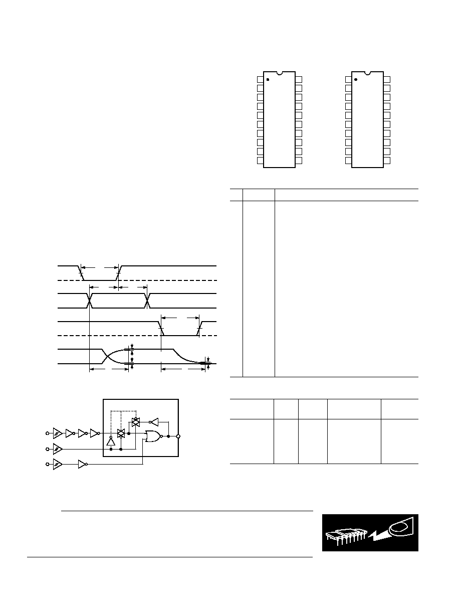
CS
DB11DB0
RS
V
OUT
t
CS
DATA VALID
1
0
0
0
1
1
FS
ZS
t
DS
t
DH
t
RS
0.1% FS
ERROR BAND
t
S
t
S
Figure 3. Timing Diagram
DB
X
CS
RS
TO
INTERNAL
DAC
SWITCHES
1 OF 12 LATCHES
OF THE
DAC REGISTER
Figure 4. Digital Control Logic
WARNING!
ESD SENSITIVE DEVICE
AD7392/AD7393
5
REV. A
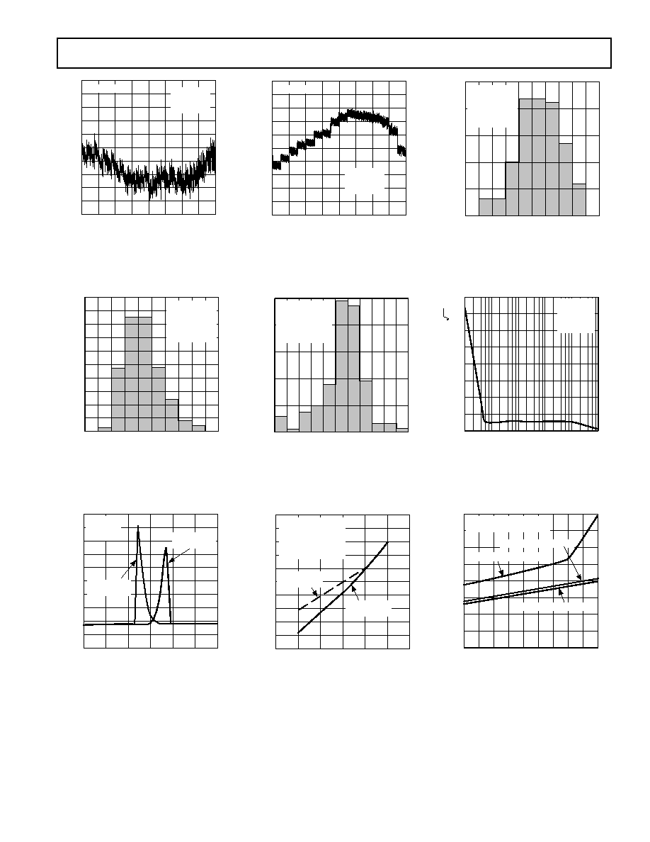
Typical Performance Characteristics
CODE Decimal
1
1
0.4
0.8
0.8
0.6
0.2
0.4
0
0.2
0.6
0
512 1024
4096
1536 2048 2560 3072 3584
V
DD
= 2.7V
V
REF
= 2.5V
T
A
= 25 C
AD7392
INL LSB
Figure 5. AD7392 Integral Nonlinear-
ity Error vs. Code
AD7393
SS = 300 UNITS
T
A
= 25 C
V
DD
= 2.7V
V
REF
= 2.5V
TOTAL UNADJUSTED ERROR LSB
FREQUENCY
100
0
10
40
20
80
60
3.3 3.3 10
16 23
30
36
43
50
90
70
50
30
10
Figure 8. AD7393 Total Unadjusted
Error Histogram
V
IN
Volts
0.0
0.5
3.0
1.0
1.5
2.0
2.5
SUPPLY CURRENT
A
100
95
50
70
65
60
55
90
75
80
85
V
LOGIC
FROM
3.0V TO 0V
V
LOGIC
FROM
0V TO 3.0V
AD7392
T
A
= 25 C
V
DD
= 3.0V
Figure 11. Supply Current vs. Logic
Input Voltage
CODE Decimal
1
1
0.4
0.8
0.8
0.6
0.2
0.4
0
0.2
0.6
0
128
256
1024
384
512
640
768
896
V
DD
= 2.7V
V
REF
= 2.5V
T
A
= 25 C
AD7393
INL LSB
Figure 6. AD7393 Integral Nonlinear-
ity Error vs. Code
FULL SCALE TEMPCO ppm/ C
FREQUENCY
0
66
12
6
24
18
60 52 46 40 32 26 20 12 6
30
0
AD7393
SS = 100 UNITS
T
A
= 40 to 85 C
V
DD
= 2.7V
V
REF
= 2.5V
Figure 9. AD7393 Full-Scale Output
Tempco Histogram
SUPPLY VOLTAGE V
1
2
7
3
4
5
6
THRESHOLD VOLTAGE V
5.0
4.5
0.0
2.0
1.5
1.0
0.5
4.0
2.5
3.0
3.5
V
LOGIC
FROM
HIGH TO LOW
V
LOGIC
FROM
LOW TO HIGH
AD7392
CODE = FFF
H
V
REF
= 2V
RS
LOGIC VOLTAGE
VARIED
Figure 12. Logic Threshold vs.
Supply Voltage
TOTAL UNADJUSTED ERROR LSB
FREQUENCY
25
0
5.0
10
5
20
15
5.8 6.6 7.3 8.1 8.9 9.7 10.5 11.2 12.0
AD7392
SS = 100 UNITS
T
A
= 25 C
V
DD
= 2.7V
V
REF
= 2.5V
Figure 7. AD7392 Total Unadjusted
Error Histogram
FREQUENCY Hz
OUTPUT VOLTAGE NOISE
V/ Hz
10
8
0
1
10
100k
100
1k
10k
6
4
2
12
14
16
AD7392
V
DD
= 5V
V
REF
= 2.5V
T
A
= 25 C
Figure 10. Voltage Noise Density vs.
Frequency
TEMPERATURE C
SUPPLY CURRENT
A
100
20
55
35
125
15
5
25
65
85 105
45
90
60
50
40
30
80
70
AD7392
SAMPLE SIZE = 300 UNITS
V
DD
= 5.0V, V
LOGIC
= 0V
V
DD
= 3.0V, V
LOGIC
= 0V
V
DD
= 3.6V, V
LOGIC
= 2.4V
Figure 13. Supply Current vs.
Temperature
AD7392/AD7393
6
REV. A
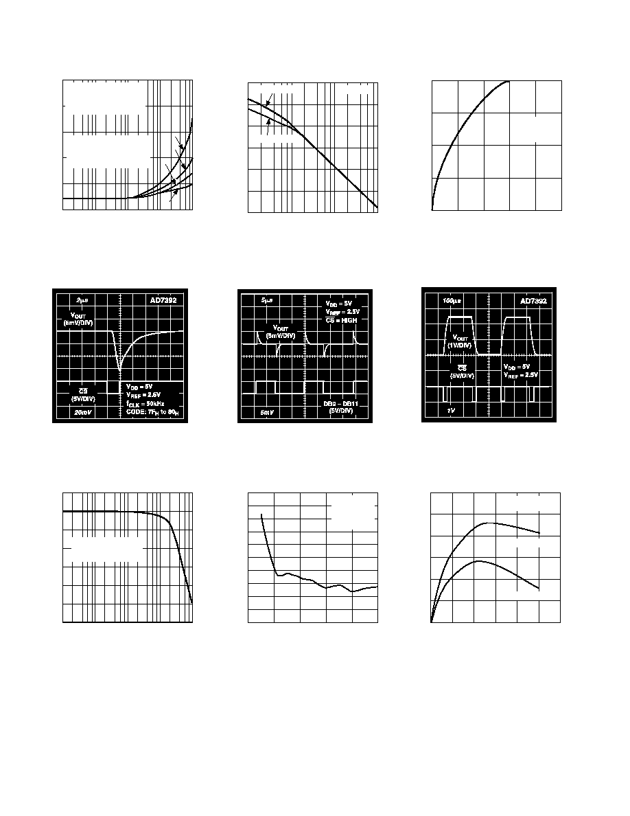
CLOCK FREQUENCY Hz
SUPPLY CURRENT
A
1000
800
0
1k
10k
10M
100k
1M
600
400
200
a. V
DD
= 5.5V, CODE = 155
H
b. V
DD
= 5.5V, CODE = 3FF
H
c. V
DD
= 2.7V, CODE = 155
H
d
. V
DD
= 2.7V, CODE = 355
H
a
b
c
d
AD7393
V
LOGIC
= 0V TO V
DD
TO 0V
V
REF
= 2.5V
T
A
= 25 C
Figure 14. Supply Current vs. Clock
Frequency
TIME 2 s/DIV
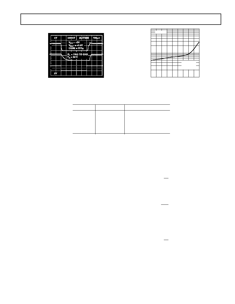
Figure 17. Midscale Transition
Performance
FREQUENCY Hz
GAIN dB
5
0
30
10
100
100k
1k
10k
5
15
25
20
10
V
DD
= +5V
V
REF
= +100mV + 2V
DC
DATA = FFF
H
Figure 20. Reference Multiplying
Bandwidth
FREQUENCY Hz
PSRR dB
60
50
0
10
100
10k
1k
30
20
10
40
V
DD
= 3V 5%
V
DD
= 5V 5%
T
A
= 25 C
Figure 15. Power Supply Rejection
vs. Frequency
TIME 5 s/DIV
Figure 18. Digital Feedthrough
REFERENCE VOLTAGE V
0
5
1
3
2
4
INTEGRAL NONLINEARITY LSB
2.0
1.8
0.0
0.8
0.6
0.4
0.2
1.6
1.0
1.2
1.4
AD7392
V
DD
= +5V
CODE = 768
H
T
A
= 25 C
Figure 21. INL Error vs. Reference
Voltage
V
OUT
V
I
OUT
mA
40
30
0
0
1
5
2
3
4
20
10
V
DD
= +5V
V
REF
= +3V
CODE = ØØØ
H
Figure 16. I
OUT
at Zero Scale vs. V
OUT
TIME 100 s/DIV
Figure 19. Large Signal Settling Time
HOURS OF OPERATION AT 150 C
NOMINAL CHANGE IN VOLTAGE mV
1.2
0.0
0
100
600
200
300
400
500
1.0
0.8
0.6
0.4
0.2
AD7392
SAMPLE SIZE = 50
CODE = FFF
H
CODE = 000
H
Figure 22. Long-Term Drift
Accelerated by Burn-in
AD7392/AD7393
7
REV. A
TIME 100 s/DIV
100
50
0
2
0
1
0
IDD ( A)
V
OUT
(V)
SHDN
100
90
0%
10
Figure 23. Shutdown Recovery Time
Table I. Control Logic Truth Table
CS
RS
DAC Register Function
H
H
Latched
L
H
Transparent
H
Latched with New Data
X
L
Loaded with All Zeros
H
Latched all Zeros
NOTE
Positive logic transition; X Don't Care.
OPERATION
The AD7392 and AD7393 comprise a set of pin compatible,
12-bit/10-bit digital-to-analog converters. These single-supply
operation devices consume less than 100 microamps of current
while operating from power supplies in the +2.7 V to +5.5 V
range making them ideal for battery operated applications. They
contain a voltage-switched, 12-bit/10-bit, laser-trimmed digital-
to-analog converter, rail-to-rail output op amps, and a parallel-
input DAC register. The external reference input has constant
input resistance independent of the digital code setting of the
DAC. In addition, the reference input can be tied to the same
supply voltage as V
DD
, resulting in a maximum output voltage
span of 0 to V
DD
. The parallel data interface consists of 12 data
bits, DB0DB11, for the AD7392; 10 data bits, DB0DB9, for
the AD7393; and a
CS write strobe. A RS pin is available to
reset the DAC register to zero scale. This function is useful for
power-on reset or system failure recovery to a known state.
Additional power savings are accomplished by activating the
SHDN pin, resulting in a 1.5
µ
A maximum consumption sleep
mode. As long as the supply voltage remains, data will be re-
tained in the DAC register to reset the DAC output when the
part is taken out of shutdown (
SHDN = 1).
D/A CONVERTER SECTION
The voltage switched R-2R DAC generates an output voltage
dependent on the external reference voltage connected to the
REF pin according to the following equation:
V
OUT
=
V
REF
×
D
2
N
Equation 1
where D is the decimal data word loaded into the DAC register,
and N is the number of bits of DAC resolution. In the case of
the 10-bit AD7393 using a 2.5 V reference, Equation 1 simpli-
fies to:
V
OUT
=
2.5
×
D
1024
Equation 2
Using Equation 2, the nominal midscale voltage at V
OUT
is 1.25 V
for D = 512; full-scale voltage is 2.497 volts. The LSB step size is
= 2.5
×
1/1024 = 0.0024 volts.
For the 12-bit AD7392 operating from a 5.0 V reference Equa-
tion 1 becomes:
V
OUT
=
V
REF
×
D
2
N
Equation 3
Using Equation 3, the AD7392 provides a nominal midscale
voltage of 2.50 V for D = 2048, and a full-scale output of 4.998
volts. The LSB step size is = 5.0
×
1/4096 = 0.0012 volts.
TEMPERATURE C
SUPPLY CURRENT nA
1000
10
55 35
125
15
65
85
105
5
25
45
100
V
DD
= 5.5V
V
REF
= 2.5V
SHDN
= 0V
AD7392
Figure 24. Shutdown Current vs. Temperature
AD7392/AD7393
8
REV. A
POWER SUPPLY BYPASSING AND GROUNDING
Precision analog products, such as the AD7392/AD7393, require a
well filtered power source. Since the AD7392/AD7393 oper-
ate from a single +3 V to +5 V supply, it seems convenient to
simply tap into the digital logic power supply. Unfortunately,
the logic supply is often a switch-mode design, which generates
noise in the 20 kHz to 1 MHz range. In addition, fast logic gates
can generate glitches of hundreds of millivolts in amplitude due
to wiring resistance and inductance. The power supply noise
generated as a result means that special care must be taken to
assure that the inherent precision of the DAC is maintained.
Good engineering judgment should be exercised when address-
ing the power supply grounding and bypassing of the AD7392.
The AD7392 should be powered directly from the system power
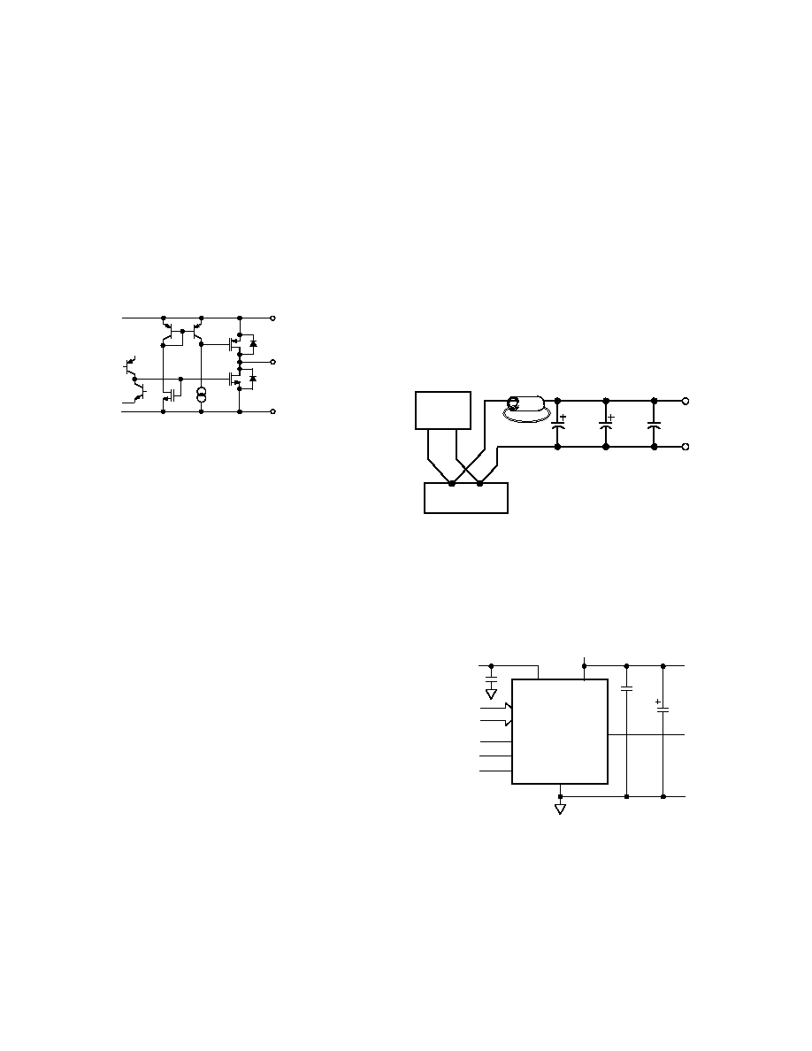
supply. This arrangement, shown in Figure 26, employs an LC
filter and separate power and ground connections to isolate the
analog section from the logic switching transients.
100 F
ELECT.
10-22 F
TANT.
0.1 F
CER.
TTL/CMOS
LOGIC
CIRCUITS
+5V
POWER SUPPLY
+5V
+5V
RETURN
FERRITE BEAD:
2 TURNS, FAIR-RITE
#2677006301
Figure 26. Use Separate Traces to Reduce Power Supply
Noise
Whether or not a separate power supply trace is available, gener-
ous supply bypassing will reduce supply line induced errors.
Local supply bypassing, consisting of a 10
µ
F tantalum electro-
lytic in parallel with a 0.1
µ
F ceramic capacitor, is recom-
mended in all applications (Figure 27).
V
OUT
CS
1
20
19
17, 18
4
3
2
C
*
RS
DB0DB11
+2.7V TO +5.5V
V
DD
REF
GND
SHDN
AD7392
OR
AD7393
0.1 F
10 F
* OPTIONAL EXTERNAL
REFERENCE BYPASS
Figure 27. Recommended Supply Bypassing for the
AD7392/AD7393
AMPLIFIER SECTION
The internal DAC's output is buffered by a low power con-
sumption precision amplifier. The op amp has a 60
µ
s typical
settling time to 0.1% of full scale. There are slight differences in
settling time for negative slewing signals versus positive. Also,
negative transition settling-time to within the last 6 LSBs of
zero volts has an extended settling time. The rail-to-rail output
stage of this amplifier has been designed to provide precision
performance while operating near either power supply. Figure
25 shows an equivalent output schematic of the rail-to-rail-
amplifier with its N-channel pull-down FETs that will pull an
output load directly to GND. The output sourcing current is
provided by a P-channel pull-up device that can source current
to GND terminated loads.
P-CH
N-CH
V
DD
V
OUT
AGND
Figure 25. Equivalent Analog Output Circuit
The rail-to-rail output stage provides
±
1 mA of output current.
The N-channel output pull-down MOSFET, shown in Figure
25, has a 35
ON resistance that sets the sink current capability
near ground. In addition to resistive load driving capability, the
amplifier also has been carefully designed and characterized for
up to 100 pF capacitive load driving capability.
REFERENCE INPUT
The reference input terminal has a constant input resistance
independent of digital code, which results in reduced glitches
on the external reference voltage source. The high 2.5 M
input-resistance minimizes power dissipation within the
AD7392/AD7393 D/A converters. The V
REF
input accepts
input voltages ranging from ground to the positive-supply volt-
age V
DD
. One of the simplest applications that saves an external
reference voltage source is connection of the REF terminal to
the positive V
DD
supply. This connection results in a rail-to-rail
voltage output span maximizing the programmed range. The
reference input will accept ac signals as long as they are kept
within the supply voltage range, 0 < V
REF IN
< V
DD
. The refer-
ence bandwidth and integral nonlinearity error performance are
plotted in the typical performance section (see Figures 20 and
21). The ratiometric reference feature makes the AD7392/
AD7393 an ideal companion to ratiometric analog-to-digital
converters such as the AD7896.
POWER SUPPLY
The very low power consumption of the AD7392/AD7393 is a
direct result of a circuit design optimizing the use of a CBCMOS
process. By using the low power characteristics of CMOS for
the logic and the low noise, tight-matching of the complemen-
tary bipolar transistors, excellent analog accuracy is achieved.
One advantage of the rail-to-rail output amplifiers used in the
AD7392/AD7393 is the wide range of usable supply voltage.
The part is fully specified and tested for operation from +2.7 V
to +5.5 V.
AD7392/AD7393
9
REV. A
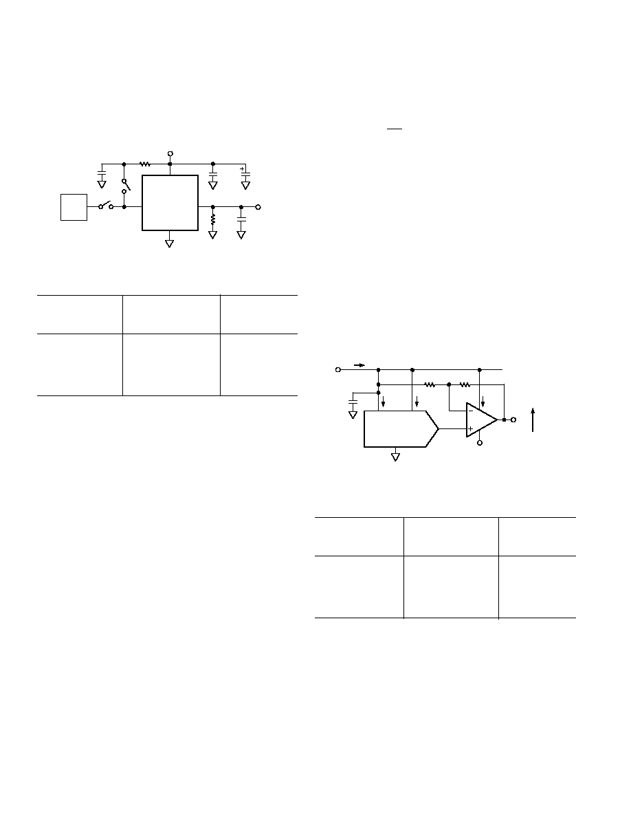
RESET (
RS) PIN
Forcing the asynchronous
RS pin low will set the DAC register
to all zeros and the DAC output voltage will be zero volts. The
reset function is useful for setting the DAC outputs to zero at
power-up or after a power supply interruption. Test systems and
motor controllers are two of many applications that benefit from
powering up to a known state. The external reset pulse can be
generated by the microprocessor's power-on RESET signal, by
an output from the microprocessor or by an external resistor
and capacitor. RESET has a Schmitt trigger input which results
in a clean reset function when using external resistor/capacitor
generated pulses. See the Control-Logic Truth Table I.
POWER SHUTDOWN (
SHDN)
Maximum power savings can be achieved by using the power
shutdown control function. This hardware activated feature is
controlled by the active low input
SHDN pin. This pin has a
Schmitt trigger input that helps desensitize it to slowly changing
inputs. By placing a logic low on this pin, the internal consump-
tion of the AD7392 or AD7393 is reduced to nanoamp levels,
guaranteed to 1.5
µ
A maximum over the operating temperature
range. If power is present at all times on the V
DD
pin while in
the shutdown mode, the internal DAC register will retain the
last programmed data value. The digital interface is still active
in shutdown, so that code changes can be made that will pro-
duce new DAC settings when the device is taken out of shut-
down. This data will be used when the part is returned to the
normal active state by placing the DAC back to its programmed
voltage setting. Figure 23 shows a plot of shutdown recovery
time with both I
DD
and V
OUT
displayed. In the shutdown state
the DAC output amplifier exhibits an open-circuit high resis-
tance state. Any load connected will stabilize at its termination
voltage. If the power shutdown feature is not needed, the user
should tie the
SHDN pin to the V
DD
voltage thereby disabling
this function.
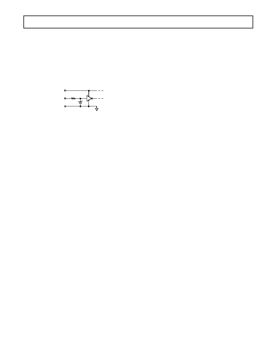
INPUT LOGIC LEVELS
All digital inputs are protected with a Zener-type ESD protec-
tion structure (Figure 28) that allows logic input voltages to
exceed the V
DD
supply voltage. This feature can be useful if the
user is driving one or more of the digital inputs with a 5 V
CMOS logic input-voltage level while operating the AD7392/
AD7393 on a +3 V power supply. If this mode of interface is
used, make sure that the V
OL
of the 5 V CMOS meets the V
IL
input requirement of the AD7392/AD7393 operating at 3 V.
See Figure 12 for a graph for digital logic input threshold versus
operating V
DD
supply voltage.
V
DD
LOGIC
IN
GND
1k
Figure 28. Equivalent Digital Input ESD Protection
In order to minimize power dissipation from input-logic levels
that are near the V
IH
and V
IL
logic input voltage specifications, a
Schmitt trigger design was used that minimizes the input-buffer
current consumption compared to traditional CMOS input
stages. Figure 11 shows a plot of incremental input voltage
versus supply current, showing that negligible current consump-
tion takes place when logic levels are in their quiescent state.
The normal cross over current still occurs during logic transi-
tions. A secondary advantage of this Schmitt trigger is the pre-
vention of false triggers that would occur with slow moving logic
transitions when a standard CMOS logic interface or opto-
isolators are used. The logic inputs DB11DB0,
CS, RS, SHDN
all contain the Schmitt trigger circuits.
DIGITAL INTERFACE
The AD7392/AD7393 have a parallel data input. A functional
block diagram of the digital section is shown in Figure 4, while
Table I contains the truth table for the logic control inputs.
The chip select (
CS) pin controls loading of data from the data
inputs on pins DB11DB0. This active low input places the
input register into a transparent state allowing the data inputs to
directly change the DAC ladder values. When
CS returns to
logic high within the data setup and hold time specifications, the
new value of data in the input-register will be latched. See Truth
Table for complete set of conditions.
AD7392/AD7393
10
REV. A
UNIPOLAR OUTPUT OPERATION
This is the basic mode of operation for the AD7392. As shown
in Figure 29, the AD7392 has been designed to drive loads as
low as 5 k
in parallel with 100 pF. The code table for this
operation is shown in Table II.
1
20
19
17, 18
0.01 F
+2.7V TO +5.5V
V
DD
AGND/DGND
AD7392
0.1 F
10 F
DIGITAL INTERFACE
CIRCUITRY OMITTED
FOR CLARITY
V
OUT
R
L
5k
C
L
100pF
REF
EXT
REF
R
Figure 29. AD7392 Unipolar Output Operation
Table II. Unipolar Code Table
Hexadecimal
Decimal
Output
Number
Number
Voltage (V)
in DAC Register
in DAC Register
V
REF
= 2.5 V
FFF
4095
2.4994
801
2049
1.2506
800
2048
1.2500
7FF
2047
1.2494
000
0
0
The circuit can be configured with an external reference plus
power supply or powered from a single dedicated regulator
or reference depending on the application performance re-
quirements.
BIPOLAR OUTPUT OPERATION
Although the AD7393 has been designed for single-supply op-
eration, the output can be easily configured for bipolar opera-
tion. A typical circuit is shown in Figure 30. This circuit uses a
clean regulated +5 V supply for power, which also provides the
circuit's reference voltage. Since the AD7393 output span swings
from ground to very near +5 V, it is necessary to choose an exter-
nal amplifier with a common-mode input voltage range that
extends to its positive supply rail. The micropower consump-
tion OP196 has been designed just for this purpose and results
in only 50 microamps of maximum current consumption. Con-
nection of the equal valued 470 k
resistors results in a differen-
tial amplifier mode of operation with a voltage gain of two,
which produces a circuit output span of ten volts (that is, 5 V
to +5 V). As the DAC is programmed from zero-code 000
H
to
midscale 200
H
to full scale 3FF
H
, the circuit output voltage V
O
is set at 5 V, 0 V and +5 V (minus 1 LSB). The output voltage
V
O
is coded in offset binary according to Equation 4.
V
O
=
D
512
1
×
5
Equation 4
where D is the decimal code loaded in the AD7393 DAC regis-
ter. Note that the LSB step size is 10/1024 = 10 mV. This cir-
cuit has been optimized for micropower consumption including
the 470 k
gain setting resistors, which should have low tem-
perature coefficients to maintain accuracy and matching (prefer-
ably the same resistor material, such as metal film). If better
stability is required, the power supply could be substituted with
a precision reference voltage such as the low drop out REF195,
which can easily supply the circuit's 162
µ
A of current, and still
provide additional power for the load connected to V
O
. The
micropower REF195 is guaranteed to source 10 mA output
drive current, but only consumes 50
µ
A internally. If higher
resolution is required, the AD7392 can be used with the addi-
tion of two more bits of data inserted into the software coding,
which would result in a 2.5 mV LSB step size. Table III shows
examples of nominal output voltages V
O
provided by the Bipolar
Operation circuit application.
V
O
C
V
DD
REF
GND
<100 A
<2 A
470k
+5V
I
SY
< 162 A
OP196
470k
+5V
5V
BIPOLAR
OUTPUT
SWING
5V
AD7393
DIGITAL INTERFACE CIRCUITRY OMITTED FOR CLARITY
V
OUT
<50 A
Figure 30. Bipolar Output Operation
Table III. Bipolar Code Table
Hexadecimal
Decimal
Analog
Number
Number
Output
In DAC Register
in DAC Register
Voltage (V)
3FF
1023
4.9902
201
513
0.0097
200
512
0.0000
1FF
511
0.0097
000
0
5.0000
AD7392/AD7393
11
REV. A
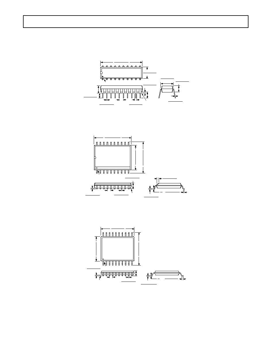
OUTLINE DIMENSIONS
Dimensions shown in inches and (mm).
20-Lead Plastic DIP Package
(N-20)
20
1
10
11
1.060 (26.90)
0.925 (23.50)
0.280 (7.11)
0.240 (6.10)
PIN 1
SEATING
PLANE
0.022 (0.558)
0.014 (0.356)
0.210 (5.33)
MAX
0.130
(3.30)
MIN
0.070 (1.77)
0.045 (1.15)
0.100
(2.54)
BSC
0.160 (4.06)
0.115 (2.93)
0.060 (1.52)
0.015 (0.38)
0.325 (8.25)
0.300 (7.62)
0.015 (0.381)
0.008 (0.204)
0.195 (4.95)
0.115 (2.93)
20-Lead SOIC Package
(R-20)
SEATING
PLANE
0.0118 (0.30)
0.0040 (0.10)
0.0192 (0.49)
0.0138 (0.35)
0.1043 (2.65)
0.0926 (2.35)
0.0500
(1.27)
BSC
0.0125 (0.32)
0.0091 (0.23)
0.0500 (1.27)
0.0157 (0.40)
8
°
0
°
0.0291 (0.74)
0.0098 (0.25)
x 45
°
20
11
10
1
0.5118 (13.00)
0.4961 (12.60)
0.4193 (10.65)
0.3937 (10.00)
0.2992 (7.60)
0.2914 (7.40)
PIN 1
20-Lead Thin Surface Mount TSSOP Package
(RU-20)
20
11
10
1
0.260 (6.60)
0.252 (6.40)
0.256 (6.50)
0.246 (6.25)
0.177 (4.50)
0.169 (4.30)
PIN 1
SEATING
PLANE
0.006 (0.15)
0.002 (0.05)
0.0118 (0.30)
0.0075 (0.19)
0.0256 (0.65)
BSC
0.0433
(1.10)
MAX
0.0079 (0.20)
0.0035 (0.090)
0.028 (0.70)
0.020 (0.50)
8
°
0
°
C2210a23/99
PRINTED IN U.S.A.