 | ÐлекÑÑоннÑй компоненÑ: AD75019 | СкаÑаÑÑ:  PDF PDF  ZIP ZIP |
Äîêóìåíòàöèÿ è îïèñàíèÿ www.docs.chipfind.ru
REV. C
Information furnished by Analog Devices is believed to be accurate and
reliable. However, no responsibility is assumed by Analog Devices for its
use, nor for any infringements of patents or other rights of third parties
which may result from its use. No license is granted by implication or
otherwise under any patent or patent rights of Analog Devices.
a
AD75019
One Technology Way, P.O. Box 9106, Norwood, MA 02062-9106, U.S.A.
Tel: 781/329-4700
World Wide Web Site: http://www.analog.com
Fax: 781/326-8703
© Analog Devices, Inc., 1999
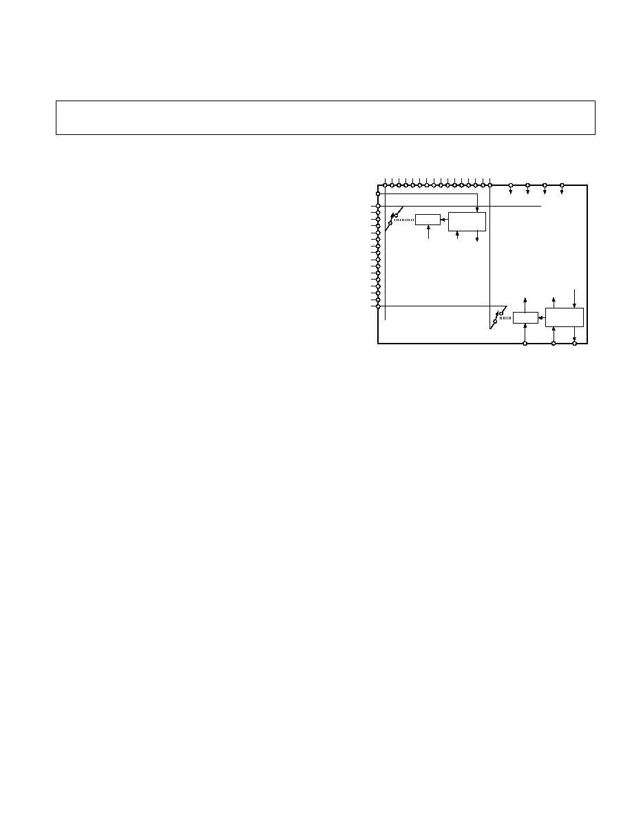
16 16 Crosspoint
Switch Array
FUNCTIONAL BLOCK DIAGRAM
SHIFT
REGISTER
CELL #256
LATCH
SERIAL DATA IN
ANALOG
SWITCH
BUSED CLOCK
LINES
SERIAL
DATA
TO NEXT
STAGES
+12V 12V
+5V
DGND
AD75019
16 16 ARRAY OF SWITCHES,
LATCHES, AND SHIFT REGISTER
CELLS (ONLY TWO LOCATIONS
ARE SHOWN FOR CLARITY)
SHIFT
REGISTER
CELL #1
LATCH
ANALOG
SWITCH
PARALLEL
CLOCK
SERIAL
CLOCK
SERIAL
DATA
FROM
PRIOR
STAGES
BUSED CLOCK
LINES
V
DD
V
SS
V
CC
DGND
X0
X15
ANALOG
INPUTS/OUTPUTS
Y0
Y15
ANALOG
OUTPUTS/
INPUTS
PCLK
SCLK
SOUT
FEATURES
256 Switches in a 16 16 Array
Wide Signal Range: to Supply Rails of 24 V or 12 V
Low On-Resistance: 200
Typ
TTL/CMOS/Microprocessor-Compatible Control Lines
Serial Input Simplifies Interface
Serial Output Allows Cascading for More Channels
Low Power Consumption: 2 mW Quiescent
Compact 44-Lead PLCC
PRODUCT DESCRIPTION
The AD75019 contains 256 analog switches in a 16
×
16 array.
Any of the X or Y pins may serve as an input or output. Any or
all of the X terminals may be programmed to connect to any or
all of the Y terminals. The switches can accommodate signals
with amplitudes up to the supply rails and have a typical on-
resistance of 150
.
Data is loaded serially via the SIN input and clocked into an on-
board 256-bit shift register via SCLK. When all the switch set-
tings have been programmed, data is transferred into a set of
256 latches via PCLK. The serial shift register is dynamic, so
there is a minimum clock rate of 20 kHz. The maximum clock
rate of 5 MHz allows loading times as short as 52
µ
s. The switch
control latches are static and will hold their data as long as power
is applied.
To extend the number of switches in the array, you may cascade
multiple AD75019s. The SOUT output is the end of the shift
register, and may be connected to the SIN input of the next
AD75019.
The AD75019 is fabricated in Analog Devices' BiMOS II
process. This epitaxial BiCMOS process features CMOS
devices for low distortion switches and bipolar devices for
ESD protection.
REV. C
2
AD75019SPECIFICATIONS
1
AD75019
Symbol
Min
Typ
Max
Units
MULTIPLEXER
Input Signal Range
V
IN
V
SS
0.5
V
DD
+ 0.5
V
Switch ON Resistance, V
DD
and V
SS
=
±
12 V, V
SIGNAL
=
±
12 V
R
ON
150
300
Switch ON Resistance, V
DD
and V
SS
=
±
5 V, V
SIGNAL
=
±
5 V
R
ON
300
500
Switch ON Resistance Matching
2
, V
SIGNAL
=
±
12 V
R
ON
20
30
Leakage Current, V
SIGNAL
=
±
10 V
2
10
nA
Input/Output Capacitance
C
IN
25
pF
Isolation Between Any Two Channels
R
S
= 600
, R
L
= 10 k
, V
SIGNAL
= 2 V p-p
f
SIGNAL
= 1 kHz
92
dB
f
SIGNAL
= 20 kHz
69
dB
f
SIGNAL
= 1 MHz
38
dB
Total Harmonic Distortion
R
S
= 600
, R
L
= 10 k
, V
SIGNAL
= 2 V p-p
0.01
%
Switch Frequency Response, 3 dB
R
S
= 600
, R
L
= 10 k
, V
SIGNAL
= 2 V p-p
20
MHz
Propagation Delay
4
8
ns
DIGITAL INPUTS (SIN, SCLK, PCLK)
Logic Levels (TTL Compatible)
Input Voltage, Logic "1"
V
IH
2.4
5.5
V
Input Voltage, Logic "0"
V
IL
0
0.8
V
Input Current, V
IH
= 5.5 V
I
IH
±
1
µ
A
Input Current, V
IL
= 0.8 V
I
IL
±
1
µ
A
Input Capacitance
C
IN
10
pF
DIGITAL OUTPUTS (SOUT)
Logic Levels (TTL Compatible)
Output Voltage, Logic "1"
V
OH
2.8
V
Output Voltage, Logic "0"
V
OL
0.4
V
Output Current, V
OH
= 2.8 V
I
OH
3.2
mA
Output Current, V
OL
= 0.4 V
I
OL
3.2
mA
POWER SUPPLY REQUIREMENTS
Voltage Range, Total Analog
V
DD
V
SS
9.0
25.2
V
Voltage Range, Positive Analog
V
DD
V
DGND
(V
CC
0.5)
25.2
V
Voltage Range, Negative Analog
V
SS
V
DGND
20.7
0
V
Voltage Range, Digital
V
CC
V
DGND
4.5
5
5.5
V
Supply Current, SCLK = 5 MHz,
I
DD
, I
SS
±
70
mA
V
IL
= 0.8 V, V
IH
= 2.4 V
I
CC
800
µ
A
Supply Current, Quiescent,
I
DD
, I
SS
_
400
µ
A
V
IL
= 0.8 V, V
IH
= 2.4 V
I
CC
_
100
µ
A
TEMPERATURE RANGE
Operating
T
MIN
, T
MAX
25
+85
°
C
Storage
65
+150
°
C
NOTES
1
All minimum and maximum specifications are guaranteed, and specifications shown in boldface are tested on all production units at final electrical test. Results from those tests
are used to calculate outgoing quality levels.
2
Switch resistance matching is measured with zero volts at each analog input and refers to the difference between the maximum and minimum values.
Specifications subject to change without notice.
(T
A
= +25 C, V
DD
and V
SS
= 12 V, V
CC
= +5 V unless otherwise noted)
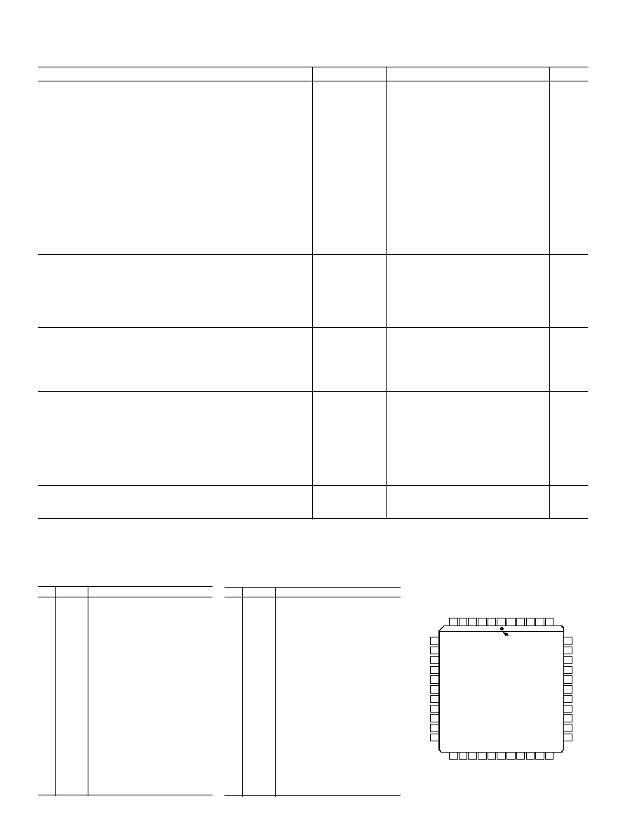
PIN CONFIGURATION
6 5 4 3 2 1 44 43 42 41 40
PIN 1
IDENTIFIER
TOP VIEW
(Not to Scale)
39
38
37
36
35
34
33
32
31
30
29
7
8
9
10
11
12
13
14
15
16
17
18 19 20 21 22 23 24 25 26 27 28
NC = NO CONNECT
NC
Y7
Y6
Y5
Y4
Y3
Y2
Y1
Y0
X15
X14
Y15
Y14
Y13
Y12
Y11
Y10
Y9
Y8
X0
X1
X2
NC
NC
V
SS
SIN
SCLK
PCLK
SOUT
X3
X4
X5
X6
X8
X9
X10
X11
X12
X13
X7
DGND
V
CC
V
DD
NC
AD75019
PIN FUNCTION DESCRIPTIONS
Pin
Name
Description
1
PCLK
Parallel Clock Input
2
SCLK
Serial Clock Input
3
SIN
Serial Data Input
4
V
SS
Negative Analog Power Supply
5
NC
No Internal Connection
6
NC
No Internal Connection
7
Y15
Analog Output (or Input)
8
Y14
Analog Output (or Input)
9
Y13
Analog Output (or Input)
10
Y12
Analog Output (or Input)
11
Y11
Analog Output (or Input)
12
Y10
Analog Output (or Input)
13
Y9
Analog Output (or Input)
14
Y8
Analog Output (or Input)
15
X0
Analog Input (or Output)
16
X1
Analog Input (or Output)
17
X2
Analog Input (or Output)
18
X3
Analog Input (or Output)
19
X4
Analog Input (or Output)
20
X5
Analog Input (or Output)
21
X6
Analog Input (or Output)
22
X7
Analog Input (or Output)
Pin
Name
Description
23
X8
Analog Input (or Output)
24
X9
Analog Input (or Output)
25
X10
Analog Input (or Output)
26
X11
Analog Input (or Output)
27
X12
Analog Input (or Output)
28
X13
Analog Input (or Output)
29
X14
Analog Output (or Input)
30
X15
Analog Output (or Input)
31
Y0
Analog Output (or Input)
32
Y1
Analog Output (or Input)
33
Y2
Analog Output (or Input)
34
Y3
Analog Output (or Input)
35
Y4
Analog Output (or Input)
36
Y5
Analog Output (or Input)
37
Y6
Analog Output (or Input)
38
Y7
Analog Output (or Input)
39
NC
No Internal Connection
40
NC
No Internal Connection
41
V
DD
Positive Analog Power Supply
42
V
CC
Digital Power Supply
43
DGND Digital Ground
44
SOUT
Serial Data Output: Positive True
REV. C
AD75019
3
(T
A
= T
MIN
to T
MAX
, rated power supplies unless otherwise noted)
TIMING CHARACTERISTICS
1
Parameter
Symbol
Value
Units
Condition
Data Setup Time
t
1
20
ns
min
SCLK Pulsewidth
t
2
100
ns
min
Data Hold Time
t
3
40
ns
min
SCLK Pulse Separation
t
4
100
ns
min
SCLK to PCLK Delay
t
5
65
ns
min
SCLK to PCLK Delay and Release
(t
5
+ t
6
)
5
ms
max
PCLK Pulsewidth
t
6
65
ns
min
Propagation Delay, PCLK to Switches On or Off
_
70
ns
max
Data Load Time
_
52
µ
s
SCLK = 5 MHz
SCLK Frequency
_
20
kHz
min
SCLK, PCLK Rise and Fall Times
_
1
µ
s
max
NOTES
1
Timing measurement reference level is 1.5 V.
Specifications subject to change without notice.
OPERATION TRUTH TABLE
Control Lines
PCLK
SCLK
SIN
SOUT
Operation/Comment
1
0
X
X
No operation.
1
1
Data
i
Data
i-256
The data on the SIN line is loaded into the serial register; data clocked into the
serial register 256 clocks ago appears at the SOUT output.
0
X
X
X
Data in the serial shift register transfers into the parallel latches which control the
switch array.
APPLICATIONS INFORMATION
Loading Data
Data to control the switches is clocked serially into a 256-bit
shift register and then transferred in parallel to 256 bits of mem-
ory. The rising edge of SCLK, the serial clock input, loads data
into the shift register. The first bit loaded via SIN, the serial
data input, controls the switch at the intersection of row Y15
and column X15. The next bits control the remaining columns
(down to X0) of row Y15, and are followed by the bits for row
Y14, and so on down to the data for the switch at the intersec-
tion of row Y0 and column X0. The shift register is dynamic, so
there is a minimum clock rate, specified as 20 kHz.
After the shift register is filled with the new 256 bits of control
data, PCLK is activated (pulsed low) to transfer the data to the
parallel latches. Since the shift register is dynamic, there is a
maximum time delay specified before the data is lost: PCLK
must be activated and brought back high within 5 ms after fill-
ing the shift register. The switch control latches are static and
will hold their data as long as power is applied.
To extend the number of switches in the array, you may cascade
multiple AD75019s. The SOUT output is the end of the shift
register, and may be directly connected to the SIN input of the
next AD75019.
Power Supply Sequencing and Bypassing
All junction-isolated parts operating on multiple power supplies
require proper attention to supply sequencing. Because BiMOS
II is a junction-isolated process, parasitic diodes exist between
V
DD
and V
CC
, and between V
SS
and DGND. As a result, V
DD
must always be greater than (V
CC
0.5 V), and V
SS
must always
be less than (DGND + 0.5 V).
If you can't ensure that system power supplies will sequence to
meet these conditions, external Schottky (e.g., 1N5818) or
silicon (e.g., 1N4001) diodes may be used. To protect the posi-
tive side, the anode would connect to V
CC
(Pin 42) and the
cathode to V
DD
(Pin 41). For the negative side, connect the
anode to V
SS
(Pin 4) and the cathode to DGND (Pin 43).
Each of the three power supply pins [V
DD
(Pin 41), V
CC
(Pin
42) and V
SS
(Pin 4)] should be bypassed to DGND (Pin 43)
through a 0.1
µ
F ceramic capacitor located close to the package
pins.
Transistor Count
AD75019 contains 5,472 transistors. This number may be used
for calculating projected reliability.
TIMING DIAGRAM
Y0X0
Y15X14
t
6
Y15X15
t
2
1
0
1
0
SCLK
PCLK
1 = CLOSE
0 = OPEN
SIN
TRANSFER DATA FROM SERIAL
REGISTER TO PARALLEL
LATCHES DURING LOW LEVEL
t
5
t
1
t
3
t
4
LOAD DATA INTO
SERIAL REGISTER
DURING RISING EDGE
REV. C
AD75019
4
ABSOLUTE MAXIMUM RATINGS*
Min
Max
Units
Conditions
V
DD
to DGND
0.5
+25.2
V
V
SS
to DGND
25.2
+0.5
V
V
CC
to DGND
0.5
+7.0
V
V
DD
to V
SS
0.5
+25.2
V
V
CC
to V
SS
0.5
+25.2
V
Digital Inputs to DGND
0.3
V
CC
+ 0.5
V
Power Dissipation
1.0
W
T
A
75
°
C
Operating Temperature Range
0
+70
°
C
Storage Temperature
65
+150
°
C
Lead Temperature
+300
°
C
Soldering, 10 sec
*Stresses above those listed under Absolute Maximum Ratings may cause permanent damage to the device. These are stress
ratings only; functional operation of the device at these or any other conditions above those indicated in the operational
sections of this specification is not implied. Exposure to absolute maximum rating conditions for extended periods may affect
device reliability.
CAUTION
ESD (electrostatic discharge) sensitive device. The digital control inputs are Zener protected;
however, permanent damage may occur on unconnected devices subject to high energy
electrostatic fields. Unused devices must be stored in conductive foam or shunts. The protective
foam should be discharged to the destination socket before devices are removed.
WARNING!
ESD SENSITIVE DEVICE
ORDERING GUIDE
Model
Temperature Range
Package Option*
AD75019JP
0
°
C to +70
°
C
P-44A
*P = Plastic Leaded Chip Carrier (PLCC) Package.
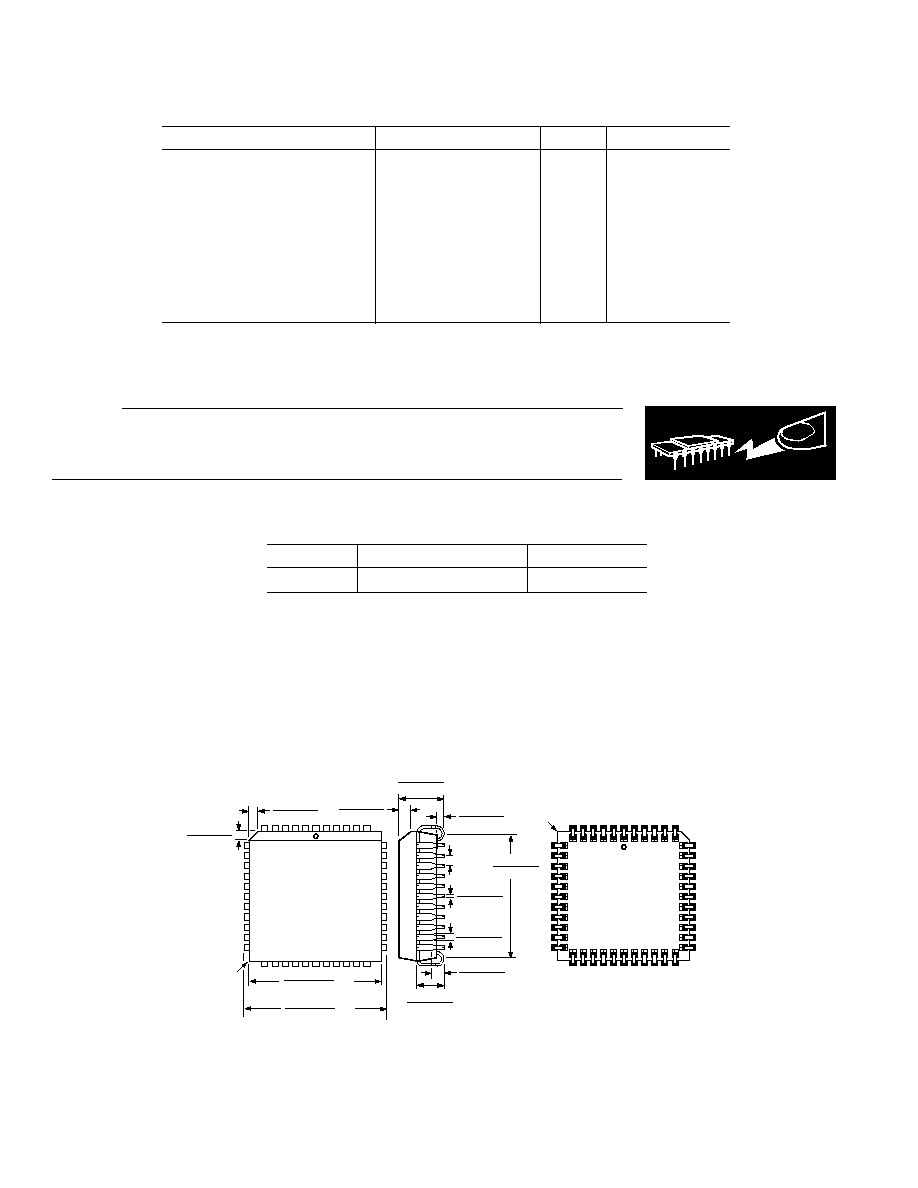
OUTLINE DIMENSIONS
Dimensions shown in inches and (mm).
44-Lead Plastic Leaded Chip Carrier
(P-44A)
PIN 1
IDENTIFIER
BOTTOM VIEW
(PINS UP)
0.020
(0.50)
R
6
PIN 1
IDENTIFIER
7
40
39
17
18
29
28
TOP VIEW
(PINS DOWN)
0.695 (17.65)
0.685 (17.40)
SQ
0.656 (16.66)
0.650 (16.51)
SQ
0.048 (1.21)
0.042 (1.07)
0.048 (1.21)
0.042 (1.07)
0.020
(0.50)
R
0.021 (0.53)
0.013 (0.33)
0.050
(1.27)
BSC
0.63 (16.00)
0.59 (14.99)
0.032 (0.81)
0.026 (0.66)
0.180 (4.57)
0.165 (4.19)
0.040 (1.01)
0.025 (0.64)
0.056 (1.42)
0.042 (1.07)
0.025 (0.63)
0.015 (0.38)
0.110 (2.79)
0.085 (2.16)
C1502c08/99
PRINTED IN U.S.A.