 | ÐлекÑÑоннÑй компоненÑ: AD7643 | СкаÑаÑÑ:  PDF PDF  ZIP ZIP |
AD7643 18-Bit, 1.25 MSPS PulSAR® ADC Data Sheet (Rev. 0)
18-Bit, 1.25 MSPS PulSAR
®
ADC
AD7643
Rev. 0
Information furnished by Analog Devices is believed to be accurate and reliable. However, no
responsibility is assumed by Analog Devices for its use, nor for any infringements of patents or other
rights of third parties that may result from its use. Specifications subject to change without notice. No
license is granted by implication or otherwise under any patent or patent rights of Analog Devices.
Trademarks and registered trademarks are the property of their respective owners.
One Technology Way, P.O. Box 9106, Norwood, MA 02062-9106, U.S.A.
Tel: 781.329.4700
www.analog.com
Fax: 781.461.3113
©2006 Analog Devices, Inc. All rights reserved.
FEATURES
Throughput: 1.25 MSPS
INL: ±1.5 LSB typical, ±3 LSB maximum (±11 ppm of full scale)
18-bit resolution with no missing codes
Dynamic range: 95 dB typical
SINAD: 93.5 dB typical @ 20 kHz (V
REF
= 2.5 V)
THD: -113 dB typical @ 20 kHz (V
REF
= 2.5 V)
2.048 V internal reference: typical drift 8 ppm/°C; TEMP output
Differential input range: ±V
REF
(V
REF
up to 2.5 V)
No pipeline delay (SAR architecture)
Parallel (18-, 16-, or 8-bit bus) and serial 5 V/3.3 V/2.5 V interface
SPI®/QSPITM/MICROWIRETM/DSP compatible
Single 2.5 V supply operation
Power dissipation
65 mW typical @ 1.25 MSPS with internal REF
2 W in power-down mode
Pb-free, 48-lead LQFP and 48-lead LFCSP_VQ
Pin compatible with the
AD7641
and other PulSAR ADC's
APPLICATIONS
Medical instruments
High speed data acquisition/high dynamic data acquisition
Digital signal processing
Spectrum analysis
Instrumentation
Communications
ATE
GENERAL DESCRIPTION
The AD7643 is an 18-bit, 1.25 MSPS, charge redistribution
SAR, fully differential, analog-to-digital converter (ADC) that
operates from a single 2.5 V power supply. The part contains a
high speed, 18-bit sampling ADC, an internal conversion clock,
an internal reference (and buffer), error correction circuits, and
both serial and parallel system interface ports. The part has no
latency and can be used in asynchronous rate applications. The
AD7643 is hardware factory calibrated and tested to ensure ac
parameters, such as signal-to-noise ratio (SNR), in addition to
the more traditional dc parameters of gain, offset, and linearity.
The AD7643 is only available in Pb-free packages with
operation specified from -40°C to +85°C.
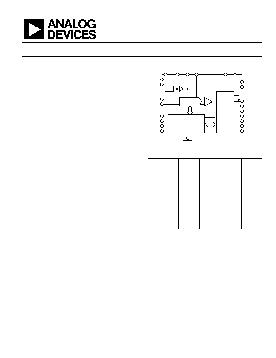
FUNCTIONAL BLOCK DIAGRAM
18
CONTROL LOGIC AND
CALIBRATION CIRCUITRY
CLOCK
AD7643
DGND
DVDD
AVDD
AGND
REF REFGND
IN+
IN
PD
RESET
PDBUF
REFBUFIN
PDREF
REF
TEMP
D[17:0]
BUSY
RD
CS
D0/OB/2C
OGND
OVDD
MODE1
MODE0
REF AMP
CNVST
SERIAL
PORT
PARALLEL
INTERFACE
SWITCHED
CAP DAC
06
024
-
001
Figure 1.
Table 1. PulSAR 48-Lead Selection
Type/kSPS
100 to
250
500 to
570
650 to
1000 >1000
Pseudo
Differential
AD7651
,
AD7660
,
AD7661
AD7650
,
AD7652,
AD7664
,
AD7666
AD7653
,
AD7667
True Bipolar
AD7610
,
AD7663
AD7665
AD7612
,
AD7671
True
Differential
AD7675
AD7676
AD7677
AD7621
,
AD7622,
AD7623
18-Bit
Multichannel/
AD7631
,
AD7678
AD7679
AD7634
,
AD7674
AD7641
,
AD7643
Simultaneous
AD7654
AD7655
PRODUCT HIGHLIGHTS
1.
Fast Throughput.
The AD7643 is a 1.25 MSPS, charge redistribution,
18-bit SAR ADC.
2.
Superior Linearity.
The AD7643 has no missing 18-bit code.
3.
Internal Reference.
The AD7643 has a 2.048 V internal reference with a typical
drift of ±8 ppm/°C and an on-chip TEMP sensor.
4.
Single-Supply Operation.
The AD7643 operates from a 2.5 V single supply.
5.
Serial or Parallel Interface.
Versatile parallel (18-, 16-, or 8-bit bus) or 2-wire serial
interface arrangement compatible with 2.5 V, 3.3 V, or
5 V logic.

AD7643
Rev. 0 | Page 2 of 28
TABLE OF CONTENTS
Features .............................................................................................. 1
Applications....................................................................................... 1
General Description ......................................................................... 1
Functional Block Diagram .............................................................. 1
Product Highlights ........................................................................... 1
Revision History ............................................................................... 2
Specifications..................................................................................... 3
Timing Specifications....................................................................... 5
Absolute Maximum Ratings............................................................ 7
ESD Caution.................................................................................. 7
Pin Configuration and Function Descriptions............................. 8
Terminology .................................................................................... 11
Typical Performance Characteristics ........................................... 12
Applications Information .............................................................. 15
Circuit Information.................................................................... 15
Converter Operation.................................................................. 15
Transfer Functions...................................................................... 16
Typical Connection Diagram........................................................ 17
Analog Inputs.............................................................................. 17
Multiplexed Inputs ..................................................................... 17
Driver Amplifier Choice ........................................................... 18
Voltage Reference Input ............................................................ 18
Power Supply............................................................................... 20
Conversion Control ................................................................... 20
Interfaces.......................................................................................... 21
Digital Interface.......................................................................... 21
Parallel Interface......................................................................... 21
Serial interface ............................................................................ 22
Master Serial Interface............................................................... 22
Slave Serial Interface .................................................................. 24
Microprocessor Interfacing....................................................... 26
Application Hints ........................................................................... 27
Layout .......................................................................................... 27
Evaluating the AD7643 Performance ...................................... 27
Outline Dimensions ....................................................................... 28
Ordering Guide .......................................................................... 28
REVISION HISTORY
4/06--Revision 0: Initial Version

AD7643
Rev. 0 | Page 3 of 28
SPECIFICATIONS
AVDD = DVDD = 2.5 V; OVDD = 2.3 V to 3.6 V; V
REF
= 2.5 V; all specifications T
MIN
to T
MAX
, unless otherwise noted.
Table 2.
Parameter Conditions
Min
Typ
Max
Unit
RESOLUTION
18
Bits
ANALOG INPUT
Voltage Range
V
IN+
- V
IN-
-V
REF
+V
REF
V
Operating Input Voltage
V
IN+
, V
IN-
to AGND
-0.1
AVDD
1
V
Analog Input CMRR
f
IN
= 100 kHz
58
dB
Input Current
1.25 MSPS throughput
2.5
A
Input Impedance
2
THROUGHPUT SPEED
Complete Cycle
800
ns
Throughput Rate
1.25
MSPS
DC ACCURACY
Integral Linearity Error
3
-3
±1.5
+3
LSB
4
No Missing Codes
18
Bits
Differential Linearity Error
-1
+1.25
LSB
Transition Noise
V
REF
= 2.5 V
1.7
LSB
V
REF
= 2.048 V
2.0
LSB
Zero Error, T
MIN
to T
MAX
5
-16
+16
LSB
Zero Error Temperature Drift
±1
ppm/°C
Gain Error, T
MIN
to T
MAX
5
-22
+22
LSB
Gain Error Temperature Drift
±1
ppm/°C
Power Supply Sensitivity
AVDD = 2.5 V ± 5%
±16
LSB
AC ACCURACY
Dynamic Range
V
REF
= 2.5 V
95
dB
6
Signal-to-Noise f
IN
= 1 kHz, V
REF
= 2.5 V
93.5
dB
f
IN
= 20 kHz, V
REF
= 2.5 V
93.5
dB
f
IN
= 20 kHz, V
REF
= 2.048 V
92
dB
f
IN
= 100 kHz, V
REF
= 2.5 V
93
dB
Spurious-Free Dynamic Range
f
IN
= 1 kHz, V
REF
= 2.5 V
118
dB
f
IN
= 20 kHz, V
REF
= 2.5 V
114
dB
f
IN
= 20 kHz, V
REF
= 2.048 V
111
dB
f
IN
= 100 kHz, V
REF
= 2.5 V
108
dB
Total Harmonic Distortion
f
IN
= 1 kHz, V
REF
= 2.5 V
-114
dB
f
IN
= 20 kHz, V
REF
= 2.5 V
-113
dB
f
IN
= 20 kHz, V
REF
= 2.048 V
-109
dB
f
IN
= 100 kHz, V
REF
= 2.5 V
-105
dB
Signal-to-(Noise + Distortion)
f
IN
= 1 kHz, V
REF
= 2.5 V
93.5
dB
f
IN
= 20 kHz, V
REF
= 2.5 V
93.5
dB
f
IN
= 20 kHz, V
REF
= 2.048 V
91.8
dB
f
IN
= 100 kHz, V
REF
= 2.5 V
92.5
dB
-3 dB Input Bandwidth
50
MHz
SAMPLING DYNAMICS
Aperture Delay
1
ns
Aperture Jitter
5
ps rms
Transient Response
Full-scale step
250
ns
INTERNAL REFERENCE
PDREF = PDBUF = low
Output Voltage
REF @ 25°C
2.038
2.048
2.058
V
Temperature Drift
-40°C to +85°C
±8
ppm/°C
Line Regulation
AVDD = 2.5 V ± 5%
±15
ppm/V

AD7643
Rev. 0 | Page 4 of 28
Parameter Conditions
Min
Typ
Max
Unit
Turn-On Settling Time
C
REF
= 10 F
5
ms
REFBUFIN Output Voltage
REFBUFIN @ 25°C
1.19
V
REFBUFIN Output Resistance
6.33
k
EXTERNAL REFERENCE
PDREF = PDBUF = high
Voltage Range
REF
1.8
2.5
AVDD + 0.1
V
Current Drain
1.25 MSPS throughput
100
A
REFERENCE BUFFER
PDREF = high, PDBUF = low
REFBUFIN Input Voltage Range
REF = 2.048 V typical
1.05
1.2
1.30
V
REFBUFIN Input Current
REFBUFIN = 1.2 V
1
nA
TEMPERATURE PIN
Voltage Output
@ 25°C
278
mV
Temperature Sensitivity
1
mV/°C
Output Resistance
4.7
k
DIGITAL INPUTS
Logic Levels
V
IL
-0.3
+0.6
V
V
IH
1.7
5.25
V
I
IL
-1
+1
A
I
IH
-1
+1
A
DIGITAL OUTPUTS
Data Format
7
Pipeline Delay
8
V
OL
I
SINK
= 500 A
0.4
V
V
OH
I
SOURCE
= -500 A
OVDD - 0.3
V
POWER SUPPLIES
Specified Performance
AVDD
2.37
2.5
2.63
V
DVDD
2.37
2.5
2.63
V
OVDD
2.30
9
3.6
V
Operating Current
10
1.25 MSPS throughput
AVDD
11
With internal reference
24
mA
DVDD
1.5
mA
OVDD
12
0.5
mA
Power Dissipation
10, 11
With Internal Reference
1.25 MSPS throughput
65
80
mW
With External Reference
1.25 MSPS throughput
60
75
mW
In Power-Down Mode
12
PD = high
2
W
TEMPERATURE RANGE
13
Specified Performance
T
MIN
to T
MAX
-40
+85 °C
1
When using an external reference. With the internal reference, the input range is -0.1 V to V
REF
.
2
See Analog Inputs section.
3
Linearity is tested using endpoints, not best fit.
4
LSB means least significant bit. With the ±2.048 V input range, 1 LSB is 15.63 V.
5
See Voltage Reference Input section. These specifications do not include the error contribution from the external reference.
6
All specifications in dB are referred to a full-scale input FS. Tested with an input signal at 0.5 dB below full-scale, unless otherwise specified.
7
Parallel or serial 18-bit.
8
Conversion results are available immediately after completed conversion.
9
See the Absolute Maximum Ratings section.
10
Tested in parallel reading mode.
11
With internal reference, PDREF and PDBUF are low; with external reference, PDREF and PDBUF are high.
12
With all digital inputs forced to OVDD.
13
Consult sales for extended temperature range.
AD7643
Rev. 0 | Page 5 of 28
TIMING SPECIFICATIONS
AVDD = DVDD = 2.5 V; OVDD = 2.3 V to 3.6 V; V
REF
= 2.5 V; all specifications T
MIN
to T
MAX
, unless otherwise noted.
Table 3.
Parameter Symbol
Min
Typ
Max
Unit
CONVERSION AND RESET (Refer to Figure 30 and Figure 31)
Convert Pulse Width
t
1
15
70
1
ns
Time Between Conversions
t
2
800
ns
CNVST Low to BUSY High Delay
t
3
23
ns
BUSY High All Modes (Except Master Serial Read After Convert)
t
4
550
ns
Aperture Delay
t
5
1
ns
End of Conversion to BUSY Low Delay
t
6
10
ns
Conversion Time
t
7
550
ns
Acquisition Time
t
8
250
ns
RESET Pulse Width
t
9
15
ns
RESET Low to BUSY High Delay
2
t
38
10
ns
BUSY High Time from RESET Low
2
t
39
500
ns
PARALLEL INTERFACE MODES (Refer to Figure 32 to Figure 35 )
CNVST Low to Data Valid Delay
t
10
550
ns
Data Valid to BUSY Low Delay
t
11
2
ns
Bus Access Request to Data Valid
t
12
20
ns
Bus Relinquish Time
t
13
2
15 ns
MASTER SERIAL INTERFACE MODES
3
(Refer to Figure 36 and Figure 37)
CS Low to SYNC Valid Delay
t
14
10
ns
CS Low to Internal SCLK Valid Delay
3
t
15
10
ns
CS Low to SDOUT Delay
t
16
10
ns
CNVST Low to SYNC Delay
t
17
135
ns
SYNC Asserted to SCLK First Edge Delay
t
18
2
ns
Internal SCLK Period
4
t
19
8
20 ns
Internal SCLK High
4
t
20
2
ns
Internal SCLK Low
4
t
21
2
ns
SDOUT Valid Setup Time
4
t
22
1
ns
SDOUT Valid Hold Time
4
t
23
0
ns
SCLK Last Edge to SYNC Delay
4
t
24
0
ns
CS High to SYNC Hi-Z
t
25
10
ns
CS High to Internal SCLK Hi-Z
t
26
10
ns
CS High to SDOUT Hi-Z
t
27
10
ns
BUSY High in Master Serial Read After Convert
4
t
28
See
Table 4
ns
CNVST Low to SYNC Asserted Delay
t
29
508
ns
SYNC Deasserted to BUSY Low Delay
t
30
13
ns
SLAVE SERIAL INTERFACE MODES (Refer to Figure 39 and Figure 40)
External SCLK Set-Up Time
t
31
5
ns
External SCLK Active Edge to SDOUT Delay
t
32
1
8 ns
SDIN Set-Up Time
t
33
5
ns
SDIN Hold Time
t
34
5
ns
External SCLK Period
t
35
12.5
ns
External SCLK High
t
36
5
ns
External SCLK Low
t
37
5
ns
1
See the Conversion Control section.
2
See the Digital Interface section and the RESET section.
3
In serial interface modes, the SYNC, SCLK, and SDOUT timings are defined with a maximum load C
L
of 10 pF; otherwise, the load is 60 pF maximum.
4
In serial master read during convert mode. See Table 4 for serial master read after convert mode timing specifications.
AD7643
Rev. 0 | Page 6 of 28
Table 4. Serial Clock Timings in Master Read After Convert Mode
DIVSCLK[1]
0 0 1 1
DIVSCLK[0]
Symbol 0 1 0 1 Unit
SYNC to SCLK First Edge Delay Minimum
t
18
1 3 3 3 ns
Internal SCLK Period Minimum
t
19
8 16 32 64 ns
Internal SCLK Period Maximum
t
19
20 40 70 135
ns
Internal SCLK High Minimum
t
20
2 8 16
32
ns
Internal SCLK Low Minimum
t
21
2 8 16
32
ns
SDOUT Valid Setup Time Minimum
t
22
1 5 5 5 ns
SDOUT Valid Hold Time Minimum
t
23
0 0.5 10 30 ns
SCLK Last Edge to SYNC Delay Minimum
t
24
0 0.5
9 26
ns
BUSY High Width Maximum
t
28
0.84 1.14 1.72 2.88 s
NOTE
IN SERIAL INTERFACE MODES, THE SYNC, SCLK, AND
SDOUT TIMING ARE DEFINED WITH A MAXIMUM LOAD
C
L
OF 10pF; OTHERWISE, THE LOAD IS 60pF MAXIMUM.
500µA
I
OL
500µA
I
OH
1.4V
TO OUTPUT
PIN
C
L
50pF
0
60
24
-
0
02
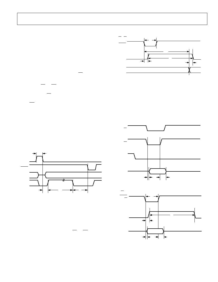
Figure 2. Load Circuit for Digital Interface Timing,
SDOUT, SYNC, and SCLK Outputs, C
L
= 10 pF
0.8V
2V
2V
0.8V
0.8V
2V
t
DELAY
t
DELAY
0
60
24-
0
03
Figure 3. Voltage Reference Levels for Timing
AD7643
Rev. 0 | Page 7 of 28
ABSOLUTE MAXIMUM RATINGS
Table 5.
Parameter Rating
Analog Inputs/Outputs
IN+
1
, IN-, REF, REFBUFIN, TEMP,
INGND, REFGND to AGND
AVDD + 0.3 V to
AGND - 0.3 V
Ground Voltage Differences
AGND, DGND, OGND
±0.3 V
Supply Voltages
AVDD, DVDD
-0.3 V to +2.7 V
OVDD
-0.3 V to +3.8 V
AVDD to DVDD
±2.8 V
AVDD, DVDD to OVDD
-3.8 V to +2.8 V
Digital Inputs
-0.3 V to +5.5 V
PDREF, PDBUF
2
±20 mA
Internal Power Dissipation
3
700 mW
Internal Power Dissipation
4
2.5 W
Junction Temperature
125°C
Storage Temperature Range
65°C to +125°C
1
See Analog Inputs section.
2
See Voltage Reference Input section.
3
Specification is for the device in free air:
48-Lead LQFP;
JA
= 91°C/W,
JC
= 30°C/W.
4
Specification is for the device in free air:
48-Lead LFCSP;
JA
= 26°C/W.
Stresses above those listed under Absolute Maximum Ratings
may cause permanent damage to the device. This is a stress
rating only; functional operation of the device at these or any
other conditions above those indicated in the operational
section of this specification is not implied. Exposure to absolute
maximum rating conditions for extended periods may affect
device reliability.
ESD CAUTION
ESD (electrostatic discharge) sensitive device. Electrostatic charges as high as 4000 V readily accumulate on
the human body and test equipment and can discharge without detection. Although this product features
proprietary ESD protection circuitry, permanent damage may occur on devices subjected to high energy
electrostatic discharges. Therefore, proper ESD precautions are recommended to avoid performance
degradation or loss of functionality.
AD7643
Rev. 0 | Page 8 of 28
PIN CONFIGURATION AND FUNCTION DESCRIPTIONS
36
35
34
33
32
31
30
29
28
27
26
25
13 14 15 16 17 18 19 20 21 22 23 24
1
2
3
4
5
6
7
8
9
10
11
12
48 47 46 45 44
39 38 37
43 42 41 40
PIN 1
IDENTIFIER
TOP VIEW
(Not to Scale)
AGND
CNVST
PD
RESET
CS
RD
DGND
AGND
AVDD
MODE0
MODE1
D0/OB/2C
NC = NO CONNECT
D1/A0
D2/A1
D3
D4/DIVSCLK[0]
BUSY
D17
D16
D15
AD7643
D5/DIVSCLK[1]
D14
D
6
/E
X
T
/IN
T
D7/
I
NV
S
Y
N
C
D
8
/IN
V
S
C
L
K
D
9
/R
D
C
/S
D
I
N
OGN
D
OV
D
D
DV
DD
DG
ND
D10
/
S
D
O
U
T
D1
1
/
S
C
L
K
D12
/
S
Y
NC
D
1
3/
RDE
RRO
R
P
DBUF
P
DRE
F
RE
F
BUF
I
N
TE
M
P
AV
D
D
IN
+
AG
ND
AG
ND
NC
IN
RE
F
G
ND
RE
F
06
02
4-
0
04
DGND
DGND
Figure 4. Pin Configuration
Table 6. Pin Function Descriptions
Pin
No.
Mnemonic Type
1
Description
1, 36,
41, 42
AGND
P
Analog Power Ground Pin.
2, 44
AVDD
P
Input Analog Power Pins. Nominally 2.5 V.
3, 4
MODE[0:1]
DI
Data Output Interface Mode Selection.
Interface MODE#
MODE1
MODE0
Description
0
0
0 18-bit
interface
1
0
1 16-bit
interface
2
1
0
8-bit (byte) interface
3
1
1 Serial
interface
5
D0/OB/2C
DI/O
When MODE[1:0] = 0 (18-bit interface mode), this pin is Bit 0 of the parallel port data output bus
and the data coding is straight binary. In all other modes, this pin allows the choice of straight
binary/twos complement. When OB/2C is high, the digital output is straight binary; when low,
the MSB is inverted resulting in a twos complement output from its internal shift register.
6, 7
DGND
P
Connect to Digital Ground.
8 D1/A0
DI/O
When MODE[1:0] = 0, this pin is Bit 1 of the parallel port data output bus. In all other modes, this
input pin controls the form in which data is output as shown in Table 7.
9
D2/A1
DI/O
When MODE[1:0] = 0, this pin is Bit 2 of the parallel port data output bus.
When MODE[1:0] = 1 or 2, this input pin controls the form in which data is output as shown in Table 7.
10 D3
DO When MODE[1:0] = 0, 1, or 2, this output is used as Bit 3 of the parallel port data output bus.
This pin is always an output, regardless of the interface mode.
11, 12
D[4:5]
DI/O
When MODE[1:0] = 0, 1, or 2, these pins are Bit 4 and Bit 5 of the parallel port data output bus.
or
DIVSCLK[0:1]
When MODE[1:0] = 3 (serial mode), serial clock division selection. When using serial master read
after convert mode (EXT/INT = low, RDC/SDIN = low), these inputs can be used to slow down the
internally generated serial clock that clocks the data output. In other serial modes, these pins are
high impedance outputs.
13
D6
DI/O
When MODE[1:0] = 0, 1, or 2, this output is used as Bit 6 of the parallel port data output bus.
or EXT/INT
When MODE[1:0] = 3 (serial mode), serial clock source select. This input is used to select the
internally generated (master) or external (slave) serial data clock.
When EXT/INT = low, master mode. The internal serial clock is selected on SCLK output.
When EXT/INT = high, slave mode. The output data is synchronized to an external clock signal,
gated by CS, connected to the SCLK input.
AD7643
Rev. 0 | Page 9 of 28
Pin
No. Mnemonic Type
1
Description
14
D7
DI/O
When MODE[1:0] = 0, 1, or 2, this output is used as Bit 7 of the parallel port data output bus.
or
INVSYNC
When MODE[1:0] = 3 (serial mode), invert sync select. In serial master mode (EXT/INT = low), this
input is used to select the active state of the SYNC signal.
When INVSYNC = low, SYNC is active high.
When INVSYNC = high, SYNC is active low.
15
D8
DI/O
When MODE[1:0] = 0, 1, or 2, this output is used as Bit 8 of the parallel port data output bus.
or
INVSCLK
When MODE[1:0] = 3 (serial mode), invert SCLK select. In all serial modes, this input is used to
invert the SCLK signal.
16
D9
DI/O
When MODE[1:0] = 0, 1, or 2, this output is used as bit 9 of the parallel port data output bus.
or
RDC
When MODE[1:0] = 3 (serial mode), read during convert. When using serial master mode
(EXT/INT = low), RDC is used to select the read mode.
When RDC = high, the previous conversion result is output on SDOUT during conversion and
the period of SCLK changes (see the Master Serial Interface section).
When RDC = low (read after convert), the current result can be output on SDOUT only when
the conversion is complete.
or
SDIN When MODE[1:0] = 3 (serial mode), serial data in. When using serial slave mode (EXT/INT = high),
SDIN could be used as a data input to daisy-chain the conversion results from two or more ADCs
onto a single SDOUT line. The digital data level on SDIN is output on SDOUT with a delay of 18 SCLK
periods after the initiation of the read sequence.
17
OGND
P
Input/Output Interface Digital Power Ground.
18 OVDD
P Input/Output Interface Digital Power. Nominally at the same supply as the supply of the
host interface (2.5 V or 3 V).
19
DVDD
P
Digital Power. Nominally at 2.5 V.
20
DGND
P
Digital Power Ground.
21
D10
DO
When MODE[1:0] = 0, 1, or 2, this output is used as Bit 10 of the parallel port data output bus.
or
SDOUT When MODE[1:0] = 3 (serial mode), serial data output. In serial mode, this pin is used as the serial
data output synchronized to SCLK. Conversion results are stored in an on-chip register. The AD7643
provides the conversion result, MSB first, from its internal shift register. The data format is
determined by the logic level of OB/2C.
In master mode, EXT/INT = low. SDOUT is valid on both edges of SCLK.
In slave mode, EXT/INT = high:
When INVSCLK = low, SDOUT is updated on SCLK rising edge and valid on the next falling edge.
When INVSCLK = high, SDOUT is updated on SCLK falling edge and valid on the next rising edge.
22
D11
DI/O
When MODE[1:0] = 0, 1, or 2, this output is used as Bit 11 of the parallel port data output bus.
or
SCLK When MODE[1:0] = 3 (serial mode), serial clock. In all serial modes, this pin is used as the serial
data clock input or output, depending upon the logic state of the EXT/INT pin. The active edge
where the data SDOUT is updated depends on the logic state of the INVSCLK pin.
23
D12
DO
When MODE[1:0] = 0, 1, or 2, this output is used as Bit 12 of the parallel port data output bus.
or
SYNC When MODE[1:0] = 3 (serial mode), frame synchronization. In serial master mode (EXT/INT= low),
this output is used as a digital output frame synchronization for use with the internal data clock.
When a read sequence is initiated and INVSYNC = low, SYNC is driven high and remains high
while SDOUT output is valid.
When a read sequence is initiated and INVSYNC = high, SYNC is driven low and remains low
while SDOUT output is valid.
24
D13
DO
When MODE[1:0] = 0, 1, or 2, this output is used as Bit 13 of the parallel port data output bus.
or
RDERROR
When MODE[1:0] = 3 (serial mode), read error. In serial slave mode (EXT/INT = high), this output
is used as an incomplete read error flag. If a data read is started and not completed when the
current conversion is complete, the current data is lost and RDERROR is pulsed high.
25 to
28
D[14:17] DO
Bit 14 to Bit 17 of the Parallel Port Data Output Bus. These pins are always outputs, regardless of
the interface mode.
29 BUSY
DO Busy Output. Transitions high when a conversion is started and remains high until the conversion
is complete and the data is latched into the on-chip shift register. The falling edge of BUSY can be
used as a data-ready clock signal.
30
DGND
P
Digital Power Ground.
AD7643
Rev. 0 | Page 10 of 28
Pin
No. Mnemonic Type
1
Description
31
RD
DI
Read Data. When CS and RD are both low, the interface parallel or serial output bus is enabled.
32
CS
DI
Chip Select. When CS and RD are both low, the interface parallel or serial output bus is enabled.
CS is also used to gate the external clock in slave serial mode.
33 RESET
DI Reset Input. When high, resets the AD7643. Current conversion, if any, is aborted. Falling edge of
RESET enables the calibration mode indicated by pulsing BUSY high. Refer to the Digital Interface
section. If not used, this pin can be tied to DGND.
34 PD
DI Power-Down Input. When high, powers down the ADC. Power consumption is reduced and
conversions are inhibited after the current one is completed.
35
CNVST
DI
Conversion Start. A falling edge on CNVST puts the internal sample-and-hold into the hold state
and initiates a conversion.
37
REF
AI/O
Reference Output/Input.
When PDREF/PDBUF = low, the internal reference and buffer are enabled producing 2.048 V on this pin.
When PDREF/PDBUF = high, the internal reference and buffer are disabled allowing an externally
supplied voltage reference up to AVDD volts. Decoupling is required with or without the internal
reference and buffer. Refer to the Voltage Reference Input section.
38
REFGND
AI
Reference Input Analog Ground.
39
IN-
AI
Differential Negative Analog Input.
40 NC
No
Connect.
43
IN+
AI
Differential Positive Analog Input.
45
TEMP
AO
Temperature Sensor Analog Output. Normally, 278 mV @ 25°C with a temperature coefficient
of 1 mV/°C. This pin can be used to measure the temperature of the AD7643. See the
Temperature Sensor section.
46
REFBUFIN
AI/O
Internal Reference Output/Reference Buffer Input.
When PDREF/PDBUF = low, the internal reference and buffer are enabled producing the 1.2 V (typical)
band gap output on this pin, which needs external decoupling. The internal fixed gain reference
buffer uses this to produce 2.048 V on the REF pin.
When using an external reference with the internal reference buffer (PDBUF = low, PDREF = high),
applying 1.2 V on this pin produces 2.048 V on the REF pin. Refer to the Voltage Reference Input section.
47
PDREF
DI
Internal Reference Power-Down Input.
When low, the internal reference is enabled.
When high, the internal reference is powered down and an external reference must been used.
48
PDBUF
DI
Internal Reference Buffer Power-Down Input.
When low, the buffer is enabled (must be low when using internal reference).
When high, the buffer is powered down.
1
AI = analog input; AI/O = bidirectional analog; AO = analog output; DI = digital input; DI/O = bidirectional digital; DO = digital output; P = power.
Table 7. Data Bus Interface Definition
MODE
MODE1
MODE0
D0/OB/2C
D1/A0
D2/A1 D[3] D[4:9] D[10:11] D[12:15] D[16:17] Description
0
0
0
R[0]
R[1]
R[2]
R[3]
R[4:9]
R[10:11]
R[12:15]
R[16:17]
18-Bit Parallel
1
0
1
OB/2C
A0 = 0
R[2]
R[3]
R[4:9]
R[10:11]
R[12:15]
R[16:17]
16-Bit High Word
1
0
1
OB/2C
A0 = 1
R[0]
R[1]
All Zeros
16-Bit Low Word
2
1
0
OB/2C
A0 = 0
A1 = 0
All Hi-Z
R[10:11]
R[12:15]
R[16:17]
8-Bit High Byte
2
1
0
OB/2C
A0 = 0
A1 = 1
All Hi-Z
R[2:3]
R[4:7]
R[8:9]
8-Bit Mid Byte
2
1
0
OB/2C
A0 = 1
A1 = 0
All Hi-Z
R[0:1]
All Zeros
8-Bit Low Byte
2
1
0
OB/2C
A0 = 1
A1 = 1
All Hi-Z
All Zeros
R[0:1]
8-Bit Low Byte
3
1
1
OB/2C
All Hi-Z
Serial Interface
Serial Interface

AD7643
Rev. 0 | Page 11 of 28
TERMINOLOGY
Integral Nonlinearity Error (INL)
Linearity error refers to the deviation of each individual code
from a line drawn from negative full scale through positive full
scale. The point used as negative full scale occurs ½ LSB before
the first code transition. Positive full scale is defined as a level
1½ LSB beyond the last code transition. The deviation is
measured from the middle of each code to the true straight line.
Differential Nonlinearity Error (DNL)
In an ideal ADC, code transitions are 1 LSB apart. Differential
nonlinearity is the maximum deviation from this ideal value. It
is often specified in terms of resolution for which no missing
codes are guaranteed.
Gain Error
The first transition (from 000...00 to 000...01) should occur for
an analog voltage ½ LSB above the nominal negative full scale
(-2.0479922 V for the ±2.048 V range). The last transition
(from 111...10 to 111...11) should occur for an analog voltage
1½ LSB below the nominal full scale (+2.0479766 V for the
±2.048 V range). The gain error is the deviation of the
difference between the actual level of the last transition and the
actual level of the first transition from the difference between
the ideal levels.
Zero Error
The zero error is the difference between the ideal midscale
input voltage (0 V) and the actual voltage producing the
midscale output code.
Dynamic Range
It is the ratio of the rms value of the full scale to the rms noise
measured with the inputs shorted together. The value for
dynamic range is expressed in decibels.
Signal-to-Noise Ratio (SNR)
SNR is the ratio of the rms value of the actual input signal to the
rms sum of all other spectral components below the Nyquist
frequency, excluding harmonics and dc. The value for SNR is
expressed in decibels.
Total Harmonic Distortion (THD)
THD is the ratio of the rms sum of the first five harmonic
components to the rms value of a full-scale input signal and is
expressed in decibels.
Signal to (Noise + Distortion) Ratio (SINAD)
SINAD is the ratio of the rms value of the actual input signal to
the rms sum of all other spectral components below the Nyquist
frequency, including harmonics but excluding dc. The value for
SINAD is expressed in decibels.
Spurious-Free Dynamic Range (SFDR)
The difference, in decibels (dB), between the rms amplitude of
the input signal and the peak spurious signal.
Effective Number of Bits (ENOB)
ENOB is a measurement of the resolution with a sine wave
input. It is related to SINAD and is expressed in bits by
ENOB = [(SINAD
dB
- 1.76)/6.02]
Aperture Delay
Aperture delay is a measure of the acquisition performance and
is measured from the falling edge of the CNVST input to when
the input signal is held for a conversion.
Transient Response
The time required for the AD7643 to achieve its rated accuracy
after a full-scale step function is applied to its input.
Reference Voltage Temperature Coefficient
It is derived from the typical shift of output voltage at 25°C on a
sample of parts maximum and minimum reference output
voltage (V
) measured at T
, T(25°C), and T
. It is
expressed in ppm/°C using
REF
MIN
MAX
(
)
(
)
(
)
(
)
(
)
6
10
C
25
C
ppm/
×
-
×
°
-
=
°
MIN
MAX
REF
REF
REF
REF
T
T
V
Min
V
Max
V
TCV
where:
V
REF
(Max) = Maximum V
REF
at T
MIN
, T(25°C), or T
MAX
V
REF
(Min) = Minimum V
REF
at T
MIN
, T(25°C), or T
MAX
V
REF
(25°C) = V
REF
at 25°C
T
MAX
= +85°C
T
MIN
= 40°C
AD7643
Rev. 0 | Page 12 of 28
TYPICAL PERFORMANCE CHARACTERISTICS
3.0
3.0
0
262144
CODE
IN
L
(
L
S
B
)
2.5
2.0
1.5
1.0
0.5
0
0.5
1.0
1.5
2.0
2.5
65536
131072
196608
06
02
4-
00
5
Figure 5. Integral Nonlinearity vs. Code
40000
0
1F
F
E
E
1
FFE
F
1F
F
F
0
1F
F
F
1
1F
F
F
2
1F
F
F
3
1F
F
F
4
1F
F
F
5
1F
F
F
6
1F
F
F
7
1F
F
F
8
1F
F
F
9
1F
F
F
A
1
F
FFB
1
F
FFC
1
F
FFD
1
FFF
E
1F
F
F
F
CODE IN HEX
CO
UNT
S
06
024
-
0
06
35000
30000
25000
20000
15000
10000
5000
= 1.67
V
REF
= 2.5V
0
1
3
16
3
0
228
59
33606
26875
23521
17320
4848
3062
13376
6371
1295
488
Figure 6. Histogram of 131,072 Conversions of a DC Input at
the Code Center (External Reference)
2.0486
2.0484
2.0482
2.0480
2.0478
2.0476
2.0474
2.0472
2.0470
55
125
105
85
65
45
25
5
15
35
TEMPERATURE (°C)
V
RE
F
(V
)
06
02
4-
0
07
Figure 7. Typical Reference Voltage Output vs. Temperature (2 Units)
1.25
1.0
0
262144
CODE
DN
L
(
L
S
B)
0.5
65536
131072
196608
1.0
0
0.5
06
02
4-
0
08
Figure 8. Differential Nonlinearity vs. Code
35000
0
2002
7
2002
8
2002
9
2002
A
20
02B
20
02C
20
02D
2002
E
20
02F
2003
0
2003
1
2003
2
2003
3
2003
4
2003
5
2003
6
2003
7
2003
8
CODE IN HEX
CO
UNT
S
06
024
-
0
09
30000
25000
20000
15000
10000
5000
21 28 305 665
297 108 3
2
4726 5401
15505
18613
28621
24350
16141
3807
10173
2306
= 2.04
V
REF
= 2.048V
Figure 9. Histogram of 131,072 Conversions of a DC Input at
the Code Center (Internal Reference)
12
12
10
8
6
4
2
0
2
4
6
8
10
55
125
105
85
65
45
25
5
15
35
TEMPERATURE (°C)
Z
E
R
O
E
R
RO
R
,
G
AI
N E
RRO
R (
L
S
B)
06
02
4-
0
10
GAIN ERROR
ZERO ERROR
Figure 10. Zero Error, Gain Error vs. Temperature
AD7643
Rev. 0 | Page 13 of 28
FREQUENCY (kHz)
A
M
P
L
ITU
D
E
(
d
B
of
Ful
l
S
c
a
l
e
)
0
180
0
600
0
180
0
600
FREQUENCY (kHz)
A
M
P
L
ITU
D
E
(
d
B
of
Ful
l
S
c
a
l
e
)
06
02
4-
01
1
20
40
60
80
100
120
140
160
100
200
300
400
500
f
S
= 1.25MSPS
f
IN
= 20.03kHz
SNR = 93.4dB
THD = 113dB
SFDR = 108dB
SINAD = 93.4dB
06
02
4-
01
4
20
40
60
80
100
120
140
160
100
200
300
400
500
f
S
= 1.25MSPS
f
IN
= 100.03kHz
SNR = 93dB
THD = 106dB
SFDR = 109dB
SINAD = 92.8dB
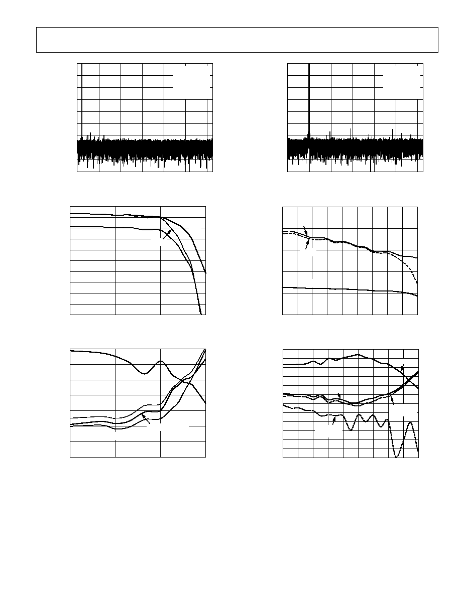
Figure 11. FFT 20 kHz
95
75
1
1000
FREQUENCY (kHz)
S
NR,
S
I
NAD
(
d
B)
SINAD
ENOB
SNR
06
02
4-
01
2
93
91
89
87
85
83
81
79
77
16.0
12.0
E
N
OB
(
B
it
s
)
15.6
15.2
14.8
14.4
14.0
13.6
13.2
12.8
12.4
10
100
Figure 12. SNR, SINAD, and ENOB vs. Frequency
70
140
1
1000
FREQUENCY (kHz)
T
HD,
HAR
M
O
NI
CS
(
d
B)
SFDR
THD
06
02
4-
01
3
120
20
S
F
DR (
d
B)
110
100
90
80
70
60
50
40
30
10
100
80
90
100
110
120
130
THIRD HARMONIC
SECOND HARMONIC
Figure 13. THD, Harmonics, and SFDR vs. Frequency
Figure 14. FFT 100 kHz
95
94
93
92
91
90
19
18
17
16
15
14
55
125
105
SNR
85
65
45
25
5
15
35
TEMPERATURE (°C)
S
NR,
S
I
NAD (
d
B)
EN
O
B
(B
i
t
s
)
06
02
4-
0
15
ENOB
SINAD
Figure 15. SNR, SINAD, and ENOB vs. Temperature
85
90
95
100
105
110
115
120
125
130
135
140
145
120
60
70
80
90
100
110
55
125
105
85
65
45
25
5
15
35
TEMPERATURE (°C)
T
HD,
HARM
O
NI
C
S
(
d
B)
S
F
DR (
d
B
)
06
02
4-
0
16
SFDR
THD
SECOND
HARMONIC
THIRD
HARMONIC
Figure 16. THD, Harmonics, and SFDR vs. Temperature
AD7643
Rev. 0 | Page 14 of 28
96.0
93.0
60
0
INPUT LEVEL (dB)
S
NR,
S
I
NAD
R
E
F
E
RRE
D T
O
F
U
L
L
S
CAL
E
(
d
B)
SINAD
SNR
06
02
4-
01
7
95.5
95.0
94.5
94.0
93.5
50
40
30
20
10
Figure 17. SNR and SINAD vs. Input Level (Referred to Full Scale)
16
0
125
55
TEMPERATURE (°C)
O
P
E
RAT
I
NG
CUR
RE
NT
S
(
µ
A
)
14
12
10
8
6
4
2
35
15
5
25
45
65
85
105
DVDD
OVDD, 3.3V
OVDD, 2.5V
AVDD
06
02
4-
018
Figure 18. Power-Down Operating Currents vs. Temperature
100k
0.01
10
10M
SAMPLING RATE (SPS)
O
P
E
RA
T
I
NG
CURR
E
NT
S
(
µ
A)
100
1k
10k
100k
1M
0.1
1
10
100
1k
10k
AVDD
DVDD
OVDD = 3.3V
OVDD = 2.5V
PDREF = PDBUF = HIGH
06
02
4-
01
9
Figure 19. Operating Current vs. Sampling Rate
20
4
0
C
L
(pF)
t
12
DE
L
A
Y
(
n
s)
18
16
14
12
10
8
6
50
100
150
200
OVDD = 2.5V @ 85°C
OVDD = 3.3V @ 85°C
OVDD = 3.3V @ 25°C
OVDD = 2.5V @ 25°C
06
02
4-
0
20
Figure 20. Typical Delay vs. Load Capacitance C
L
AD7643
Rev. 0 | Page 15 of 28
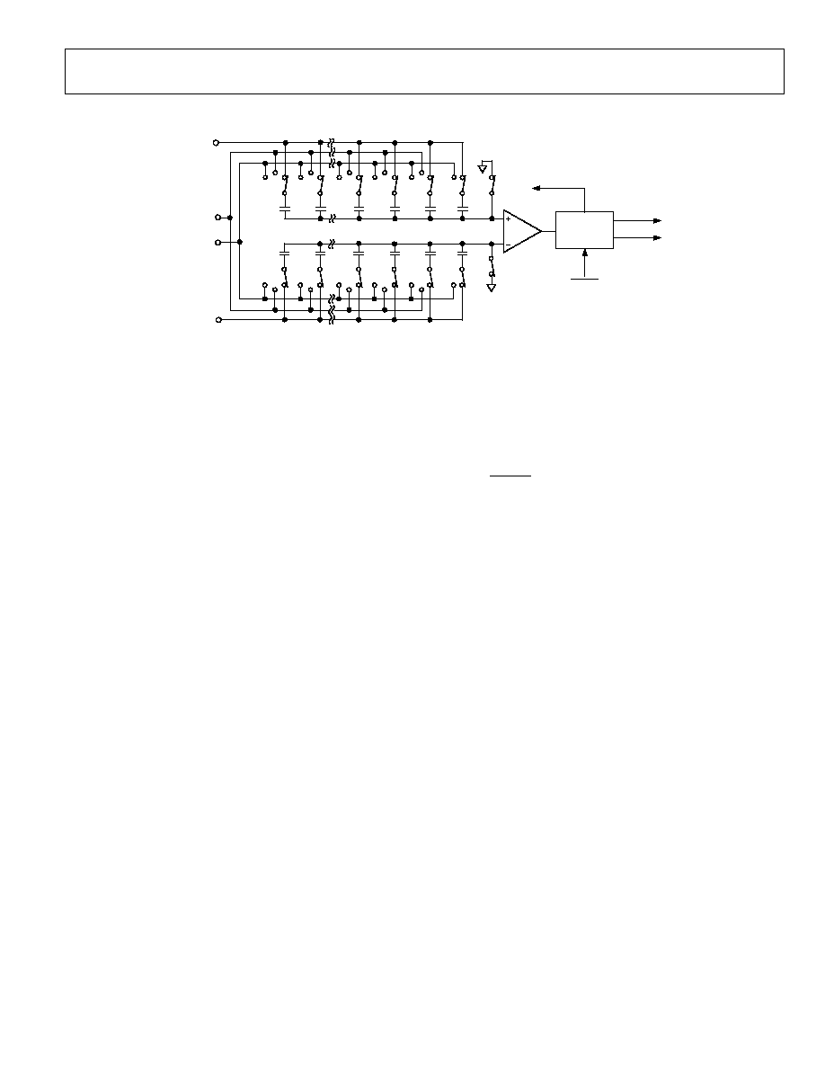
APPLICATIONS INFORMATION
SW+
COMP
SW
IN+
REF
REFGND
LSB
MSB
131,072C
65,536C
4C
2C
C
C
CONTROL
LOGIC
SWITCHES
CONTROL
BUSY
OUTPUT
CODE
CNVST
IN
4C
2C
C
C
LSB
MSB
AGND
AGND
131,072C 65,536C
0
602
4-
021
Figure 21. ADC Simplified Schematic
CIRCUIT INFORMATION
The AD7643 is a very fast, low power, single-supply, precise
18-bit ADC using successive approximation architecture. The
AD7643 is capable of converting 1,250,000 samples per second
(1.25 MSPS).
The AD7643 provides the user with an on-chip, track-and-hold,
successive approximation ADC that does not exhibit any
pipeline or latency, making it ideal for multiple multiplexed
channel applications.
The AD7643 can operate from a single 2.5 V supply and
interface to either 5 V, 3.3 V, or 2.5 V digital logic. It is housed
in a Pb-free, 48-lead LQFP package or a tiny 48-lead LFCSP
package, which combines space savings with flexibility and
allows the AD7643 to be configured as either a serial or a
parallel interface. The AD7643 is pin-to-pin compatible with
the
AD7641
and is a speed upgrade of the
AD7674
,
AD7678
,
and
AD7679
.
CONVERTER OPERATION
The AD7643 is a successive approximation ADC based on a
charge redistribution DAC. Figure 21 shows the simplified
schematic of the ADC. The capacitive DAC consists of two
identical arrays of 16 binary weighted capacitors that are
connected to the two comparator inputs.
During the acquisition phase, terminals of the array tied to the
comparator's input are connected to AGND via SW+ and SW-.
All independent switches are connected to the analog inputs.
Therefore, the capacitor arrays are used as sampling capacitors
and acquire the analog signal on the IN+ and IN- inputs. A
conversion phase is initiated once the acquisition phase is complete
and the CNVST input goes low. When the conversion phase
begins, SW+ and SW- are opened first. The two capacitor
arrays are then disconnected from the inputs and connected to
the REFGND input. Therefore, the differential voltage between
the inputs (IN+ and IN-) captured at the end of the acquisition
phase is applied to the comparator inputs, causing the
comparator to become unbalanced. By switching each element
of the capacitor array between REFGND and REF, the comparator
input varies by binary weighted voltage steps (V
REF
/2, V
REF
/4
throughV
REF
/262144). The control logic toggles these switches,
starting with the MSB first, to bring the comparator back into a
balanced condition. After the completion of this process, the
control logic generates the ADC output code and brings BUSY
output low.
AD7643
Rev. 0 | Page 16 of 28
TRANSFER FUNCTIONS
Using the OB/2C digital input, except in 18-bit interface mode,
the AD7643 offers two output codings: straight binary and twos
complement. The LSB size with V
REF
= 2.048 V is 2 × V
REF
/
262,144, which is 15.623 V. Refer to Figure 22 and Table 8 for
the ideal transfer characteristic.
000...000
000...001
000...010
111...101
111...110
111...111
ADC CO
DE
(
S
t
r
a
i
g
h
t
Bi
n
a
r
y
)
ANALOG INPUT
+FSR 1.5 LSB
+FSR 1 LSB
FSR + 1 LSB
FSR
FSR + 0.5 LSB
060
24
-
02
2
Figure 22. ADC Ideal Transfer Function
Table 8. Output Codes and Ideal Input Voltages
Digital Output Code (Hex)
Description
Analog Input
V
REF
= 2.048 V
Straight
Binary
Twos
Complement
FSR -1 LSB
+2.0479844 V
0x3FFFF
1
0x1FFFF
1
FSR - 2 LSB
+2.0479688 V
0x3FFFE
0x1FFFE
Midscale + 1 LSB
+15.625 V
0x20001
0x00001
Midscale
0 V
0x20000
0x00000
Midscale - 1 LSB
-15.625 V
0x1FFFF
0x3FFFF
-FSR + 1 LSB
-2.0479844 V
0x00001
0x20001
-FSR
-2.048 V
0x00000
2
0x20000
2
1
This is also the code for overrange analog input (V
IN+
- V
IN-
above
+V
REF
- V
REFGND
).
2
This is also the code for underrange analog input (V
IN+
- V
IN-
below
-V
REF
+ V
REFGND
).
RD
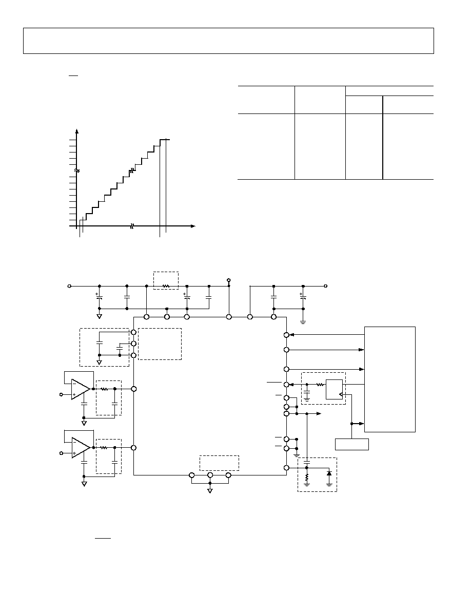
CS
100nF
100nF
AVDD
10µF
100nF
AGND
DGND
DVDD
OVDD
OGND
CNVST
BUSY
SDOUT
SCLK
RESET
PD
REFBUFIN
10
D
CLOCK
AD7643
MICROCONVERTER/
MICROPROCESSOR/
DSP
SERIAL
PORT
DIGITAL
INTERFACE
SUPPLY
(2.5V OR 3.3V)
ANALOG
SUPPLY (2.5V)
OVDD
DIGITAL
SUPPLY (2.5V)
IN+
IN
U2
15
NOTE 5
50
50pF
NOTE 1
ANALOG
INPUT +
C
C
C
C
2.7nF
2.7nF
U1
15
NOTE 1
MODE0
MODE1
D0/OB/2C
REFGND
REF
PDBUF
PDREF
100nF
ANALOG
INPUT
NOTE 2
NOTE 2
NOTE 3
NOTE 4
NOTE 3
NOTE 7
NOTE 6
10µF
10µF
C
REF
10µF
10k
50pF
1. SEE ANALOG INPUTS SECTION.
2. THE AD8021 IS RECOMMENDED. SEE DRIVER AMPLIFIER CHOICE SECTION.
3. THE CONFIGURATION SHOWN IS USING THE INTERNAL REFERENCE. SEE VOLTAGE REFERENCE INPUT SECTION.
4. A 10µF CERAMIC CAPACITOR (X5R, 1206 SIZE) IS RECOMMENDED (FOR EXAMPLE, PANASONIC ECJ3YB0J106M).
SEE VOLTAGE REFERENCE INPUT SECTION.
5. OPTION, SEE POWER SUPPLY SECTION.
6. OPTION, SEE POWER-UP SECTION.
7. OPTIONAL LOW JITTER CNVST, SEE CONVERSION CONTROL SECTION.
06
02
4-
0
23
Figure 23. Typical Connection Diagram
AD7643
Rev. 0 | Page 17 of 28
TYPICAL CONNECTION DIAGRAM
Figure 23 shows a typical connection diagram for the AD7643.
Different circuitry shown in this diagram is optional and is
discussed in the following sections.
ANALOG INPUTS
Figure 24 shows an equivalent circuit of the input structure of
the AD7643.
The two diodes, D
1
and D
2
, provide ESD protection for the
analog inputs IN+ and IN-. Care must be taken to ensure that
the analog input signal never exceeds the supply rails by more
than 0.3 V, because this causes the diodes to become forward-
biased and to start conducting current. These diodes can handle
a forward-biased current of 100 mA maximum. For instance,
these conditions could eventually occur when the input buffer's
U1 or U2 supplies are different from AVDD. In such a case, an
input buffer with a short-circuit current limitation can be used
to protect the part.
D
1
R
IN
C
IN
D
2
IN+ OR IN
AGND
AVDD
C
PIN
06
02
4-
02
4
Figure 24. AD7643 Simplified Analog Input
The analog input of the AD7643 is a true differential structure.
By using this differential input, small signals common to both
inputs are rejected, as shown in Figure 25, representing the
typical CMRR over frequency with internal and external references.
65
45
1
10000
FREQUENCY (kHz)
CM
R
R (
d
B)
10
100
1000
60
55
50
INT REF
EXT REF
06
02
4-
02
5
Figure 25. Analog Input CMRR vs. Frequency
During the acquisition phase for ac signals, the impedance of
the analog inputs, IN+ and IN-, can be modeled as a parallel
combination of capacitor C
PIN
and the network formed by the
series connection of R
IN
and C
IN
. C
PIN
is primarily the pin
capacitance. R
IN
is typically 175 and is a lumped component
comprised of some serial resistors and the on resistance of the
switches. C
IN
is typically 12 pF and is mainly the ADC sampling
capacitor. During the conversion phase, when the switches are
opened, the input impedance is limited to C
PIN
. R
IN
and C
IN
make a 1-pole, low-pass filter that has a typical -3 dB cutoff
frequency of 50 MHz, thereby reducing an undesirable aliasing
effect and limiting the noise coming from the inputs.
Because the input impedance of the AD7643 is very high, the
AD7643 can be driven directly by a low impedance source
without gain error. To further improve the noise filtering achieved
by the AD7643's analog input circuit, an external 1-pole RC
filter between the amplifier's outputs and the ADC analog
inputs can be used, as shown in Figure 23. However, large source
impedances significantly affect the ac performance, especially
the total harmonic distortion (THD). The maximum source
impedance depends on the amount of THD that can be
tolerated. The THD degrades as a function of the source
impedance and the maximum input frequency, as shown in
Figure 26.
70
110
1
10
100
1000
INPUT FREQUENCY (kHz)
T
HD (
d
B)
R
S
= 500
R
S
= 100
R
S
= 10
R
S
= 50
06
02
4-
02
6
75
80
85
90
95
100
105
Figure 26. THD vs. Analog Input Frequency and Source Resistance
MULTIPLEXED INPUTS
When using the full 1.25 MSPS throughput in multiplexed
applications for a full-scale step, the RC filter, as shown in
Figure 23, does not settle in the required acquisition time, t
8
.
These values are chosen to optimize the best SNR performance
of the AD7643. To use the full 1.25 MSPS throughput in
multiplexed applications, the RC should be adjusted to satisfy t
8
(which is ~ 8.5 × RC time constant). However, lowering R and C
increases the RC filter bandwidth and allows more noise into the
AD7643, which degrades SNR. To preserve the SNR performance
in these applications using the RC filter shown in Figure 23,
the AD7643 should be run with t
8
> 350 ns; or approximately
1/(t
7
+ t
8
) ~ 1.12 MSPS.
AD7643
Rev. 0 | Page 18 of 28
DRIVER AMPLIFIER CHOICE
Although the AD7643 is easy to drive, the driver amplifier
needs to meet the following requirements:
·
For multichannel, multiplexed applications, the driver
amplifier and the AD7643 analog input circuit must be
able to settle for a full-scale step of the capacitor array at an
18-bit level (0.0004%). In the amplifier's data sheet, settling
at 0.1% to 0.01% is more commonly specified. This could
differ significantly from the settling time at an 18-bit level
and should be verified prior to driver selection. The
AD8021
op amp, which combines ultralow noise and high
gain bandwidth, meets this settling time requirement even
when used with gains up to 13.
·
The noise generated by the driver amplifier needs to be
kept as low as possible to preserve the SNR and transition
noise performance of the AD7643. The noise coming from
the driver is filtered by the AD7643 analog input circuit
1-pole, low-pass filter made by R
IN
and C
IN
or by the
external filter, if one is used. The SNR degradation due
to the amplifier is
(
)
(
)
+
+
=
-
-
+
-
2
2
2
2
900
30
20log
N
3dB
N
3dB
LOSS
Ne
f
Ne
f
SNR
where:
f
3dB
is the input bandwidth of the AD7643 (50 MHz) or
the cutoff frequency of the input RC filter shown in Figure 23
(3.9 MHz), if one is used.
N is the noise factor of the amplifier (1 in buffer
configuration).
e
N+
and e
N-
are the equivalent input voltage noise densities
of the op amps connected to IN+ and IN-, in nV/Hz.
This approximation can be used when the resistances used
around the amplifier are small. If larger resistances are
used, their noise contributions should also be root-sum
squared.
For instance, when using op amps with an equivalent input
noise density of 2.1 nV/Hz, such as the
AD8021
, with a
noise gain of 1 when configured as a buffer, degrades the
SNR by only 0.25 dB when using the RC filter in Figure 23,
and by 2.5 dB without it.
·
The driver needs to have a THD performance suitable to
that of the AD7643. Figure 13 gives the THD vs. frequency
that the driver should exceed.
The
AD8021
meets these requirements and is appropriate for
almost all applications. The
AD8021
needs a 10 pF external
compensation capacitor that should have good linearity as an
NPO ceramic or mica type. Moreover, the use of a noninverting
1 gain arrangement is recommended and helps to obtain the
best signal-to-noise ratio.
The
AD8022
can also be used when a dual version is needed
and a gain of 1 is present. The
AD829
is an alternative in
applications where high frequency (above 100 kHz) performance is
not required. In applications with a gain of 1, an 82 pF
compensation capacitor is required. The
AD8610
is an option
when low bias current is needed in low frequency applications.
Single-to-Differential Driver
For applications using unipolar analog signals, a single-ended-
to-differential driver, as shown in Figure 27, allows for a
differential input into the part. This configuration, when
provided an input signal of 0 to V
REF
, produces a differential
±V
REF
with midscale at V
REF
/2. The 1-pole filter using R = 15
and C = 2.7 nF provides a corner frequency of 3.9 MHz.
If the application can tolerate more noise, the
AD8139
differential driver can be used.
AD8021
ANALOG INPUT
(UNIPOLAR 0V TO 2.048V)
AD8021
IN+
IN
AD7643
REF
10µF
15
15
100nF
2.7nF
2.7nF
U2
U1
10pF
10pF
5k
5k
590
590
0
602
4-
027
Figure 27. Single-Ended-to-Differential Driver Circuit
(Internal Reference Buffer Used)
VOLTAGE REFERENCE INPUT
The AD7643 allows the choice of either a very low temperature
drift internal voltage reference, an external 1.2 V reference that
can be buffered using the internal reference buffer, or an
external reference.
Unlike many ADCs with internal references, the internal
reference of the AD7643 provides excellent performance and
can be used in almost all applications.
AD7643
Rev. 0 | Page 19 of 28
Internal Reference (PDBUF = Low, PDREF = Low)
To use the internal reference, the PDREF and PDBUF inputs
must both be low. This produces a 1.2 V band gap output on
REFBUFIN, which is amplified by the internal buffer and
results in a 2.048 V reference on the REF pin.
The internal reference is temperature compensated to 2.048 V ±
10 mV. The reference is trimmed to provide a typical drift of
8 ppm/°C. This typical drift characteristic is shown in Figure 7.
The output resistance of REFBUFIN is 6.33 k (minimum)
when the internal reference is enabled. It is necessary to
decouple this with a ceramic capacitor greater than 100 nF.
Therefore, the capacitor provides an RC filter for noise reduction.
Because the output impedance of REFBUFIN is typically
6.33 k, relative humidity (among other industrial contaminates)
can directly affect the drift characteristics of the reference.
Typically, a guard ring is used to reduce the effects of drift
under such circumstances. However, because the AD7643 has a
fine lead pitch, guarding this node is not practical. Therefore, in
these industrial and other types of applications, it is recommended
to use a conformal coating, such as Dow Corning® 1-2577 or
HumiSeal® 1B73.
External 1.2 V Reference and Internal Buffer (PDBUF =
Low, PDREF = High)
To use an external reference along with the internal buffer,
PDREF should be high and PDBUF should be low. This powers
down the internal reference and allows an external 1.2 V
reference to be applied to REFBUFIN, producing 2.048 V
(typically) on the REF pin.
External 2.5 V Reference (PDBUF = High, PDREF = High)
To use an external 2.5 V reference directly on the REF pin,
PDREF and PDBUF should both be high.
For improved drift performance, an external reference, such as
the
AD780
or
ADR431
, can be used. The advantages of directly
using the external voltage reference are:
·
The SNR and dynamic range improvement (about 1.7 dB)
resulting from the use of a reference voltage very close to
the supply (2.5 V) instead of a typical 2.048 V reference
when the internal reference is used. This is calculated by
=
50
.
2
048
.
2
log
20
SNR
·
The power savings when the internal reference is powered
down (PDREF high).
PDREF and PDBUF power down the internal reference and
the internal reference buffer, respectively. The input current
of PDREF and PDBUF should never exceed 20 mA. This can
occur when the driving voltage is above AVDD (for instance, at
power-up). In this case, a 125 series resistor is recommended.
Reference Decoupling
Whether using an internal or external reference, the AD7643
voltage reference input (REF) has a dynamic input impedance;
therefore, it should be driven by a low impedance source with
efficient decoupling between the REF and REFGND inputs.
This decoupling depends on the choice of the voltage reference
but usually consists of a low ESR capacitor connected to REF
and REFGND with minimum parasitic inductance.
A 10 F (X5R, 1206 size) ceramic chip capacitor (or 47 F
tantalum capacitor) is appropriate when using either the
internal reference or one of the recommended reference voltages.
The placement of the reference decoupling is also important to
the performance of the AD7643. The decoupling capacitor
should be mounted on the same side as the ADC right at the
REF pin with a thick PCB trace. The REFGND should also connect
to the reference decoupling capacitor with the shortest distance.
For applications that use multiple AD7643 devices, it is more
effective to use an external reference with the internal reference
buffer to buffer the reference voltage. However, because the
reference buffers are not unity gain, ratiometric, simultaneously
sampled designs should use an external reference and external
buffer, such as the
AD8031
/
AD8032
; therefore, preserving the
same reference level for all converters.
The voltage reference temperature coefficient (TC) directly
impacts full scale; therefore, in applications where full-scale
accuracy matters, care must be taken with the TC. For instance,
a ±4 ppm/°C TC of the reference changes full scale by ±1 LSB/°C.
Note that V
REF
can be increased to AVDD + 0.1 V. Because the
input range is defined in terms of V
REF
, this would essentially
increase the range to 0 V to 2.8 V with an AVDD = 2.7 V.
Temperature Sensor
The TEMP pin measures the temperature of the AD7643. To
improve the calibration accuracy over the temperature range,
the output of the TEMP pin is applied to one of the inputs of
the analog switch (such as,
ADG779
), and the ADC itself is
used to measure its own temperature. This configuration is
shown in Figure 28.
ADG779
AD8021
C
C
ANALOG INPUT
(UNIPOLAR)
AD7643
IN+
TEMPERATURE
SENSOR
TEMP
06
02
4-
0
2
8
Figure 28. Use of the Temperature Sensor
AD7643
Rev. 0 | Page 20 of 28
POWER SUPPLY
The AD7643 uses three sets of power supply pins: an analog
2.5 V supply AVDD, a digital 2.5 V core supply DVDD, and a
digital input/output interface supply OVDD. The OVDD supply
allows direct interface with any logic working between 2.3 V
and 5.25 V. To reduce the number of supplies needed, the digital
core (DVDD) can be supplied through a simple RC filter from
the analog supply, as shown in Figure 23.
Power Sequencing
The AD7643 is independent of power supply sequencing and
thus free from supply induced voltage latch-up. In addition, it is
insensitive to power supply variations over a wide frequency
range, as shown in Figure 29.
65.0
45.0
1
10000
FREQUENCY (kHz)
PS
R
R
(d
B
)
10
100
1000
62.5
60.0
57.5
55.0
52.5
50.0
47.5
INT REF
EXT REF
06
02
4-
02
9
Figure 29. PSRR vs. Frequency
Power-Up
At power-up, or when returning to operational mode from the
power-down mode (PD = high), the AD7643 engages an
initialization process. During this time, the first 128 conversions
should be ignored or the RESET input could be pulsed to
engage a faster initialization process. Refer to the Digital
Interface section for RESET and timing details.
A simple power-on reset circuit, as shown in Figure 23, can be
used to minimize the digital interface. As OVDD powers up, the
capacitor is shorted and brings RESET high; it is then charged
returning RESET to low. However, this circuit only works when
powering up the AD7643 because the power-down mode
(PD = high) does not power down any of the supplies and as a
result, RESET is low.
It should be noted that the digital interface remains active even
during the acquisition phase. To reduce the operating digital
supply currents even further, drive the digital inputs close to
the power rails (that is, OVDD and OGND).
CONVERSION CONTROL
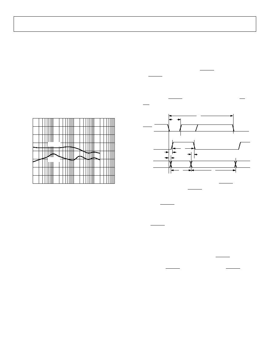
The AD7643 is controlled by the CNVST input. A falling edge
on CNVST is all that is necessary to initiate a conversion.
Detailed timing diagrams of the conversion process are shown
in Figure 30. Once initiated, it cannot be restarted or aborted,
even by the power-down input, PD, until the conversion is
complete. The CNVST signal operates independently of CS and
RD signals.
BUSY
MODE
CONVERT
ACQUIRE
ACQUIRE
CONVERT
CNVST
t
1
t
2
t
4
t
3
t
5
t
6
t
7
t
8
06
02
4-
0
30
Figure 30. Basic Conversion Timing
For optimal performance, the rising edge of CNVST should not
occur after the maximum CNVST low time, t
1
, or until the end
of conversion.
Although CNVST is a digital signal, it should be designed with
special care with fast, clean edges and levels with minimum
overshoot and undershoot or ringing.
The CNVST trace should be shielded with ground and a low
value serial resistor (for example, 50 ) termination should be
added close to the output of the component that drives this line.
In addition, a 50 pF capacitor is recommended to further reduce
the effects of overshoot and undershoot as shown in Figure 23.
For applications where SNR is critical, the CNVST signal should
have very low jitter. This can be achieved by using a dedicated
oscillator for CNVST generation, or by clocking CNVST with a
high frequency, low jitter clock, as shown in Figure 23.
AD7643
Rev. 0 | Page 21 of 28
INTERFACES
DIGITAL INTERFACE
The AD7643 has a versatile digital interface that can be set up
as either a serial or a parallel interface with the host system. The
serial interface is multiplexed on the parallel data bus. The AD7643
digital interface also accommodates 2.5 V, 3.3 V, or 5 V logic
with either OVDD at 2.5 V or 3.3 V. OVDD defines the logic
high output voltage. In most applications, the OVDD supply pin
of the AD7643 is connected to the host system interface 2.5 V
or 3.3 V digital supply. By using the D0/OB/2C input pin, either
twos complement or straight binary coding can be used.
The two signals CS and RD control the interface. When at least
one of these signals is high, the interface outputs are in high
impedance. Usually, CS allows the selection of each AD7643 in
multicircuit applications and is held low in a single AD7643
design. RD is generally used to enable the conversion result on
the data bus.
RESET
The RESET input is used to reset the AD7643 and generate a
fast initialization. A rising edge on RESET aborts the current
conversion (if any) and tristates the data bus. The falling edge of
RESET clears the data bus and engages the initialization process
indicated by pulsing BUSY high. Conversions can take place
after the falling edge of BUSY. Refer to Figure 31 for the RESET
timing details.
RESET
DATA
BUSY
CNVST
t
38
t
39
t
8
t
9
06
02
4-
0
31
Figure 31. RESET Timing
PARALLEL INTERFACE
The AD7643 is configured to use the parallel interface for an
18-bit, 16-bit, or 8-bit bus width according to Table 7.
Master Parallel Interface
Data can be continuously read by tying CS and RD low, thus
requiring minimal microprocessor connections. However, in
this mode, the data bus is always driven and cannot be used in
shared bus applications, unless the device is held in RESET.
Figure 32 details the timing for this mode.
t
1
BUSY
DATA
BUS
PREVIOUS CONVERSION DATA
NEW DATA
CNVST
CS = RD = 0
t
10
t
4
t
11
t
3
06
024-
032
Figure 32. Master Parallel Data Timing for Reading (Continuous Read)
Slave Parallel Interface
In slave parallel reading mode, the data can be read either after
each conversion, which is during the next acquisition phase, or
during the following conversion, as shown in Figure 33 and
Figure 34, respectively. When the data is read during the
conversion, it is recommended that it is read-only during the
first half of the conversion phase. This avoids any potential
feedthrough between voltage transients on the digital interface
and the most critical analog conversion circuitry.
CURRENT
CONVERSION
t
13
t
12
BUSY
DATA
BUS
RD
CS
060
24
-
03
3
Figure 33. Slave Parallel Data Timing for Reading (Read After Convert)
PREVIOUS
CONVERSION
t
13
t
12
t
3
BUSY
DATA
BUS
CNVST,
RD
CS = 0
t
4
t
1
060
24
-
03
4
Figure 34. Slave Parallel Data Timing for Reading (Read During Convert)
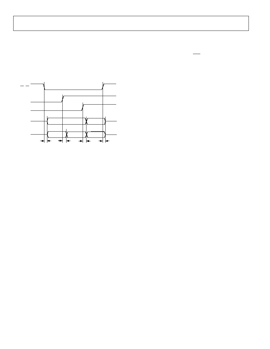
AD7643
Rev. 0 | Page 22 of 28
16-Bit and 8-Bit Interface (Master or Slave)
In the 16-bit (MODE[1:0] = 1) and 8-bit (MODE[1:0] = 2)
interfaces, the A0/A1 pins allow a glueless interface to a 16- or
8-bit bus, as shown in Figure 35. By connecting A0/A1 to an
address line(s), the data can be read in two words for a 16-bit
interface, or three bytes for an 8-bit interface. This interface can
be used in both master and slave parallel reading modes. Refer
to Table 7 for the full details of the interface.
CS, RD
A1
D[17:2]
HI-Z
HIGH
WORD
LOW
WORD
HI-Z
t
12
t
13
HIGH
BYTE
A0
MID
BYTE
LOW
BYTE
D[17:10]
t
12
HI-Z
HI-Z
t
12
06
02
4-
0
35
Figure 35. 8-Bit and 16-Bit Parallel Interface
SERIAL INTERFACE
The AD7643 is configured to use the serial interface when
MODE[1:0] = 3. The AD7643 outputs 18 bits of data, MSB first,
on the SDOUT pin. This data is synchronized with the 18 clock
pulses provided on the SCLK pin. The output data is valid on
both the rising and falling edge of the data clock.
MASTER SERIAL INTERFACE
Internal Clock
The AD7643 is configured to generate and provide the serial
data clock SCLK when the EXT/INT pin is held low. The
AD7643 also generates a SYNC signal to indicate to the host
when the serial data is valid. The serial clock SCLK and the
SYNC signal can be inverted. Depending on the read during
convert input, RDC/SDIN, the data can be read after each
conversion or during the following conversion. Figure 36 and
Figure 37 show detailed timing diagrams of these two modes.
Usually, because the AD7643 is used with a fast throughput, the
master read during conversion mode is the most recommended
serial mode. In this mode, the serial clock and data toggle at
appropriate instants, minimizing potential feedthrough between
digital activity and critical conversion decisions. In this mode,
the SCLK period changes because the LSBs require more time
to settle and the SCLK is derived from the SAR conversion cycle.
In read after conversion mode, it should be noted that unlike
other modes, the BUSY signal returns low after the 18 data bits
are pulsed out and not at the end of the conversion phase,
resulting in a longer BUSY width. As a result, the maximum
throughput cannot be achieved in this mode.
In addition, in read after convert mode, the SCLK frequency
can be slowed down to accommodate different hosts using the
DIVSCLK[1:0] inputs. Refer to Table 4 for the SCLK timing
details when using these inputs.
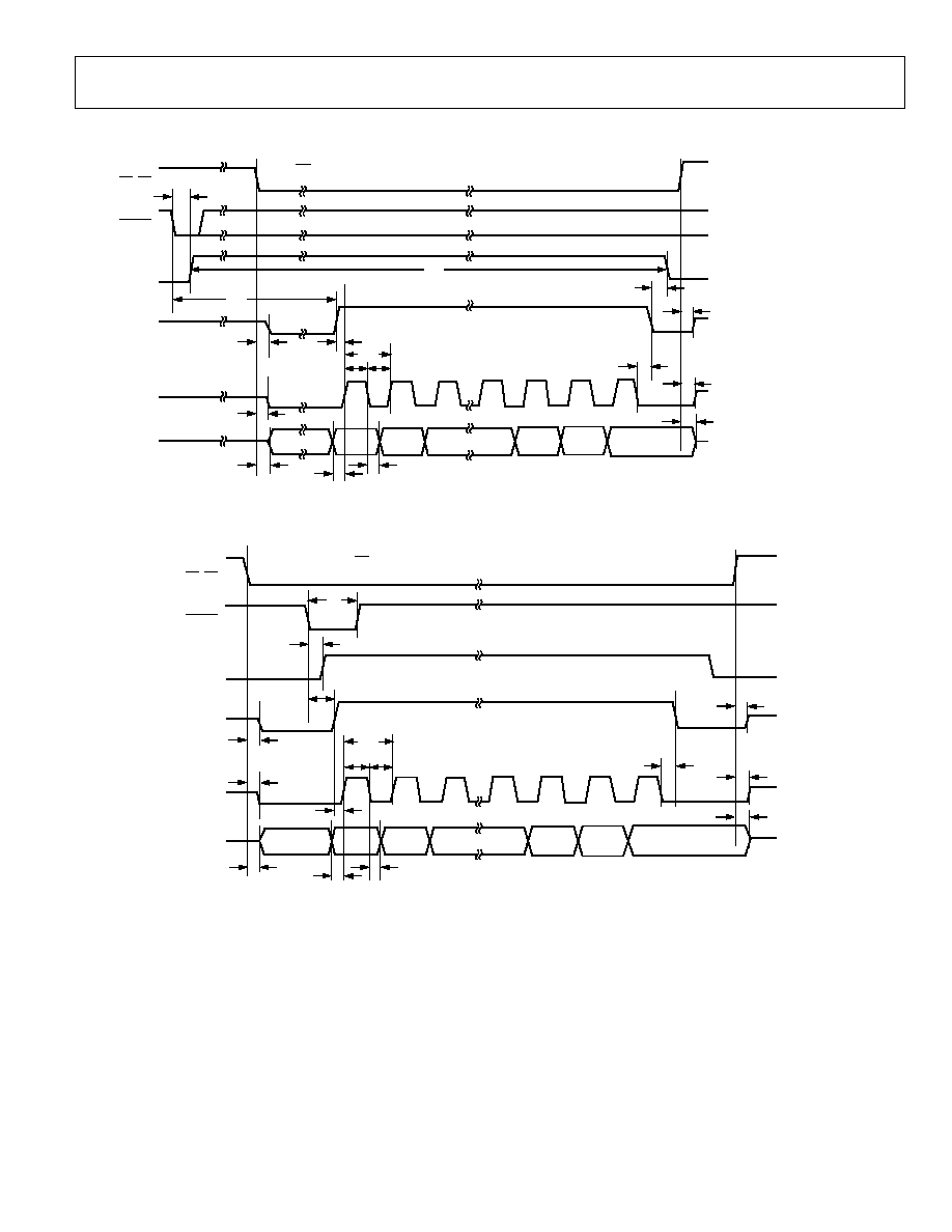
AD7643
Rev. 0 | Page 23 of 28
BUSY
SYNC
SCLK
SDOUT
1
2
3
16
17
18
D17
D16
D2
D1
D0
X
RDC/SDIN = 0
INVSCLK = INVSYNC = 0
CNVST
CS, RD
EXT/INT = 0
t
23
t
22
t
16
t
15
t
14
t
29
t
19
t
21
t
20
t
18
t
28
t
30
t
24
t
25
t
26
t
27
t
3
DIVSCLK[1:0] = 0
06
024
-
0
36
Figure 36. Master Serial Data Timing for Reading (Read After Convert)
EXT/INT = 0
RDC/SDIN = 1
INVSCLK = INVSYNC = 0
D17
D16
D2
D1
D0
X
1
2
3
16
17
18
BUSY
SYNC
SCLK
SDOUT
CNVST
CS, RD
t
23
t
18
t
15
t
14
t
17
t
3
t
22
t
16
t
1
t
25
t
26
t
24
t
27
t
19
t
20
t
21
0
60
24
-
03
7
Figure 37. Master Serial Data Timing for Reading (Read Previous Conversion During Convert)
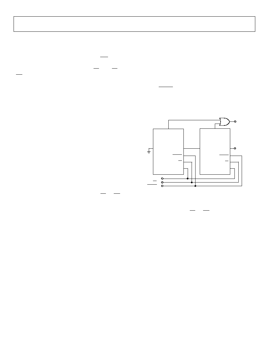
AD7643
Rev. 0 | Page 24 of 28
SLAVE SERIAL INTERFACE
External Clock
The AD7643 is configured to accept an externally supplied
serial data clock on the SCLK pin when the EXT/INT pin is
held high. In this mode, several methods can be used to read
the data. The external serial clock is gated by CS. When CS and
RD are both low, the data can be read after each conversion or
during the following conversion. The external clock can be
either a continuous or a discontinuous clock. A discontinuous
clock can be either normally high or normally low when
inactive. Figure 39 and Figure 40 show the detailed timing
diagrams of these methods.
While the AD7643 is performing a bit decision, it is important
that voltage transients be avoided on digital input/output pins
or degradation of the conversion result could occur. This is
particularly important during the second half of the conversion
phase because the AD7643 provides error correction circuitry
that can correct for an improper bit decision made during
the first half of the conversion phase. For this reason, it is
recommended that when an external clock is being provided,
a discontinuous clock is toggled only when BUSY is low or,
more importantly, that it does not transition during the latter
half of BUSY high.
External Discontinuous Clock Data Read After Conversion
Figure 39 shows the detailed timing diagrams of this method.
After a conversion is complete, indicated by BUSY returning
low, the conversion result can be read while both CS and RD are
low. Data is shifted out MSB first with 18 clock pulses and is
valid on the rising and falling edges of the clock.
Among the advantages of this method is the fact that conversion
performance is not degraded because there are no voltage
transients on the digital interface during the conversion process.
Another advantage is the ability to read the data at any speed up
to 80 MHz, which accommodates both the slow digital host
interface and the fast serial reading.
It is also possible to begin to read data after conversion and
continue to read the last bits after a new conversion is initiated.
In this reading mode, it is recommended to pause digital
activity just prior to initiating a conversion (SCLK should be
held high or low). Once the conversion has begun, the reading
can continue. Also, in this mode, the use of a slower clock speed
can be used to read the data because the total reading time is the
acquisition time, t
8
+ half of the conversion time, t
7
(t
8
+ ½ × t
7
, see
the External Clock Data Read During Previous Conversion
section).
Finally, in this mode only, the AD7643 provides a daisy-chain
feature using the RDC/SDIN pin for cascading multiple converters
together. This feature is useful for reducing component count
and wiring connections when desired, as, for instance, in
isolated multiconverter applications.
An example of the concatenation of two devices is shown in
Figure 38. Simultaneous sampling is possible by using a
common CNVST signal. It should be noted that the RDC/SDIN
input is latched on the edge of SCLK opposite to the one used to
shift out the data on SDOUT. Therefore, the MSB of the
upstream converter just follows the LSB of the downstream
converter on the next SCLK cycle.
SCLK
SDOUT
RDC/SDIN
AD7643
#1
(DOWNSTREAM)
AD7643
#2
(UPSTREAM)
BUSY
OUT
BUSY
BUSY
DATA
OUT
SCLK
RDC/SDIN
SDOUT
SCLK IN
CNVST IN
CNVST
CS
CNVST
CS
CS IN
06
02
4-
03
8
Figure 38. Two AD7643 Devices in a Daisy-Chain Configuration
External Clock Data Read During Previous Conversion
Figure 40 shows the detailed timing diagrams of this method.
During a conversion, while CS and RD are both low, the result
of the previous conversion can be read. The data is shifted out,
MSB first, with 18 clock pulses and is valid on both the rising
and falling edge of the clock. The 18 bits have to be read before
the current conversion is complete; otherwise, RDERROR is
pulsed high and can be used to interrupt the host interface to
prevent incomplete data reading. There is no daisy-chain
feature in this mode, and the RDC/SDIN input should always
be tied either high or low.
To reduce performance degradation due to digital activity, a fast
discontinuous clock of at least 67 MHz is recommended to
ensure that all the bits are read during the first half of the SAR
conversion phase, t
7
, because the ADC can correct for errors
introduced by digital activity during this time.
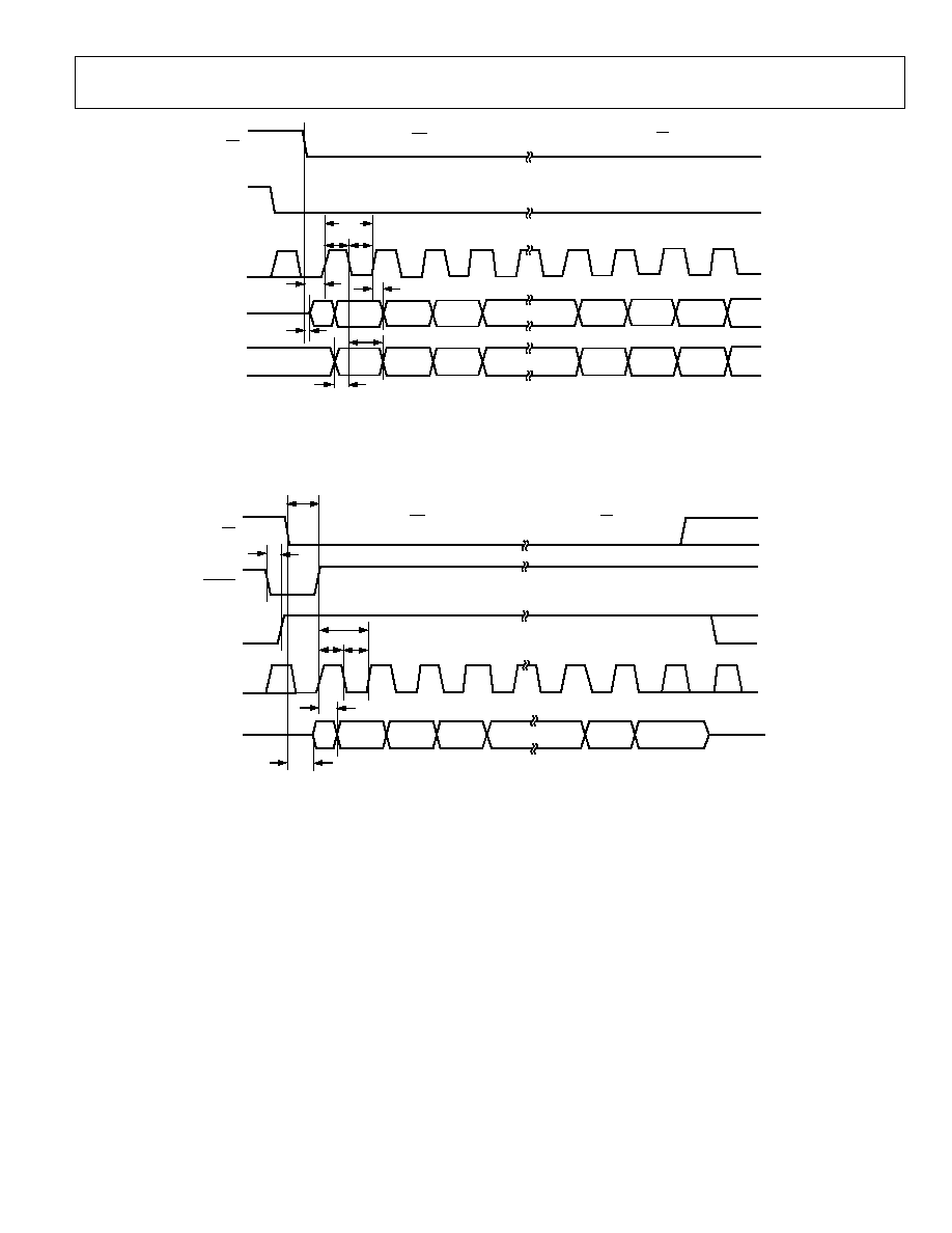
AD7643
Rev. 0 | Page 25 of 28
SCLK
SDOUT
D17
D16
D1
D0
D15
X17
X16
X15
X1
X0
Y17
Y16
BUSY
SDIN
INVSCLK = 0
X17
X16
X
1
2
3
16
17
18
19
20
EXT/INT = 1
CS
RD = 0
t
33
t
16
t
34
t
31
t
32
t
35
t
36
t
37
060
24
-
0
39
Figure 39. Slave Serial Data Timing for Reading (Read After Convert)
SDOUT
SCLK
D1
D0
X
D17
D16
D15
1
2
3
17
18
BUSY
EXT/INT = 1
INVSCLK = 0
CNVST
CS
RD = 0
t
16
t
31
t
32
t
35
t
3
t
36
t
37
4
D2
16
0
60
24
-
04
0
Figure 40. Slave Serial Data Timing for Reading (Read Previous Conversion During Convert)
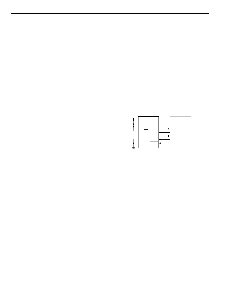
AD7643
Rev. 0 | Page 26 of 28
MICROPROCESSOR INTERFACING
The AD7643 is ideally suited for traditional dc measurement
applications supporting a microprocessor, and ac signal processing
applications interfacing to a digital signal processor. The
AD7643 is designed to interface with a parallel 8-bit or 16-bit
wide interface or with a general-purpose serial port or I/O ports
on a microcontroller. A variety of external buffers can be used
with the AD7643 to prevent digital noise from coupling into the
ADC. The SPI Interface (ADSP-219x) section illustrates the use
of the AD7643 with the ADSP-219x SPI-equipped DSP.
SPI Interface (ADSP-219x)
Figure 41 shows an interface diagram between the AD7643 and
an SPI-equipped DSP, the ADSP-219x. To accommodate the
slower speed of the DSP, the AD7643 acts as a slave device and
data must be read after conversion. This mode also allows the
daisy-chain feature. The convert command can be initiated in
response to an internal timer interrupt. The 18-bit output data
are read with three SPI byte access. The reading process can be
initiated in response to the end-of-conversion signal (BUSY
going low) using an interrupt line of the DSP. The serial
peripheral interface (SPI) on the ADSP-219x is configured for
master mode (MSTR) = 1, clock polarity bit (CPOL) = 0, clock
phase bit (CPHA) = 1, and the SPI interrupt enable (TIMOD) =
00 by writing to the SPI control register (SPICLTx). It should be
noted that to meet all timing requirements, the SPI clock should
be limited to 17 Mbps, allowing it to read an ADC result in less
than 1 s. When a higher sampling rate is desired, it is
recommended to use one of the parallel interface modes.
BUSY
CS
SDOUT
SCLK
CNVST
AD7643
PFx
SPIxSEL (PFx)
MISOx
SCKx
PFx OR TFSx
ADSP-219x
1
DVDD
MODE0
MODE1
EXT/INT
RD
INVSCLK
1
ADDITIONAL PINS OMITTED FOR CLARITY.
06
02
4-
0
41
Figure 41. Interfacing the AD7643 to ADSP-219x

AD7643
Rev. 0 | Page 27 of 28
APPLICATION HINTS
LAYOUT
While the AD7643 has very good immunity to noise on the
power supplies, exercise care with the grounding layout. To
facilitate the use of ground planes that can be easily separated,
design the printed circuit board that houses the AD7643 so that
the analog and digital sections are separated and confined to
certain areas of the board. Digital and analog ground planes
should be joined in only one place, preferably underneath the
AD7643, or as close as possible to the AD7643. If the AD7643 is
in a system where multiple devices require analog-to-digital
ground connections, the connections should still be made at
one point only, a star ground point, established as close as
possible to the AD7643.
To prevent coupling noise onto the die, avoid radiating noise,
and reduce feedthrough:
·
Do not run digital lines under the device.
·
Run the analog ground plane under the AD7643.
·
Shield fast switching signals, like CNVST or clocks, with
digital ground to avoid radiating noise to other sections of
the board, and never run them near analog signal paths.
·
Avoid crossover of digital and analog signals.
·
Run traces on different but close layers of the board, at right
angles to each other, to reduce the effect of feedthrough
through the board.
The power supply lines to the AD7643 should use as large a
trace as possible to provide low impedance paths and reduce the
effect of glitches on the power supply lines. Good decoupling is
also important to lower the impedance of the supplies presented
to the AD7643, and to reduce the magnitude of the supply
spikes. Decoupling ceramic capacitors, typically 100 nF, should
be placed on each of the power supplies pins, AVDD, DVDD,
and OVDD. The capacitors should be placed close to, and
ideally right up against, these pins and their corresponding
ground pins. Additionally, low ESR 10 F capacitors should be
located in the vicinity of the ADC to further reduce low
frequency ripple.
The DVDD supply of the AD7643 can be either a separate
supply or come from the analog supply, AVDD, or from the
digital interface supply, OVDD. When the system digital supply
is noisy, or fast switching digital signals are present, and no
separate supply is available, it is recommended to connect the
DVDD digital supply to the analog supply AVDD through an
RC filter, and to connect the system supply to the interface
digital supply OVDD and the remaining digital circuitry. Refer
to Figure 23 for an example of this configuration. When DVDD
is powered from the system supply, it is useful to insert a bead
to further reduce high frequency spikes.
The AD7643 has four different ground pins: REFGND, AGND,
DGND, and OGND. REFGND senses the reference voltage and,
because it carries pulsed currents, should have a low impedance
return to the reference. AGND is the ground to which most
internal ADC analog signals are referenced; it must be connected
with the least resistance to the analog ground plane. DGND
must be tied to the analog or digital ground plane depending on the
configuration. OGND is connected to the digital system ground.
The layout of the decoupling of the reference voltage is
important. To minimize parasitic inductances, place the
decoupling capacitor close to the ADC and connect it with
short, thick traces.
EVALUATING THE AD7643 PERFORMANCE
A recommended layout for the AD7643 is outlined in the
documentation of the
EVAL-AD7643-CB
evaluation board for
the AD7643. The evaluation board package includes a fully
assembled and tested evaluation board, documentation, and
software for controlling the board from a PC via the
EVAL-
CONTROL BRD3
.
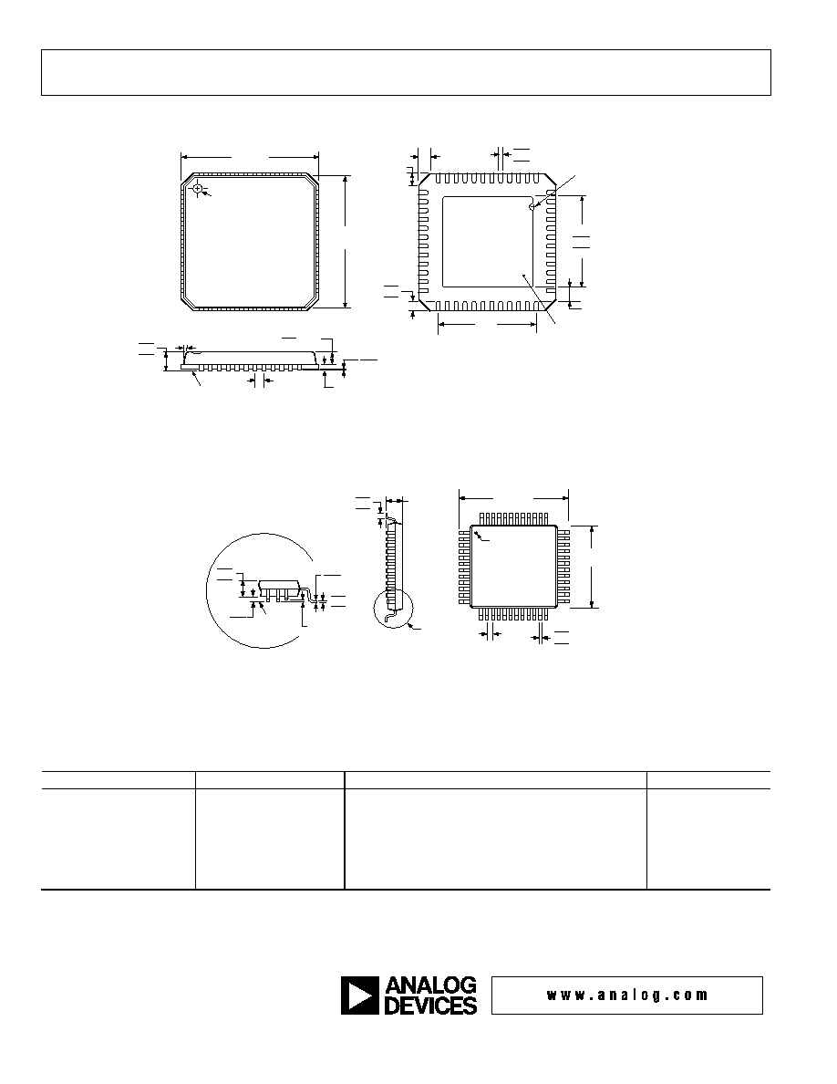
AD7643
Rev. 0 | Page 28 of 28
OUTLINE DIMENSIONS
COMPLIANT TO JEDEC STANDARDS MO-220-VKKD-2
PIN 1
INDICATOR
TOP
VIEW
6.75
BSC SQ
7.00
BSC SQ
1
48
12
13
37
36
24
25
5.25
5.10 SQ
4.95
0.50
0.40
0.30
0.30
0.23
0.18
0.50 BSC
12° MAX
0.20 REF
0.80 MAX
0.65 TYP
1.00
0.85
0.80
5.50
REF
0.05 MAX
0.02 NOM
0.60 MAX
0.60 MAX
PIN 1
INDICATOR
COPLANARITY
0.08
SEATING
PLANE
0.25 MIN
EXPOSED
PAD
(BOTTOM VIEW)
PADDLE CONNECTED TO AGND.
THIS CONNECTION IS NOT
REQUIRED TO MEET THE
ELECTRICAL PERFORMANCES.
Figure 42. 48-Lead Lead Frame Chip Scale Package [LFCSP_VQ]
7 mm × 7 mm Body, Very Thin Quad (CP-48-1)
Dimensions shown in millimeters
COMPLIANT TO JEDEC STANDARDS MS-026-BBC
TOP VIEW
(PINS DOWN)
1
12
13
25
24
36
37
48
0.27
0.22
0.17
0.50
BSC
LEAD PITCH
7.00
BSC SQ
1.60
MAX
0.75
0.60
0.45
VIEW A
9.00
BSC SQ
PIN 1
0.20
0.09
1.45
1.40
1.35
0.08 MAX
COPLANARITY
VIEW A
ROTATED 90° CCW
SEATING
PLANE
7°
3.5°
0°
0.15
0.05
Figure 43. 48-Lead Low Profile Quad Flat Package [LQFP]
(ST-48)
Dimensions shown in millimeters
ORDERING GUIDE
Model
Temperature Range
Package Description
Package Option
AD7643BCPZ
1
-40°C to +85°C
48-Lead Lead Frame Chip Scale Package (LFCSP_VQ)
CP-48-1
AD7643BCPZRL
1
-40°C to +85°C
48-Lead Lead Frame Chip Scale Package (LFCSP_VQ)
CP-48-1
AD7643BSTZ
1
-40°C to +85°C
48-Lead Low Profile Quad Flat Package (LQFP)
ST-48
AD7643BSTZRL
1
-40°C to +85°C
48-Lead Low Profile Quad Flat Package (LQFP)
ST-48
EVAL-AD7643CB
2
Evaluation
Board
EVAL-CONTROL BRD3
3
Controller Board
T
1
Z = Pb-free part.
2
This board can be used as a standalone evaluation board or in conjunction with the EVAL-CONTROL BRD3 for evaluation/demonstration purposes.
3
This board allows a PC to control and communicate with all Analog Devices, Inc. evaluation boards ending in the CB designators.
©2006 Analog Devices, Inc. All rights reserved. Trademarks and
registered trademarks are the property of their respective owners.
D0602404/06(0)
TTT
Document Outline
- þÿ
- þÿ
- þÿ
- FUNCTIONAL BLOCK DIAGRAM
- þÿ
- þÿ
- þÿ
- þÿ
- þÿ
- þÿ
- þÿ
- þÿ
- þÿ
- þÿ
- þÿ
- þÿ
- þÿ
- þÿ
- þÿ
- þÿ
- SLAVE SERIAL INTERFACE
- MICROPROCESSOR INTERFACING
- SPI Interface (ADSP-219x)
- þÿ
- þÿ