 | ÐлекÑÑоннÑй компоненÑ: AD7686 | СкаÑаÑÑ:  PDF PDF  ZIP ZIP |
AD7686 16-Bit, 500 kSPS PulSAR ADC in MSOP/QFN Data Sheet (Rev. 0)
16-Bit, 500 kSPS PulSARTM
ADC in MSOP/QFN
AD7686
Rev. 0
Information furnished by Analog Devices is believed to be accurate and reliable.
However, no responsibility is assumed by Analog Devices for its use, nor for any
infringements of patents or other rights of third parties that may result from its use.
Specifications subject to change without notice. No license is granted by implication
or otherwise under any patent or patent rights of Analog Devices. Trademarks and
registered trademarks are the property of their respective owners.
One Technology Way, P.O. Box 9106, Norwood, MA 02062-9106, U.S.A.
Tel: 781.329.4700
www.analog.com
Fax: 781.461.3113
©2005 Analog Devices, Inc. All rights reserved.
FEATURES
16-bit resolution with no missing codes
Throughput: 500 kSPS
INL: ±0.6 LSB typ, ±2 LSB max (±0.003% of FSR)
S/(N + D): 92.5 dB @ 20 kHz
THD: -110 dB @ 20 kHz
Pseudo-differential analog input range
0 V to V
REF
with V
REF
up to VDD
No pipeline delay
Single-supply 5 V operation with
1.8 V/2.5 V/3 V/5 V logic interface
Serial interface SPI®/QSPITM/MICROWIRETM/DSP-compatible
Daisy-chain multiple ADCs and BUSY indicator
Power dissipation
3.75 mW @ 5 V/100 kSPS
3.75 µW @ 5 V/100 SPS
Standby current: 1 nA
10-lead MSOP (MSOP-8 size) and
3 mm × 3 mm QFN
1
(LFCSP) (SOT-23 size)
Pin-for-pin compatible with AD7685, AD7687, and AD7688
APPLICATIONS
Battery-powered equipment
Data acquisitions
Instrumentation
Medical instruments
Process controls
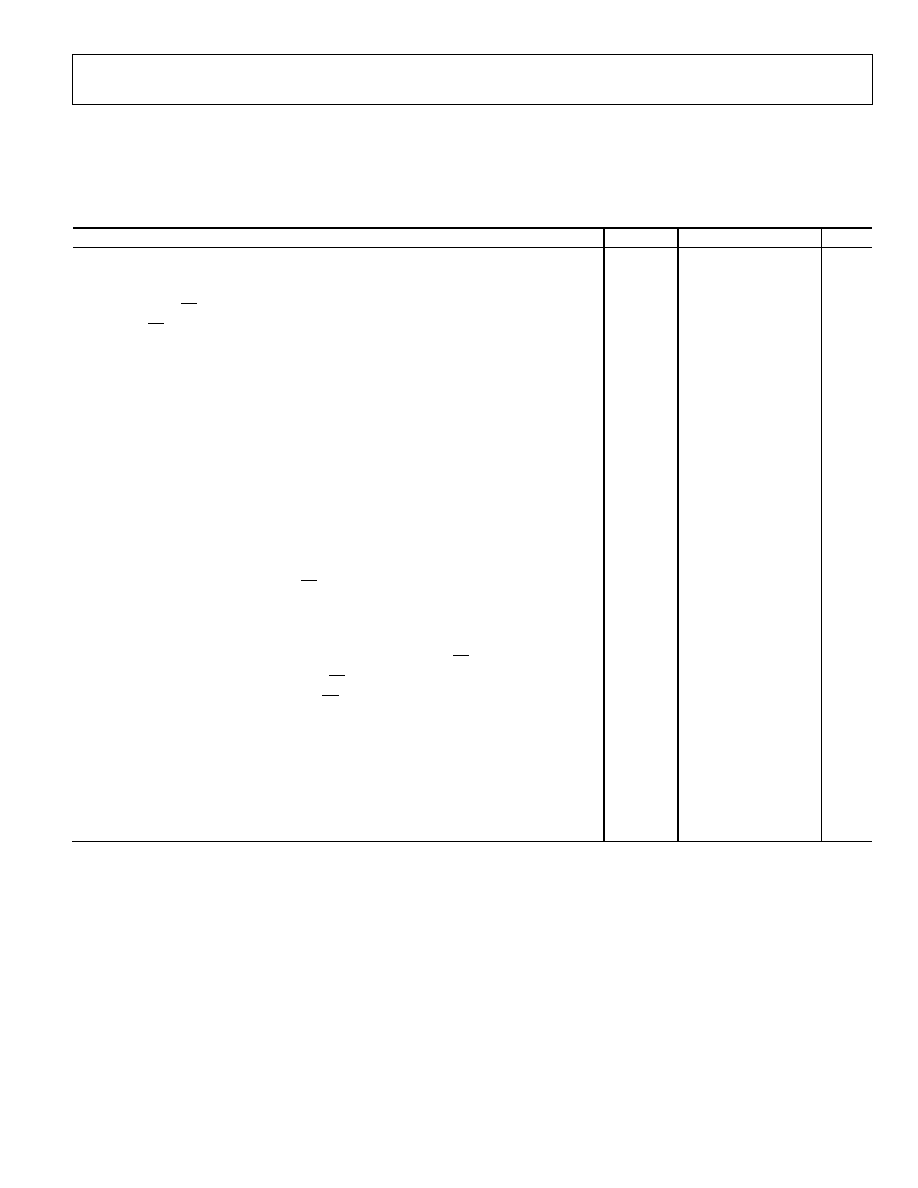
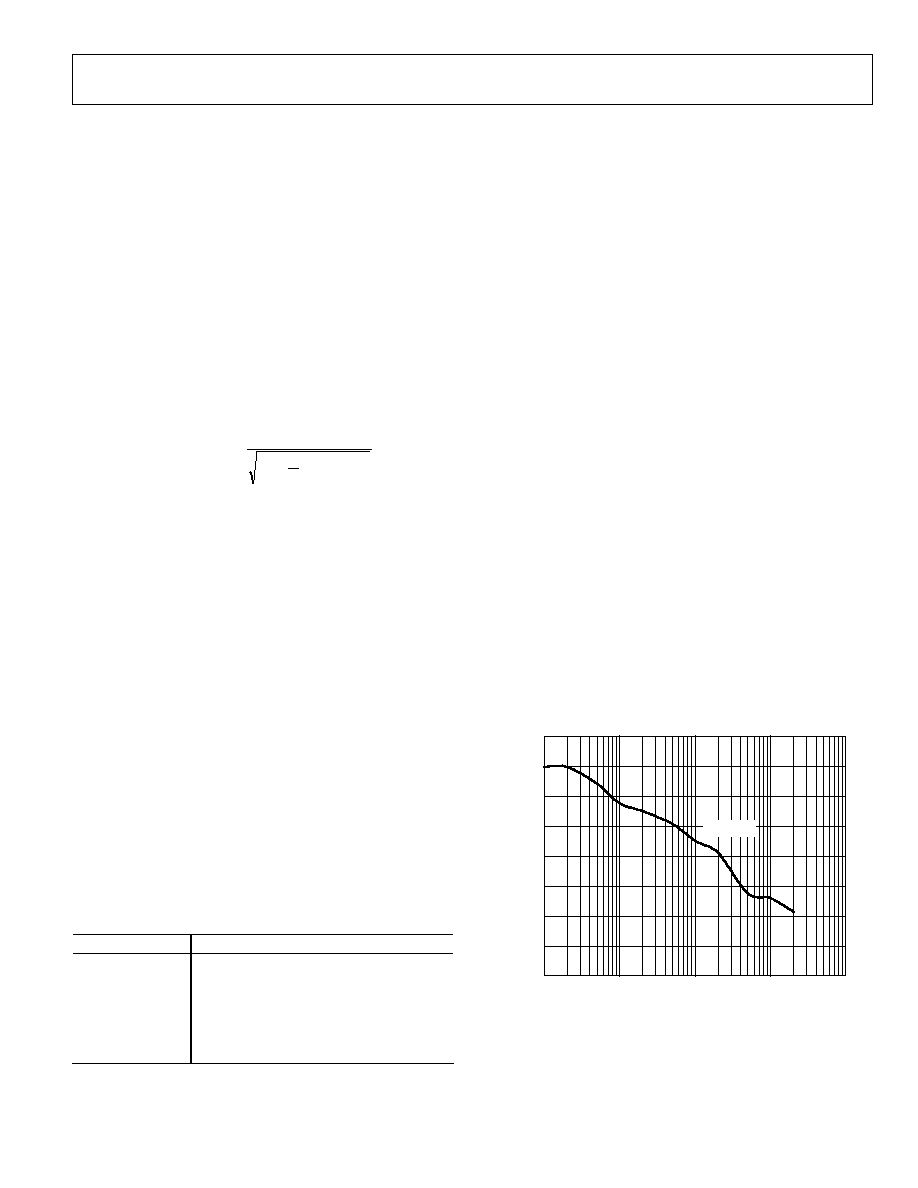
CODE
INL (LSB)
2.0
1.5
1.0
0.5
0
0.5
1.0
1.5
2.0
0
16384
32768
49152
65535
02969-
007
POSITIVE INL = +0.52LSB
NEGATIVE INL = 0.38LSB
Figure 1. Integral Nonlinearity vs. Code
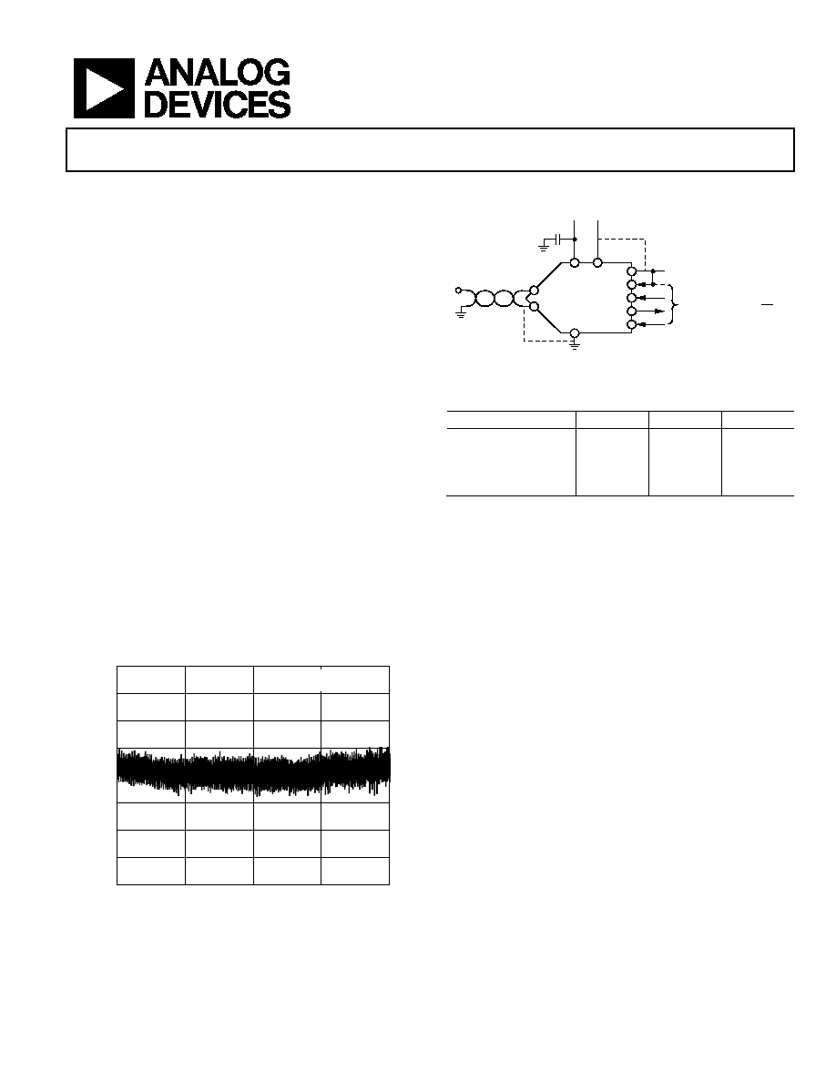
APPLICATION DIAGRAM
AD7686
REF
GND
VDD
IN+
IN
VIO
SDI
SCK
SDO
CNV
1.8V TO VDD
3- OR 4-WIRE INTERFACE
(SPI, DAISY CHAIN, CS)
0.5V TO 5V
5V
0 TO VREF
02969-002
Figure 2.
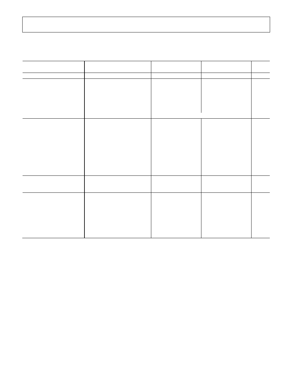
Table 1. MSOP, QFN
1
(LFCSP)/SOT-23 16-Bit PulSAR ADC
Type
100 kSPS
250 kSPS
500 kSPS
True Differential
AD7684
AD7687
AD7688
Pseudo
AD7683
AD7685
AD7686
Differential/Unipolar
AD7694
Unipolar
AD7680
GENERAL DESCRIPTION
The AD7686 is a 16-bit, charge redistribution, successive
approximation, analog-to-digital converter (ADC) that operates
from a single 5 V power supply, VDD. It contains a low power,
high speed, 16-bit sampling ADC with no missing codes, an
internal conversion clock, and a versatile serial interface port.
The part also contains a low noise, wide bandwidth, short
aperture delay track-and-hold circuit. On the CNV rising edge,
it samples an analog input IN+ between 0 V to REF with respect
to a ground sense IN-. The reference voltage, REF, is applied
externally and can be set up to the supply voltage.
Its power scales linearly with throughput.
The SPI-compatible serial interface also features the ability,
using the SDI input, to daisy-chain several ADCs on a single,
3-wire bus or provides an optional BUSY indicator. It is
compatible with 1.8 V, 2.5 V, 3 V, or 5 V logic, using the separate
supply VIO.
The AD7686 is housed in a 10-lead MSOP or a 10-lead QFN
1
(LFCSP) with operation specified from -40°C to +85°C.
1
QFN package in development. Contact sales for samples and availability.

AD7686
Rev 0 | Page 2 of 28
TABLE OF CONTENTS
Specifications..................................................................................... 3
Timing Specifications....................................................................... 5
Absolute Maximum Ratings............................................................ 6
ESD Caution.................................................................................. 6
Pin Configuration and Function Descriptions............................. 7
Terminology ...................................................................................... 8
Typical Performance Characteristics ............................................. 9
Circuit Information.................................................................... 12
Converter Operation.................................................................. 12
Typical Connection Diagram ................................................... 13
Analog Input ............................................................................... 14
Driver Amplifier Choice............................................................ 15
Voltage Reference Input............................................................. 15
Power Supply............................................................................... 15
Supplying the ADC from the Reference.................................. 16
Digital Interface.......................................................................... 16
CS MODE 3-Wire, No BUSY Indicator .................................. 17
CS Mode 3-Wire with BUSY Indicator ................................... 18
CS Mode 4-Wire with BUSY Indicator ................................... 20
Chain Mode, No BUSY Indicator ............................................ 21
Chain Mode with BUSY Indicator ........................................... 22
Application Hints ........................................................................... 23
Layout .......................................................................................... 23
Evaluating the AD7686's Performance.................................... 23
True 16-Bit Isolated Application Example .............................. 24
Outline Dimensions ....................................................................... 25
Ordering Guide .......................................................................... 26
REVISION HISTORY
4/05--Revision 0: Initial Version
AD7686
Rev 0 | Page 3 of 28
SPECIFICATIONS
VDD = 4.5 V to 5.5 V, VIO = 2.3 V to VDD, V
REF
= VDD, T
A
= 40°C to +85°C, unless otherwise noted.
Table 2.
B Grade
C Grade
Parameter
Conditions
Min Typ Max
Min Typ Max
Unit
RESOLUTION
16
16
Bits
ANALOG
INPUT
Voltage Range
IN+ - IN-
0
V
REF
0
V
REF
V
Absolute Input Voltage
IN+
-0.1
VDD + 0.1
-0.1
VDD + 0.1
V
IN-
-0.1
+0.1
-0.1
+0.1
V
Analog Input CMRR
f
IN
= 200 kHz
65
65
dB
Leakage Current at 25°C
Acquisition
phase
1
1
nA
Input Impedance
See the Analog Input section
ACCURACY
No Missing Codes
16
16
Bits
Differential Linearity Error
-1
±0.7
-1
±0.5
+1.5
LSB
1
Integral Linearity Error
-3
±1
+3
-2
±0.6
+2
LSB
Transition Noise
REF = VDD = 5 V
0.5
0.45
LSB
Gain Error
2
, T
MIN
to T
MAX
±2
±8
±2
±6
LSB
Gain Error Temperature Drift
±0.3
±0.3
ppm/°C
Offset Error
2
, T
MIN
to T
MAX
±0.1
±1.6 ±0.1
±1.6 mV
Offset Temperature Drift
±0.3
±0.3
ppm/°C
Power Supply Sensitivity
VDD = 5 V
± 5%
±0.05
±0.05
LSB
THROUGHPUT
Conversion
Rate
0
500
0
500
kSPS
Transient Response
Full-scale step
400
400
ns
AC
ACCURACY
Signal-to-Noise Ratio
f
IN
= 20 kHz, V
REF
= 5 V
89
92
91
92.7
dB
3
f
IN
= 20 kHz, V
REF
= 2.5 V
87.5
88
dB
Spurious-Free Dynamic Range
f
IN
= 20 kHz
-106
-110
dB
Total Harmonic Distortion
f
IN
= 20 kHz
-106
-110
dB
Signal-to-(Noise + Distortion)
f
IN
= 20 kHz, V
REF
= 5 V
89
92
91
92.5
dB
f
IN
= 20 kHz, V
REF
= 5 V, -60 dB Input
32
33.5
dB
Intermodulation Distortion
4
-110
-115
dB
1
LSB means least significant bit. With the 5 V input range, one LSB is 76.3 µV.
2
See the Terminology section. These specifications do include full temperature range variation but do not include the error contribution from the external reference.
3
All specifications in dB are referred to a full-scale input FSR. Tested with an input signal at 0.5 dB below full-scale, unless otherwise specified.
4
f
IN1
= 21.4 kHz, f
IN2
= 18.9 kHz, each tone at -7 dB below full-scale.
AD7686
Rev 0 | Page 4 of 28
VDD = 4.5 V to 5.5 V, VIO = 2.3 V to VDD, V
REF
= VDD, T
A
= 40°C to +85°C, unless otherwise noted.
Table 3.
Parameter Conditions
Min
Typ
Max
Unit
REFERENCE
Voltage Range
0.5
VDD + 0.3
V
Load Current
500 kSPS, REF = 5 V
100
µA
SAMPLING DYNAMICS
-3 dB Input Bandwidth
9
MHz
Aperture Delay
VDD = 5 V
2.5
ns
DIGITAL INPUTS
Logic Levels
V
IL
0.3
+0.3 × VIO
V
V
IH
0.7 × VIO
VIO + 0.3
V
I
IL
-1
+1
µA
I
IH
-1
+1
µA
DIGITAL OUTPUTS
Data Format
Serial 16 bits straight binary
Pipeline Delay
Conversion results available immediately
after completed conversion
V
OL
I
SINK
= +500 µA
0.4
V
V
OH
I
SOURCE
= -500 µA
VIO - 0.3
V
POWER SUPPLIES
VDD Specified
performance
4.5
5.5
V
VIO
Specified performance
2.3
VDD + 0.3
V
VIO Range
1.8
VDD + 0.3
V
Standby Current
1, 2
VDD and VIO = 5 V, 25°C
1
50
nA
Power Dissipation
VDD = 5 V, 100 SPS throughput
3.75
µW
VDD = 5 V, 100 kSPS throughput
3.75
4.3
mW
VDD = 5 V, 500 kSPS throughput
21.5
mW
TEMPERATURE RANGE
3
Specified Performance
T
MIN
to T
MAX
-40
+85 °C
1
With all digital inputs forced to VIO or GND as required.
2
During acquisition phase.
3
Contact sales for extended temperature range.
AD7686
Rev 0 | Page 5 of 28
TIMING SPECIFICATIONS
-40°C to +85°C, VDD = 4.5 V to 5.5 V, VIO = 2.3 V to 5.5 V or VDD + 0.3 V, whichever is the lowest, unless otherwise stated.
See Figure 3 and Figure 4 for load conditions.
Table 4.
Parameter
Symbol Min Typ Max Unit
Conversion Time: CNV Rising Edge to Data Available
t
CONV
0.5
1.6 µs
Acquisition Time
t
ACQ
400
ns
Time Between Conversions
t
CYC
2 µs
CNV Pulse Width (CS Mode )
t
CNVH
10
ns
SCK Period (CS Mode )
t
SCK
15
ns
SCK Period (Chain Mode )
t
SCK
VIO Above 4.5 V
17
ns
VIO Above 3 V
18
ns
VIO Above 2.7 V
19
ns
VIO Above 2.3 V
20
ns
SCK Low Time
t
SCKL
7 ns
SCK High Time
t
SCKH
7 ns
SCK Falling Edge to Data Remains Valid
t
HSDO
5 ns
SCK Falling Edge to Data Valid Delay
t
DSDO
VIO Above 4.5 V
14
ns
VIO Above 3 V
15
ns
VIO Above 2.7 V
16
ns
VIO Above 2.3 V
17
ns
CNV or SDI Low to SDO D15 MSB Valid (CS Mode)
t
EN
VIO Above 4.5 V
15
ns
VIO Above 2.7 V
18
ns
VIO Above 2.3 V
22
ns
CNV or SDI High or Last SCK Falling Edge to SDO High Impedance (CS Mode)
t
DIS
25
ns
SDI Valid Setup Time from CNV Rising Edge (CS Mode)
t
SSDICNV
15
ns
SDI Valid Hold Time from CNV Rising Edge (CS Mode)
t
HSDICNV
0 ns
SCK Valid Setup Time from CNV Rising Edge (Chain Mode)
t
SSCKCNV
5 ns
SCK Valid Hold Time from CNV Rising Edge (Chain Mode)
t
HSCKCNV
5 ns
SDI Valid Setup Time from SCK Falling Edge (Chain Mode)
t
SSDISCK
3 ns
SDI Valid Hold Time from SCK Falling Edge (Chain Mode)
t
HSDISCK
4 ns
SDI High to SDO High (Chain Mode with BUSY indicator)
t
DSDOSDI
VIO Above 4.5 V
15
ns
VIO Above 2.3 V
26
ns
AD7686
Rev 0 | Page 6 of 28
ABSOLUTE MAXIMUM RATINGS
Table 5.
Parameter Rating
Analog Inputs
IN+
1
, IN-
1
GND - 0.3 V to VDD + 0.3 V
or ±130 mA
REF
GND - 0.3 V to VDD + 0.3 V
Supply Voltages
VDD, VIO to GND
-0.3 V to +7 V
VDD to VIO
±7 V
Digital Inputs to GND
-0.3 V to VIO + 0.3 V
Digital Outputs to GND
-0.3 V to VIO + 0.3 V
Storage Temperature Range
-65°C to +150°C
Junction Temperature
150°C
JA
Thermal Impedance
200°C/W (MSOP-10)
JC
Thermal Impedance
44°C/W (MSOP-10)
Lead Temperature Range
JEDEC J-STD-20
1
See the
section.
Analog Input
Stresses above those listed under Absolute Maximum Ratings
may cause permanent damage to the device. This is a stress
rating only; functional operation of the device at these or any
other conditions above those indicated in the operational
section of this specification is not implied. Exposure to absolute
maximum rating conditions for extended periods may affect
device reliability.
ESD CAUTION
ESD (electrostatic discharge) sensitive device. Electrostatic charges as high as 4000 V readily accumulate on
the human body and test equipment and can discharge without detection. Although this product features
proprietary ESD protection circuitry, permanent damage may occur on devices subjected to high energy
electrostatic discharges. Therefore, proper ESD precautions are recommended to avoid performance
degradation or loss of functionality.
500
µ
A
I
OL
500
µ
A
I
OH
1.4V
TO SDO
C
L
50pF
02969-
003
Figure 3. Load Circuit for Digital Interface Timing
30% VIO
70% VIO
2V OR VIO 0.5V
1
0.8V OR 0.5V
2
0.8V OR 0.5V
2
2V OR VIO 0.5V
1
t
DELAY
t
DELAY
02969-
004
1
2V IF VIO ABOVE 2.5V, VIO 0.5V IF VIO BELOW 2.5V.
2
0.8V IF VIO ABOVE 2.5V, 0.5V IF VIO BELOW 2.5V.
Figure 4. Voltage Levels for Timing
AD7686
Rev 0 | Page 7 of 28
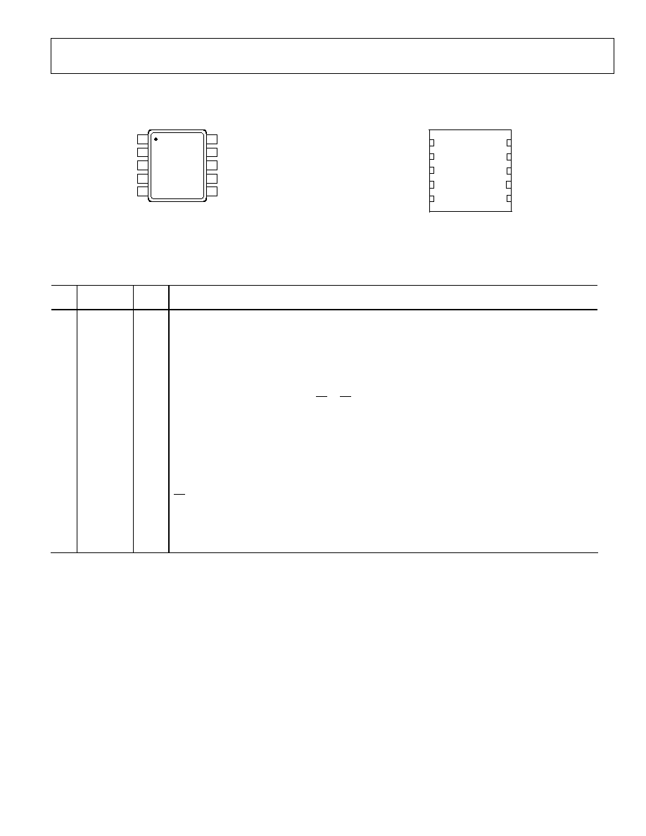
PIN CONFIGURATIONS AND FUNCTION DESCRIPTIONS
02969-
005
REF
1
VDD
2
IN+
3
IN
4
GND
5
VIO
10
SDI
9
SCK
8
SDO
7
CNV
6
AD7686
TOP VIEW
(Not to Scale)
Figure 5. 10-Lead MSOP Pin Configuration
02969-
006
1
REF
2
VDD
3
IN+
4
IN
5
GND
10 VIO
9 SDI
8 SCK
7 SDO
6 CNV
TOP VIEW
(Not to Scale)
AD7686
Figure 6. 10-Lead QFN
1
(LFCSP) Pin Configuration
1
QFN package in development. Contact sales for samples and availability.
Table 6. Pin Function Descriptions
Pin
No. Mnemonic Type
1
Function
1 REF
AI Reference Input Voltage. The REF range is from 0.5 V to VDD. It is referred to the GND pin. This pin should
be decoupled closely to the pin with a 10 µF capacitor.
2 VDD
P
Power
Supply.
3
IN+
AI
Analog Input. It is referred to IN-. The voltage range, that is., the difference between IN+ and IN-, is 0 V to V
REF
.
4
IN-
AI
Analog Input Ground Sense. To be connected to the analog ground plane or to a remote sense ground.
5
GND
P
Power Supply Ground.
6 CNV
DI Convert Input. This input has multiple functions. On its leading edge, it initiates the conversions and
selects the interface mode, chain or CS. In CS mode, it enables the SDO pin when low. In chain mode,
the data should be read when CNV is high.
7
SDO
DO
Serial Data Output. The conversion result is output on this pin. It is synchronized to SCK.
8
SCK
DI
Serial Data Clock Input. When the part is selected, the conversion result is shifted out by this clock.
9
SDI
DI
Serial Data Input. This input provides multiple features. It selects the interface mode of the ADC as follows:
Chain mode is selected if SDI is low during the CNV rising edge. In this mode, SDI is used as a data input
to daisy-chain the conversion results of two or more ADCs onto a single SDO line. The digital data level
on SDI is output on SDO with a delay of 16 SCK cycles.
CS mode is selected if SDI is high during the CNV rising edge. In this mode, either SDI or CNV can enable
the serial output signals when low, and if SDI or CNV is low when the conversion is complete, the BUSY
indicator feature is enabled.
10 VIO
P
Input/Output Interface Digital Power. Nominally at the same supply as the host interface (1.8 V, 2.5 V,
3 V, or 5 V).
1
AI = Analog Input, DI = Digital Input, DO = Digital Output, and P = Power.

AD7686
Rev 0 | Page 8 of 28
TERMINOLOGY
Integral Nonlinearity Error (INL)
It refers to the deviation of each individual code from a line
drawn from negative full scale through positive full scale. The
point used as negative full scale occurs ½ LSB before the first
code transition. Positive full scale is defined as a level 1½ LSB
beyond the last code transition. The deviation is measured from
the middle of each code to the true straight line (Figure 25).
Differential Nonlinearity Error (DNL)
In an ideal ADC, code transitions are 1 LSB apart. DNL is the
maximum deviation from this ideal value. It is often specified in
terms of resolution for which no missing codes are guaranteed.
Offset Error
The first transition should occur at a level ½ LSB above analog
ground (38.1 µV for the 0 V to 5 V range). The offset error is
the deviation of the actual transition from that point.
Gain Error
The last transition (from 111 . . . 10 to 111 . . . 11) should occur
for an analog voltage 1½ LSB below the nominal full scale
(4.999886 V for the 0 V to 5 V range). The gain error is the
deviation of the actual level of the last transition from the ideal
level after the offset has been adjusted out.
Spurious-Free Dynamic Range (SFDR)
SFDR is the difference, in decibels (dB), between the rms
amplitude of the input signal and the peak spurious signal.
Effective Number of Bits (ENOB)
ENOB is a measurement of the resolution with a sine wave
input. It is related to S/(N+D) by the following formula
ENOB = (S/[N + D]
dB
- 1.76)/6.02
and is expressed in bits.
Total Harmonic Distortion (THD)
THD is the ratio of the rms sum of the first five harmonic
components to the rms value of a full-scale input signal and is
expressed in dB.
Signal-to-Noise Ratio (SNR)
SNR is the ratio of the rms value of the actual input signal to the
rms sum of all other spectral components below the Nyquist
frequency, excluding harmonics and dc. The value for SNR is
expressed in dB.
Signal-to-(Noise + Distortion) Ratio (S/[N+D])
S/(N+D) is the ratio of the rms value of the actual input signal
to the rms sum of all other spectral components below the
Nyquist frequency, including harmonics but excluding dc. The
value for S/(N+D) is expressed in dB.
Aperture Delay
It is the measure of the acquisition performance and is the time
between the rising edge of the CNV input and when the input
signal is held for a conversion.
Transient Response
It is the time required for the ADC to accurately acquire its
input after a full-scale step function was applied.
AD7686
Rev 0 | Page 9 of 28
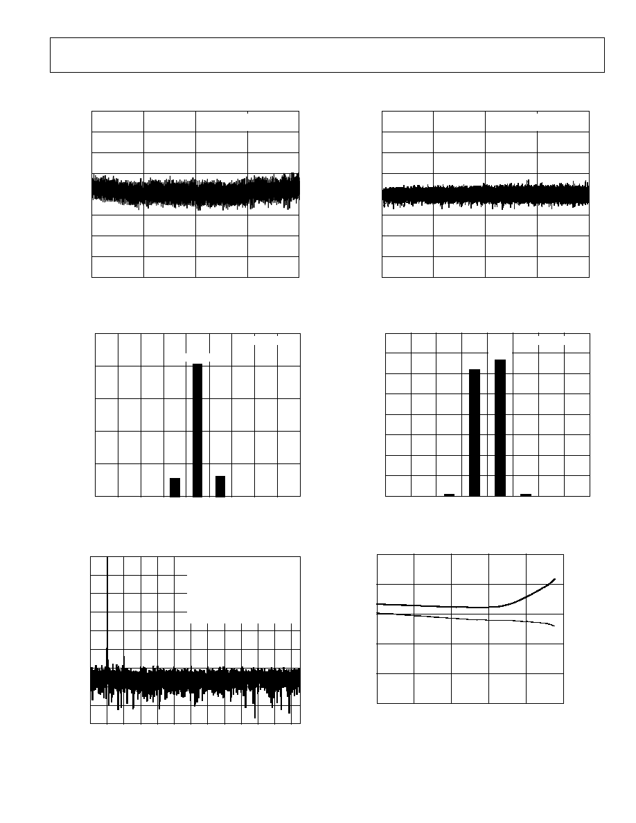
TYPICAL PERFORMANCE CHARACTERISTICS
CODE
INL (LSB)
2.0
1.5
1.0
0.5
0
0.5
1.0
1.5
2.0
0
16384
32768
49152
65535
02969-
007
POSITIVE INL = +0.52LSB
NEGATIVE INL = 0.38LSB
Figure 7. Integral Nonlinearity vs. Code
02969-
008
COUNTS
250000
200000
150000
100000
50000
0
CODE IN HEX
802B 802C 802D 802E
8026 8027 8028 8029 802A
0
0
26
0
0
202719
30770
27583
22
VDD = REF = 5V
Figure 8. Histogram of a DC Input at the Code Center
02969-009
FREQUENCY (kHz)
120
0
20
40
60
80 100
200 220 240
140 160 180
AMPLITUDE (dB OF FULL SCALE)
0
20
40
60
80
100
120
160
140
180
8192 POINT FFT
VDD = REF = 5V
f
S
= 500kSPS
f
IN
= 19.99kHz
SNR = 92.8dB
THD = 108.7dB
SECOND HARMONIC = 110.1dB
THIRD HARMONIC = 119.2dB
Figure 9. FFT Plot
CODE
DNL (LSB)
2.0
1.5
1.0
0.5
0
0.5
1.0
1.5
2.0
0
16384
32768
49152
65535
02969-
010
POSITIVE DNL = +0.35LSB
NEGATIVE DNL = 0.36LSB
Figure 10. Differential Nonlinearity vs. Code
02969-
011
COUNTS
160000
140000
120000
100000
60000
80000
20000
40000
0
CODE IN HEX
802B
8024
8026
8025
8027
8028
8029
802A
0
0
1703
0
0
124164
133575
1678
VDD = REF = 5V
Figure 11. Histogram of a DC Input at the Code Transition
02969-012
INPUT LEVEL (dB)
0
10
8
6
4
2
THD (dB)
120
105
108
111
114
117
S
NR (dB)
95
94
93
92
91
90
SNR
THD
Figure 12. SNR and THD vs. Input Level
AD7686
Rev 0 | Page 10 of 28
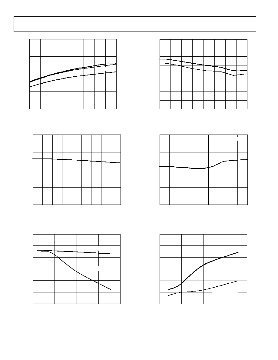
02969-
013
REFERENCE VOLTAGE (V)
5.5
2.3
2.7
3.5
4.3
5.1
3.1
3.9
4.7
SNR, S/(
N
+ D)
(
d
B)
100
95
85
90
70
SNR
ENOB
ENOB (
B
it
s
)
17.0
15.0
16.0
14.0
13.0
S/[N + D]
Figure 13. SNR, S/(N + D), and ENOB vs. Reference Voltage
02969-014
TEMPERATURE (
°
C)
125
55
35
15
5
25
45
65
85
105
S
NR (
d
B)
100
95
90
85
80
VREF = 5V
Figure 14. SNR vs. Temperature
02969-015
FREQUENCY (kHz)
200
0
50
100
150
S
/
(N +
D) (d
B)
100
95
85
90
80
75
70
VREF = 5V, 10dB
VREF = 5V, 1dB
Figure 15. S/(N + D) vs. Frequency
02969-016
REFERENCE VOLTAGE (V)
5.5
2.3
2.7
3.5
4.3
5.1
3.1
3.9
4.7
THD, SFDR (dB)
90
95
100
105
110
115
120
125
130
THD
SFDR
Figure 16. THD, SFDR vs. Reference Voltage
02969-017
TEMPERATURE (
°
C)
125
55
35
15
5
25
45
65
85
105
T
HD (
d
B)
90
100
110
120
130
VREF = 5V
Figure 17. THD vs. Temperature
02969-018
FREQUENCY (kHz)
200
0
50
100
150
THD (
d
B)
60
70
90
80
100
110
120
VREF = 5V, 10dB
VREF = 5V, 1dB
Figure 18. THD vs. Frequency
AD7686
Rev 0 | Page 11 of 28
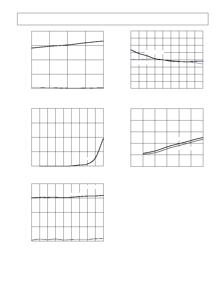
SUPPLY (V)
O
PERATING
CURRENT (
µ
A)
1000
750
500
250
0
4.50
4.75
5.00
5.25
5.50
02969-
019
VIO
VDD
f
S
= 100kSPS
Figure 19. Operating Currents vs. Supply
TEMPERATURE (
°
C)
PO
WER-DO
WN CURRENT (nA)
1000
750
500
250
0
55
35
15
5
25
45
65
85
105
125
02969-
020
VDD + VIO
Figure 20. Power-Down Currents vs. Temperature
TEMPERATURE (
°
C)
O
PERATING
CURRENT (
µ
A)
1000
750
500
250
0
55
35
15
5
25
45
65
85
105
125
02969-
021
VIO
VDD = 5V
f
S
= 100kSPS
Figure 21. Operating Currents vs. Temperature
02969-
022
TEMPERATURE (
°
C)
125
55
35
5
45
105
85
15
25
65
OF
F
SET
, GAIN ERROR (
L
SB)
4
3
2
1
0
1
2
3
4
OFFSET ERROR
GAIN ERROR
Figure 22. Offset and Gain Error vs. Temperature
02969-
023
SDO CAPACITIVE LOAD (pF)
120
0
20
40
60
80
100
T
DSDO
DELAY (ns)
25
20
15
10
5
0
VDD = 5V, 85°C
VDD = 5V, 25°C
Figure 23. t
DSDO
Delay vs. Capacitance Load and Supply
AD7686
Rev 0 | Page 12 of 28
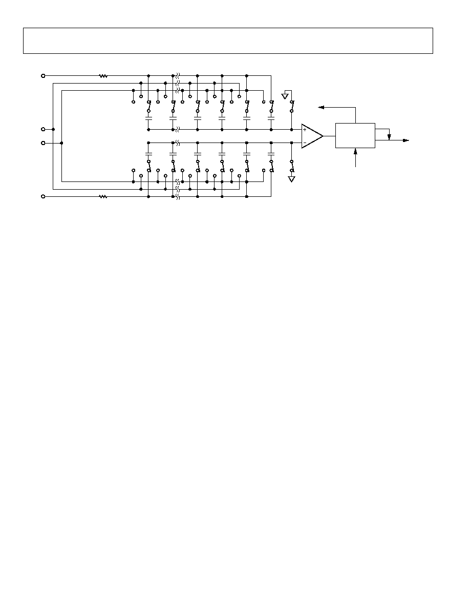
SW+
MSB
16,384C
IN+
LSB
COMP
CONTROL
LOGIC
SWITCHES CONTROL
BUSY
OUTPUT CODE
CNV
REF
GND
IN
4C
2C
C
C
32,768C
SW
MSB
16,384C
LSB
4C
2C
C
C
32,768C
02969-
024
Figure 24. ADC Simplified Schematic
CIRCUIT INFORMATION
The AD7686 is a fast, low power, single-supply, precise 16-bit
ADC using a successive approximation architecture.
The AD7686 is capable of converting 500,000 samples per
second (500 kSPS) and powers down between conversions.
When operating at 100 SPS, for example, it consumes 3.75 µW
typically, ideal for battery-powered applications.
The AD7686 provides the user with an on-chip track-and-hold
and does not exhibit any pipeline delay or latency, making it
ideal for multiple multiplexed channel applications.
The AD7686 is specified from 4.5 V to 5.5 V and can be
interfaced to any of the 1.8 V to 5 V digital logic family. It is
housed in a 10-lead MSOP or a tiny 10-lead QFN
1
(LFCSP) that
combines space savings and allows flexible configurations.
It is pin-for-pin-compatible with the
AD7685
,
AD7687
, and
AD7688
.
1.
QFN package in development. Contact sales for samples and availability.
CONVERTER OPERATION
The AD7686 is a successive approximation ADC based on a
charge redistribution DAC. Figure 24 shows the simplified
schematic of the ADC. The capacitive DAC consists of two
identical arrays of 16 binary weighted capacitors, which are
connected to the two comparator inputs.
During the acquisition phase, terminals of the array tied to the
comparator's input are connected to GND via SW+ and SW-.
All independent switches are connected to the analog inputs.
Thus, the capacitor arrays are used as sampling capacitors and
acquire the analog signal on the IN+ and IN- inputs. When the
acquisition phase is complete and the CNV input goes high, a
conversion phase is initiated. When the conversion phase
begins, SW+ and SW- are opened first. The two capacitor
arrays are then disconnected from the inputs and connected to
the GND input. Therefore, the differential voltage between the
inputs IN+ and IN- captured at the end of the acquisition phase
is applied to the comparator inputs, causing the comparator to
become unbalanced. By switching each element of the capacitor
array between GND and REF, the comparator input varies by
binary weighted voltage steps (V
REF
/2, V
REF
/4 . . . V
REF
/65536).
The control logic toggles these switches, starting with the MSB,
in order to bring the comparator back into a balanced
condition. After the completion of this process, the part returns
to the acquisition phase and the control logic generates the
ADC output code and a BUSY signal indicator.
Because the AD7686 has an on-board conversion clock, the
serial clock, SCK, is not required for the conversion process.
AD7686
Rev 0 | Page 13 of 28
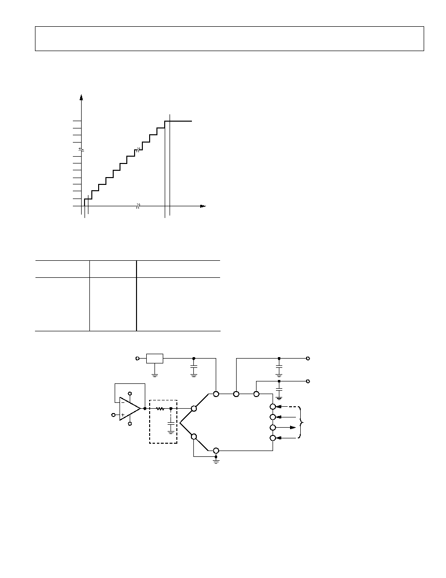
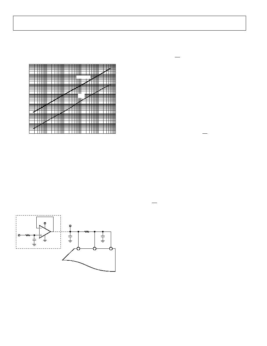
Transfer Functions
The ideal transfer characteristic for the AD7686 is shown in
Figure 25 and Table 7.
000...000
000...001
000...010
111...101
111...110
111...111
ADC CO
DE (STRAIG
H
T BINARY)
ANALOG INPUT
+FSR 1.5 LSB
+FSR 1 LSB
FSR + 1 LSB
FSR
FSR + 0.5 LSB
02969-
025
Figure 25. ADC Ideal Transfer Function
Table 7. Output Codes and Ideal Input Voltages
Description
Analog Input
V
REF
= 5 V
Digital Output Code Hexa
FSR 1 LSB
4.999924 V
FFFF
1
Midscale + 1 LSB 2.500076 V
8001
Midscale
2.5 V
8000
Midscale 1 LSB
2.499924 V
7FFF
FSR + 1 LSB
76.3 µV
0001
FSR
0 V
0000
2
TYPICAL CONNECTION DIAGRAM
Figure 26 shows an example of the recommended connection
diagram for the AD7686 when multiple supplies are available.
1.
This is also the code for an overranged analog input (V
IN+
- V
IN-
above V
REF
-
V
GND
).
2.
This is also the code for an underranged analog input (V
IN+
- V
IN-
below V
GND
).
AD7686
REF
GND
VDD
IN
IN+
VIO
SDI
SCK
SDO
CNV
3- OR 4-WIRE INTERFACE
5
100nF
100nF
5V
10
µ
F
2
7V
7V
2V
1.8V TO VDD
REF
1
0 TO VREF
33
2.7nF
3
4
02969-
026
1
SEE REFERENCE SECTION FOR REFERENCE SELECTION.
2
C
REF
IS USUALLY A 10
µ
F CERAMIC CAPACITOR (X5R).
3
SEE DRIVER AMPLIFIER CHOICE SECTION.
4
OPTIONAL FILTER. SEE ANALOG INPUT SECTION.
5
SEE DIGITAL INTERFACE FOR MOST CONVENIENT INTERFACE MODE.
Figure 26. Typical Application Diagram with Multiple Supplies
AD7686
Rev 0 | Page 14 of 28
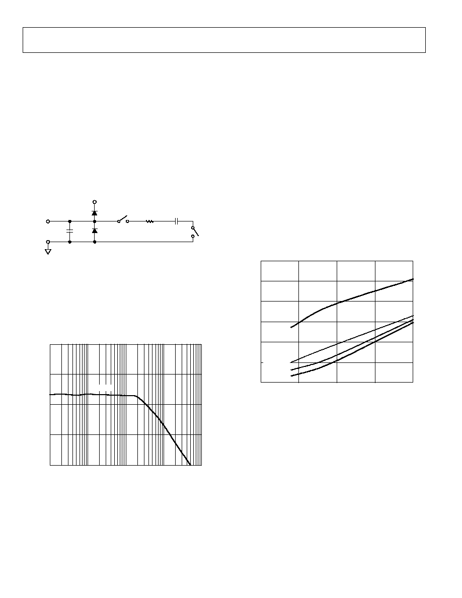
ANALOG INPUT
Figure 27 shows an equivalent circuit of the input structure of
the AD7686.
The two diodes, D1 and D2, provide ESD protection for the
analog inputs IN+ and IN-. Care must be taken to ensure that
the analog input signal never exceeds the supply rails by more
than 0.3 V because this causes these diodes to begin to forward-
bias and start conducting current. These diodes can handle a
forward-biased current of 130 mA maximum. For instance,
these conditions could eventually occur when the input buffer's
(U1) supplies are different from VDD. In such a case, an input
buffer with a short-circuit current limitation can be used to
protect the part.
C
IN
R
IN
D1
D2
C
PIN
IN+
OR IN
GND
VDD
02969-027
Figure 27. Equivalent Analog Input Circuit
The analog input structure allows the sampling of the
differential signal between IN+ and IN-. By using this
differential input, small signals common to both inputs are
rejected, as shown in Figure 28, which represents the typical
CMRR over frequency. For instance, by using IN- to sense a
remote signal ground, ground potential differences between the
sensor and the local ADC ground are eliminated.
02969-
028
FREQUENCY (kHz)
10000
1
10
100
1000
CMRR (
d
B)
80
70
60
50
40
VDD = 5V
Figure 28. Analog Input CMRR vs. Frequency
During the acquisition phase, the impedance of the analog
inputs (IN+ or IN-) can be modeled as a parallel combination
of capacitor, C
PIN
, and the network formed by the series
connection of R
IN
and C
IN
. C
PIN
is primarily the pin capacitance.
R
IN
is typically 600 and is a lumped component made up of
some serial resistors and the on resistance of the switches. C
IN
is
typically 30 pF and is mainly the ADC sampling capacitor.
During the conversion phase, where the switches are opened,
the input impedance is limited to C
PIN
. R
IN
and C
IN
make a
1-pole, low-pass filter that reduces undesirable aliasing effects
and limits the noise.
When the source impedance of the driving circuit is low, the
AD7686 can be driven directly. Large source impedances
significantly affect the ac performance, especially total
harmonic distortion (THD). The dc performances are less
sensitive to the input impedance. The maximum source
impedance depends on the amount of THD that can be
tolerated. The THD degrades as a function of the source
impedance and the maximum input frequency, as shown in
Figure 29.
02969-
030
FREQUENCY (kHz)
100
0
25
50
75
THD (dB)
80
85
90
95
100
105
110
R
S
= 33
R
S
= 50
R
S
= 100
R
S
= 250
Figure 29. THD vs. Analog Input Frequency and Source Resistance
AD7686
Rev 0 | Page 15 of 28
DRIVER AMPLIFIER CHOICE
Although the AD7686 is easy to drive, the driver amplifier
needs to meet the following requirements:
·
The noise generated by the driver amplifier needs to be
kept as low as possible in order to preserve the SNR and
transition noise performance of the AD7686. Note that
the AD7686 has a noise much lower than most of the other
16-bit ADCs and, therefore, can be driven by a noisier
amplifier in order to meet a given system noise
specification. The noise coming from the amplifier is
filtered by the AD7686 analog input circuit 1-pole, low-
pass filter made by R
IN
and C
IN
or by the external filter, if
one is used. Because the typical noise of the AD7686 is
37 µV rms, the SNR degradation due to the amplifier is
+
=
-
2
2
)
(
2
37
37
20log
N
3dB
LOSS
Ne
f
SNR
where:
f
3dB
is the input bandwidth in MHz of the AD7686
(9 MHz) or the cutoff frequency of the input filter, if
one is used.
N is the noise gain of the amplifier (for example, +1 in
buffer configuration).
e
N
is the equivalent input noise voltage of the op amp, in
nV/Hz.
·
For ac applications, the driver should have a THD
performance commensurate with the AD7686. Figure 18
shows the THD vs. frequency that the driver should
exceed.
·
For multichannel multiplexed applications, the driver
amplifier and the AD7686 analog input circuit must settle a
full-scale step onto the capacitor array at a 16-bit level
(0.0015%). In the amplifier's data sheet, settling at 0.1% to
0.01% is more commonly specified. This could differ
significantly from the settling time at a 16-bit level and
should be verified prior to driver selection.
Table 8. Recommended Driver Amplifiers.
Amplifier
Typical Application
AD8021
Very low noise and high frequency
AD8022
Low noise and high frequency
OP184
Low power, low noise, and low frequency
AD8605
,
AD8615
5 V single-supply, low power
AD8519
Small, low power and low frequency
AD8031
High frequency and low power
VOLTAGE REFERENCE INPUT
The AD7686 voltage reference input, REF, has a dynamic input
impedance and should therefore be driven by a low impedance
source with efficient decoupling between the REF and GND
pins, as explained in the Layout section.
When REF is driven by a very low impedance source, for
example, a reference buffer using the AD8031 or the AD8605, a
10 µF (X5R, 0805 size) ceramic chip capacitor is appropriate for
optimum performance.
If an unbuffered reference voltage is used, the decoupling value
depends on the reference used. For instance, a 22 µF (X5R,
1206 size) ceramic chip capacitor is appropriate for optimum
performance using a low temperature drift ADR43x reference.
If desired, smaller reference decoupling capacitor values down
to 2.2 µF can be used with a minimal impact on performance,
especially DNL.
Regardless, there is no need for an additional lower value
ceramic decoupling capacitor (for example, 100 nF) between the
REF and GND pins.
POWER SUPPLY
The AD7686 is specified at 4.5 V to 5.5 V. It uses two power
supply pins: a core supply VDD and a digital input/output
interface supply VIO. VIO allows direct interface with any
logic between 1.8 V and VDD. To reduce the supplies needed,
the VIO and VDD can be tied together. The AD7686 is
independent of power supply sequencing between VIO and
VDD. Additionally, it is very insensitive to power supply
variations over a wide frequency range, as shown in Figure 30,
which represents PSRR over frequency.
02969-
031
FREQUENCY (kHz)
10000
1
1000
10
100
P
S
RR (
d
B)
110
100
90
80
70
60
50
40
30
VDD =5V
Figure 30. PSRR vs. Frequency
AD7686
Rev 0 | Page 16 of 28
The AD7686 powers down automatically at the end of each
conversion phase and, therefore, the power scales linearly with
the sampling rate, as shown in Figure 31. This makes the part
ideal for low sampling rate (even a few Hz) and low battery-
powered applications.
SAMPLING RATE (SPS)
OPERATI
N
G CURRENT (
µ
A)
1000
10
0.1
0.001
10
100
1000
10000
100000
1000000
02969-
032
VIO
VDD = 5V
Figure 31. Operating Currents vs. Sampling Rate
SUPPLYING THE ADC FROM THE REFERENCE
For simplified applications, the AD7686, with its low operating
current, can be supplied directly using the reference circuit
shown in Figure 32. The reference line can be driven by either:
·
The system power supply directly.
·
A reference voltage with enough current output capability,
such as the ADR43x.
·
A reference buffer, such as the AD8031, which can also
filter the system power supply, as shown in Figure 32.
AD8031
AD7686
VIO
REF
VDD
10
µ
F
1
µ
F
10
10k
5V
5V
5V
1
µ
F
1
02969-
033
1
OPTIONAL REFERENCE BUFFER AND FILTER.
Figure 32. Example of Application Circuit
DIGITAL INTERFACE
Though the AD7686 has a reduced number of pins, it offers
flexibility in its serial interface modes.
The AD7686, when in CS mode, is compatible with SPI, QSPI,
digital hosts, and DSPs, for example, Blackfin® ADSP-BF53x or
ADSP-219x. This interface can use either 3-wire or 4-wire. A 3-
wire interface using the CNV, SCK, and SDO signals minimizes
wiring connections useful, for instance, in isolated applications.
A 4-wire interface using the SDI, CNV, SCK, and SDO signals
allows CNV, which initiates the conversions, to be independent
of the readback timing (SDI). This is useful in low jitter
sampling or simultaneous sampling applications.
The AD7686, when in chain mode, provides a daisy chain
feature using the SDI input for cascading multiple ADCs on a
single data line similar to a shift register.
The mode in which the part operates depends on the SDI level
when the CNV rising edge occurs. The CS mode is selected if
SDI is high and the chain mode is selected if SDI is low. The
SDI hold time is such that when SDI and CNV are connected
together, the chain mode is always selected.
In either mode, the AD7686 offers the flexibility to optionally
force a start bit in front of the data bits. This start bit can be
used as a BUSY signal indicator to interrupt the digital host and
trigger the data reading. Otherwise, without a BUSY indicator,
the user must time out the maximum conversion time prior to
readback.
The BUSY indicator feature is enabled as:
·
In the CS mode, if CNV or SDI is low when the ADC
conversion ends (Figure 36 and Figure 40).
·
In the chain mode, if SCK is high during the CNV rising edge
(Figure 44).
AD7686
Rev 0 | Page 17 of 28
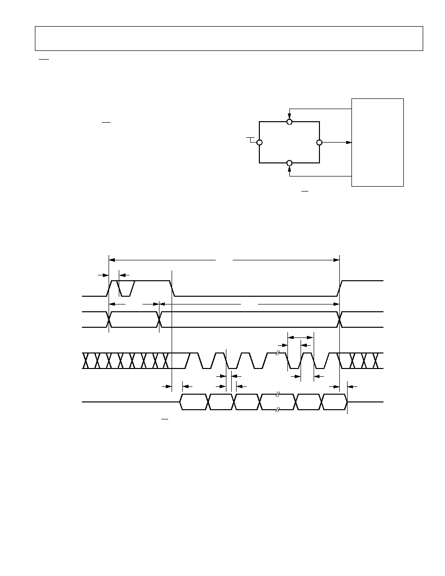
CS MODE 3-WIRE, NO BUSY INDICATOR
This mode is usually used when a single AD7686 is connected
to an SPI-compatible digital host. The connection diagram is
shown in Figure 33 and the corresponding timing is given in
Figure 34.
With SDI tied to VIO, a rising edge on CNV initiates a
conversion, selects the CS mode, and forces SDO to high
impedance. Once a conversion is initiated, it continues to
completion irrespective of the state of CNV. For instance, it
could be useful to bring CNV low to select other SPI devices,
such as analog multiplexers, but CNV must be returned high
before the minimum conversion time and held high until the
maximum conversion time to avoid the generation of the BUSY
signal indicator. When the conversion is complete, the AD7686
enters the acquisition phase and powers down. When CNV
goes low, the MSB is output onto SDO. The remaining data bits
are then clocked by subsequent SCK falling edges. The data is
valid on both SCK edges. Although the rising edge can be used
to capture the data, a digital host using the SCK falling edge
allows a faster reading rate provided it has an acceptable hold
time. After the 16th SCK falling edge or when CNV goes high,
whichever is earlier, SDO returns to high impedance.
CNV
SCK
SDO
SDI
DATA IN
CLK
CONVERT
VIO
DIGITAL HOST
AD7686
02969-034
Figure 33. CS Mode 3-Wire, No BUSY Indicator
Connection Diagram (SDI High)
SDO
D15
D14
D13
D1
D0
t
DIS
SCK
1
2
3
14
15
16
t
SCK
t
SCKL
t
SCKH
t
HSDO
t
DSDO
CNV
CONVERSION
ACQUISITION
t
CONV
t
CYC
ACQUISITION
SDI = 1
t
CNVH
t
ACQ
t
EN
02969-
035
Figure 34. CS Mode 3-Wire, No BUSY Indicator Serial Interface Timing (SDI High)
AD7686
Rev 0 | Page 18 of 28
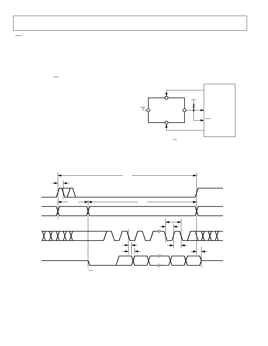
CS MODE 3-WIRE WITH BUSY INDICATOR
This mode is usually used when a single AD7686 is connected
to an SPI-compatible digital host having an interrupt input.
The connection diagram is shown in Figure 35 and the
corresponding timing is given in Figure 36.
With SDI tied to VIO, a rising edge on CNV initiates a
conversion, selects the CS mode, and forces SDO to high
impedance. SDO is maintained in high impedance until the
completion of the conversion irrespective of the state of CNV.
Prior to the minimum conversion time, CNV could be used to
select other SPI devices, such as analog multiplexers, but CNV
must be returned low before the minimum conversion time and
held low until the maximum conversion time to guarantee the
generation of the BUSY signal indicator. When the conversion
is complete, SDO goes from high impedance to low. With a
pull-up on the SDO line, this transition can be used as an
interrupt signal to initiate the data reading controlled by the
digital host. The AD7686 then enters the acquisition phase and
powers down. The data bits are then clocked out, MSB first, by
subsequent SCK falling edges. The data is valid on both SCK
edges. Although the rising edge can be used to capture the data,
a digital host using the SCK falling edge allows a faster reading
rate provided it has an acceptable hold time. After the optional
17th SCK falling edge, or when CNV goes high, whichever is
earlier, SDO returns to high impedance.
If multiple AD7686s are selected at the same time, the SDO
output pin handles this contention without damage or induced
latch-up. Meanwhile, it is recommended to keep this contention
as short as possible to limit extra power dissipation.
DATA IN
IRQ
CLK
CONVERT
VIO
DIGITAL HOST
02969-036
47k
CNV
SCK
SDO
SDI
VIO
AD7686
Figure 35. CS Mode 3-Wire with BUSY Indicator
Connection Diagram (SDI High)
SDO
D15
D14
D1
D0
t
DIS
SCK
1
2
3
15
16
17
t
SCK
t
SCKL
t
SCKH
t
HSDO
t
DSDO
CNV
CONVERSION
ACQUISITION
t
CONV
t
CYC
t
CNVH
t
ACQ
ACQUISITION
SDI = 1
02969-
037
Figure 36. CS Mode 3-Wire with BUSY Indicator Serial Interface Timing (SDI High)
AD7686
Rev 0 | Page 19 of 28
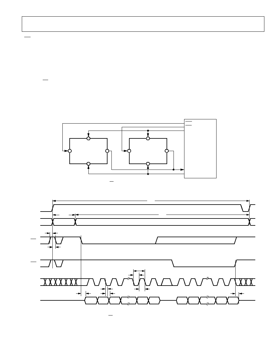
CS MODE 4-WIRE, NO BUSY INDICATOR
This mode is usually used when multiple AD7686s are
connected to an SPI-compatible digital host.
A connection diagram example using two AD7686s is shown in
Figure 37 and the corresponding timing is given in Figure 38.
With SDI high, a rising edge on CNV initiates a conversion,
selects the CS mode, and forces SDO to high impedance. In this
mode, CNV must be held high during the conversion phase and
the subsequent data readback (if SDI and CNV are low, SDO is
driven low). Prior to the minimum conversion time, SDI could
be used to select other SPI devices, such as analog multiplexers,
but SDI must be returned high before the minimum conversion
time and held high until the maximum conversion time to
avoid the generation of the BUSY signal indicator. When the
conversion is complete, the AD7686 enters the acquisition
phase and powers down. Each ADC result can be read by
bringing low its SDI input which consequently outputs the MSB
onto SDO. The remaining data bits are then clocked by
subsequent SCK falling edges. The data is valid on both SCK
edges. Although the rising edge can be used to capture the data,
a digital host using the SCK falling edge allows a faster reading
rate provided it has an acceptable hold time. After the 16th SCK
falling edge, or when SDI goes high, whichever is earlier, SDO
returns to high impedance and another AD7686 can be read.
DATA IN
CLK
CS1
CONVERT
CS2
DIGITAL HOST
02969-
038
CNV
SCK
SDO
SDI
AD7686
CNV
SCK
SDO
SDI
AD7686
Figure 37. CS Mode 4-Wire, No BUSY Indicator Connection Diagram
SDO
D15
D14
D13
D1
D0
t
DIS
SCK
1
2
3
30
31
32
t
HSDO
t
DSDO
t
EN
CONVERSION
ACQUISITION
t
CONV
t
CYC
t
ACQ
ACQUISITION
SDI(CS1)
CNV
t
SSDICNV
t
HSDICNV
D1
14
15
t
SCK
t
SCKL
t
SCKH
D0
D15
D14
17
18
16
SDI(CS2)
02969-
039
Figure 38. CS Mode 4-Wire, No BUSY Indicator Serial Interface Timing
AD7686
Rev 0 | Page 20 of 28
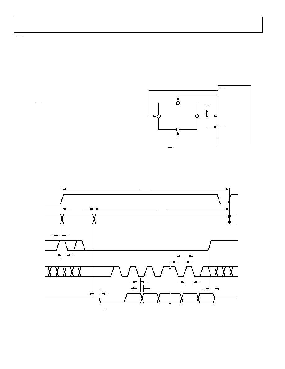
CS MODE 4-WIRE WITH BUSY INDICATOR
This mode is usually used when a single AD7686 is connected
to an SPI-compatible digital host, which has an interrupt input,
and it is desired to keep CNV, which is used to sample the
analog input, independent of the signal used to select the data
reading. This requirement is particularly important in
applications where low jitter on CNV is desired.
The connection diagram is shown in Figure 39 and the
corresponding timing is given in Figure 40.
With SDI high, a rising edge on CNV initiates a conversion,
selects the CS mode, and forces SDO to high impedance. In this
mode, CNV must be held high during the conversion phase and
the subsequent data readback (if SDI and CNV are low, SDO is
driven low). Prior to the minimum conversion time, SDI could
be used to select other SPI devices, such as analog multiplexers,
but SDI must be returned low before the minimum conversion
time and held low until the maximum conversion time to
guarantee the generation of the BUSY signal indicator. When
the conversion is complete, SDO goes from high impedance to
low. With a pull-up on the SDO line, this transition can be used
as an interrupt signal to initiate the data readback controlled by
the digital host. The AD7686 then enters the acquisition phase
and powers down. The data bits are then clocked out, MSB first,
by subsequent SCK falling edges. The data is valid on both SCK
edges. Although the rising edge can be used to capture the data,
a digital host using the SCK falling edge allows a faster reading
rate provided it has an acceptable hold time. After the optional
17th SCK falling edge, or SDI going high, whichever is earlier,
the SDO returns to high impedance.
DATA IN
IRQ
CLK
CONVERT
CS1
VIO
DIGITAL HOST
02969-
040
47k
CNV
SCK
SDO
SDI
AD7686
Figure 39. CS Mode 4-Wire with BUSY Indicator Connection Diagram
SDO
D15
D14
D1
D0
t
DIS
SCK
1
2
3
15
16
17
t
SCK
t
SCKL
t
SCKH
t
HSDO
t
DSDO
t
EN
CONVERSION
ACQUISITION
t
CONV
t
CYC
t
ACQ
ACQUISITION
SDI
CNV
t
SSDICNV
t
HSDICNV
02969-
041
Figure 40. CS Mode 4-Wire with BUSY Indicator Serial Interface Timing
AD7686
Rev 0 | Page 21 of 28
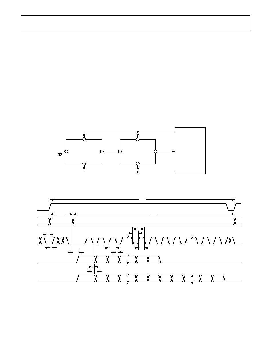
CHAIN MODE, NO BUSY INDICATOR
This mode can be used to daisy-chain multiple AD7686s on a
3-wire serial interface. This feature is useful for reducing
component count and wiring connections, for example, in
isolated multiconverter applications or for systems with a
limited interfacing capacity. Data readback is analogous to
clocking a shift register.
A connection diagram example using two AD7686s is shown in
Figure 41 and the corresponding timing is given in Figure 42.
When SDI and CNV are low, SDO is driven low. With SCK low,
a rising edge on CNV initiates a conversion, selects the chain
mode, and disables the BUSY indicator. In this mode, CNV is
held high during the conversion phase and the subsequent data
readback. When the conversion is complete, the MSB is output
onto SDO and the AD7686 enters the acquisition phase and
powers down. The remaining data bits stored in the internal
shift register are then clocked by subsequent SCK falling edges.
For each ADC, SDI feeds the input of the internal shift register
and is clocked by the SCK falling edge. Each ADC in the chain
outputs its data MSB first, and 16 × N clocks are required to
readback the N ADCs. The data is valid on both SCK edges.
Although the rising edge can be used to capture the data, a
digital host using the SCK falling edge allows a faster reading
rate and consequently more AD7686s in the chain, provided the
digital host has an acceptable hold time. The maximum
conversion rate may be reduced due to the total readback time.
For instance, with a 3 ns digital host set-up time and 3 V
interface, up to four AD7686s running at a conversion rate of
360 kSPS can be daisy-chained on a 3-wire port.
CLK
CONVERT
DATA IN
DIGITAL HOST
02969-
042
CNV
SCK
SDO
SDI
AD7686
B
CNV
SCK
SDO
SDI
AD7686
A
Figure 41. Chain Mode, No BUSY Indicator Connection Diagram
SDO
A
= SDI
B
D
A
15
D
A
14
D
A
13
SCK
1
2
3
30
31
32
t
SSDISCK
t
HSDISC
t
EN
CONVERSION
ACQUISITION
t
CONV
t
CYC
t
ACQ
ACQUISITION
CNV
D
A
1
14
15
t
SCK
t
SCKL
t
SCKH
D
A
0
17
18
16
SDI
A
= 0
SDO
B
D
B
15
D
B
14
D
B
13
D
A
1
D
B
1
D
B
0
D
A
15
D
A
14
t
HSDO
t
DSDO
t
SSCKCNV
t
HSCKCNV
D
A
0
02969-
043
Figure 42. Chain Mode, No BUSY Indicator Serial Interface Timing
AD7686
Rev 0 | Page 22 of 28
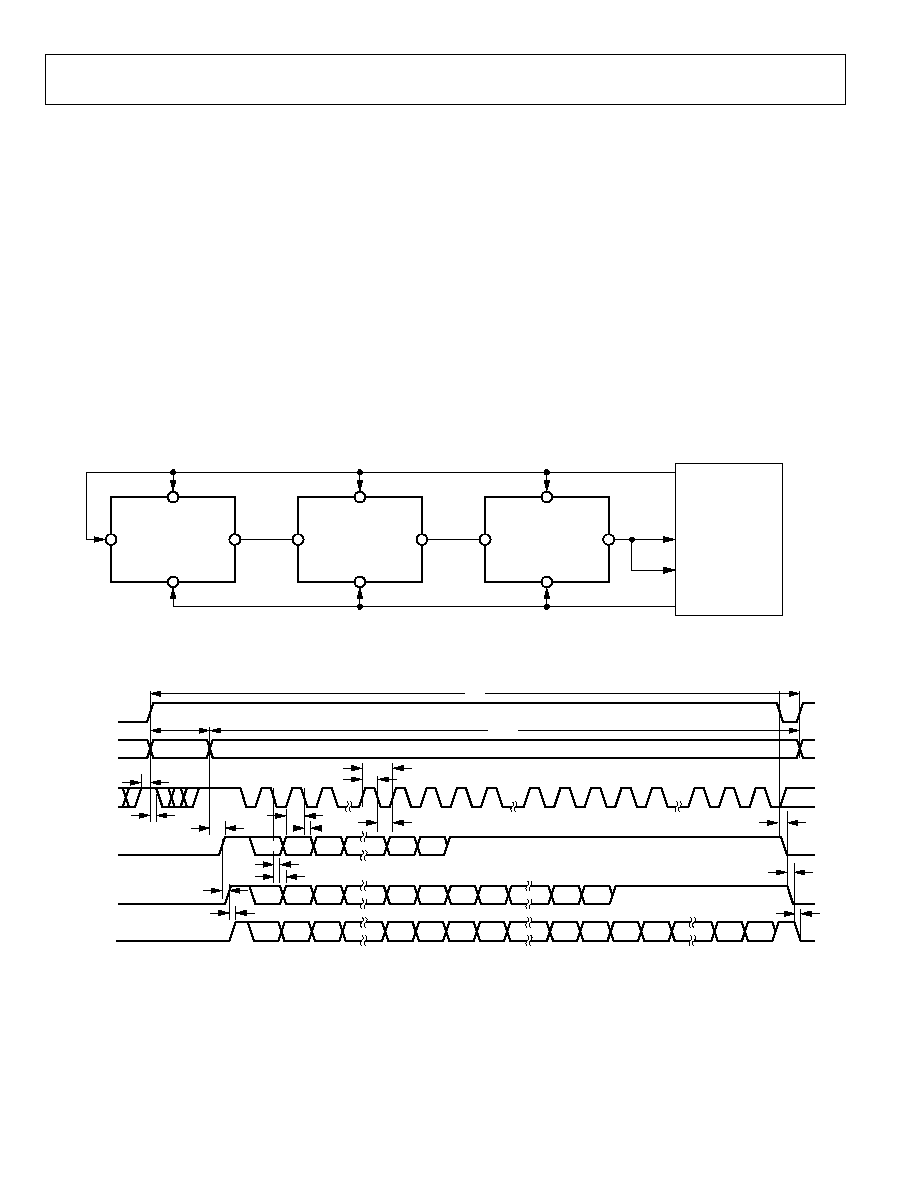
CHAIN MODE WITH BUSY INDICATOR
This mode can also be used to daisy-chain multiple AD7686s
on a 3-wire serial interface while providing a BUSY indicator.
This feature is useful for reducing component count and wiring
connections, for exmpale, in isolated multiconverter
applications or for systems with a limited interfacing capacity.
Data readback is analogous to clocking a shift register.
A connection diagram example using three AD7686s is shown
in Figure 43 and the corresponding timing is given in Figure 44.
When SDI and CNV are low, SDO is driven low. With SCK
high, a rising edge on CNV initiates a conversion, selects the
chain mode, and enables the BUSY indicator feature. In this
mode, CNV is held high during the conversion phase and the
subsequent data readback. When all ADCs in the chain have
completed their conversions, the nearend ADC (ADC C in
Figure 43) SDO is driven high. This transition on SDO can be
used as a BUSY indicator to trigger the data readback controlled
by the digital host. The AD7686 then enters the acquisition
phase and powers down. The data bits stored in the internal
shift register are then clocked out, MSB first, by subsequent
SCK falling edges. For each ADC, SDI feeds the input of the
internal shift register and is clocked by the SCK falling edge.
Each ADC in the chain outputs its data MSB first, and 16 × N +
1 clocks are required to readback the N ADCs. Although the
rising edge can be used to capture the data, a digital host using
the SCK falling edge allows a faster reading rate and
consequently more AD7686s in the chain, provided the digital
host has an acceptable hold time. For instance, with a 3 ns
digital host setup time and 3 V interface, up to four AD7686s
running at a conversion rate of 360 kSPS can be daisy-chained
to a single 3-wire port.
CLK
CONVERT
DATA IN
IRQ
DIGITAL HOST
02969-
044
CNV
SCK
SDO
SDI
AD7686
C
CNV
SCK
SDO
SDI
AD7686
A
CNV
SCK
SDO
SDI
AD7686
B
Figure 43. Chain Mode with BUSY Indicator Connection Diagram
SDO
A
= SDI
B
D
A
15 D
A
14 D
A
13
SCK
1
2
3
35
47
48
t
EN
CONVERSION
ACQUISITION
t
CONV
t
CYC
t
ACQ
ACQUISITION
CNV = SDI
A
D
A
1
4
15
t
SCK
t
SCKH
t
SCKL
D
A
0
17
34
16
SDO
B
= SDI
C
D
B
15 D
B
14 D
B
13
D
A
1
D
B
1
D
B
0 D
A
15 D
A
14
49
t
SSDISCK
t
HSDISC
t
HSDO
t
DSDO
SDO
C
D
C
15 D
C
14 D
C
13
D
A
1
D
A
0
D
C
1
D
C
0
D
A
14
19
31
32
18
33
D
B
1
D
B
0 D
A
15
D
B
15 D
B
14
t
DSDOSDI
t
SSCKCNV
t
HSCKCNV
02969-045
D
A
0
t
DSDOSDI
t
DSDOSDI
t
DSDOSDI
t
DSDOSDI
Figure 44. Chain Mode with BUSY Indicator Serial Interface Timing
AD7686
Rev 0 | Page 23 of 28
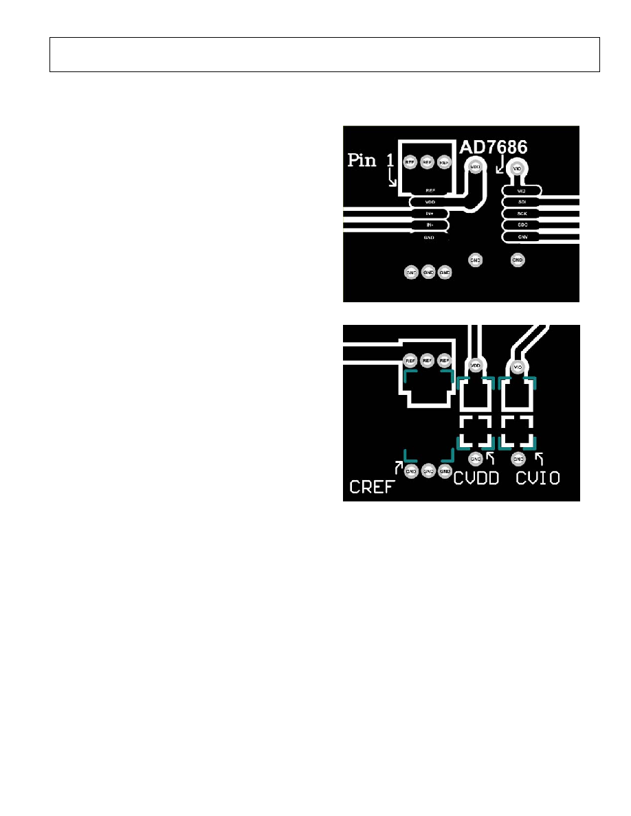
APPLICATION HINTS
LAYOUT
The printed circuit board that houses the AD7686 should be
designed so that the analog and digital sections are separated
and confined to certain areas of the board. The pinout of the
AD7686, with all its analog signals on the left side and all its
digital signals on the right side, eases this task.
Avoid running digital lines under the device because these
couple noise onto the die, unless a ground plane under the
AD7686 is used as a shield. Fast switching signals, such as CNV
or clocks, should never run near analog signal paths. Crossover
of digital and analog signals should be avoided
At least one ground plane should be used. It could be common
or split between the digital and analog sections. In the latter
case, the planes should be joined underneath the AD7686s.
The AD7686 voltage reference input REF has a dynamic input
impedance and should be decoupled with minimal parasitic
inductances. This is done by placing the reference decoupling
ceramic capacitor close to, and ideally right up against, the REF
and GND pins and connecting it with wide, low impedance
traces.
Finally, the power supplies VDD and VIO of the AD7686
should be decoupled with ceramic capacitors (typically 100 nF)
placed close to the AD7686 and connected using short and wide
traces to provide low impedance paths and reduce the effect of
glitches on the power supply lines.
An example of layout following these rules is shown in
Figure 45 and Figure 46.
EVALUATING THE AD7686'S PERFORMANCE
Other recommended layouts for the AD7686 are outlined
in the documentation of the evaluation board for the AD7686
(
EVAL-AD7686
). The evaluation board package includes a fully
assembled and tested evaluation board, documentation, and
software for controlling the board from a PC via the
EVAL-CONTROL BRD3
.
02969-046
Figure 45. Example of Layout of the AD7686 (Top Layer)
02969-047
Figure 46. Example of Layout of the AD7686 (Bottom Layer)
AD7686
Rev 0 | Page 24 of 28
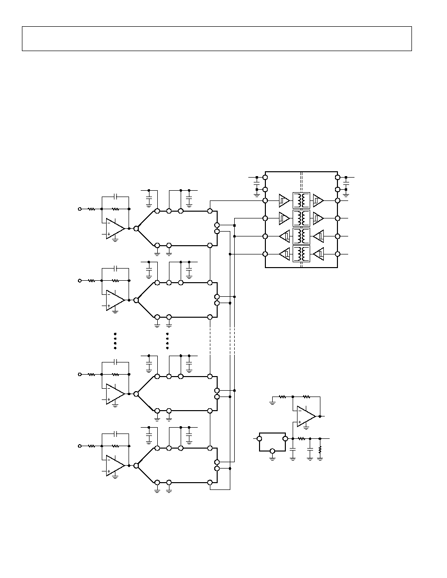
TRUE 16-BIT ISOLATED APPLICATION EXAMPLE
In applications where high accuracy and isolation are required, for
example, power monitoring, motor control, and some medical
equipment, the circuit given in Figure 47, using the AD7686 and the
ADuM1402C digital isolator, provides a compact and high
performance solution.
Multiple AD7686s are daisy-chained to reduce the number of signals
to isolate. Note that the SCKOUT, which is a readback of the
AD7686's clock, has a very short skew with the DATA signal. This
skew is the channel-to-channel matching propagation delay of the
digital isolator (t
PSKCD
). This allows running the serial
interface at the maximum speed of the digital isolator
(45 Mbits/s for the ADuM1402C), which would have been
otherwise limited by the cascade of the propagation delays of
the digital isolator. For instance, four AD7686s running at
330 kSPS can be chained together.
The complete analog chain runs on a 5 V single supply using
the ADR391 low dropout reference voltage and the rail-to-
rail CMOS AD8618 amplifier while offering true bipolar
input range.
IN GND
REF VDD VIO
SDO
V
DD1
, V
E1
GND
1
V
DD2
, V
E2
GND
2
SCK
CNV
SDI
AD7686
1/4 AD8618
5V
1k
2V REF
±10V INPUT
5V REF
5V
5V
10
µ
F
100nF
100nF
IN GND
REF VDD VIO
SDO
SCK
CNV
SDI
AD7686
1/4 AD8618
5V
1k
2V REF
±10V INPUT
5V REF
5V
10
µ
F
100nF
IN GND
REF VDD VIO
SDO
SCK
CNV
SDI
AD7686
1/4 AD8618
5V
1k
2V REF
±10V INPUT
5V REF
5V
10
µ
F
100nF
IN
IN+
IN+
IN+
IN+
GND
REF VDD VIO
SDO
SCK
CNV
SDI
AD7686
1/4 AD8618
5V
1k
4k
4k
4k
4k
2V REF
5V
5V
1k
1k
1k
100nF
10
µ
F
5V REF
2V REF
4k
±10V INPUT
5V REF
5V
10
µ
F
100nF
VIA
VIB
VOC
VOD
VOA
VOB
VIC
VID
2.7V TO 5V
100nF
DATA
SCKOUT
SCKIN
CONVERT
ADuM1402C
OUT
GND
IN
ADR391
02969-
048
Figure 47. A True 16-Bit Isolated Simultaneous Sampling Acquisition System
AD7686
Rev 0 | Page 25 of 28
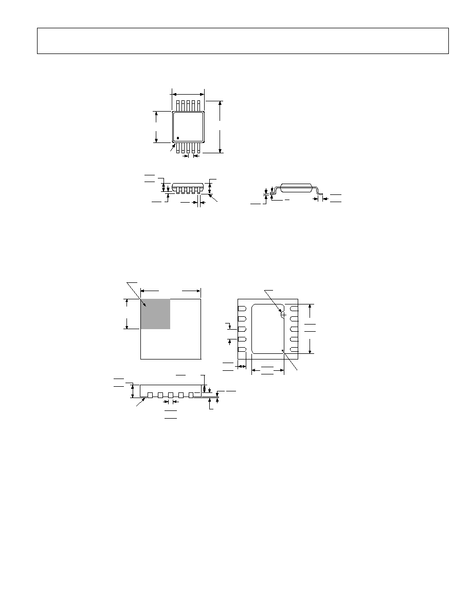
OUTLINE DIMENSIONS
0.23
0.08
0.80
0.60
0.40
8°
0°
0.15
0.00
0.27
0.17
0.95
0.85
0.75
SEATING
PLANE
1.10 MAX
10
6
5
1
0.50 BSC
3.00 BSC
3.00 BSC
4.90 BSC
PIN 1
COPLANARITY
0.10
COMPLIANT TO JEDEC STANDARDS MO-187-BA
Figure 48.10-Lead Mini Small Outline Package [MSOP]
(RM-10)
Dimensions shown in millimeters
3.00
BSC SQ
INDEX
AREA
TOP VIEW
1.50
BCS SQ
EXPOSED
PAD
(BOTTOM VIEW)
1.74
1.64
1.49
2.48
2.38
2.23
1
6
10
0.50
BSC
0.50
0.40
0.30
5
PIN 1
INDICATOR
0.80
0.75
0.70
0.05 MAX
0.02 NOM
SEATING
PLANE
0.30
0.23
0.18
0.20 REF
0.80 MAX
0.55 TYP
SIDE VIEW
PADDLE CONNECTED TO GND.
THIS CONNECTION IS NOT
REQUIRED TO MEET THE
ELECTRICAL PERFORMANCES
Figure 49. 10-Lead Lead Frame Chip Scale Package [QFN
1
(LFCSP_WD)]
3 mm × 3 mm Body, Very Very Thin, Dual Lead
(CP-10-9)
Dimensions shown in millimeters
1
QFN package in development. Contact sales for samples and availability.
AD7686
Rev 0 | Page 26 of 28
ORDERING GUIDE
Model
Integral
Nonlinearity
Temperature Range
Transport Media,
Quantity
Package
Description
Package
Option
Branding
AD7686BRM
±3 LSB max
40°C to +85°C
Tube, 50
10-Lead MSOP
RM-10
C02
AD7686BRMRL7
±3 LSB max
40°C to +85°C
Reel, 1,000
10-Lead MSOP
RM-10
C02
AD7686CRM
±2 LSB max
40°C to +85°C
Tube, 50
10-Lead MSOP
RM-10
C2G
AD7686CRMRL7
±2 LSB max
40°C to +85°C
Reel, 1,000
10-Lead MSOP
RM-10
C2G
EVAL-AD7686CB
1
Evaluation Board
EVAL-CONTROL BRD2
2
Controller Board
EVAL-CONTROL BRD3
2
Controller Board
1
This board can be used as a standalone evaluation board or in conjunction with the EVAL-CONTROL BRDx for evaluation/demonstration purposes.
2
These boards allow a PC to control and communicate with all Analog Devices evaluation boards ending in the CB designators.

AD7686
Rev 0 | Page 27 of 28
NOTES

AD7686
Rev 0 | Page 28 of 28
NOTES
©2005 Analog Devices, Inc. All rights reserved. Trademarks and
registered trademarks are the property of their respective owners.
D0296904/05(0)
Document Outline