 | ÐлекÑÑоннÑй компоненÑ: AD7798 | СкаÑаÑÑ:  PDF PDF  ZIP ZIP |
Äîêóìåíòàöèÿ è îïèñàíèÿ www.docs.chipfind.ru
Low Power, 24-Bit/16-Bit
Sigma-Delta ADC with In-Amp
Preliminary Technical Data
AD7798/AD7799
Rev. PrD.
Information furnished by Analog Devices is believed to be accurate and reliable.
However, no responsibility is assumed by Analog Devices for its use, nor for any
infringements of patents or other rights of third parties that may result from its use.
Specifications subject to change without notice. No license is granted by implication
or otherwise under any patent or patent rights of Analog Devices. Trademarks and
registered trademarks are the property of their respective companies.
One Technology Way, P.O. Box 9106, Norwood, MA 02062-9106, U.S.A.
Tel: 781.329.4700
www.analog.com
Fax: 781.326.8703
© 2004 Analog Devices, Inc. All rights reserved.
FEATURES
Resolution: AD7798:
16-Bit
AD7799: 24-Bit
Three Differential Analog Inputs
Low Noise Programmable Gain Amp
RMS noise: 80 nV (Gain = 64) at 16.6 Hz update rate (AD7798)
65 nV (Gain = 64) at 16.6 Hz update rate (AD7799)
30 nV (Gain = 64) at 4 Hz update rate (AD7799)
Update Rate: 4 Hz to 500 Hz
Power
Supply: 2.7 V to 5.25 V operation
Normal: 330 µA typ (AD7798)
400 µA typ (AD7799)
Power-down: 1 µA max
Simultaneous 50 Hz/60 Hz Rejection
Two Programmable Digital Outputs
Internal Clock Oscillator
Reference Detect
100 nA Burnout Currents
Low Side Power Switch
Independent Interface Power Supply
16-Lead TSSOP
INTERFACE
3-wire serial
SPI®, QSPITM, MICROWIRETM, and DSP compatible
Schmitt trigger on SCLK
APPLICATIONS
Pressure measurement
Weigh scales
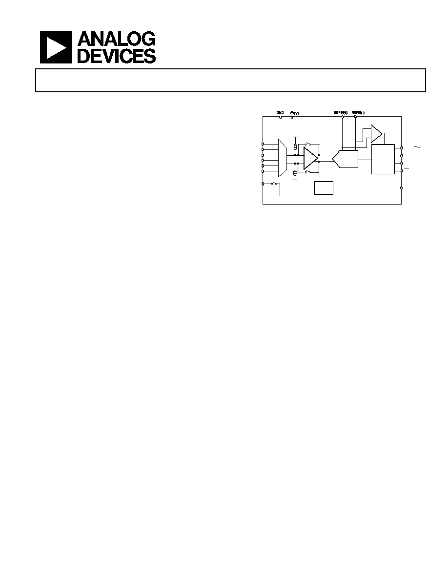
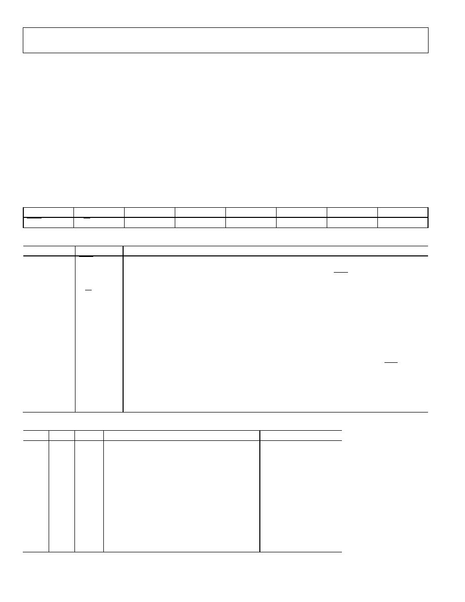
FUNCTIONAL BLOCK DIAGRAM
AD7799/AD7798
SERIAL
INTERFACE
AND
CONTROL
LOGIC
INTERNAL
CLOCK
SIGMA DELTA
ADC
AIN1(-)
AIN2(-)
MUX
IN-AMP
DOUT/RDY
DIN
SCLK
CS
DVDD
AVDD
GND
REFERENCE
DETECT
GND
AIN1(+)
PWRSW
AIN2(+)
AIN3(-)/P2
AIN3(+)/P1
Figure 1.
GENERAL DESCRIPTION
The AD7798/AD7799 is a low power, complete analog front end
for low frequency measurement applications. The device
contains a low noise 24-bit (AD7799)/ 16-bit (AD7798) -
ADC with three differential inputs. The on-chip low noise
instrumentation amplifier means that signals of small
amplitude can be interfaced directly to the ADC. With a gain
setting of 64, the rms noise is 80 nV for AD7798 and 65 nV for
the AD7799 at 16.6 Hz.
T
he device contains a low side power switch which is useful in
bridge applications. The switch allows the bridge to be
disconnected from the power supply when conversions are not
being performed and this will minimise power consumption.
The device also has 100 nA burnout currents. These currents
are used to detect if sensors connected to the analog inputs are
burnt out. Other on-chip features include an internal clock so
the user does not have to supply a clock to the device. This
reduces the component count in a system and provides board
space savings. The update rate is programmable on the
AD7798/99. It can be varied from 4 Hz to 500 Hz.
The part operates with a single power supply from 2.7 V to 5.25
V. It consumes a current of 380 uA maximum for the AD7798
and 450 uA maximum for the AD7799. The AD7799/AD7798 is
housed in a 16-lead TSSOP package.

AD7798/AD7799
Preliminary Technical Data
REV. PrD. Page 2 of 17
TABLE OF CONTENTS
AD7799/AD7798--Specifications.................................................. 3
Timing Characteristics
,
.................................................................... 6
Absolute Maximum Ratings............................................................ 8
Pin Configuration and Function Descriptions............................. 9
Typical Performance Characteristics ........................................... 11
On-chip Registers ........................................................................... 12
Communications Register (RS2, RS1, RS0 = 0, 0, 0) .............. 12
Status Register (RS2, RS1, RS0 = 0, 0, 0; Power-on/Reset =
0x88)............................................................................................. 13
Mode Register (RS2, RS1, RS0 = 0, 0, 1; Power-on/Reset =
0x000A)........................................................................................ 13
Configuration Register (rs2, RS1, RS0 = 0, 1, 0; Power-
on/Reset = 0x0710) .................................................................... 15
Data Register (RS2, RS1, RS0 = 0, 1, 1; Power-on/Reset =
0x0000 (AD7798)/ 0x000000 (AD7799))................................ 16
ID Register (RS2, RS1, RS0 = 1, 0, 0; Power-on/Reset = 0xX8
(AD7798)/ 0xX9 (AD7799))..................................................... 16
OFFSET Register (RS2, RS1, RS0 = 1, 1, 0; Power-on/Reset =
0x8000 (AD7798)/0x800000 (AD7799))................................. 17
FULLSCALE Register (RS2, RS1, RS0 = 1, 1, 1; Power-
on/Reset = 0x5XXX (AD7798)/0x5XXX000 (AD7799)) ..... 17
TYPICAL APPLICATION........................................................ 17
REVISION HISTORY
Prelim D, June 2004: Initial Version

Preliminary Technical Data
AD7798/AD7799
REV. PrD. Page 3 of 17
AD7799/AD7798--SPECIFICATIONS
1
Table 1. (AV
DD
= 2.7 V to 5.25 V; DV
DD
= 2.7 V to 5.25 V; GND = 0 V; REFIN(+) = 2.5 V; REFIN(-) = 0 V; all specifications T
MIN
to
T
MAX
, unless otherwise noted.)
Parameter AD7798/AD7799B
Unit Test
Conditions/Comments
ADC CHANNEL SPECIFICATION
Output Update Rate
4
Hz min nom
500
Hz max nom
ADC CHANNEL
No Missing Codes
2
24
16
Bits min
Bits min
AD7799, f
ADC
125 Hz
AD7798
Resolution
16
Bits p-p
Gain = 128, 16.6 Hz Update Rate
19
16
18.5
Bits p-p
Bits p-p
Bits p-p
Gain = 1, 16.6 Hz Update Rate, AD7799
Gain = 1, 16.6 Hz Update Rate, AD7798
Gain = 64, 4 Hz Update Rate, AD7799
Output Noise and Update Rates
See Tables in ADC
Description
Integral Nonlinearity
±15
ppm of FSR max
3.5 ppm typ, Gain 1 to 32
Offset Error
3
±25
±3
ppm of FSR max
µV typ
Gain = 64 or 128
Offset Error Drift vs. Temperature
4
±10 nV/°C
typ
Full-Scale Error
5
±10 µV
typ
Gain Drift vs. Temperature
4
±0.5
ppm/°C typ
Gain = 1, 2
±3
ppm/°C typ
Gain = 4 to 128
Power Supply Rejection
90
dB min
100 dB typ, AIN = 50 % of full scale
ANALOG INPUTS
Differential Input Voltage Ranges
±REFIN/Gain
V nom
REFIN = REFIN(+) REFIN(), Gain = 1 to 128
Absolute AIN Voltage Limits
2
Unbuffered Mode
Buffered Mode
In-Amp Enabled
GND + 30 mV
AV
DD
30 mV
GND + 100 mV
AV
DD
100 mV
GND + 300 mV
V
DD
1.2
V max
V min
V min
V max
V min
V max
Gain = 1 or 2
Gain = 1 or 2
Gain = 4 to 128
Common Mode Voltage
In-Amp Enabled
Analog Input Current
Buffered Mode or In-Amp Enabled
0.5
V min
Gain = 4 to 128
Average Input Current
2
±200
±1
pA max
nA max
AIN1(+) AIN1(-), AIN2(+) AIN2(-) only.
AIN3(+) AIN3(-).
Average Input Current Drift
±2
pA/°C typ
Unbuffered Mode
Average Input Current
±400
nA/V typ
Gain = 1 or 2
Input current varies with input voltage.
Average Input Current Drift
Normal Mode Rejection
2
@ 50 Hz, 60 Hz
±50
70
pA/V/°C typ
dB min
73 dB typ, 50 ± 1 Hz, 60 ± 1 Hz, FS[3:0] = 1010
6
@ 50 Hz
84
dB min
90 dB typ, 50 ± 1 Hz, FS[3:0] = 1001
6
@ 60 Hz
90
dB min
90 dB typ, 60 ± 1 Hz, FS[3:0] = 1000
6
Common Mode Rejection
@DC
@ 50 Hz, 60 Hz
2
90
100
dB min
dB min
AIN = 50% of FS
80 dB typ, FS[3:0] = 1010
6
50 ± 1 Hz (FS[3:0] = 1001
6
), 60 ± 1 Hz (FS[3:0] =
1000
6
)

AD7798/AD7799
Preliminary Technical Data
REV. PrD. Page 4 of 17
Parameter AD7798/AD7799B
Unit Test
Conditions/Comments
REFERENCE INPUT
REFIN Voltage
2.5
V nom
REFIN = REFIN(+) REFIN()
Reference Voltage Range
2
Absolute REFIN Voltage Limits
2
0.1
AV
DD
GND 30 mV
V min
V max
V min
AV
DD
+ 30 mV
V max
Average reference Input Current
400
nA/V typ
Average Reference Input Current Drift
±0.03
nA/V/°C typ
Normal Mode Rejection
2
See ANALOG INPUTS
Common Mode Rejection
See ANALOG INPUTS
Reference Detect
0.3
0.65
V min
V max
NOREF bit Inactive if VREF < 0.3 V
NOREF bit Active if VREF > 0.65 V
LOW SIDE POWER SWITCH
R
ON
Allowable Current
5
7
20
max
max
mA max
AV
DD
= 5V
AV
DD
= 3V
Continuous Current
INTERNAL CLOCK
Drift
64 ±2%
0.01
KHz nom
%/°C typ
LOGIC INPUTS
All Inputs Except SCLK and DIN
V
INL
, Input Low Voltage
0.8
V max
DV
DD
= 5 V
0.4
V max
DV
DD
= 3 V
V
INH
, Input High Voltage
2.0
V min
DV
DD
= 3 V or 5 V
SCLK and DIN Only (Schmitt-
Triggered Input)
2
V
T
(+)
1.4/2
V min/V max
DV
DD
= 5 V
V
T
()
0.8/1.4
V min/V max
DV
DD
= 5 V
V
T
(+) V
T
()
0.3/0.85
V min/V max
DV
DD
= 5 V
V
T
(+)
0.9/2
V min/V max
DV
DD
= 3 V
V
T
()
0.4/1.1
V min/V max
DV
DD
= 3 V
V
T
(+) - V
T
()
Input Currents
Input Capacitance
0.3/0.85
±1
10
V min/V max
µA max
pF typ
DV
DD
= 3 V
V
IN
= DV
DD
or GND
All Digital Inputs
LOGIC OUTPUTS
V
OH
, Output High Voltage
2
DV
DD
0.6
V min
DV
DD
= 3 V, I
SOURCE
= 100 µA
V
OL
, Output Low Voltage
2
0.4
V
max
DV
DD
= 3 V, I
SINK
= 100 µA
V
OH
, Output High Voltage
2
4
V min
DV
DD
= 5 V, I
SOURCE
= 200 µA
V
OL
, Output Low Voltage
2
0.4
V
max
DV
DD
= 5 V, I
SINK
= 1.6 mA
Floating-State Leakage Current
±1
µA max
Floating-State Output Capacitance
10
pF typ
Data Output Coding
Offset Binary
DIGITAL OUTPUTS
P1 and P2
V
OH
, Output High Voltage
2
V
OL
, Output Low Voltage
2
V
OH
, Output High Voltage
2
V
OL
, Output Low Voltage
2
AV
DD
0.6
0.4
4
0.4
V min
V max
V min
V max
AV
DD
= 3 V, I
SOURCE
= 100 µA
AV
DD
= 3 V, I
SINK
= 100 µA
AV
DD
= 5 V, I
SOURCE
= 200 µA
AV
DD
= 5 V, I
SINK
= 800 µA

Preliminary Technical Data
AD7798/AD7799
REV. PrD. Page 5 of 17
Parameter AD7798/AD7799B
Unit Test
Conditions/Comments
SYSTEM CALIBRATION
2
Full-Scale Calibration Limit
Zero-Scale Calibration Limit
Input Span
1.05 x FS
-1.05 x FS
0.8 x FS
2.1 x FS
V max
V min
V min
V max
POWER REQUIREMENTS
7
Power Supply Voltage
V
DD
GND
IOV
DD
GND
2.7/5.25
2.7/5.25
V min/max
V min/max
Power Supply Currents
I
DD
Current
150
µA max
125 µA typ, Unbuffered Mode
175
µA max
150 µA typ, Buffered Mode, In-Amp Bypassed
380
450
µA max
µA max
330 µA typ, In-Amp used (AD7798)
400 µA typ, IN-AMP used (AD7799)
I
DD
(Power-Down Mode)
1
µA max
1
Temperature Range 40°C to +105°C.
2
Specification is not production tested but is supported by characterization data at initial product release.
3
A System calibration will reduce this error to the order of the noise for the programmed gain and update rate.
4
A calibration at any temperature will remove this error.
5
Full-scale error applies to both positive and negative full-scale and applies at the factory calibration conditions (AV
DD
= 4 V).
6
FS[3:0] are the four bits used in the mode register to select the output word rate.
7
Digital inputs equal to DV
DD
or GND.
AD7798/AD7799
Preliminary Technical Data
REV. PrD. Page 6 of 17
TIMING CHARACTERISTICS
8, 9
Table 2. (AV
DD
= 2.7 V to 5.25 V; DV
DD
= 2.7 V to 5.25; GND = 0 V, Input Logic 0 = 0 V, Input Logic 1 = DV
DD
, unless otherwise
noted.)
Parameter
Limit at T
MIN
, T
MAX
(B Version)
Unit Conditions/Comments
t
3
100
ns min
SCLK High Pulsewidth
t
4
100
ns min
SCLK Low Pulsewidth
Read Operation
t
1
0
ns min
CS Falling Edge to DOUT/RDY Active Time
60
ns max
DV
DD
= 4.75 V to 5.25 V
80
ns max
DV
DD
= 2.7 V to 3.6 V
t
2
10
0
ns min
SCLK Active Edge to Data Valid Delay
11
60
ns max
DV
DD
= 4.75 V to 5.25 V
80
ns max
DV
DD
= 2.7 V to 3.6 V
t
5
12, 13
10
ns min
Bus Relinquish Time after CS Inactive Edge
80
ns max
t
6
100
ns max
SCLK Inactive Edge to CS Inactive Edge
t
7
10
ns min
SCLK Inactive Edge to DOUT/RDY High
Write Operation
t
8
0
ns min
CS Falling Edge to SCLK Active Edge Setup Time
11
t
9
30
ns min
Data Valid to SCLK Edge Setup Time
t
10
25
ns min
Data Valid to SCLK Edge Hold Time
t
11
0
ns min
CS Rising Edge to SCLK Edge Hold Time
8
Sample tested during initial release to ensure compliance. All input signals are specified with t
R
= t
F
= 5 ns (10% to 90% of V
DD
) and timed from a voltage level of 1.6 V.
9
See
and
.
Figure 3
Figure 4
10
These numbers are measured with the load circuit of
Figure 2
Figure 2
and defined as the time required for the output to cross the V
OL
or V
OH
limits.
11
SCLK active edge is falling edge of SCLK.
12
These numbers are derived from the measured time taken by the data output to change 0.5 V when loaded with the circuit of
. The measured number is then
extrapolated back to remove the effects of charging or discharging the 50 pF capacitor. This means that the times quoted in the timing characteristics are the true bus
relinquish times of the part and, as such, are independent of external bus loading capacitances.
13
RDY returns high after a read of the ADC. In single conversion mode and continuous conversion mode, the same data can be read again, if required, while RDY is high,
although care should be taken to ensure that subsequent reads do not occur close to the next output update. In continuous read mode, the digital word can be read
only once.
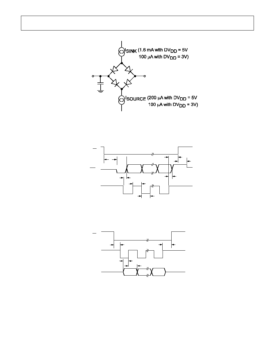
Preliminary Technical Data
AD7798/AD7799
REV. PrD. Page 7 of 17
TO OUTPUT PIN
+1.6 V
50 pF
Figure 2. Load Circuit for Timing Characterization
t
2
t
3
t
4
t
1
t
6
t
5
t
7
04227-0-003
CS (I)
DOUT/RDY (O)
SCLK (I)
I = INPUT, O = OUTPUT
MSB
LSB
Figure 3. Read Cycle Timing Diagram
04227-0-004
I = INPUT, O = OUTPUT
CS (I)
SCLK (I)
DIN (I)
MSB
LSB
t
8
t
9
t
10
t
11
Figure 4. Write Cycle Timing Diagram

AD7798/AD7799
Preliminary Technical Data
REV. PrD. Page 8 of 17
ABSOLUTE MAXIMUM RATINGS
Table 3. (T
A
= 25°C, unless otherwise noted.)
Parameter Rating
AV
DD
to GND
DV
DD
to GND
-0.3V to +7V
-0.3V to +7V
Analog Input Voltage to GND
0.3 V to AV
DD
+ 0.3 V
Reference Input Voltage to GND
0.3 V to AV
DD
+ 0.3 V
Digital Input Voltage to GND
0.3 V to DV
DD
+ 0.3 V
Digital Output Voltage to GND
AIN/digital Input Current
0.3 V to DV
DD
+ 0.3 V
10 mA
Operating Temperature Range
40°C to +105°C
Storage Temperature Range
65°C to +150°C
Maximum Junction Temperature
150°C
TSSOP
JA
Thermal Impedance
97.9°C/W
JC
Thermal Impedance
14°C/W
Lead Temperature, Soldering
Vapor Phase (60 sec)
Infrared
215°C
220°C
Stresses above those listed under Absolute Maximum Ratings
may cause permanent damage to the device. This is a stress
rating only; functional operation of the device at these or any
other conditions above those listed in the operational sections
of this specification is not implied. Exposure to absolute
maximum rating conditions for extended periods may affect
device reliability.
Preliminary Technical Data
AD7798/AD7799
REV. PrD. Page 9 of 17
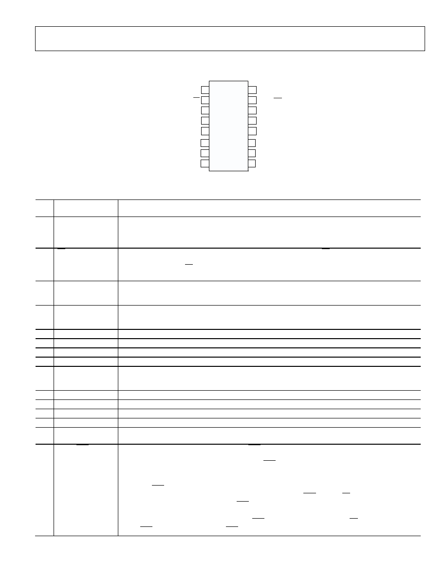
PIN CONFIGURATION AND FUNCTION DESCRIPTIONS
3
4
5
14
13
12
D VD D
AVD D
GND
1
2
16
15
D I N
D OU T /RD Y
6
7
8
11
10
9
PWRSW
AD 7799/98
T OP VI EW
(Not To Scale)
REFI N(- )
REFI N(+)
AI N3(+)/P1
AI N3(- )/P2
AI N1(+)
SCLK
CS
AI N1(- )
AI N2(+)
AI N2(- )
Figure 5. Pin Configuration
Table 4. Pin Function Descriptions
Pin
No.
Mnemonic
Function
1 SCLK
Serial Clock Input for Data Transfers to and from the ADC. The SCLK has a Schmitt-triggered input, making
the interface suitable for opto-isolated applications. The serial clock can be continuous with all data
transmitted in a continuous train of pulses. Alternatively, it can be a noncontinuous clock with the
information being transmitted to or from the ADC in smaller batches of data.
2
CS
Chip Select Input. This is an active low logic input used to select the ADC. CS can be used to select the ADC
in systems with more than one device on the serial bus or as a frame synchronization signal in communi-
cating with the device. CS can be hardwired low, allowing the ADC to operate in 3-wire mode with SCLK,
DIN, and DOUT used to interface with the device.
3 AIN3(+)/P1
Analog Input/Digital Output pin. AIN3(+) is the positive terminal of the differential analog input pair
AIN3(+)/AIN3(-). Alternatively, this pin can function as a general purpose output bit referenced between
AV
DD
and GND
4 AIN3()/P2
Analog Input/ Digital Output pin. AIN3() is the negative terminal of the differential analog input pair
AIN3(+)/AIN3(-). Alternatively, this pin can function as a general purpose output bit referenced between
AV
DD
and GND
5
AIN1(+)
Analog Input. AIN1(+) is the positive terminal of the differential analog input pair AIN1(+)/AIN1(-).
6
AIN1(-)
Analog Input. AIN1() is the negative terminal of the differential analog input pair AIN1(+)/AIN1(-).
7
AIN2(+)
Analog Input. AIN2(+) is the positive terminal of the differential analog input pair AIN2(+)/AIN2(-).
8
AIN2(-)
Analog Input. AIN2() is the negative terminal of the differential analog input pair AIN2(+)/AIN2(-).
9 REFIN(+)
Positive Reference Input. REFIN(+) can lie anywhere between AV
DD
and GND + 0.1 V.
The nominal reference voltage (REFIN(+) REFIN()) is 2.5 V, but the part functions with a reference from 0.1
V to AV
DD
.
10
REFIN(-)
Negative Reference Input. This reference input can lie anywhere between GND and AV
DD
0.1 V.
11
PSW
Low Side Power Switch to GND.
12
GND
Ground Reference Point.
13 AV
DD
Supply Voltage, 2.7 V to 5.25 V.
14 DV
DD
Serial Interface Supply voltage, 2.7 V to 5 V. DV
DD
is independent of AV
DD
, therefore the serial interface can
be operated at 3V with V
DD
at 5V or vice versa.
15
DOUT/RDY
Serial Data Output/Data Ready Output. DOUT/RDY serves a dual purpose . It functions as a serial data output
pin to access the output shift register of the ADC. The output shift register can contain data from any of the
on-chip data or control registers. In addition, DOUT/RDY operates as a data ready pin,
going low to indicate the completion of a conversion. If the data is not read after the conversion, the pin will
go high before the next update occurs.
The DOUT/RDY falling edge can be used as an interrupt to a processor, indicating that valid data is available.
With an external serial clock, the data can be read using the DOUT/RDY pin. With CS low, the data/control
word informa-tion is placed on the DOUT/RDY pin on the SCLK falling edge and is valid on the SCLK rising
edge.
The end of a conversion is also indicated by the RDY bit in the status register. When CS is high, the
DOUT/RDY pin is three-stated but the RDY bit remains active.

AD7798/AD7799
Preliminary Technical Data
REV. PrD. Page 10 of 17
Pin
No.
Mnemonic
Function
16 DIN
Serial Data Input to the Input Shift Register on the ADC. Data in this shift register is transferred to the control
registers within the ADC, the register selection bits of the communications register identifying the
appropriate register.

Preliminary Technical Data
AD7798/AD7799
REV. PrD. Page 11 of 17
TYPICAL PERFORMANCE CHARACTERISTICS
Figure 6.
Figure 7.
Figure 8.
Figure 9.
Figure 10.
Figure 11.
AD7798/AD7799
Preliminary Technical Data
REV. PrD. Page 12 of 17
ON-CHIP REGISTERS
The ADC is controlled and configured via a number of on-chip registers, which are described on the following pages. In the following
descriptions, set implies a Logic 1 state and cleared implies a Logic 0 state, unless otherwise stated.
COMMUNICATIONS REGISTER (RS2, RS1, RS0 = 0, 0, 0)
The communications register is an 8-bit write-only register. All communications to the part must start with a write operation to the com-
munications register. The data written to the communications register determines whether the next operation is a read or write operation,
and to which register this operation takes place. For read or write operations, once the subsequent read or write operation to the selected
register is complete, the interface returns to where it expects a write operation to the communications register. This is the default state of
the interface and, on power-up or after a reset, the ADC is in this default state waiting for a write operation to the communications regis-
ter. In situations where the interface sequence is lost, a write operation of at least 32 serial clock cycles with DIN high returns the ADC to
this default state by resetting the entire part. Table 5 outlines the bit designations for the communications register. CR0 through CR7 indi-
cate the bit location, CR denoting the bits are in the communications register. CR7 denotes the first bit of the data stream. The number in
brackets indicates the power-on/reset default status of that bit.
CR7 CR6 CR5 CR4 CR3 CR2 CR1 CR0
WEN(0) R/W(0)
RS2(0)
RS1(0)
RS0(0)
CREAD(0)
0(0)
0(0)
Table 5. Communications Register Bit Designations
Bit Location
Bit Name
Description
CR7
WEN
Write Enable Bit. A 0 must be written to this bit so that the write to the communications register actually
occurs. If a 1 is the first bit written, the part will not clock on to subsequent bits in the register. It will stay
at this bit location until a 0 is written to this bit. Once a 0 is written to the WEN bit, the next seven bits
will be loaded to the communications register.
CR6
R/W
A 0 in this bit location indicates that the next operation will be a write to a specified register. A 1 in this
position indicates that the next operation will be a read from the designated register.
CR5CR3 RS2RS0 Register Address Bits. These address bits are used to select which of the ADC's registers are being
selected during this serial interface communication. See Table 6.
CR2
CREAD
Continuous Read of the Data Register. When this bit is set to 1 (and the data register is selected), the
serial interface is configured so that the data register can be continuously read, i.e., the contents of the
data register are placed on the DOUT pin automatically when the SCLK pulses are applied. The commu-
nications register does not have to be written to for data reads. To enable continuous read mode, the
instruction 01011100 must be written to the communications register. To exit the continuous read
mode, the instruction 01011000 must be written to the communications register while the RDY pin is
low. While in continuous read mode, the ADC monitors activity on the DIN line so that it can receive the
instruction to exit continuous read mode. Additionally, a reset will occur if 32 consecutive 1s are seen on
DIN. Therefore, DIN should be held low in continuous read mode until an instruction is to be written to
the device.
CR1CR0
0
These bits must be programmed to logic 0 for correct operation.
Table 6. Register Selection
RS2 RS1 RS0 Register
Register
Size
0
0
0
Communications Register during a Write Operation
8-Bit
0
0
0
Status Register during a Read Operation
8-Bit
0 0 1 Mode
Register
16-Bit
0 1 0 Configuration
Register
16-Bit
0
1
1
Data Register
24-Bit (AD7799)
16-bit (AD7798)
1 0 0 ID
Register
8-Bit
1 0 1 IO
Register
8-Bit
1
1
0
Offset Register
24-Bit (AD7799)
16-bit (AD7798)
1
1
1
Full-Scale Register
24-Bit (AD7799)
16-Bit (AD7798)
Preliminary Technical Data
AD7798/AD7799
REV. PrD. Page 13 of 17
STATUS REGISTER (RS2, RS1, RS0 = 0, 0, 0; POWER-ON/RESET = 0x88)
The status register is an 8-bit read-only register. To access the ADC status register, the user must write to the communications register,
select the next operation to be a read, and load bits RS2, RS1 and RS0 with 0. Table 7 outlines the bit designations for the status register.
SR0 through SR7 indicate the bit locations, SR denoting the bits are in the status register. SR7 denotes the first bit of the data stream. The
number in brackets indicates the power-on/reset default status of that bit.
SR7
SR6
SR5
SR4
SR3
SR2
SR1
SR0
RDY(1)
ERR(0)
NOREF(0)
0(0)
0/1
CH2(0)
CH1(0)
CH0(0)
Table 7. Status Register Bit Designations
Bit Location
Bit Name
Description
SR7
RDY
Ready bit for ADC. Cleared when data is written to the ADC data register. The RDY bit is set automatically
after the ADC data register has been read or a period of time before the data register is updated with a
new conversion result to indicate to the user not to read the conversion data. It is also set when the part
is placed in power-down mode. The end of a conversion is indicated by the DOUT/RDY pin also. This pin
can be used as an alternative to the status register for monitoring the ADC for conversion data.
SR6
ERR
ADC Error Bit. This bit is written to at the same time as the RDY bit. Set to indicate that the result written
to the ADC data register has been clamped to all 0s or all 1s. Error sources include overrange,
underrange, NOREF Cleared by a write operation to start a conversion.
SR5 NOREF
No Reference Bit. Set to indicate that one or both of the REFIN pins is floating or the applied voltage is
below a specified threshold. When set, conversion results are clamped to all ones.
Cleared to indicate that a valid reference is applied between REFIN(+) and REFIN(-).
The NOREF bit is enabled by setting the REF_DET bit in the Configuration register to 1. The ERR bit is
also set if the voltage applied to the reference input is invalid.
SR4
0
This bit is automatically cleared.
SR3
0/1
This bit is automatically cleared on the AD7798, and is automatically set on the AD7799.
SR2SR0
CH2CH0
These bits indicate which channel is being converted by the ADC.
MODE REGISTER (RS2, RS1, RS0 = 0, 0, 1; POWER-ON/RESET = 0x000A)
The mode register is a 16-bit register from which data can be read or to which data can be written. This register is used to configure the
Low Side Power Switch, select the mode of the ADC and select the ADC update rate. Table 8 outlines the bit designations for the mode
register. MR0 through MR15 indicate the bit locations, MR denoting the bits are in the mode register. MR15 denotes the first bit of the
data stream. The number in brackets indicates the power-on/reset default status of that bit. Any write to the setup register resets the
modulator and filter and sets the RDY bit.
MR15
MR14
MR13
MR12
MR11
MR10
MR9
MR8
MD2(0)
MD1(0)
MD0(0)
PSW(0)
0(0)
0(0)
0(0)
0(0)
MR7
MR6
MR5
MR4
MR3
MR2
MR1
MR0
(0)
(0)
0(0)
0(0)
FS3(1) FS2(0) FS1(1) FS0(0)
Table 8. Mode Register Bit Designations
Bit Location
Bit Name
Description
MR15MR13
MD2MD0
Mode Select Bits. These bits select the operational mode of the AD7798/AD7799 (See Table 9).
MR12
PSW
Power Switch Control Bit.
Set by user to close the power switch PSW to GND. The power switch can sink up to 20 mA.
Cleared by user to open the power switch.
When the ADC is placed in power-down mode, the power switch is opened.
MR11-MR4
0
These bits must be programmed with a Logic 0 for correct operation.
MR3-MR0
FS3-FS0
Filter Update Rate Select Bits (see Table 10).

AD7798/AD7799
Preliminary Technical Data
REV. PrD. Page 14 of 17
Table 9. Operating Modes
MD2
MD1
MD0
Mode
0
0
0
Continuous Conversion Mode (Default).
In continuous conversion mode, the ADC continuously performs conversions and places the result in the data
register. RDY goes low when a conversion is complete. The user can read these conversions by placing the
device in continuous read mode whereby the conversions are automatically placed on the DOUT line when
SCLK pulses are applied. Alternatively, the user can instruct the ADC to output the conversion by writing to
the communications register. After power-on, or following a write to the Mode, Configuration or IO
Registers, a conversion is available after a period 2/ f
ADC
while subsequent conversions are available at a
frequency of f
ADC
.
0
0
1
Single Conversion Mode.
In single conversion mode, the ADC is placed in power-down mode when conversions are not being
performed. When single conversion mode is selected, the ADC powers up and performs a single conversion,
which occurs after a period 2/f
ADC
. The conversion result in placed in the data register, RDY goes low, and the
ADC returns to power-down mode. The conversion remains in the data register and RDY remains active (low)
until the data is read or another conversion is performed.
0
1
0
Idle Mode.
In Idle Mode, the ADC Filter an Modulator are held in a reset state although the modulator clocks are still
provided
0 1 1
Power-Down
Mode.
In power down mode, all the AD7798/99 circuitry is powered down including the power switch and
burnout currents
.
1
0
0
Internal Zero-Scale Calibration.
An internal short is automatically connected to the enabled channel. A calibration takes 2 conversion cycles
to complete. RDY goes high when the calibration is initiated and returns low when the the calibration is
complete. The ADC is placed in idle mode following a calibration. The measured offset coefficient is placed in
the offset register of the selected channel.
1
0
1
Internal Full-Scale Calibration.
The fullscale input is automatically connected to the selected analog input for this calibration. When the gain
equals 1, a calibration takes 2 conversion cycles to complete. For higher gains, 4 conversion cycles are
required for the fullscale calibration. RDY goes high when the calibration is initiated and returns low when
the calibration is complete. The ADC is placed in idle mode following a calibration. The measured full-scale
calibration coefficient is placed in the fullscale register of the selected channel. A fullscale calibration is
required each time the gain of a channel is changed. The full-scale error of the AD7799/AD7798 is calibrated
in the factory at both a gain of 1 and 128. These values are loaded into the fullscale register when the gain is 1
or 128. If a different PGA gain is used, then an Internal Full-Scale Calibration is required to calibrate out the
gain error associated with that PGA gain. Note that Internal Fullscale Calibrations cannot be performed at a
gain of 128.
1
1
0
System Offset Calibration.
User should connect the system zero-scale input to the channel input pins as selected by the CH2-CH0 bits.
A system offset calibration takes 2 conversion cycles to complete. RDY goes high when the calibration is
initiated and returns low when the calibration is complete. The ADC is placed in idle mode following a
calibration. The measurded offset calibration coefficient is placed in the offset register of the selected
channel.
1
1
1
System Full-Scale Calibration.
User should connect the system full-scale input to the channel input pins s selected by the CH2-CH0 bits. A
system full-scale calibration takes 2 conversion cycles to complete. RDY goes high when the calibration is
initiated and returns low when the calibration is complete. The ADC is placed in idle mode following a
calibration. The measured full-scale calibration coefficient is placed in the fullscale register of the selected
channel.
Preliminary Technical Data
AD7798/AD7799
REV. PrD. Page 15 of 17
Table 10
.
Update Rates Available
FS3
FS2 FS1
FS0 f
ADC
(Hz)
Tsettle
(ms)
Rejection @50 Hz/60 Hz
0
0
0
0
x
x
0
0
0
1
500
5
0
0
1
0
250
8
0
0
1
1
125
16
0
1
0
0
62.5
32
0
1
0
1
50
40
0
1
1
0
41.6
48
0 1 1 1 33.3
60
1
0
0
0
19.6
101
90 dB (60 Hz only)
1
0
0
1
16.6
120
84 dB (50 Hz only)
1
0
1
0
16.6
120
70 dB (50 Hz and 60 Hz)
1
0
1
1
12.5
160
67 dB (50 Hz and 60 Hz)
1
1
0
0
10
200
69 dB (50 Hz and 60 Hz)
1
1
0
1
8.33
240
73 dB (50 Hz and 60 Hz)
1
1
1
0
6.25
320
74 dB (50 Hz and 60 Hz)
1
1
1
1
4.17
480
75 dB @ 50/60 Hz
CONFIGURATION REGISTER (RS2, RS1, RS0 = 0, 1, 0; POWER-ON/RESET = 0x0710)
The configuration register is a 16-bit register from which data can be read or to which data can be written. This register is used to configure
the ADC for unipolar or bipolar mode, enable or disable the buffer, enable or disable the burnout currents, select the gain and select the ana-
log input channel. CON0 through CON15 indicate the bit locations, CON denoting the bits are in the configuration register. CON15
denotes the first bit of the data stream. The number in brackets indicates the power-on/reset default status of that bit.
CON15
CON14 CON13 CON12 CON11
CON10
CON9
CON8
0
0
BO(0)
U/B (0)
0(0)
G2(1)
G1(1)
G0(1)
CON7
CON6
CON5
CON4
CON3
CON2
CON1
CON0
0 0 REF_DET(0)
BUF(1)
0(0)
CH2(0) CH1(0) CH0(0)
Table 11. Configuration Register Bit Designations
Bit Location
Bit Name
Description
CON15CON14
0
These bits must be programmed with a logic 0 for correct operation.
CON13
BO
Burnout Current Enable Bit. When this bit is set to 1 by the user, the 100 nA current sources in the
signal path are enabled. When BO = 0, the burnout currents are disabled. The burnout currents
can be enabled only when the buffer or In-Amp is active.
CON12
U/B
Unipolar/Bipolar Bit. Set by user to enable unipolar coding, i.e., zero differential input will result in
0x0000(00) output and a full-scale differential input will result in 0XFFFF(FF) output for the
AD7798(99).
Cleared by the user to enable bipolar coding. Negative full-scale differential input will result in an
output code of 0x0000(00), zero differential input will result in an output code of 0x8000(00), and
a positive full-scale differential input will result in an output code of 0xFFFF(FF) for the
AD7798(99).
CON11
0
This bit must be programmed with a Logic 0 for correct operation.
CON10-CON8
G2-G0
Gain Select Bits.
Written by the user to select the ADC input range as follows
G2
G1
G0
Gain
ADC Input Range (2.5V Reference)
0 0 0 1 (In-Amp not
used)
±2.5 V
0 0 1 2 (In-Amp not
used)
±1.25 V
AD7798/AD7799
Preliminary Technical Information
REV. PrD. Page 16 of 17
Bit Location
Bit Name
Description
0 1 0 4
±625
mV
0 1 1 8
±312.5
mV
1 0 0 16
±156.2
mV
1 0 1 32
±78.125
mV
1 1 0 64
±39.06
mV
1 1 1 128
±19.53
mV
CON7-CON6
0
These bits must be programmed to a logic 0 for correct operation.
CON5
REF_DET
Enables the Reference Detect Function.
When set, the NOREF bit in the status register indicates when the reference being used by the
ADC is not present.
When cleared, the reference detect function is disabled.
CON4 BUF
Configures the ADC for buffered or unbuffered mode of operation. If cleared, the ADC operates in
unbuffered mode, lowering the power consumption of the device. If set, the ADC operates in
buffered mode, allowing the user to place source impedances on the front end without
contributing gain errors to the system.
CON3
0
This bits must be programmed to a logic 0 for correct operation.
CON2-CON0 CH2-CH0
Channel
Select
bits.
Written by the user to select the active analog input channel to the ADC.
CH2 CH1 CH0 Channel
Calibration
Pair
0 0 0 AIN1(+)
AIN1(-) 0
0 0 1 AIN2(+)
AIN2(-) 1
0 1 0 AIN3(+)
AIN3(-) 2
0 1 1 AIN1(-)
AIN1(-) 0
1 0 0 Reserved
1 0 1 Reserved
1 1 0 Reserved
1 1 1 VDD
Monitor
DATA REGISTER (RS2, RS1, RS0 = 0, 1, 1; POWER-ON/RESET = 0x0000 (AD7798)/ 0X000000 (AD7799))
The conversion result from the ADC is stored in this data register. This is a read-only register. On completion of a read operation from
this register, the RDY bit/pin is set.
ID REGISTER (RS2, RS1, RS0 = 1, 0, 0; POWER-ON/RESET = 0xX8 (AD7798)/ 0xX9 (AD7799))
The Identification Number for the AD7798/AD7799 is stored in the ID register. This is a read-only register.
IO REGISTER (RS2, RS1, RS0 = 1, 0, 1; POWER-ON/RESET = 0x00)
The I/O register is an 8-bit register from which data can be read or to which data can be written. IO0 through IO7 indicate
the bit locations, IO denoting the bits are in the IO register. Table 12 outline the bit designations for the IO register. IO7 denotes the first
bit of the data stream. The number in brackets indicates the power-on/reset default status of that bit.
IO7
IO6 IO5 IO4 IO3 IO2 IO1 IO0
0 IOEN(0)
IO2DAT(0)
IO1DAT(0)
0 0 0 0
Table 12. I/O register Bit Designations
Bit Location
Bit Name
Description
IO7
0
These bits must be programmed to a logic 0 for correct operation.
IO6
IOEN
Configures the pins AIN3(+)/P1 and AIN3(-)/P2 as analog input pins or digital output pins.
When this bit is set, the pins are configured as digital output pins P1 and P2.
When this bit is cleared, these pins are configured as analog input pins AIN3(+) and AIN3(-).
IO5-IO4 IO2DAT/IO1DAT
P2/P1
Data.
IO3-IO0
0
These bits must be programmed to a logic 0 for correct operation.
Preliminary Technical Information
AD7798/AD7799
REV. PrD. Page 17 of 17
OFFSET REGISTER (RS2, RS1, RS0 = 1, 1, 0; Power-on/Reset = 0x8000 (AD7798)/0x800000 (AD7799))
The offset register holds the offset calibration coefficient for the ADC. The power-on-reset value of the internal zero-scale calibration
coefficient register is 8000 hex (AD7798)/800000 hex (AD7799). The AD7798/AD7799 has 3 offset registers. Each of these registers is a
16/24-bit read/write register.
However, when writing to the offset-scale registers, the ADC must be placed in power down mode or idle
mode. This register is used in conjunction with its associated full-scale register to form a register pair. The power-on-reset value is
automatically overwritten if an internal or system zero-scale calibration is initiated by the user.
FULLSCALE Register (RS2, RS1, RS0 = 1, 1, 1; Power-on/Reset = 0x5XXX (AD7798)/0x5XXX000 (AD7799))
The full-scale register holds the full-scale calibration coefficient for the ADC. The AD7798/AD7799 has 3 full-scale registers. Each of
these registers is a 16/24-bit read/write register.
However, when writing to the full-scale registers, the ADC must be placed in power
down mode or idle mode. The full-scale error of the AD7799/AD7798 is calibrated in the factory at both a gain of 1 and 128. Therefore if
the gain is set to 128, as on power-on, or if the gain is set to 1, the factory calibrated internal full-scale coefficients are automatically
loaded into the full-scale registers of the AD7799/AD7798. Therefore, every device will have different default coefficients. The user can
overwrite these values, if required. These coefficients will be automatically overwritten if an internal or system full-scale calibration is
initiated by the user. A full-scale calibration should be performed when the gain is changed. When the gain equals 128, internal full-scale
calibrations cannot be performed.
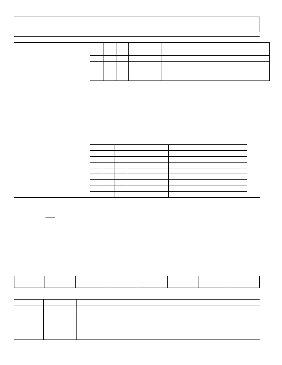
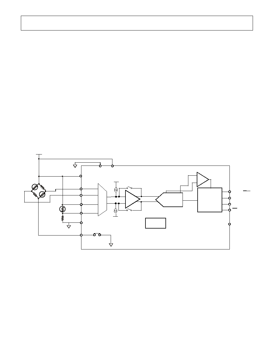
TYPICAL APPLICATION
AVDD
IN+
IN-
OUT+
OUT-
REFIN(-)
GND
AVDD
AD7799/AD7798
SERIAL
INTERFACE
AND
CONTROL
LOGIC
SIGMA DELTA
ADC
REFERENCE
DETECT
INTERNAL
CLOCK
AIN1(+)
AIN1(-)
AIN2(+)
AIN2(-)
MUX
IN-AMP
REFIN(+)
DOUT/RDY
DIN
SCLK
CS
DVDD
AVDD
GND
PWRSW
Figure 12.
PR04856-0-6/04(PrD)
Document Outline