 | ÐлекÑÑоннÑй компоненÑ: AD8106 | СкаÑаÑÑ:  PDF PDF  ZIP ZIP |
AD8106/AD8107 260 MHz, 16 × 5 Buffered Video Crosspoint Switches Data Sheet (Rev. 0)
260 MHz, 16 × 5 Buffered
Video Crosspoint Switches
AD8106/AD8107
Rev. 0
Information furnished by Analog Devices is believed to be accurate and reliable. However, no
responsibility is assumed by Analog Devices for its use, nor for any infringements of patents or other
rights of third parties that may result from its use. Specifications subject to change without notice. No
license is granted by implication or otherwise under any patent or patent rights of Analog Devices.
Trademarks and registered trademarks are the property of their respective owners.
One Technology Way, P.O. Box 9106, Norwood, MA 02062-9106, U.S.A.
Tel: 781.329.4700
www.analog.com
Fax: 781.461.3113
©2006 Analog Devices, Inc. All rights reserved.
FEATURES
16 × 5 high speed, nonblocking switch arrays
AD8106: G = 1, AD8107: G = 2
Pin compatible with
AD8110
/
AD8111
, 16 × 8 switch arrays
For a 16 × 16 array, see
AD8114
/
AD8115
For a 16 x 8 array, see
AD8110
/
AD8111
Complete solution
Buffered inputs
Five output amplifiers
Drives 150
loads
Excellent video performance
60 MHz 0.1 dB gain flatness
0.02% differential gain error (R
L
= 150
)
0.028 differential phase error (R
L
= 150
)
Excellent ac performance
-3 dB bandwidth > 260 MHz
500 V/
s slew rate
Low power of 50 mA
Low all-hostile crosstalk of -78 dB @ 5 MHz
Output disable allows connection of multiple device outputs
Reset pin allows disabling of all outputs
Excellent ESD rating: Exceeds 4000 V human body model
80-lead LQFP (12 mm × 12 mm)
APPLICATIONS
Routing of high speed signals including:
Composite video (NTSC, PAL, S, SECAM)
Component video (YUV, RGB)
Compressed video (MPEG, Wavelet)
3-level digital video (HDB3)
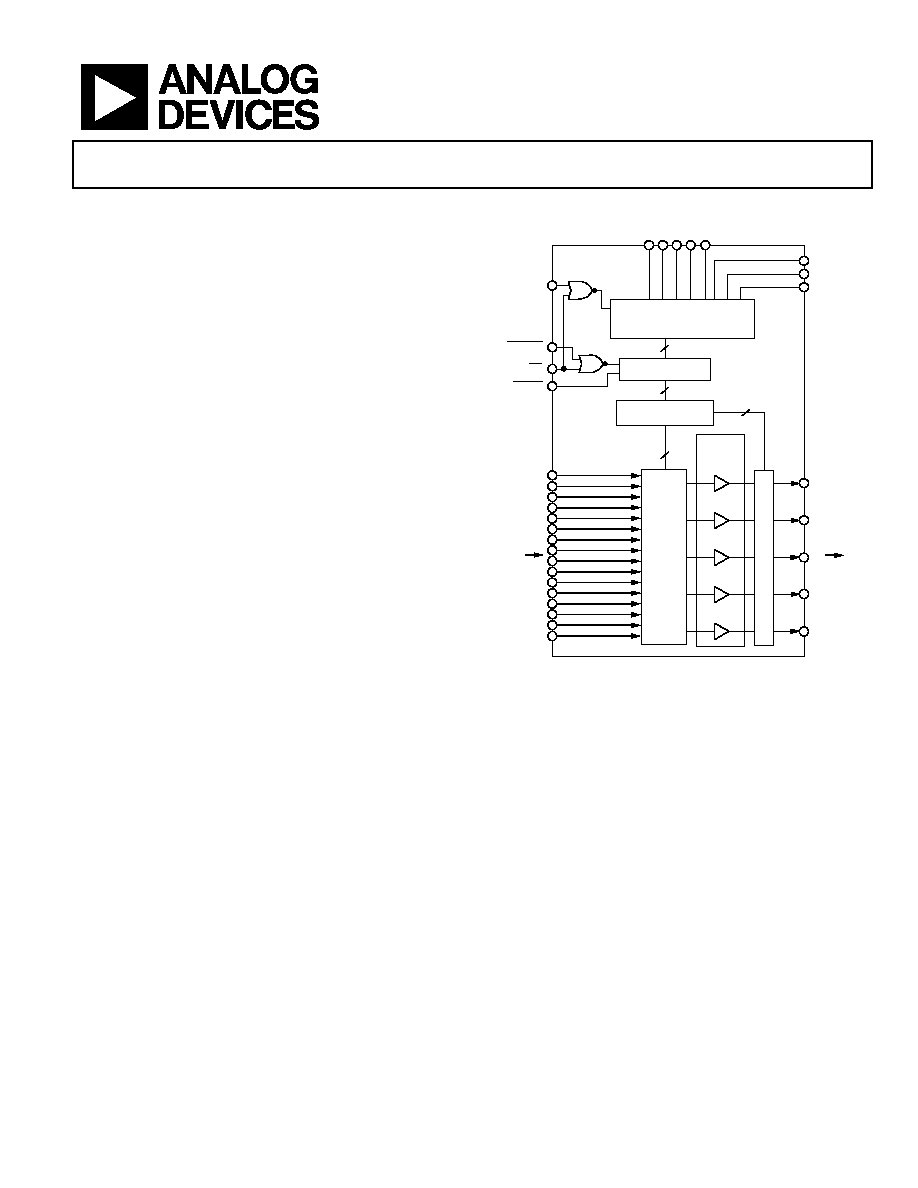
FUNCTIONAL BLOCK DIAGRAM
AD8106/AD8107
OUTPUT
BUFFER
G = 1,
G = 2
25
25
80
25-BIT REGISTER
(RANK 1)
PARALLEL LATCH
(RANK 2)
DECODE
5 × 5:16 DECODERS
5
CLK
UPDATE
CE
RESET
16 INPUTS
A0
5 OUTPUTS
SET INDIVIDUAL
OR RESET ALL
OUTPUTS
TO OFF
A1
A2
D0 D1 D2 D3 D4
057
74-
00
1
EN
A
B
L
E
/D
IS
A
B
LE
SWITCH
MATRIX
Figure 1.
GENERAL DESCRIPTION
The AD8106 and AD8107 are high speed, 16 × 5 video crosspoint
switch matrices. They offer a -3 dB signal bandwidth greater
than 260 MHz, and channel switch times of less than 25 ns
with 1% settling. With -78 dB of crosstalk and
-
97 dB isolation
(@ 5 MHz), the AD8106/AD8107 are useful in many high speed
applications. The differential gain and differential phase of
greater than 0.02% and 0.02° respectively, along with 0.1 dB
flatness out to 60 MHz, make the AD8106/AD8107 ideal for
video signal switching.
The AD8106 and AD8107 include five independent output
buffers that can be placed into a high impedance state for parallel-
ing crosspoint outputs, preventing off channels from loading the
output bus. The AD8106 has a gain of 1, while the AD8107
offers a gain of 2. Both operate on voltage supplies of ±5 V while
consuming only 30 mA of idle current. The channel switching is
performed via a parallel control, allowing updating of an
individual output without reprogramming the entire array.
The AD8106/AD8107 are offered in an 80-lead LQFP and are
available over the extended industrial temperature range of
-40°C to +85°C.

AD8106/AD8107
Rev. 0 | Page 2 of 28
TABLE OF CONTENTS
Features .............................................................................................. 1
Applications....................................................................................... 1
Functional Block Diagram .............................................................. 1
General Description ......................................................................... 1
Revision History ............................................................................... 2
Specifications..................................................................................... 3
Timing Characteristics ................................................................ 5
Absolute Maximum Ratings............................................................ 6
Maximum Power Dissipation ..................................................... 6
ESD Caution.................................................................................. 6
Pin Configuration and Function Descriptions............................. 8
I/O Schematics .................................................................................. 9
Typical Performance Characteristics ........................................... 10
Theory of Operation ...................................................................... 16
Power-On Reset.......................................................................... 16
Initialization ................................................................................ 16
Gain Selection............................................................................. 16
Creating Larger Crosspoint Arrays.......................................... 16
Crosstalk ...................................................................................... 18
PCB Layout ................................................................................. 19
Evaluation Board ............................................................................ 21
Controlling the Evaluation Board from a PC......................... 25
Data-Line Overshoot on Printer Ports .................................... 25
Outline Dimensions ....................................................................... 27
Ordering Guide .......................................................................... 27
REVISION HISTORY
3/06--Revision 0: Initial Version

AD8106/AD8107
Rev. 0 | Page 3 of 28
SPECIFICATIONS
V
S
= ±5 V, T
A
= 25°C, R
L
= 1 k, unless otherwise noted.
Table 1.
Parameter
Conditions
Min
Typ
Max
Unit
Reference
DYNAMIC PERFORMANCE
-3 dB Bandwidth
200 mV p-p, R
L
= 150
300/190
390/260
MHz
Figure 10, Figure 16
2 V p-p, R
L
= 150
150
MHz
Figure 10, Figure 16
Propagation Delay
2 V p-p, R
L
= 150
5
ns
Slew Rate
2 V step, R
L
= 150
500
V/s
Settling Time
0.1%, 2 V step, R
L
= 150
40
ns
Figure 15, Figure 21
Gain Flatness
0.05 dB, 200 mV p-p, R
L
= 150
60/40
MHz
Figure 10, Figure 16
0.05 dB, 2 V p-p, R
L
= 150
65/40
MHz
Figure 10, Figure 16
0.1 dB, 200 mV p-p, R
L
= 150
80/57
MHz
Figure 10, Figure 16
0.1 dB, 2 V p-p, R
L
= 150
70/57
MHz
Figure 10, Figure 16
NOISE/DISTORTION PERFORMANCE
Differential Gain Error
NTSC or PAL, R
L
= 1 k
0.01
%
NTSC or PAL, R
L
= 150
0.02
%
Differential Phase Error
NTSC or PAL, R
L
= 1 k
0.01
Degrees
NTSC or PAL, R
L
= 150
0.02
Degrees
Crosstalk, All Hostile
f = 5 MHz
78/85
dB
Figure 11, Figure 17
f = 10 MHz
70/80
dB
Figure 11, Figure 17
Off Isolation, Input/Output
f = 10 MHz, R
L
= 150 , one channel
93/99
dB
Figure 26, Figure 32
Input Voltage Noise
0.01 MHz to 50 MHz
15
nV/Hz
Figure 23, Figure 29
DC PERFORMANCE
Gain Error
R
L
= 1 k
0.04/0.1
0.07/0.5 %
R
L
= 150
0.15/0.25
%
Gain Matching
No load, channel-to-channel
0.02/1.0 %
R
L
= 1 k, channel-to-channel
0.09/1.0 %
Gain Temperature Coefficient
0.5/8
ppm/°C
OUTPUT CHARACTERISTICS
Output Impedance
DC, enabled
0.2
Figure 27, Figure 33
Disabled
10/0.001
M
Figure 24, Figure 30
Output Disable Capacitance
Disabled
2
pF
Output Leakage Current
Disabled, AD8106 only
1/NA
A
Output Voltage Range
No load
±2.5
±3
V
Output Current
20
40
mA
Short-Circuit Current
65
mA
INPUT CHARACTERISTICS
Input Offset Voltage
Worst case (all configurations)
5
20
mV
Figure 38, Figure 44
Temperature coefficient
12
V/°C
Figure 39, Figure 45
Input Voltage Range
±2.5/±1.25
±3/±1.5
V
Input Capacitance
Any switch configuration
2.5
pF
Input Resistance
1
10
M
Input Bias Current
Per output selected
2
5
A
SWITCHING CHARACTERISTICS
Enable On Time
60
ns
Switching Time, 2 V Step
50% UPDATE to 1% settling
25
ns
Switching Transient (Glitch)
Measured at output
20/30
mV p-p
Figure 25, Figure 31

AD8106/AD8107
Rev. 0 | Page 4 of 28
Parameter
Conditions
Min
Typ
Max
Unit
Reference
POWER SUPPLIES
Supply Current
AVCC, outputs enabled, no load
30
mA
AVCC, outputs disabled
15
mA
AVEE, outputs enabled, no load
30
mA
AVEE, outputs disabled
15
mA
DVCC
11
mA
Supply Voltage Range
±4.5 to ±5.5
V
PSRR
f = 100 kHz
75/78
dB
Figure 22, Figure 28
f = 1 MHz
-55/-58
dB
OPERATING TEMPERATURE
Temperature Range
Operating (still air)
-40 to +85
°C
JA
Operating (still air)
48
°C/W
AD8106/AD8107
Rev. 0 | Page 5 of 28
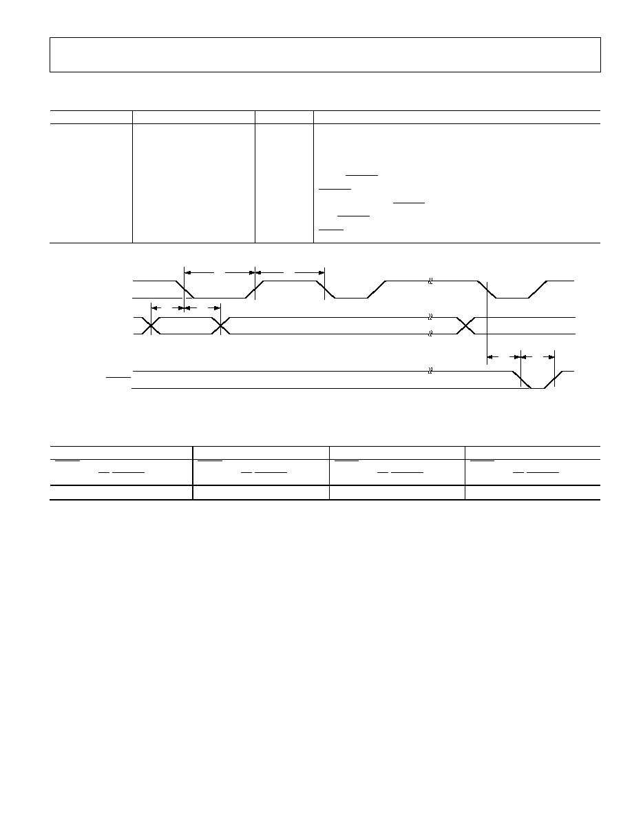
TIMING CHARACTERISTICS
Table 2.
Parameter Limit
at
T
MIN
, T
Unit Description
MAX
t
1
20
ns min
Data setup time
t
100
ns min
CLK pulse width
2
t
20
ns min
Data hold time
3
t
100
ns min
CLK pulse separation
4
t
5
0
ns min
CLK to UPDATE delay
t
6
50
ns min
UPDATE pulse width
8
ns
max
Propagation delay, UPDATE to switch on or off
100
ns
max
CLK, UPDATE rise and fall times
200
ns min
RESET time
1
0
1
0
1 = LATCHED
CLK
D0 TO D4
A0 TO A2
0 = TRANSPARENT
UPDATE
t
5
t
6
t
2
t
1
t
3
t
4
05
77
4-
00
2
Figure 2. Timing Diagram
Table 3. Logic Levels
V
IH
V
I
IL
IH
I
IL
RESET, CLK, D0, D1, D2, D3, D4,
A0, A1, A2, CE, UPDATE
RESET, CLK, D0, D1, D2, D3, D4,
A0, A1, A2, CE, UPDATE
RESET, CLK, D0, D1, D2, D3, D4,
A0, A1, A2,
RESET, CLK, D0, D1, D2, D3, D4,
A0, A1, A2,
CE, UPDATE
CE, UPDATE
2.0 V min
0.8 V max
20 A max
-400 A min
AD8106/AD8107
Rev. 0 | Page 6 of 28
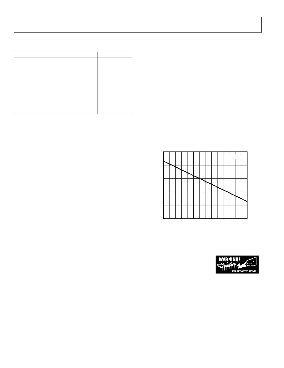
ABSOLUTE MAXIMUM RATINGS
Table 4.
MAXIMUM POWER DISSIPATION
Parameter
Rating
The maximum power that can be safely dissipated by the
AD8106/AD8107 is limited by the associated rise in junction
temperature. The maximum safe junction temperature for
plastic encapsulated devices is determined by the glass
transition temperature of the plastic, approximately 150°C.
Temporarily exceeding this limit can cause a shift in parametric
performance due to a change in the stresses exerted on the die
by the package.
Supply Voltage
12.0 V
Internal Power Dissipation
AD8106/AD8107 80-Lead LQFP (ST-80-1)
2.6 W
Input Voltage
±V
S
Output Short-Circuit Duration
Observe power
derating curves
JA
48°C/W
Operating Temperature Range
-40°C to 85°C
Storage Temperature Range
-65°C to +125°C
Exceeding a junction temperature of 175°C for an extended
period can result in device failure.
Lead Temperature (Soldering 10 sec)
300°C
Stresses above those listed under Absolute Maximum Ratings
may cause permanent damage to the device. This is a stress
rating only; functional operation of the device at these or any
other conditions above those indicated in the operational
section of this specification is not implied. Exposure to absolute
maximum rating conditions for extended periods may affect
device reliability.
While the AD8106/AD8107 is internally short-circuit
protected, this may not be sufficient to guarantee that the
maximum junction temperature (150°C) is not exceeded under
all conditions. To ensure proper operation, it is necessary to
observe the maximum power derating curves shown in Figure 3.
AMBIENT TEMPERATURE (°C)
5
MA
XI
MU
M
PO
W
E
R
D
I
S
S
I
P
A
TI
O
N
(
W
)
4
0
50
80
40 30 20 10 0
10 20 30 40 50 60 70
3
2
1
90
T
J
= 150°C
05
77
4-
0
03
Figure 3. Maximum Power Dissipation vs. Temperature
ESD CAUTION
ESD (electrostatic discharge) sensitive device. Electrostatic charges as high as 4000 V readily accumulate on
the human body and test equipment and can discharge without detection. Although this product features
proprietary ESD protection circuitry, permanent damage may occur on devices subjected to high energy
electrostatic discharges. Therefore, proper ESD precautions are recommended to avoid performance
degradation or loss of functionality.
AD8106/AD8107
Rev. 0 | Page 7 of 28
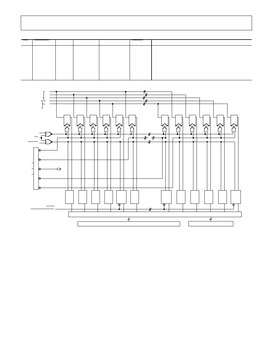
Table 5. Operation Truth Table
CE
UPDATE
CLK
DATA IN
DATA OUT
RESET
Operation/Comment
1
X
X
X
X
X
No change in logic.
0
1
1
f
D0 ... D4
A0 ... A2
NA in parallel
mode
The data on the parallel data lines, D0 to D4, are loaded into
the 40-bit serial shift register location addressed by A0 to A2.
0
0
X
X
X
1
Data in the 40-bit shift register transfers into the parallel
latches that control the switch array. Latches are transparent.
X
X
X
X
X
0
Asynchronous operation. All outputs are disabled.
Remainder of logic is unchanged.
D
CLK
Q
3
T
O
5 DE
CO
DE
R
A0
A1
A2
CLK
CE
UPDATE
5
80
(OUTPUT
ENABLE)
PARALLEL
DATA
D1
D2
D3
OUTPUT ENABLE
SWITCH MATRIX
D0
D4
05
77
4-
004
D
LE
OUT0
B0
Q
D
CLK
Q
D
LE
OUT0
B1
Q
D
CLK
Q
D
LE
OUT0
B2
Q
D
CLK
Q
D
LE
OUT0
B3
Q
D
CLK
Q
D
LE
OUT1
B0
Q
D
CLK
Q
D
LE
OUT3
EN
Q
CLR
D
CLK
Q
D
LE
OUT4
B0
Q
D
CLK
Q
D
LE
OUT4
B1
Q
D
CLK
Q
D
LE
OUT4
B2
Q
D
CLK
Q
D
LE
OUT4
B3
Q
OUT0 EN
OUT1 EN
OUT2 EN
OUT3 EN
OUT4 EN
RESET
(OUTPUT DISABLE)
D
CLK
Q
D
LE
OUT0
EN
Q
CLR
D
CLK
Q
D
LE
OUT4
EN
CLR
DECODE
Q
Figure 4. Logic Diagram
AD8106/AD8107
Rev. 0 | Page 8 of 28
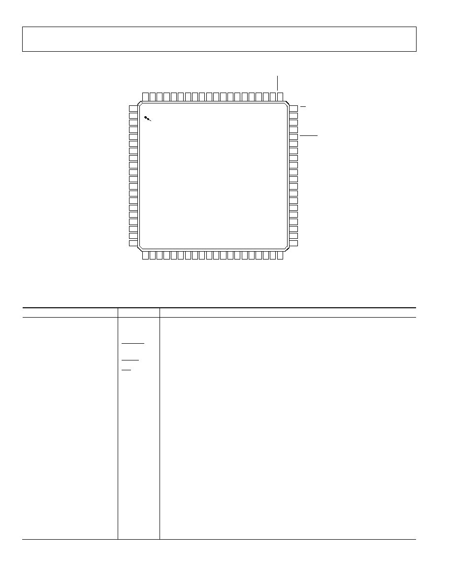
PIN CONFIGURATION AND FUNCTION DESCRIPTIONS
80
79
78
77
76
75
74
73
72
71
70
69
68
67
66
65
64
63
62
61
56
57
58
59
54
55
52
53
50
51
60
45
46
47
48
43
44
42
49
41
5
4
3
2
7
6
9
8
1
11
10
16
15
14
13
18
17
20
19
12
40
39
38
37
35
34
33
32
31
30
29
28
27
26
25
24
23
22
21
36
DG
ND
DV
CC
IN
0
7
AG
ND
IN
0
6
AG
ND
IN
0
5
AG
ND
IN
0
4
AG
N
D
IN
0
3
AG
N
D
IN
0
2
AG
ND
IN
0
1
AG
ND
IN
0
0
DV
C
C
DG
N
D
RE
S
E
T
AG
N
D
AV
E
E
NC
AG
N
D
AV
C
C
NC
AG
N
D
AV
E
E
0
4
OU
T0
4
AG
ND
0
4
A
V
C
C03/
0
4
OU
T0
3
AG
ND
0
3
A
V
E
E
02/
03
OU
T0
2
AG
ND
0
2
A
V
C
C01/
0
2
OU
T0
1
AG
ND
0
1
CE
RESERVED
CLK
RESERVED
UPDATE
RESERVED
A0
A1
A2
D0
D1
D2
D3
D4
AGND
AVEE
AVCC
AVCC00
AGND00
OUT00
IN08
AGND
IN09
AGND
IN10
AGND
IN11
AGND
IN12
AGND
IN13
AGND
IN14
AGND
IN15
AGND
AVEE
AVCC
AVCC
NC
A
V
E
E
00/
01
AD8106/AD8107
16 × 5
80L LQFP
(12mm × 12mm)
TOP VIEW
(PINS DOWN)
0.5mm LEAD PITCH
05
77
4-
01
0
PIN 1
INDICATOR
Figure 5. 80-Lead Plastic LQFP
Table 6. Pin Function Descriptions
Pin No.
Mnemonic
Description
INxx
Analog Inputs; xx = Channel Numbers 00 through 15.
64 , 66, 68, 70, 72, 74, 76, 78, 1,
3, 5, 7, 9, 11, 13, 15,
58
CLK
Clock, TTL Compatible. Falling edge triggered.
56
UPDATE
Enable (Transparent) Low. Allows serial register to connect directly to switch matrix. Data
latched when high.
61
RESET
Disable Outputs, Active Low.
60
CE
Chip Enable, Enable Low. Must be low to clock in and latch data.
41, 38, 35, 32, 29
OUTyy
Analog Outputs; yy = Channel Numbers 00 Through 04.
AGND
Analog Ground for Inputs and Switch Matrix.
2, 4, 6, 8, 10, 12, 14, 16, 21, 24, 27,
46, 65, 67, 69, 71, 73, 75, 77
63, 79
DVCC
5 V for Digital Circuitry.
62, 80
DGND
Ground for Digital Circuitry.
17, 22, 45
AVEE
-5 V for Inputs and Switch Matrix.
18, 19, 25, 44
AVCC
+5 V for Inputs and Switch Matrix.
42, 39, 36, 33, 30
AGNDxx
Ground for Output Amp; xx = Output Channel Numbers 00 Through 07. Must be connected.
43, 37, 31, 22
AVCCxx/yy
+5 V for Output Amplifier. Shared by channel numbers xx and yy. Must be connected.
40, 34, 28
AVEExx/yy
-5 V for Output Amplifier. Shared by channel numbers xx and yy. Must be connected.
54
A0
Parallel Data Input, TTL Compatible (Output Select LSB).
53
A1
Parallel Data Input, TTL Compatible (Output Select).
52
A2
Parallel Data Input, TTL Compatible (Output Select MSB).
51
D0
Parallel Data Input, TTL Compatible (Input Select LSB).
50
D1
Parallel Data Input, TTL Compatible (Input Select).
49
D2
Parallel Data Input, TTL Compatible (Input Select).
48
D3
Parallel Data Input, TTL Compatible (Input Select MSB).
47
D4
Parallel Data Input, TTL Compatible (Output Enable).
AD8106/AD8107
Rev. 0 | Page 9 of 28
I/O SCHEMATICS
ESD
ESD
INPUT
V
CC
AV
EE
05
774
-
005
ESD
ESD
DGND
RESET
V
CC
20k
057
74
-
0
07
RESET
Figure 8.
Input
Figure 6. Analog Input
ESD
ESD
INPUT
V
CC
DGND
05
774
-
008
ESD
ESD
AV
EE
V
CC
OUTPUT
1k
(AD8107 ONLY)
05
774
-
006
Figure 9. Logic Input
Figure 7. Analog Output
AD8106/AD8107
Rev. 0 | Page 10 of 28
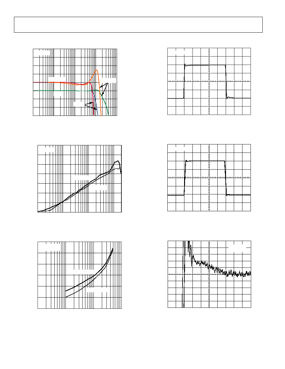
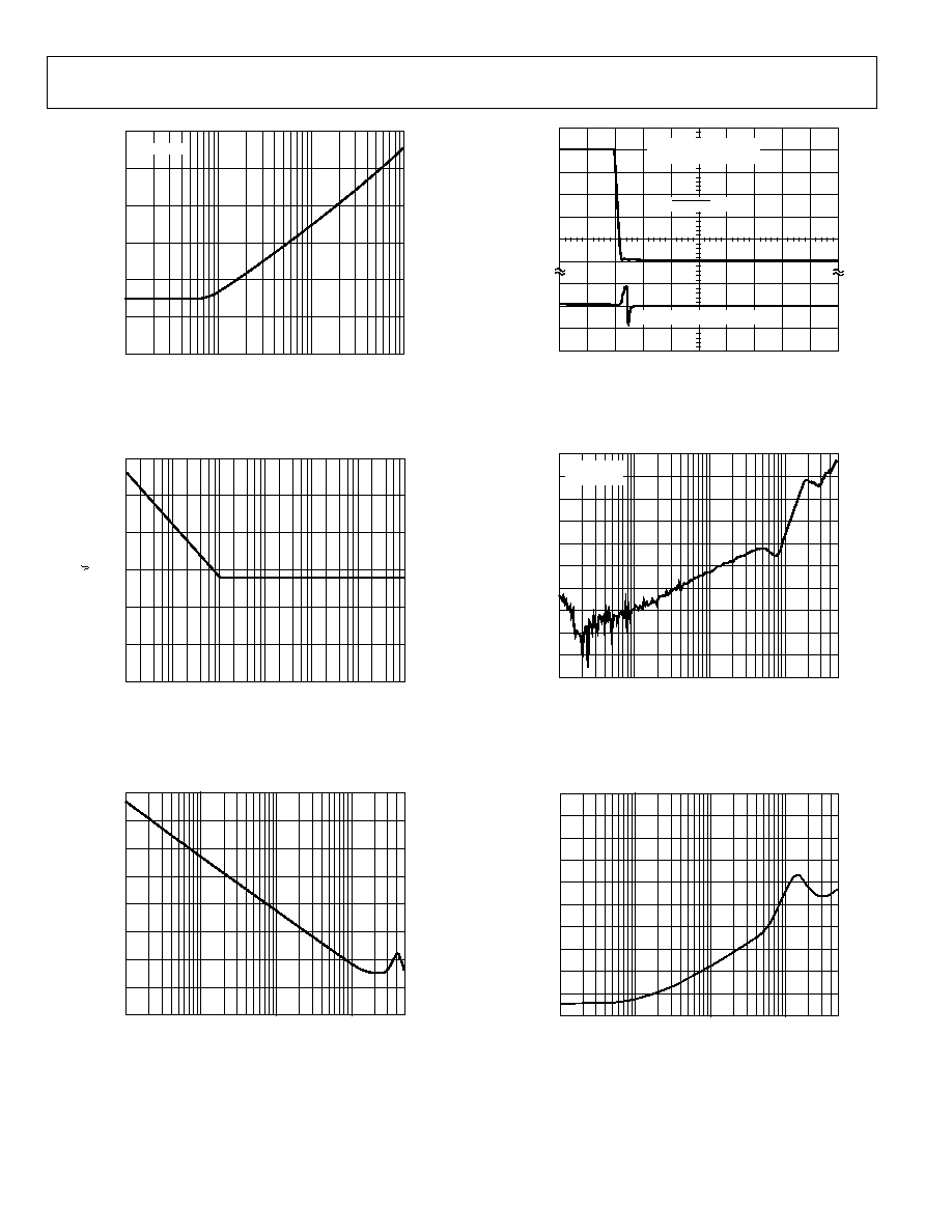
TYPICAL PERFORMANCE CHARACTERISTICS
50
25
0
25
50
0
5
77
4-
0
14
25
m
V
/
D
I
V
25ns/DIV
R
L
= 150
2
1
0
1
3
100k
1M
1G
10M
100M
0.2
0.1
0
0.1
0.2
0.3
2
3
0.3
4
5
GA
IN
(
d
B
)
F
L
AT
NE
S
S
(
d
B)
FREQUENCY (Hz)
FLATNESS
GAIN
2V p-p
200mV p-p
R
L
= 150
05
77
4-
0
11
Figure 13. AD8106 Step Response, 100 mV Step
Figure 10. AD8106 Frequency Response
1.0
0.5
0
0.5
1.0
0
57
74-
015
0.
5
V
/
D
I
V
25ns/DIV
R
L
= 150
30
40
100
0.3
1
200
10
100
50
60
70
80
90
C
R
O
S
S
TA
LK
(
dB
)
FREQUENCY (Hz)
R
L
= 1k
ADJACENT
ALL HOSTILE
05
77
4-
01
2
Figure 11. AD8106 Crosstalk vs. Frequency
Figure 14. AD8106 Step Response, 2 V Step
0
10
20
30
40
50
60
70
80
05
77
4-
0
16
0.
1
%
/
D
I
V
10ns/DIV
2V = STEP
R
L
= 150
100k
1M
100M
10M
100
40
50
60
70
80
90
R
L
= 150
V
OUT
= 2V p-p
3RD HARMONIC
2ND HARMONIC
D
I
S
T
OR
TI
ON
(
d
B
)
FREQUENCY (Hz)
05
77
4-
01
3
Figure 12. AD8106 Distortion vs. Frequency
Figure 15. AD8106 Settling Time
AD8106/AD8107
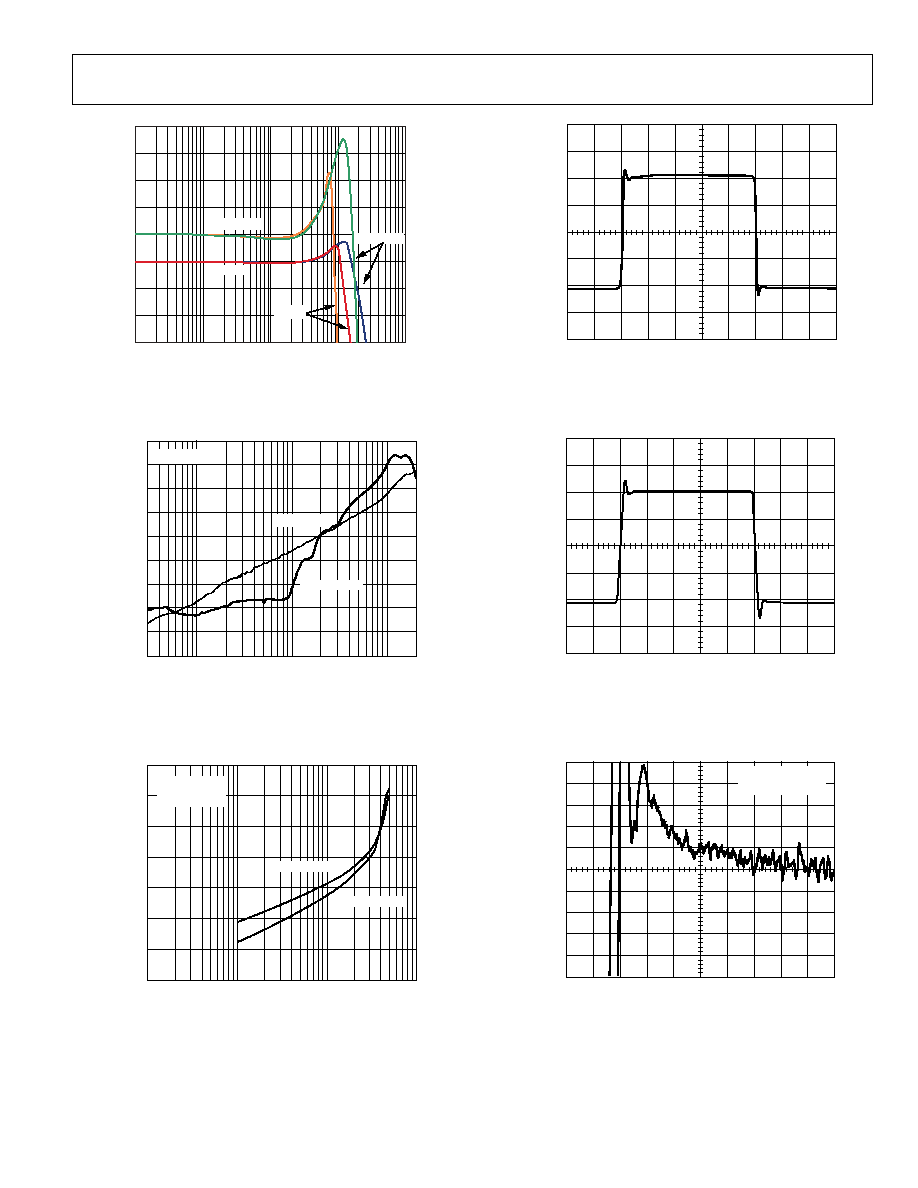
Rev. 0 | Page 11 of 28
1.0
0.5
0
0.5
1.0
25
mV
/
D
I
V
25ns/DIV
05
77
4-
0
20
FREQUENCY (Hz)
2
1
0
1
3
100k
1M
1G
10M
100M
F
L
AT
NE
S
S
(
d
B)
0.4
0.2
0
0.2
0.4
2
3
0.6
GAIN
FLATNESS
0.6
0.8
200mV p-p
0.8
4
5
2V p-p
GA
IN
(
d
B
)
05
774
-
0
17
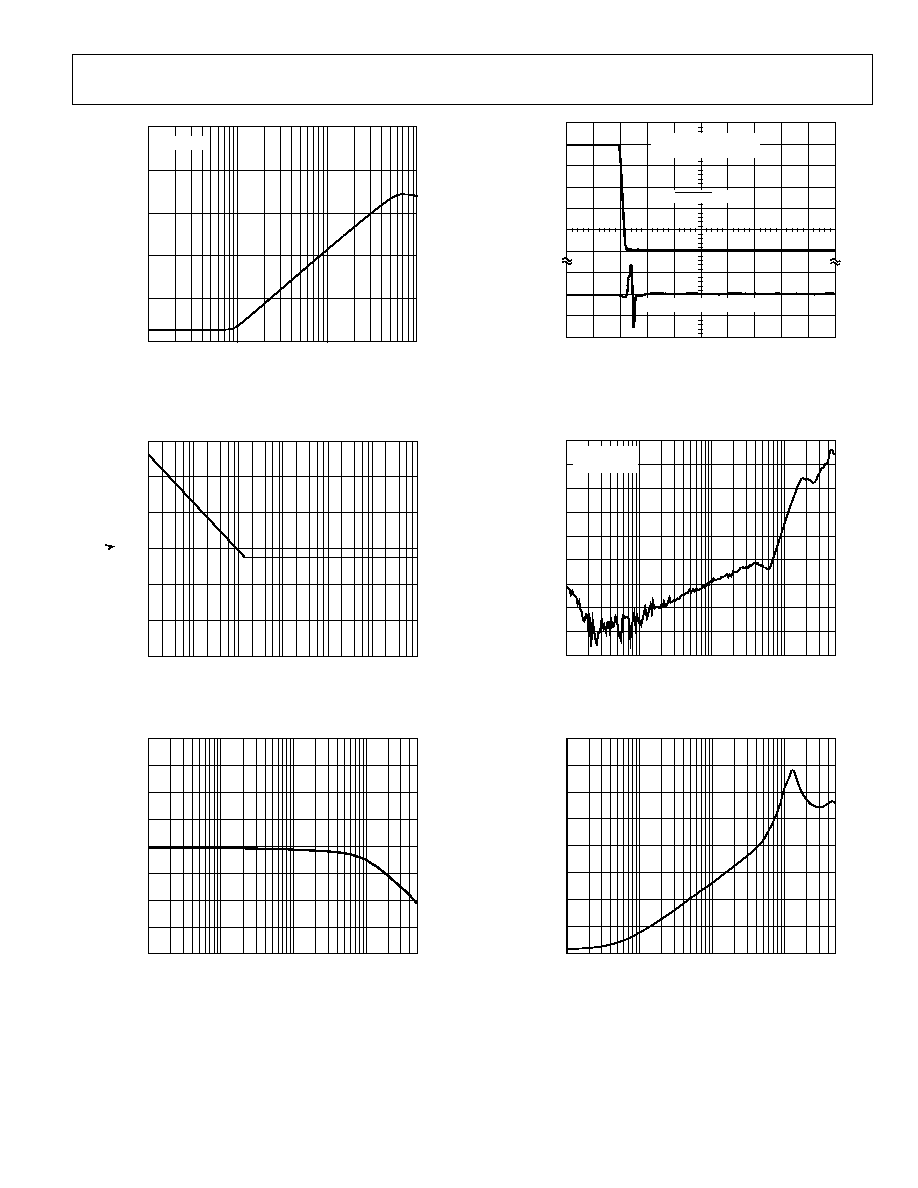
Figure 16. AD8107 Frequency Response
Figure 19. AD8107 Step Response, 100 mV Step
1.0
0.5
0.5
0
1.0
50
0m
V
/
DI
V
25ns/DIV
0
577
4-
0
21
20
30
90
0.3
1
200
10
100
40
50
60
70
80
100
110
R
L
= 1k
ADJACENT
ALL HOSTILE
05
77
4-
0
18
CR
O
S
S
T
A
L
K (
d
B
)
FREQUENCY (MHz)
Figure 20. AD8107 Step Response, 2 V Step
Figure 17. AD8107 Crosstalk vs. Frequency
2V STEP RTO
R
L
= 150
0.
1%/
D
I
V
10ns/DIV
05
77
4-
0
22
0
10
20
30
40
50
60
70
80
30
40
100
50
60
70
80
90
2ND HARMONIC
3RD HARMONIC
100k
1M
10M
100M
D
I
S
T
OR
TION
(
d
B
)
FREQUENCY (Hz)
R
L
= 150
V
OUT
= 2V p-p
05
77
4-
01
9
Figure 21. AD8107 Settling Time
Figure 18. AD8107 Distortion vs. Frequency
AD8106/AD8107
Rev. 0 | Page 12 of 28
UPDATE INPUT
TYPICAL VIDEO OUT (RTO)
5
4
3
2
1
0
10
10
0
SWITCHING BETWEEN
TWO INPUTS
10
mV
/
D
I
V
1V/
D
I
V
0
57
74-
026
50ns/DIV
05
77
4-
02
3
P
O
W
E
R S
UP
P
L
Y
RE
J
E
CT
I
O
N RA
T
I
O
(
d
B)
FREQUENCY (Hz)
30
40
10k
100k
10M
1M
50
60
70
80
90
R
L
= 150
Figure 22. AD8106 PSRR vs. Frequency
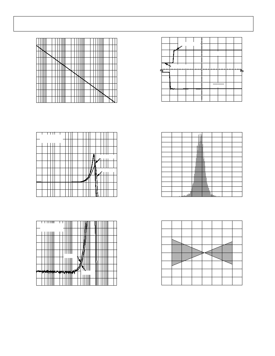
Figure 25. AD8106 Switching Transient (Glitch)
100k
1M
500M
10M
100M
50
60
70
80
90
100
110
120
130
05
77
4-
0
27
O
F
F
I
S
O
L
AT
I
O
N (
d
B)
FREQUENCY (Hz)
V
IN
= 2V p-p
R
L
= 150
100.00
56.30
10
1k
10M
100k
31.60
17.80
10.00
5.630
3.16
100
10k
1M
(nV/
H
z
)
FREQUENCY (Hz)
0
577
4-
0
24
Figure 23. AD8106 Voltage Noise vs. Frequency
Figure 26. AD8106 Off Isolation, Input/Output
10k
1k
100
10
1
0.1
100k
1M
500M
10M
100M
05
77
4-
0
28
OU
TP
U
T
IMP
E
D
A
N
C
E
(
)
FREQUENCY (Hz)
1M
0.1
1
500
10
100k
10k
1k
100
100
0
577
4-
0
25
O
UT
P
UT
I
M
P
E
DANC
E
(
)
FREQUENCY (MHz)
Figure 24. AD8106 Output Impedance, Disabled
Figure 27. AD8106 Output Impedance, Enabled
AD8106/AD8107
Rev. 0 | Page 13 of 28
UPDATE INPUT
TYPICAL VIDEO OUT (RTO)
5
4
3
2
1
0
10
10
0
SWITCHING BETWEEN
TWO INPUTS
10mV
/
DI
V
1
V
/D
IV
05
77
4-
03
2
50ns/DIV
05
77
4-
0
29
P
O
W
E
R
S
U
P
P
L
Y
R
E
JE
CT
I
O
N RAT
I
O
(
d
B RT
I
)
FREQUENCY (Hz)
10k
100k
1M
10M
30
40
50
60
70
80
R
L
= 150
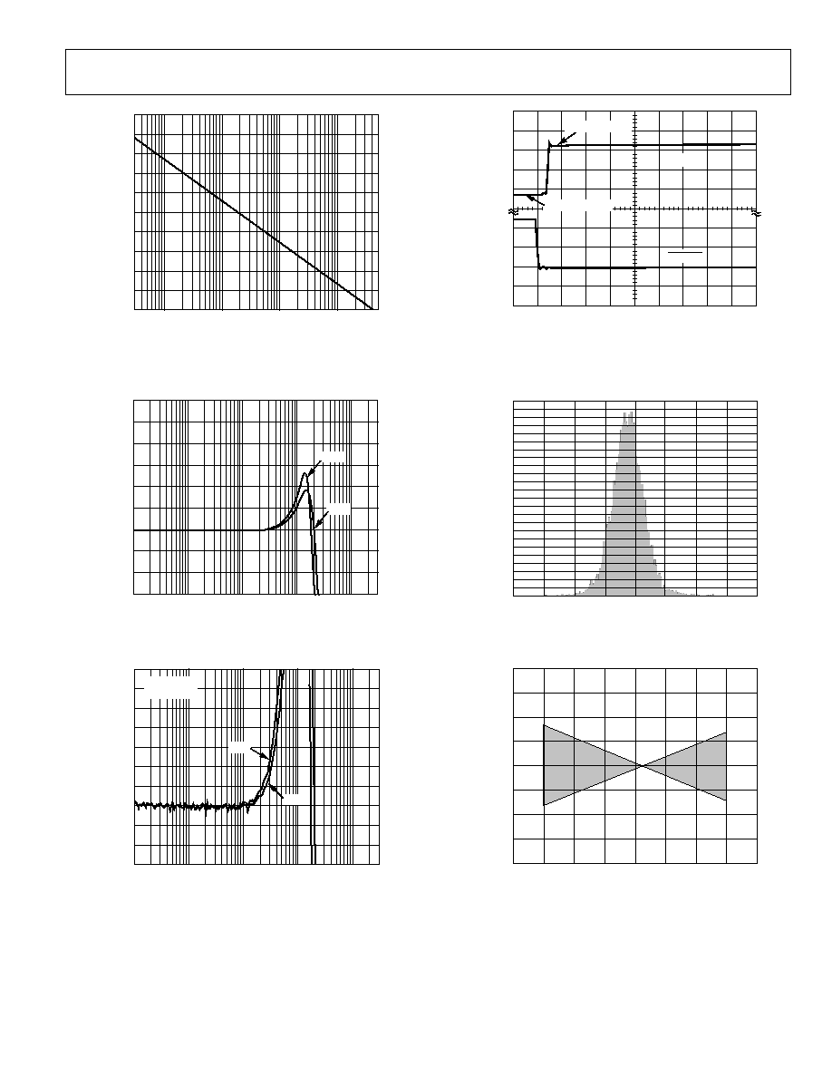
Figure 28. AD8107 PSRR vs. Frequency
Figure 31. AD8107 Switching Transient (Glitch)
100.00
56.30
10
1k
10M
100k
31.60
17.80
10.00
5.63
3.16
100
10k
1M
(n
V/
H
z
)
FREQUENCY (Hz)
05
77
4-
0
30
100k
1M
500M
10M
100M
50
40
60
70
80
90
100
110
120
130
05
77
4-
0
33
O
F
F
I
S
O
L
AT
I
O
N (
d
B)
FREQUENCY (Hz)
`V
OUT
= 2V p-p
R
L
= 150
Figure 32. AD8107 Off Isolation, Input/Output
Figure 29. AD8107 Voltage Noise vs. Frequency
1k
100
10
1
0.1
100k
1M
500M
10M
100M
05
77
4-
0
34
O
U
T
P
UT
I
M
PE
DA
NCE
(
)
FREQUENCY (Hz)
100k
0.1
1
500
10
10k
1k
100
10
100
05
77
4-
03
1
O
UT
P
UT
I
M
P
E
DANC
E
(
)
FREQUENCY (MHz)
Figure 33. AD8107 Output Impedance, Enabled
Figure 30. AD8107 Output Impedance, Disabled
AD8106/AD8107
Rev. 0 | Page 14 of 28
V
OUT
UPDATE
INPUT 1 AT +1V
INPUT 0 AT 1V
1
0
1
5
0
2V
/
D
I
V
1V/
D
I
V
0
57
74-
03
8
50ns/DIV
05
77
4-
0
35
I
N
PUT
I
M
P
E
D
ANCE
(
)
FREQUENCY (Hz)
1M
100k
10k
1k
100
10M
30k
100k
1M
10M
100M
500M
Figure 37. AD8106 Switching Time
Figure 34. AD8106 Input Impedance vs. Frequency
14
12
4
0.1M
1M
10M
100M
1G
10
8
0
6
4
2
2
18pF = 7.7dB
12pF = 4.5dB
3G
V
IN
= 200mV p-p
R
L
= 150
05
77
4-
03
6
GA
IN
(
d
B
)
FREQUENCY (Hz)
260
60
0.02
0.01
0
0.01
240
180
160
120
80
220
200
140
100
40
20
0
0.02
05
77
4-
03
9
F
R
E
Q
UENCY
OFFSET VOLTAGE (V)
Figure 35. AD8106 Frequency Response vs. Capacitive Load
Figure 38. AD8106 Offset Voltage Distribution
2.0
2.0
60
40
100
20
0
20
40
60
80
1.5
0
0.5
1.0
1.5
1.0
0.5
05
77
4-
0
40
V
OS
(m
V)
TEMPERATURE (°C)
05
77
4-
0
37
FLA
T
N
E
S
S
(
d
B
)
FREQUENCY (Hz)
0.7
0.6
0.2
0.1M
1M
10M
100M
1G
0.5
0.4
0
0.3
0.2
0.1
0.1
C
L
= 18pF
C
L
= 12pF
3G
V
IN
= 200mV p-p
R
L
= 150
Figure 39. AD8106 Offset Voltage vs. Temperature (Normalized at 25°C)
Figure 36. AD8106 Flatness vs. Capacitance Load
AD8106/AD8107
Rev. 0 | Page 15 of 28
V
OUT
UPDATE
INPUT 1 AT +1V
INPUT 0 AT 1V
1
0
1
5
0
2V
/
D
I
V
1
V
/D
IV
05
77
4
-
04
4
50nS/DIV
30k
1M
500M
10M
100M
1M
100k
10k
1k
100
100k
10M
05
77
4-
0
41
I
N
PUT
I
M
P
E
DA
NCE
(
)
FREQUENCY (Hz)
Figure 40. AD8107 Input Impedance vs. Frequency
Figure 43. AD8107 Switching Time
12
10
6
8
6
2
4
2
0
4
0.1M
1M
10M
100M
1G
3G
18pF
12pF
05
77
4-
0
42
GA
IN
(
d
B
)
FREQUENCY (Hz)
120
480
360
320
240
160
440
400
280
200
80
40
0
0.02
0.02
0.01
0
0.01
05
77
4-
0
45
F
R
EQ
UE
NCY
OFFSET VOLTAGE (V)
Figure 44. AD8107 Offset Voltage Distribution (RTI)
Figure 41. AD8107 Frequency Response vs. Capacitive Load
0.7
0.6
0.1
0.5
0.4
0
0.3
0.2
0.1
0.2
0.3
0.1M
1M
10M
100M
1G
3G
12pF
18pF
V
IN
= 100mV
R
L
= 150
05
77
4-
04
3
GA
IN
(
d
B
)
FREQUENCY (Hz)
2.0
2.0
60
40
100
20
0
20
40
60
80
1.5
0
0.5
1.0
1.5
1.0
0.5
05
77
4-
0
46
V
OS
(m
V)
TEMPERATURE (°C)
Figure 45. AD8107 Offset Voltage Drift vs. Temperature (Normalized at 25°C)
Figure 42. AD8107 Flatness vs. Capacitive Load

AD8106/AD8107
Rev. 0 | Page 16 of 28
THEORY OF OPERATION
The AD8106 (G = 1) and AD8107 (G = 2) share a common core
architecture consisting of an array of 80 transconductance (gm)
input stages that are organized as five 16:1 multiplexers with a
common, 16-line analog input bus. Each multiplexer is
essentially a folded-cascode high speed voltage, feedback
amplifier with 16 input stages. The input stages are NPN
differential pairs whose differential current outputs are
combined at the output stage, which contains the high
impedance node, compensation, and a complementary emitter
follower output buffer. In the AD8106, the output of each
multiplexer is fed directly back to the inverting inputs of its
16 gm stages. In the AD8107, the feedback network is a voltage
divider consisting of two equal-value resistors.
This switched-gm architecture results in a low power crosspoint
switch that is able to directly drive a back-terminated video load
(150 ) with low distortion (differential gain and differential
phase errors are better than 0.02% and 0.02°, respectively). This
design also achieves high input resistance and low input
capacitance without the signal degradation and power
dissipation of additional input buffers. However, the small input
bias current at any input increases almost linearly with the
number of outputs programmed to that input.
The output disable feature of these crosspoints allows larger
switch matrices to be built simply by busing together the
outputs of multiple 16 × 5 ICs. However, while the disabled
output impedance of the AD8106 is very high (10 M), the
AD8107 output impedance is limited by the resistive feedback
network, which has a nominal total resistance of 1 k and
appears in parallel with the disabled output. If the outputs of
multiple AD8107s are connected through separate back
termination resistors, the loading lowers the effective back
termination impedance of the overall matrix because of these
finite output impedances. This problem is eliminated if the
outputs of multiple AD8107s are connected directly and share a
single back-termination resistor for each output of the overall
matrix. This configuration increases the capacitive loading of
the disabled AD8107 on the output of the enabled AD8107.
POWER-ON RESET
When powering up the AD8106/AD8107, it is usually necessary
to have the outputs be in the disabled state. The RESET pin,
when taken low, causes all outputs to be in the disabled state.
The RESET pin has a 20 k pull-up resistor to DVDD that can
be used to create a simple power-up reset circuit. A capacitor
from RESET to ground holds RESET low for some time while
the rest of the device stabilizes. The low condition causes all the
outputs to disable. The capacitor then charges through the pull-
up resistor to the high state, allowing full programming
capability of the device.
INITIALIZATION
The AD8106/AD8107 should be initialized after power up to
control the supply and bias currents, and to make sure that no
unexpected program states are encountered. Initialization is
performed by writing a data word of 00000 into all address
locations 00 to 07 (000 to 111 binary).
GAIN SELECTION
The 16 × 5 crosspoints come in two versions depending on the
desired gain of the analog circuit paths. The AD8106 device is
unity gain and can be used for analog logic switching and other
applications where unity gain is desired. The AD8106 can also
be used for the input and interior sections of larger crosspoint
arrays where termination of output signals is not usually used.
The AD8106 outputs have very high impedance when their
outputs are disabled.
For devices that drive a terminated cable with its outputs, the
AD8107 can be used. This device has a built-in gain of two that
eliminates the need for a gain-of-two buffer to drive a video
line. Because of the presence of the feedback network in these
devices, the disabled output impedance is about 1 k.
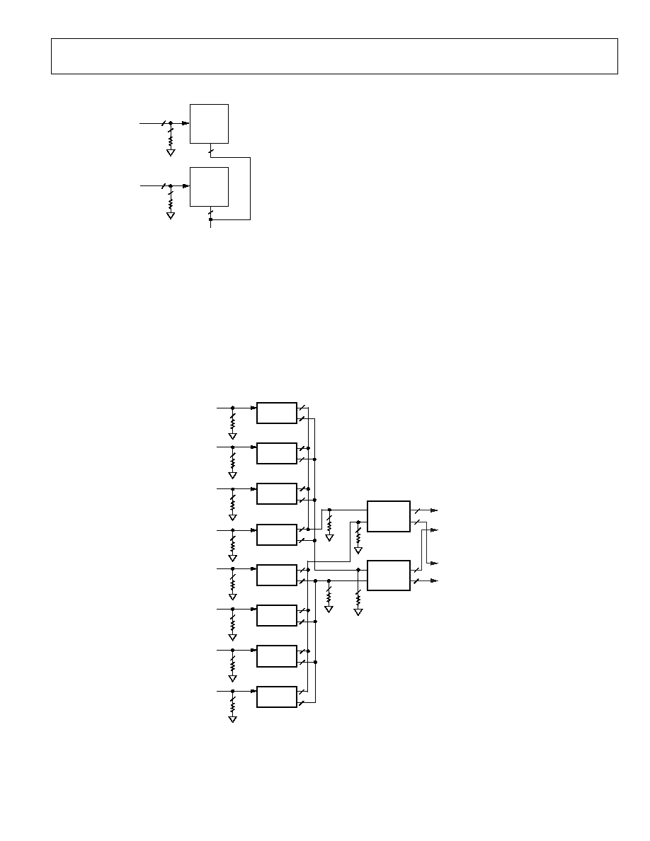
CREATING LARGER CROSSPOINT ARRAYS
The AD8106/AD8107 are high density building blocks that
create crosspoint arrays for dimensions larger than 16 × 5.
Various features such as output disable, chip enable, and gain-
of-one and gain-of-two options are useful for creating larger
arrays. For very large arrays, they can be used with the
AD8114
/
AD8115
, 16 × 16 video crosspoint devices, or the
AD8110
/
AD8111
, 16 x 8 video crosspoint devices. When required
for customizing a crosspoint array size, the parts can also be
used with the
AD8108
and
AD8109
, a pair (unity gain and
gain-of-two) of 8 × 8 video crosspoint switches.
The first consideration in constructing a larger crosspoint is to
determine the minimum number of required devices. The 16 × 5
architecture of the AD8106/AD8107 contains 80 points. For a
nonblocking crosspoint, the number of points required is the
product of the number of inputs multiplied by the number of
outputs. Nonblocking requires that the programming of a given
input to one or more outputs does not restrict the availability of
that input to be a source for any other output.
Some nonblocking crosspoint architectures require more than this
minimum as calculated above. In addition, there are blocking
architectures that can be constructed with fewer devices than this
minimum. These systems have connectivity available on a statistical
basis that is determined when designing the overall system.
The basic concept in constructing larger crosspoint arrays is to
connect inputs in parallel in a horizontal direction and to wire-OR
the outputs together in a vertical direction.
AD8106/AD8107
Rev. 0 | Page 17 of 28
Figure 46 illustrates this concept for a 32 × 5 crosspoint array.
AD8106
OR
AD8107
16
16
R
TERM
R
TERM
IN 0015
AD8106
OR
AD8107
16
16
IN 1631
5
5
0
57
74
-
04
7
Figure 46. A 32 × 5 Crosspoint Array Using Two AD8106s or Two AD8107s
The inputs are uniquely assigned to each of the 32 inputs of the
two devices and terminated appropriately. The outputs are wire-
OR'ed together in pairs. The output from only one of a wire-OR'ed
pair should be enabled at any given time. The device program-
ming software must be properly written to cause this to happen.
At some point, the number of outputs that are wire-OR'ed becomes
too great to maintain system performance. This varies according
to which system specifications are most important. It also
depends on whether the matrix consists of AD8106s or AD8107s.
The output disabled impedance of the AD8106 is much
higher than that of the AD8107. As a result, its disabled
parasitics have a smaller effect on the one output that is
enabled. For example, a 128 × 5 crosspoint can be created
with eight AD8106s/AD8107s. This design has 128 separate
inputs and the corresponding outputs of each device wire-
OR'ed together in groups of eight.
Using additional crosspoint devices in the design can lower the
number of outputs that must be wire-OR'ed together. Figure 47
shows a block diagram of a system using eight AD8106s and
two AD8107s to create a nonblocking, gain-of-two, 128 × 5
crosspoint that restricts the wire-OR'ing at the output to only
four outputs.
Additionally, by using the lower four outputs from each of the
two Rank 2 AD8107s, a blocking 128 × 10 crosspoint array can
be realized. There are, however, some drawbacks to this technique.
The offset voltages of the various cascaded devices accumulate
and the bandwidth limitations of the devices compound. The
extra devices also consume more current and take up more
board space. Once again, the overall system design specifica-
tions determine which tradeoffs should be made.
5
5
5
5
RANK 2
16:8 NONBLOCKING
(16:16 BLOCKING)
RANK 1
(8 × AD8106)
128:16
5
5
5
5
AD8107
AD8107
AD8106
AD8106
AD8106
AD8106
AD8106
AD8106
AD8106
AD8106
OUT 0004
NONBLOCKING
ADDITIONAL
5 OUTPUTS
(SUBJECT TO
BLOCKING)
1k
1k
1k
1k
05
77
4-
0
48
5
5
5
5
5
5
5
5
5
5
5
5
5
5
5
5
16
IN 0015
R
TERM
16
IN 1631
R
TERM
16
IN 3247
R
TERM
16
IN 4863
R
TERM
16
IN 6479
R
TERM
16
IN 8095
R
TERM
16
IN 96111
R
TERM
16
IN 112127
R
TERM
Figure 47. A Gain-of-Two 128 × 5 Nonblocking Crosspoint Array (128 × 10 Blocking)

AD8106/AD8107
Rev. 0 | Page 18 of 28
In addition, crosstalk can occur among the inputs to a
crosspoint as well as among the outputs. It can also occur
from input to output. Refer to the
CROSSTALK
Many systems, such as broadcast video, handle numerous
analog signal channels that have strict requirements for keeping
the various signals from influencing others in the system.
Crosstalk is the term used to describe the undesired coupling
between signals of other nearby channels to a given channel.
Input and Output Crosstalk
section for techniques to diagnose which part of a system is
contributing to crosstalk.
Measuring Crosstalk
Crosstalk is measured by applying a signal to one or more
channels and measuring the relative strength of that signal on a
desired selected channel. The measurement is usually expressed
as dB down from the magnitude of the test signal. The crosstalk
is expressed by
When many signals are in close proximity in a system, as is
undoubtedly the case in a system that uses the AD8106/
AD8107, the crosstalk issues can be quite complex. A good
understanding of the nature of crosstalk and its associated
terms is required to specify a system that uses one or more
AD8106s/AD8107s.
( )
( )
(
)
s
Atest
s
Asel
XT
/
log
20
10
=
(1)
Types of Crosstalk
where:
Crosstalk can be propagated by means of one of three methods.
These fall into the categories of electric field, magnetic field, and
sharing of common impedances. This section explains these effects.
s = jw is the Laplace transform variable.
Asel(s) is the amplitude of the crosstalk-induced signal in the
selected channel.
Atest(s) is the amplitude of the test signal.
Every conductor can be both a radiator of electric fields and a
receiver of electric fields. The electric field crosstalk mechanism
occurs when the electric field created by the transmitter
propagates across a stray capacitance (free space, for example),
couples with the receiver, and induces a voltage. This voltage is
an unwanted crosstalk signal in any channel that receives it.
It can be seen that crosstalk is a function of frequency, but not a
function of the test signal's magnitude (to first order). The crosstalk
signal also has a phase relative to its associated test signal.
A network analyzer is most commonly used to measure
crosstalk over a frequency range of interest. It can provide both
magnitude and phase information about the crosstalk signal.
Currents flowing into conductors create magnetic fields that
circulate around the currents. These magnetic fields then
generate voltages in any other conductors whose paths they
link. The undesired induced voltages in these channels are
crosstalk signals. The channels that crosstalk have a mutual
inductance that couples signals from one channel to another.
As a crosspoint system or device grows, the number of theoretical
crosstalk combinations and permutations can become extremely
large. For example, in the case of the 16 x 5 matrix of the
AD8106/AD8107, examine the number of crosstalk terms that
can be considered for a single channel, such as the IN00 input.
IN00 is programmed to connect to one of the AD8106/AD8107
outputs where the measurement can be made.
The power supplies, grounds, and other signal return paths of a
multichannel system are generally shared by the various
channels. When a current from one channel flows into one of
these paths, a voltage develops across the impedance and
becomes an input crosstalk signal for other channels that share
the common impedance.
First, measure the crosstalk terms associated with driving a test
signal into each of the other 15 inputs one at a time. Then measure
the crosstalk terms associated with driving a parallel test signal
into all 15 other inputs taken two at a time in all possible
combinations; and then three at a time, and so on, until finally,
there is only one way to drive a test signal into all 15 other inputs.
All these sources of crosstalk are vector quantities, so the magni-
tudes cannot simply be added together to obtain the total crosstalk.
In fact, there are conditions when driving additional circuits in
parallel in a given configuration can actually reduce the crosstalk.
Each of these cases is legitimately different from the others and
could yield a unique value depending on the resolution of the
measurement system. However, it is impractical to measure all
of these terms and then to specify them. In addition, this
describes the crosstalk matrix for only one input channel. A
similar crosstalk matrix can be proposed for every other input.
If the possible combinations and permutations for connecting
inputs to the other outputs (not used for measurement) are
taken into consideration, the numbers grow rather quickly to
astronomical proportions. If a larger crosspoint array of
multiple AD8106/AD8107s is constructed, the numbers grow
larger still.
Areas of Crosstalk
A practical AD8106/AD8107 circuit is required to be mounted
to some sort of circuit board to connect to power supplies and
measurement equipment. Great care has been taken to create a
characterization board (also available as an evaluation board) that
adds minimum crosstalk to the intrinsic device. This, however,
raises the issue that a system's crosstalk is a combination of the
device's intrinsic crosstalk and the circuit board to which they
are mounted. It is important to try to separate these two areas of
crosstalk when attempting to minimize its effect.

AD8106/AD8107
Rev. 0 | Page 19 of 28
Obviously, some subset of all these cases must be selected to be
used as a guide for a practical measure of crosstalk. One
common method is to measure all hostile crosstalk, which
means that the crosstalk to the selected channel is measured
while all other system channels are driven in parallel. In general,
this yields the worst crosstalk number, but this is not always the
case due to the vector nature of the crosstalk signal.
From a circuit standpoint, the input crosstalk mechanism looks
like a capacitor coupling to a resistive load. For low frequencies,
the magnitude of the crosstalk is given by
(
)
[
]
s
C
R
XT
M
S
×
=
10
log
20
(2)
where:
R
S
is the source resistance.
C
Other useful crosstalk measurements are those created by one
of the nearest neighbors or by two of the nearest neighbors on
either side. These crosstalk measurements are generally higher
than those of more distant channels, so they can serve as a
worst-case measure for any other one-channel or two-channel
crosstalk measurements.
M
is the mutual capacitance between the test signal circuit and
the selected circuit.
s is the Laplace transform variable.
Equation 2 shows that this crosstalk mechanism has a high-pass
nature; it can also be minimized by reducing the coupling
capacitance of the input circuits and lowering the output
impedance of the drivers. If the input is driven from a 75
terminated cable, the input crosstalk can be reduced by
buffering this signal with a low output impedance buffer.
Input and Output Crosstalk
The flexible programming capability of the AD8106/AD8107
can be used to diagnose whether crosstalk is occurring more on
the input side or the output side. For example, a given input
channel, such as IN07 in the middle, can be programmed to
drive OUT01. The input to IN07 is terminated to ground (via
50 or 75 ) and no signal is applied.
On the output side, the crosstalk can be reduced by driving a
lighter load. Although the AD8106/AD8107 are specified with
excellent differential gain and phase when driving a standard
150 video load, the crosstalk is higher than the minimum
obtainable because of the high output currents. These currents
induce crosstalk via the mutual inductance of the output pins
and bond wires of the AD8106/AD8107.
All the other inputs are driven in parallel with the same test
signal (practically provided by a distribution amplifier) with all
other outputs disabled, except OUT01. Because grounded IN07
is programmed to drive OUT01, no signal should be present. If
any signal is present, it can be attributed to the other 15 hostile
input signals because no other outputs are driven; that is, they
are all disabled. Thus, this method measures the all-hostile input
contribution to crosstalk into IN07. This method can also be used
for other input channels and combinations of hostile inputs.
From a circuit standpoint, this output crosstalk mechanism
looks like a transformer with a mutual inductance between the
windings that drive a load resistor. For low frequencies, the
magnitude of the crosstalk is given by
(
)
L
R
s
Mxy
XT
/
log
20
10
×
=
(3)
For output crosstalk measurement, a single input channel
(IN00, for example) is driven and all outputs other than a given
output are programmed to connect to IN00. OUT01 is
programmed to connect to IN15, which is far away from IN00,
and is terminated to ground. As a result, OUT01 should not
have a signal present because it is listening for a quiet input.
Any signal measured at the OUT01 can be attributed to the
output crosstalk of the other seven hostile outputs. Again, this
method can be modified to measure other channels and other
crosspoint matrix combinations.
where:
Mxy is the mutual inductance of output x to output y.
R is the load resistance on the measured output.
L
This crosstalk mechanism can be minimized by keeping the
mutual inductance low and increasing R
L
. The mutual
inductance can be kept low by increasing the spacing of the
conductors and minimizing their parallel length.
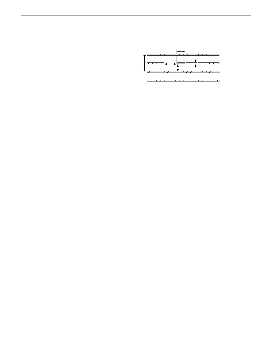
PCB LAYOUT
Effect of Impedances on Crosstalk
Extreme care must be exercised to minimize additional
crosstalk generated by the system circuit board(s). The areas
that must be carefully detailed are grounding, shielding, signal
routing, and supply bypassing.
The input side crosstalk can be influenced by the output
impedance of the sources that drive the inputs. The lower the
impedance of the drive source, the lower the magnitude of the
crosstalk. The dominant crosstalk mechanism on the input side
is capacitive coupling. The high impedance inputs do not have
significant current flow to create magnetically induced crosstalk.
However, significant current can flow through the input
termination resistors and the loops that drive them. Thus,
the PC board on the input side can contribute to magnetically
coupled crosstalk.
The packaging of the AD8106/AD8107 is designed to help keep
the crosstalk to a minimum. Each input is separated from other
inputs by an analog ground pin. All of these AGNDs should be
connected directly to the ground plane of the circuit board.
These ground pins provide shielding, low impedance return
paths, and physical separation for the inputs. All of these help to
reduce crosstalk.

AD8106/AD8107
Rev. 0 | Page 20 of 28
Each output is separated from its two neighboring outputs by an
analog ground pin and an analog supply pin of one polarity or
the other. Each of these analog supply pins provides power to
the output stages for only the two nearest outputs. These supply
pins and analog grounds provide shielding, physical separation,
and a low impedance supply for the outputs. Individual
bypassing of these supply pins with a 0.01 F chip capacitor
directly to the ground plane minimizes high frequency output
crosstalk via the mechanism of sharing common impedances.
Each output also has an on-chip compensation capacitor that is
individually tied to the nearby analog ground pins AGND00
through AGND03. This technique reduces crosstalk by preventing
the currents that flow in these paths from sharing a common
impedance on the IC and in the package pins. These AGNDxx
signals should all be connected directly to the ground plane.
The input and output signals have minimum crosstalk if they
are located between ground planes on layers above and below,
and separated by ground in between. Vias should be located as
close to the IC as possible to carry the inputs and outputs to the
inner layer. The only place the input and output signals surface
is at the input termination resistors and the output series back
termination resistors. These signals should also be separated, to
the largest extent possible, as soon as they emerge from the IC
package.
AD8106/AD8107
Rev. 0 | Page 21 of 28
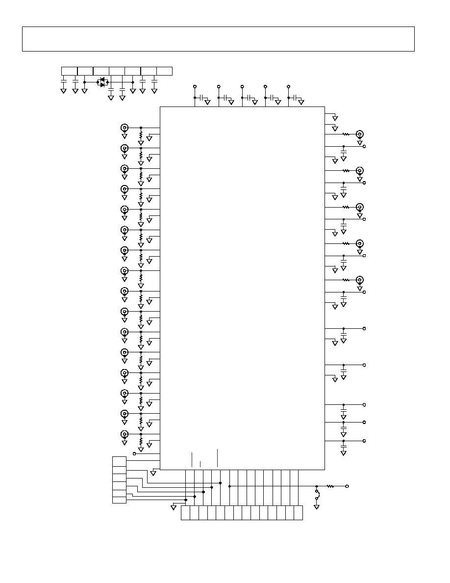
EVALUATION BOARD
w = 0.008"
(0.2mm)
a = 0.008"
(0.2mm)
b = 0.024"
(0.6mm)
h = 0.011325"
(0.288mm)
t = 0.00135" (0.0343mm)
COMPONENT LAYER
SIGNAL ROUTING LAYER
POWER PLANE LAYER
BOTTOM LAYER
05
774-
049
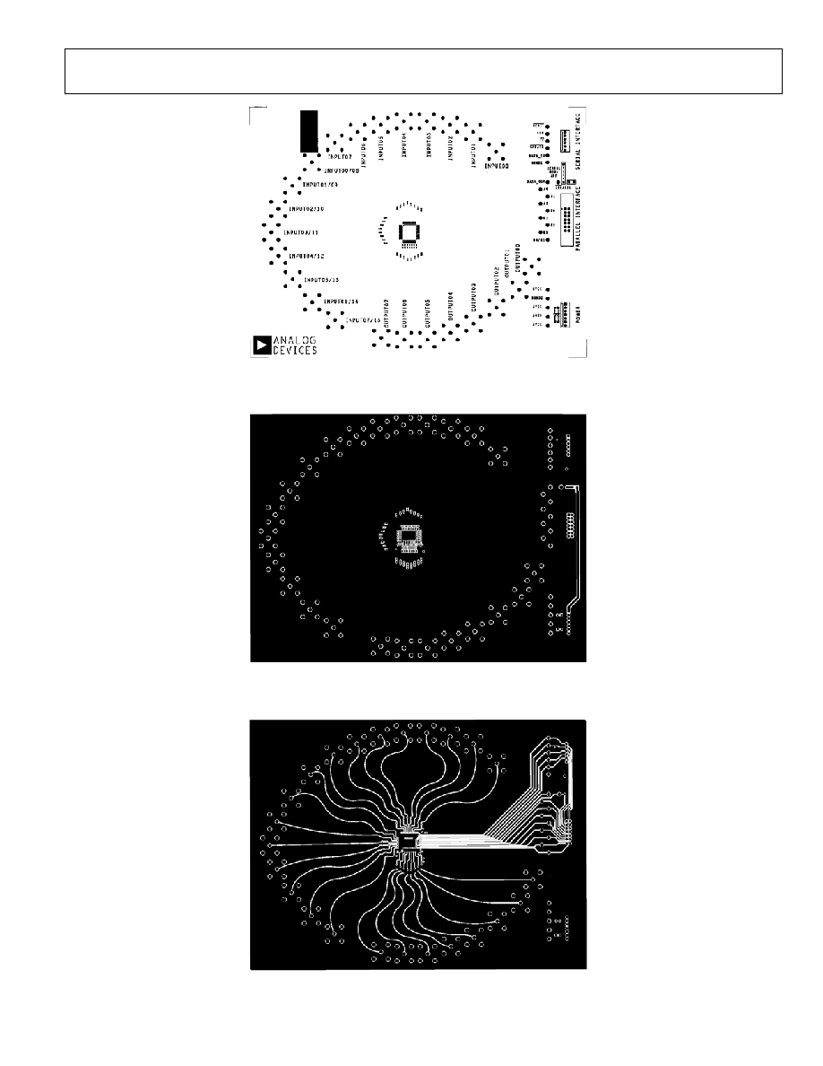
A 4-layer evaluation board is available for the AD8106/
AD8107. The same board and external components are used for
each device. The only difference is the device itself, which offers
a selection of a gain of unity or a gain of two through the analog
channels. This board has been carefully laid out and tested to
demonstrate the specified high speed performance of the
device. Figure 49 shows the schematic of the evaluation board.
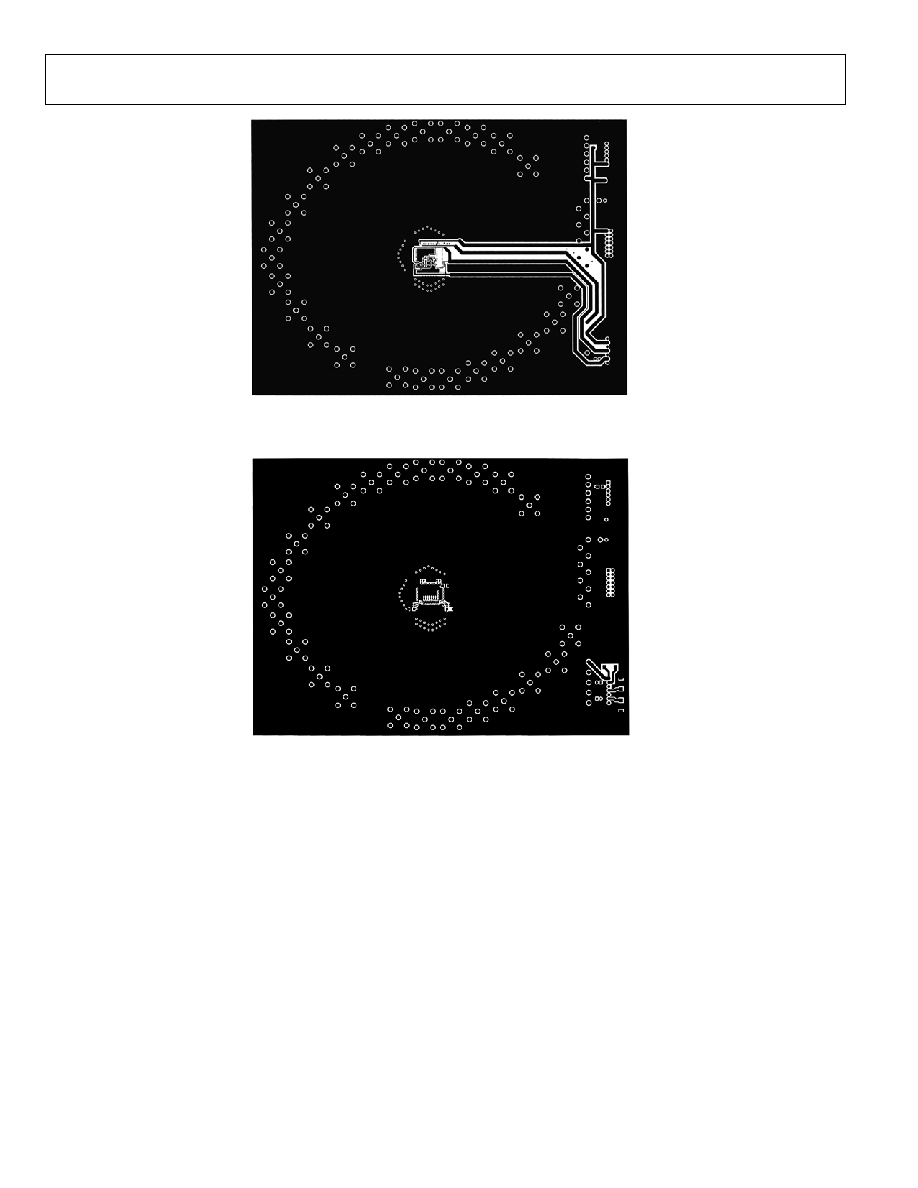
Figure 50 shows the component side silkscreen. The layout of
the board's four layers are given in:
Figure 48. Cross Section of Input and Output Traces
The board has 24 BNC-type connectors: 16 inputs and 8 outputs.
The connectors are arranged in a crescent around the device.
As shown in
·
Component Layer (see Figure 51)
Figure 53, this results in all 16 input signal traces
and all 8 signal output traces having the same length. This is
useful in tests such as all-hostile crosstalk where the phase
relationship and delay between signals needs to be maintained
from input to output.
·
Signal Routing Layer (see Figure 52)
·
Power Layer (see Figure 53)
·
Bottom Layer (see Figure 54)
The evaluation board package includes the following:
The three power supply pins, AVCC, DVCC, and AVEE, should
be connected to good quality, low noise, ±5 V supplies. While
the same ±5 V power supplies are used for analog and digital,
separate cables should be run for the power supply to the
evaluation board's analog and digital power supply pins.
·
Fully populated board with BNC-type connectors.
·
Windows®-based software for controlling the board from a
PC via the printer port.
As a general rule, each power supply pin (or group of adjacent
power supply pins) should be locally decoupled with a 0.01 F
capacitor. If there is a space constraint, decouple analog power
supply pins before digital power supply pins. A 0.1 F capacitor
located reasonably close to the pins can be used to decouple a
number of power supply pins. Finally, a 10 F capacitor should
be used to decouple power supplies as they come on to the board.
·
Custom cable to connect evaluation board to PC.
·
Disk containing Gerber files of board layout.
Optimized for video applications, all signal inputs and outputs
are terminated with 75 resistors. Stripline techniques are used
to achieve a characteristic impedance on the signal input and
output lines, also of 75 . Figure 48 shows a cross section of one
of the input or output tracks along with the arrangement of the
PCB layers. Note that unused regions of the four layers are filled
up with ground planes. As a result, the input and output traces,
in addition to having controlled impedances, are well shielded.
AD8106/AD8107
Rev. 0 | Page 22 of 28
75
AVEE
41
40
39
65
64
INPUT 00
IN00
AGND
DG
ND
CE
R
E
SE
R
V
ED
UP
D
A
T
E
CL
K
A0
A1
A2
D0
D1
D2
D3
D4
62 61 60 58 56 55 54 53 52 51 50 49 48 47
SERIAL MODE
JUMP
R25
20k
DVCC
42
AVCC
38
37
36
AVEE
35
34
33
AVCC
32
31
30
AVEE
29
28
27
AVCC
26
25
24
AVEE
23
22
21
20
AGND
OUT00
AVEE
AGND
OUT01
AVCC
AGND
OUT02
AVEE
AGND
OUT03
AVCC
AGND
OUT04
AVEE
AGND
NC
AVCC
AGND
NC
AVEE
AGND
NC
AVCC
19
AVCC
AVCC
18
AVCC
AVEE
17
AVEE
45
AVEE
AVEE
44
AVCC
AVCC
43
AVCC
AVCC
AD8106/AD8107
DVCC DGND
NC
AVEE AGND AVCC
NC
P1-1
CR1
CR2
+
+
+
P1-2
P1-3
P1-4
P1-5
P1-6
P1-7
0.1µF 10µF
0.1µF 10µF
0.1µF 10µF
P2
-
5
P2
-
4
P2
-
3
P2
-
3
P2
-
1
P2
-
6
P2
-
5
P2
-
4
P2
-
3
P2
-
2
P2
-
1
P2
-
6
P2
-
5
P2
-
4
63
0.01µF
79
DVCC
DVCC
DVCC
DVCC
46
AGND
0.01µF
0.01µF
0.01µF
0.01µF
0.01µF
0.01µF
0.01µF
0.01µF
0.01µF
0.01µF
0.01µF
0.01µF
0.01µF
75
75
75
75
75
67
66
INPUT 01
IN01
AGND
75
69
68
INPUT 02
IN02
AGND
75
71
70
INPUT 03
IN03
AGND
75
73
72
INPUT 04
IN04
AGND
75
75
74
INPUT 05
IN05
AGND
75
77
76
INPUT 06
IN06
AGND
75
78
INPUT 07
IN07
75
2
1
INPUT 08
IN08
AGND
75
4
3
INPUT 09
IN09
AGND
75
6
5
INPUT 10
IN10
AGND
75
8
7
INPUT 11
IN11
AGND
75
10
9
INPUT 12
IN12
AGND
75
12
11
INPUT 14
IN13
AGND
75
14
13
INPUT 14
IN14
AGND
75
16
15
INPUT 15
IN15
AGND
75
RE
S
E
T
05
77
4-
0
50
59
RESERVED
P2-5
P2-4
P2-2
P2-3
P2-1
P2-6
57
RESERVED
80 DGND
Figure 49. Evaluation Board Schematic
AD8106/AD8107
Rev. 0 | Page 23 of 28
0
57
74
-
05
1
AD8106
AD8107
Figure 50. Component Side Silkscreen
05
77
4-
0
52
Figure 51. Board Layout (Component Side)
05
77
4-
0
53
Figure 52. Board Layout (Signal Routing Layer)
AD8106/AD8107
Rev. 0 | Page 24 of 28
0
577
4-
05
4
Figure 53. Board Layout (Power Plane Layer)
05
774
-
05
5
Figure 54. Board Layout (Bottom Layer)
AD8106/AD8107
Rev. 0 | Page 25 of 28
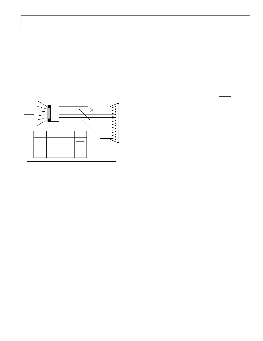
CONTROLLING THE EVALUATION BOARD
FROM A PC
When launching the crosspoint control software, users are
asked to select their desired printer port. Most modern PCs
have only one printer port, usually called LPT1. However, some
laptop computers use the PRN port.
The evaluation board includes Windows-based control software
and a custom cable that connects the board's digital interface to
the printer port of a PC. The wiring of this cable is shown in
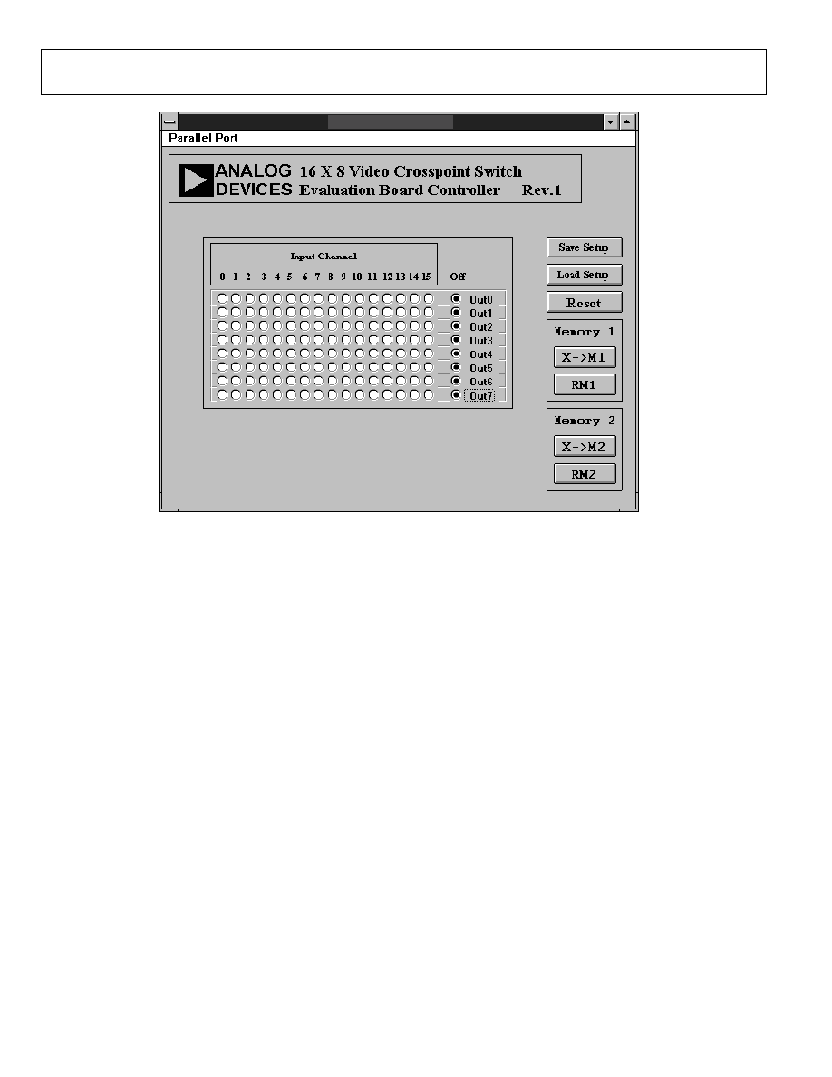
Figure 56 shows the main screen of the control software in its
initial reset state (all outputs off). Using the mouse, any input
can be connected with one or more outputs by simply clicking
on the appropriate radio buttons in the 16 × 8 on-screen array.
Each time a button is clicked on, the software automatically sends
and latches the required 40-bit data stream to the evaluation board.
An output can be turned off by clicking the appropriate button
in the off column. To turn all outputs on, click
Figure 55. The software requires Windows 3.1 or later to operate.
Before the start of the installation, terminate any other Windows
applications that are running. To install the software, insert
the disk labeled Disk #1 of 2 in the PC and run the setup.exe file.
Additional installation instructions are given on-screen.
CLK
DATA IN
RESET
UPDATE
CE
DGND
MOLEX 0.100" CENTER
CRIMP TERMINAL HOUSING
1
6
D-SUB 25 PIN (MALE)
14 1
25
13
EVALUATION BOARD
PC
2
3
4
5
6
25
3
1
4
5
2
6
SIGNAL
DATA IN
CE
RESET
UPDATE
CLK
DGND
MOLEX
TERMINAL HOUSING
D-SUB-25
05
77
4-
05
6
RESET.
The software offers volatile and nonvolatile configuration
storage. For volatile storage, up to two configurations can be
stored and recalled using the Memory 1 Buffer and Memory 2
Buffer. These function in an identical fashion to the memory on
a pocket calculator. For nonvolatile storage of a configuration,
the Save Setup and Load Setup functions can be used. This
stores the configuration as a data file on disk.
DATA-LINE OVERSHOOT ON PRINTER PORTS
The data lines on some printer ports have excessive overshoot.
Overshoot on the pin that is used as the serial clock (Pin 6 on
the D-Sub-25 connector) can cause communication problems.
This overshoot can be eliminated by connecting a capacitor
from the CLK line on the evaluation board to ground. A pad
has been provided on the solder side of the evaluation board to
allow this capacitor to be soldered into place. Depending upon
the overshoot from the printer port, this capacitor may need to
be as large as 0.01 F.
Figure 55. Evaluation Board PC Connection Cable
AD8106/AD8107
Rev. 0 | Page 26 of 28
0
57
74
-
05
7
AD8106/AD8107
Figure 56. Evaluation Board Control Panel
AD8106/AD8107
Rev. 0 | Page 27 of 28
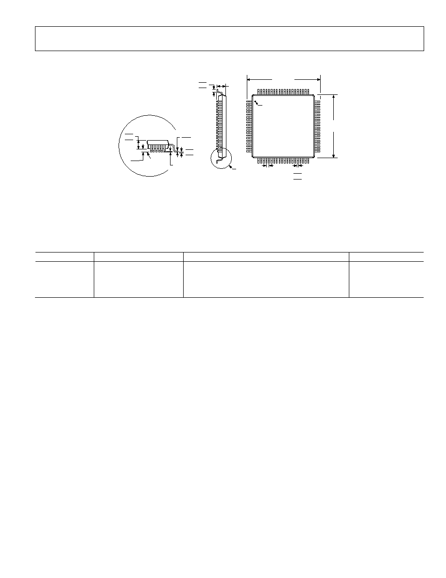
OUTLINE DIMENSIONS
COMPLIANT TO JEDEC STANDARDS MS-026-BDD
0.15
0.05
1.45
1.40
1.35
0.20
0.09
0.08 MAX
COPLANARITY
VIEW A
ROTATED 90° CCW
SEATING
PLANE
7°
3.5°
0°
TOP VIEW
(PINS DOWN)
1
21
41
40
60
61
80
20
12.00
BSC SQ
0.50
BSC
LEAD PITCH
0.27
0.22
0.17
14.00
BSC SQ
1.60
MAX
0.75
0.60
0.45
VIEW A
PIN 1
Figure 57. 80-Lead Low Profile Quad Flat Package [LQFP]
(ST-80-1)
Dimensions shown in millimeters
ORDERING GUIDE
Model
Temperature Range
Package Description
Package Option
AD8106ASTZ
-40°C to +85°C
80-Lead Low Profile Quad Flat Package [LQFP]
ST-80-1
1
AD8107ASTZ
1
-40°C to +85°C
80-Lead Low Profile Quad Flat Package [LQFP]
ST-80-1
AD8106-EB
Evaluation Board
AD8107-EB
Evaluation Board
1
Z = Pb-free part.

AD8106/AD8107
Rev. 0 | Page 28 of 28
T
NOTES
©2006 Analog Devices, Inc. All rights reserved. Trademarks and
registered trademarks are the property of their respective owners.
D05774-0-3/06(0)
TTT
Document Outline
- þÿ
- þÿ
- þÿ
- þÿ
- þÿ
- þÿ
- þÿ
- þÿ
- þÿ
- þÿ
- þÿ
- þÿ
- þÿ