 | ÐлекÑÑоннÑй компоненÑ: AD8152 | СкаÑаÑÑ:  PDF PDF  ZIP ZIP |
Äîêóìåíòàöèÿ è îïèñàíèÿ www.docs.chipfind.ru
a
AD8152
*
34 34, 3.2 Gbps
Asynchronous Digital Crosspoint Switch
REV. A
Information furnished by Analog Devices is believed to be accurate and
reliable. However, no responsibility is assumed by Analog Devices for its
use, nor for any infringements of patents or other rights of third parties that
may result from its use. No license is granted by implication or otherwise
under any patent or patent rights of Analog Devices. Trademarks and
registered trademarks are the property of their respective companies.
One Technology Way, P.O. Box 9106, Norwood, MA 02062-9106, U.S.A.
Tel: 781/329-4700
www.analog.com
Fax: 781/326-8703
© 2003 Analog Devices, Inc. All rights reserved.
*Patent Pending
FEATURES
Low Cost
Low Power
2.0 W @ 2.5 V (Outputs Enabled)
<100 mW @ 2.5 V (Outputs Disabled)
34 34, Fully Differential, Nonblocking Array
3.2 Gbps per Port NRZ Data Rate
Wide Power Supply Range: 2.5 V to 3.3 V
LVTTL or LVCMOS Level Control Inputs:
@ 2.5 V to 3.3 V
Low Jitter: 45 ps
Drives a Backplane Directly
Programmable Output Swing
100 mV to 1.6 V Differential
50 On-Chip I/O Termination
User Controlled Voltage at the Load
Minimizes Power Dissipation
Dual Rank Latches
Available in 256-Ball Grid Array
APPLICATIONS
Fiber Optic Network Switching
High Speed Serial Backplane Routing to OC-48 with FEC
Gigabit Ethernet
Digital Video (HDTV)
Data Storage Networks
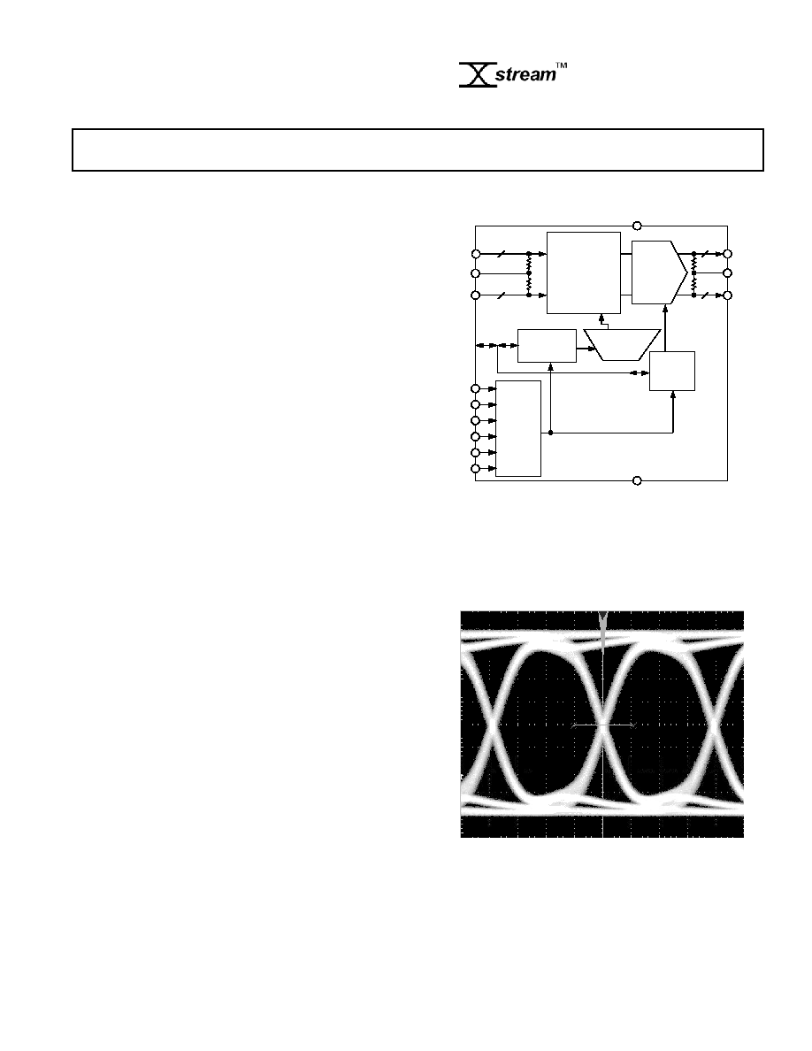
FUNCTIONAL BLOCK DIAGRAM
OUTPUT
LEVEL
DACs
OUTN
OUTP
VTTO
34 34
DIFFERENTIAL
SWITCH MATRIX
34
34
MATRIX
CONNECTION
LATCHES
CONNECTION
DECODE
OUTPUT
LEVEL
LATCHES
CONTROL
LOGIC
INN
VTTI
INP
D[5:0]
A[6:0]
RE
WE
RESET
CS
UPDATE
VEE
VCC
AD8152
34
34
GENERAL DESCRIPTION
AD8152 is a member of the Xstream line of products and is a
breakthrough in digital switching, offering a large switch array
(34
× 34) on very little power, typically 2.0 W. Additionally, it
operates at data rates up to 3.2 Gbps per port, making it suitable
for Sonet/SDH OC-48 with Forward Error Correction (FEC).
The AD8152's useful supply voltage range allows the user to
operate at LVPECL/CML data levels down to 2.5 V. The control
interface is LVTTL or LVCMOS compatible on 2.5 V to 3.3 V.
The AD8152's fully differential signal path reduces jitter and
crosstalk while allowing the use of smaller single-ended voltage
swings. It is offered in a 256-ball SBGA package that operates
over the industrial temperature range of 0
°C to 85°C.
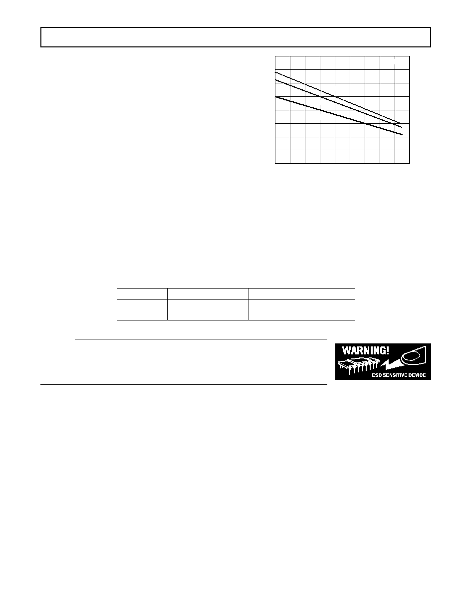
80ps/DIV
100mV/DIV
Figure 1. Eye Pattern, 3.2 Gbps, PRBS 23

REV. A
2
AD8152
(@ 25 C, VCC = 2.5 V to 3.3 V, VEE
= 0 V, R
L
= 50 , Differential Output Swing = 800 mV p-p,
unless otherwise noted.)
Parameter
Condition
Min
Typ
Max
Unit
DYNAMIC PERFORMANCE
Max Data Rate/Channel (NRZ)
3.2
Gbps
Channel Jitter
Data Rate
£ 3.2 Gbps; PRBS 2
23
1
45
ps p-p
RMS Channel Jitter
<10
ps
Propagation Delay
Input to Output
660
800
ps
Propagation Delay Match
±50
±120
ps
Output Rise/Fall Time
20% to 80%
100
ps
INPUT CHARACTERISTICS
Input Voltage Swing
Single-Ended (See TPC 14)
50
1000
mV p-p
Input Voltage Range
Common-Mode (See TPC 15)
VEE + 0.8
VCC + 0.2
V
Input Bias Current
2
mA
Input Capacitance
2
pF
OUTPUT CHARACTERISTICS
Output Voltage Swing
Differential (See TPC 18)
100
800
1600
mV p-p
Output Voltage Range
VCC 1.2
VCC + 0.2
V
Output Current
2
32
mA
Output Capacitance
2
pF
TERMINATION CHARACTERISTICS
Resistance
43
50
57
W
Temperature Coefficient
0.05
W/C
POWER SUPPLY
Operating Range
VCC
VEE = 0 V
2.25
3.63
V
Quiescent Current
VCC
All Outputs Disabled
32
45
mA
All Outputs Enabled
190
mA
VEE
All Outputs Disabled
32
45
mA
All Outputs Enabled
770
mA
T
MIN
to T
MAX,
All Outputs Enabled
800
mA
LOGIC INPUT CHARACTERISTICS
Input High (VIH)
VCC = 3.3 V
2
V
Input Low (VIL)
VCC = 3.3 V
0.8
V
Input High (VIH)
VCC = 2.5 V
1.7
V
Input Low (VIL)
VCC = 2.5 V
0.7
V
LOGIC OUTPUT CHARACTERISTICS
Output High (VOH)
VCC = 3.3 V, IOH = 2 mA
2.4
V
Output Low (VOL)
VCC = 3.3 V, IOL = +2 mA
0.4
V
Output High (VOH)
VCC = 2.5 V, IOH = 100 uA
2.1
V
Output Low (VOL)
VCC = 2.5 V, IOL = +100 uA
0.2
V
THERMAL CHARACTERISTICS
Operating Temperature Range
0
85
C
JA
Still Air
15
C/W
200 lfpm
12
C/W
400 lfpm
11
C/W
Specifications subject to change without notice.
ELECTRICAL CHARACTERISTICS
REV. A
AD8152
3
CAUTION
ESD (electrostatic discharge) sensitive device. Electrostatic charges as high as 4000 V readily
accumulate on the human body and test equipment and can discharge without detection. Although the
AD8152 features proprietary ESD protection circuitry, permanent damage may occur on devices
subjected to high energy electrostatic discharges. Therefore, proper ESD precautions are recommended
to avoid performance degradation or loss of functionality.
ABSOLUTE MAXIMUM RATINGS
1
VCC to VEE . . . . . . . . . . . . . . . . . . . . . . . . . . . . . . . . . . 3.7 V
VTTI . . . . . . . . . . . . . . . . . . . . . . . . . . . . . . . . . VCC + 0.6 V
VTTO . . . . . . . . . . . . . . . . . . . . . . . . . . . . . . . . . VCC + 0.6 V
Internal Power Dissipation
2
AD8152 256-Ball SBGA (BP) . . . . . . . . . . . . . . . . . . 8.33 W
Input Voltage . . . . . . . . . . . . . . . . . . . . . . . . . . . . VCC + 0.6 V
Differential Input Voltage . . . . . . . . . . . . . . . . . . . . . . . . 1.7 V
Logic Input Voltage . . . . . . VEE 0.3 V < V
IN
< VCC + 0.6 V
Storage Temperature Range . . . . . . . . . . . . . 65
°C to +125°C
Lead Temperature Range . . . . . . . . . . . . . . . . . . . . . . . 300
°C
NOTES
1
Stresses above those listed under Absolute Maximum Ratings may cause perma-
nent damage to the device. This is a stress rating only; functional operation of the
device at these or any other conditions above those indicated in the operational
sections of this specification is not implied. Exposure to absolute maximum rating
conditions for extended periods may affect device reliability.
2
Specification is for the device in free air (T
A
= 25
°C):
JA
= 15
°C/W @ still air.
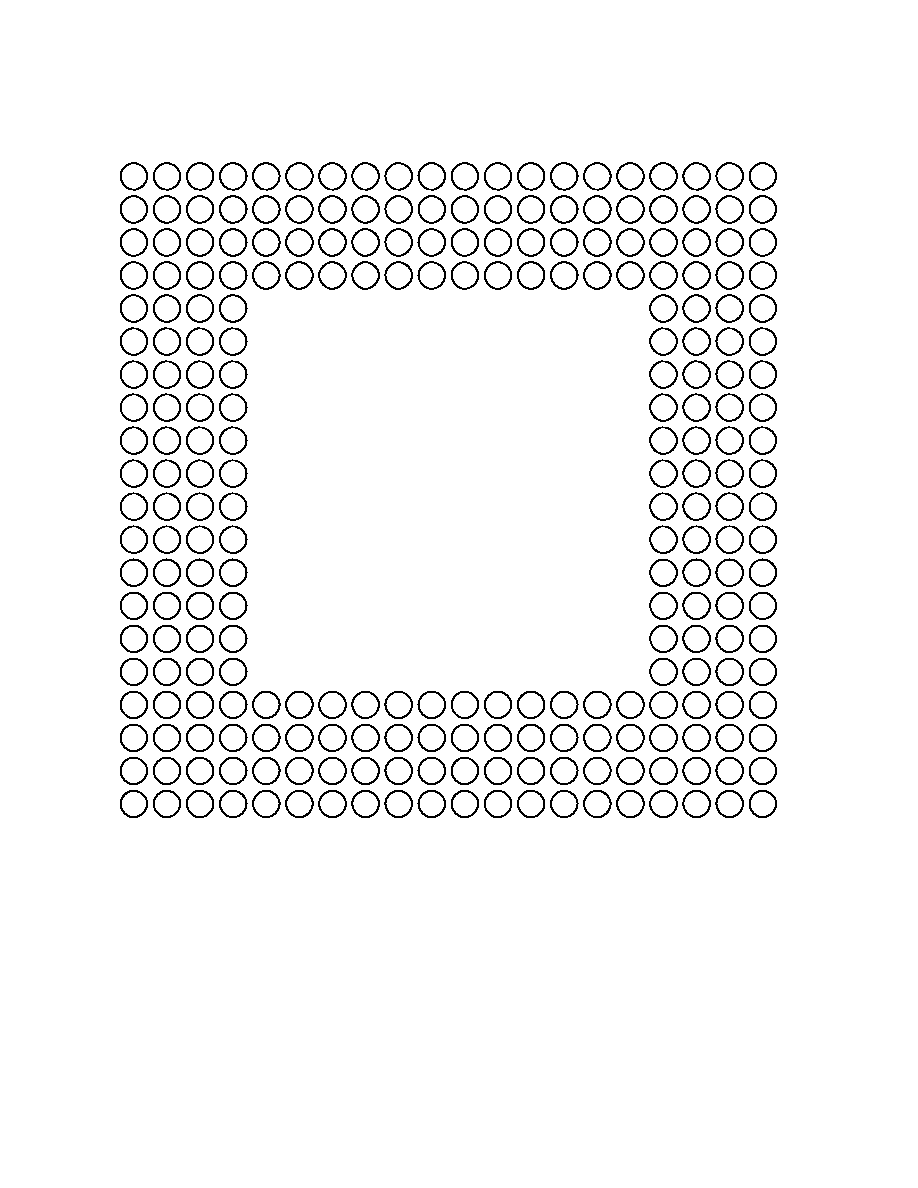
MAXIMUM POWER DISSIPATION
The maximum power that can be safely dissipated by the AD8152 is
limited by the associated rise in junction temperature. The maxi-
mum safe junction temperature for plastic encapsulated devices
is determined by the glass transition temperature of the plastic,
approximately 150
°C. Temporarily exceeding this limit may cause
16
0
0
90
10
20
30
40
50
60
70
80
14
8
6
4
2
12
10
AMBIENT TEMPERATURE C
MAXIMUM PO
WER DISSIP
A
TION
W
Tj = 150 C
400 lfpm
200 lfpm
STILL AIR
Figure 2. Maximum Power Dissipation vs. Temperature
a shift in parametric performance due to a change in the stresses
exerted on the die by the package. Exceeding a junction tem-
perature of 175
°C for an extended period can result in device
failure. To ensure proper operation, it is necessary to observe the
maximum power derating curves shown in Figure 2.
ORDERING GUIDE
Model
Temperature Range
Package Description
AD8152JBP
0
°C to 85°C
256-Ball SBGA (27 mm
× 27 mm)
AD8152-EVAL
Evaluation Board
REV. A
4
AD8152
BALL GRID ARRAY
20
19
18
17
16
15
14
13
12
11
10
9
8
7
6
5
4
3
2
1
A
B
C
D
E
F
G
H
J
K
L
M
N
P
R
T
U
V
W
Y
A
B
C
D
E
F
G
H
J
K
L
M
N
P
R
T
U
V
W
Y
20
19
18
17
16
15
14
13
12
11
10
9
8
7
6
5
4
3
2
1
VEE
VEE
VEE
VEE
VEE
VEE
VEE
VEE
VEE
VEE
VEE
VEE
VEE
VEE
VEE
VEE
VEE
VEE
VEE
VEE
VEE
VEE
VEE
VEE
VEE
VEE
VEE
VEE
VEE
VEE
VEE
VEE
VEE
VEE
VEE
VEE
VEE
VEE
VEE
VEE
VCC
VCC
VCC
VCC
VCC
VCC
VCC
VCC
VCC
VCC
VCC
VCC
VCC
VCC
VCC
VCC
VCC
VCC
VCC
VCC
VCC
VCC
VTTO
VTTO
VTTO
VTTO
VTTO
VTTO
VTTO
VTTO
VTTO
VTTO
VTTO
VTTO
VTTO
VTTO
VTTO
VTTO
VTTO
VTTO
VTTO
VTTO
VTTI
VTTI
VTTI
VTTI
VTTI
VTTI
VTTI
VTTI
VTTI
VTTI
VTTI
VTTI
VTTI
VTTI
VTTI
VTTI
O20P
O21P
O19N
O19P
O18N
O17P
O17N
O18P
O27N
O25P
O25N
O24N
O23P
O23N
O24P
O22P
O22N
O21N
O30N
O29P
O29N
O30P
O28N
O28P
O27P
O26N
O26P
O32P
O32N
O31P
O20N
O31N
O33N
O33P
O00P
O05N
O05P
O04P
O03N
O03P
O01N
O02P
O02N
O01P
O00N
O09P
O09N
O07N
O08N
O08P
O07P
O06N
O06P
O04N
O13N
O14P
O14N
O13P
O12N
O12P
O10P
O11P
O11N
O10N
O16N
O16P
O15N
O15P
I16N
I16P
I15N
I09N
I11N
I11P
I12P
I13N
I13P
I12N
I14N
I14P
I15P
I07P
I06N
I06P
I07N
I08N
I08P
I09P
I10P
I10N
I00N
I01P
I02P
I02N
I04P
I03N
I03P
I04N
I05N
I05P
I01N
I00P
I31N
I33N
I17P
I19P
I20N
I22N
I23N
I25N
I27P
I28N
I30N
I22P
I23P
I25P
I27N
I28P
I30P
I31P
I33P
I17N
I19N
I20P
I24P
I26P
I26N
I29P
I29N
I32P
I32N
I24N
I21N
I21P
I18P
I18N
D1
RESET
D2
D3
D0
CS
RE
D5
D4
UPDATE
A0
WE
A1
A2
A5
A6
A4
A3
N/C
N/C
N/C
N/C
Ball Diagram, View from the Bottom
REV. A
AD8152
5
Ball Mnemonic Type
Description
A1
VEE
Power
Negative Supply
A2
VEE
Power
Negative Supply
A3
VEE
Power
Negative Supply
A4
VCC
Power
Positive Supply
A5
VTTO
Power
Output Termination Supply
A6
OUT02P
I/O
High Speed Output
A7
VTTO
Power
Output Termination Supply
A8
OUT05P
I/O
High Speed Output
A9
VTTO
Power
Output Termination Supply
A10 OUT08P
I/O
High Speed Output
A11 VCC
Power
Positive Supply
A12 OUT11P
I/O
High Speed Output
A13 VTTO
Power
Output Termination Supply
A14 OUT14P
I/O
High Speed Output
A15 VTTO
Power
Output Termination Supply
A16 VCC
Power
Positive Supply
A17 VEE
Power
Negative Supply
A18 VEE
Power
Negative Supply
A19 VEE
Power
Negative Supply
A20 VEE
Power
Negative Supply
B1
VEE
Power
Negative Supply
B2
VEE
Power
Negative Supply
B3
VEE
Power
Negative Supply
B4
VCC
Power
Positive Supply
B5
VTTO
Power
Output Termination Supply
B6
OUT02N
I/O
High Speed Output Complement
B7
VTTO
Power
Output Termination Supply
B8
OUT05N
I/O
High Speed Output Complement
B9
VTTO
Power
Output Termination Supply
B10 OUT08N
I/O
High Speed Output Complement
B11 VCC
Power
Positive Supply
B12 OUT11N
I/O
High Speed Output Complement
B13 VTTO
Power
Output Termination Supply
B14 OUT14N
I/O
High Speed Output Complement
B15 VTTO
Power
Output Termination Supply
B16 VCC
Power
Positive Supply
B17 VEE
Power
Negative Supply
B18 VEE
Power
Negative Supply
B19 VEE
Power
Negative Supply
B20 VEE
Power
Negative Supply
C1
VEE
Power
Negative Supply
C2
VEE
Power
Negative Supply
C3
A5
Control Output Address Pin (MSB)
C4
A6
Control Output Address Pin (Bank Des.)
C5
OUT00P
I/O
High Speed Output
C6
OUT01N
I/O
High Speed Output Complement
C7
OUT03P
I/O
High Speed Output
C8
OUT04N
I/O
High Speed Output Complement
C9
OUT06P
I/O
High Speed Output
C10 OUT07N
I/O
High Speed Output Complement
C11 OUT09P
I/O
High Speed Output
Ball Mnemonic
Type
Description
C12 OUT10N
I/O
High Speed Output Complement
C13 OUT12P
I/O
High Speed Output
C14 OUT13N
I/O
High Speed Output Complement
C15 OUT15P
I/O
High Speed Output
C16 OUT16N
I/O
High Speed Output Complement
C17 D5
Control Input Address Pin (MSB)
C18 D4
Control Input Address Pin
C19 VEE
Power
Negative Supply
C20 VEE
Power
Negative Supply
D1
A1
Control Output Address Pin
D2
A2
Control Output Address Pin
D3
A3
Control Output Address Pin
D4
A4
Control Output Address Pin
D5
OUT00N
I/O
High Speed Output Complement
D6
OUT01P
I/O
High Speed Output
D7
OUT03N
I/O
High Speed Output Complement
D8
OUT04P
I/O
High Speed Output
D9
OUT06N
I/O
High Speed Output Complement
D10 OUT07P
I/O
High Speed Output
D11 OUT09N
I/O
High Speed Output Complement
D12 OUT10P
I/O
High Speed Output
D13 OUT12N
I/O
High Speed Output Complement
D14 OUT13P
I/O
High Speed Output
D15 OUT15N
I/O
High Speed Output Complement
D16 OUT16P
I/O
High Speed Output
D17 D3
Control Input Address Pin
D18 D2
Control Input Address Pin
D19 D1
Control Input Address Pin
D20 D0
Control Input Address Pin (LSB)
E1
A0
Control Output Address Pin (LSB)
E2
UPDATE
Control Second Rank Write Enable
E3
N/C Reserved
Do Not Connect
E4
N/C Reserved
Do Not Connect
E17 N/C Reserved
Do Not Connect
E18 N/C Reserved
Do Not Connect
E19
RESET
Control Reset/Disable Outputs
E20
CS
Control Chip Select Enable
F1
VCC
Power
Positive Supply
F2
WE
Control First Rank Write Enable
F3
IN00P
I/O
High Speed Input
F4
IN00N
I/O
High Speed Input Complement
F17 IN17N
I/O
High Speed Input Complement
F18 IN17P
I/O
High Speed Input
F19
RE
Control Readback Enable
F20 VCC
Power
Positive Supply
G1
IN02P
I/O
High Speed Input
G2
IN02N
I/O
High Speed Input Complement
G3
IN01N
I/O
High Speed Input Complement
G4
IN01P
I/O
High Speed Input
G17 IN18P
I/O
High Speed Input
G18 IN18N
I/O
High Speed Input Complement
BALL GRID DESCRIPTIONS
REV. A
6
AD8152
Ball Mnemonic Type
Description
G19 IN19N
I/O
High Speed Input Complement
G20 IN19P
I/O
High Speed Input
H1
VTTI
Power
Input Termination Supply
H2
VTTI
Power
Input Termination Supply
H3
IN03P
I/O
High Speed Input
H4
IN03N
I/O
High Speed Input Complement
H17 IN20N
I/O
High Speed Input Complement
H18 IN20P
I/O
High Speed Input
H19 VTTI
Power
Input Termination Supply
H20 VTTI
Power
Input Termination Supply
J1
IN05P
I/O
High Speed Input
J2
IN05N
I/O
High Speed Input Complement
J3
IN04N
I/O
High Speed Input Complement
J4
IN04P
I/O
High Speed Input
J17
IN21P
I/O
High Speed Input
J18
IN21N
I/O
High Speed Input Complement
J19
IN22N
I/O
High Speed Input Complement
J20
IN22P
I/O
High Speed Input
K1
VTTI
Power
Input Termination Supply
K2
VTTI
Power
Input Termination Supply
K3
IN06P
I/O
High Speed Input Complement
K4
IN06N
I/O
High Speed Input
K17 IN23N
I/O
High Speed Input Complement
K18 IN23P
I/O
High Speed Input
K19 VTTI
Power
Input Termination Supply
K20 VTTI
Power
Input Termination Supply
L1
IN08P
I/O
High Speed Input
L2
IN08N
I/O
High Speed Input Complement
L3
IN07N
I/O
High Speed Input Complement
L4
IN07P
I/O
High Speed Input
L17 IN24P
I/O
High Speed Input
L18 IN24N
I/O
High Speed Input Complement
L19 IN25N
I/O
High Speed Input Complement
L20 IN25P
I/O
High Speed Input
M1
VCC
Power
Positive Supply
M2
VCC
Power
Positive Supply
M3
IN09P
I/O
High Speed Input
M4
IN09N
I/O
High Speed Input Complement
M17 IN26N
I/O
High Speed Input Complement
M18 IN26P
I/O
High Speed Input
M19 VCC
Power
Positive Supply
M20 VCC
Power
Positive Supply
N1
IN11P
I/O
High Speed Input
N2
IN11N
I/O
High Speed Input Complement
N3
IN10N
I/O
High Speed Input Complement
N4
IN10P
I/O
High Speed Input
N17 IN27P
I/O
High Speed Input
N18 IN27N
I/O
High Speed Input Complement
N19 IN28N
I/O
High Speed Input Complement
N20 IN28P
I/O
High Speed Input
P1
VTTI
Power
Input Termination Supply
Ball Mnemonic Type
Description
P2
VTTI
Power
Input Termination Supply
P3
IN12P
I/O
High Speed Input
P4
IN12N
I/O
High Speed Input Complement
P17
IN29N
I/O
High Speed Input Complement
P18
IN29P
I/O
High Speed Input
P19
VTTI
Power
Input Termination Supply
P20
VTTI
Power
Input Termination Supply
R1
IN14P
I/O
High Speed Input
R2
IN14N
I/O
High Speed Input Complement
R3
IN13N
I/O
High Speed Input Complement
R4
IN13P
I/O
High Speed Input
R17 IN30P
I/O
High Speed Input
R18 IN30N
I/O
High Speed Input Complement
R19 IN31N
I/O
High Speed Input Complement
R20 IN31P
I/O
High Speed Input
T1
VTTI
Power
Input Termination Supply
T2
VTTI
Power
Input Termination Supply
T3
IN15P
I/O
High Speed Input
T4
IN15N
I/O
High Speed Input Complement
T17 IN32N
I/O
High Speed Input Complement
T18 IN32P
I/O
High Speed Input
T19 VTTI
Power
Input Termination Supply
T20 VTTI
Power
Input Termination Supply
U1
VCC
Power
Positive Supply
U2
VCC
Power
Positive Supply
U3
IN16N
I/O
High Speed Input Complement
U4
IN16P
I/O
High Speed Input
U5
OUT17N
I/O
High Speed Output Complement
U6
OUT18P
I/O
High Speed Output
U7
OUT20N
I/O
High Speed Output Complement
U8
OUT21P
I/O
High Speed Output
U9
OUT23N
I/O
High Speed Output Complement
U10 OUT24P
I/O
High Speed Output
U11 OUT26N
I/O
High Speed Output Complement
U12 OUT27P
I/O
High Speed Output
U13 OUT29N
I/O
High Speed Output
U14 OUT30P
I/O
High Speed Output
U15 OUT32N
I/O
High Speed Output Complement
U16 OUT33P
I/O
High Speed Output
U17 IN33P
I/O
High Speed Input
U18 IN33N
I/O
High Speed Input Complement
U19 VCC
Power
Positive Supply
U20 VCC
Power
Positive Supply
V1
VEE
Power
Negative Supply
V2
VEE
Power
Negative Supply
V3
VEE
Power
Negative Supply
V4
VEE
Power
Negative Supply
V5
OUT17P
I/O
High Speed Output
V6
OUT18N
I/O
High Speed Output Complement
V7
OUT20P
I/O
High Speed Output
V8
OUT21N
I/O
High Speed Output Complement
BALL GRID DESCRIPTIONS (continued)
REV. A
AD8152
7
Ball Mnemonic Type
Description
V9
OUT23P
I/O
High Speed Output
V10 OUT24N
I/O
High Speed Output Complement
V11 OUT26P
I/O
High Speed Output
V12 OUT27N
I/O
High Speed Output Complement
V13 OUT29P
I/O
High Speed Output
V14 OUT30N
I/O
High Speed Output Complement
V15 OUT32P
I/O
High Speed Output
V16 OUT33N
I/O
High Speed Output Complement
V17 VEE
Power
Negative Supply
V18 VEE
Power
Negative Supply
V19 VEE
Power
Negative Supply
V20 VEE
Power
Negative Supply
W1
VEE
Power
Negative Supply
W2
VEE
Power
Negative Supply
W3
VEE
Power
Negative Supply
W4
VCC
Power
Positive Supply
W5
VTTO
Power
Output Termination Supply
W6
OUT19N
I/O
High Speed Output Complement
W7
VTTO
Power
Output Termination Supply
W8
OUT22N
I/O
High Speed Output Complement
W9
VTTO
Power
Output Termination Supply
W10 OUT25N
I/O
High Speed Output Complement
W11 VCC
Power
Positive Supply
W12 OUT28N
I/O
High Speed Output Complement
W13 VTTO
Power
Output Termination Supply
W14 OUT31N
I/O
High Speed Output Complement
Ball Mnemonic Type
Description
W15 VTTO
Power
Output Termination Supply
W16 VCC
Power
Positive Supply
W17 VEE
Power
Negative Supply
W18 VEE
Power
Negative Supply
W19 VEE
Power
Negative Supply
W20 VEE
Power
Negative Supply
Y1
VEE
Power
Negative Supply
Y2
VEE
Power
Negative Supply
Y3
VEE
Power
Negative Supply
Y4
VCC
Power
Positive Supply
Y5
VTTO
Power
Output Termination Supply
Y6
OUT19P
I/O
High Speed Output
Y7
VTTO
Power
Output Termination Supply
Y8
OUT22P
I/O
High Speed Output
Y9
VTTO
Power
Output Termination Supply
Y10 OUT25P
I/O
High Speed Output
Y11 VCC
Power
Positive Supply
Y12 OUT28P
I/O
High Speed Output
Y13 VTTO
Power
Output Termination Supply
Y14 OUT31P
I/O
High Speed Output
Y15 VTTO
Power
Output Termination Supply
Y16 VCC
Power
Positive Supply
Y17 VEE
Power
Negative Supply
Y18 VEE
Power
Negative Supply
Y19 VEE
Power
Negative Supply
Y20 VEE
Power
Negative Supply
BALL GRID DESCRIPTIONS (continued)
REV. A
8
AD8152Typical Performance Characteristics
80ps/DIV
100mV/DIV
TPC 1. Eye Pattern 3.2 Gbps
100mV/DIV
20ps/DIV
PEAK-PEAK JITTER = 35ps STD DEV = 5.1ps
TPC 2. Jitter @ 3.2 Gbps
100mV/DIV
1.2ns/DIV
TPC 3. Response, 3.2 Gbps, 32-Bit Pattern
1111 1111 0000 0000 1010 1010 1100 1100
100mV/DIV
200ps/DIV
TPC 4. Eye Pattern 1.5 Gbps
100mV/DIV
20ps/DIV
PEAK-PEAK JITTER = 35ps STD DEV = 5.2ps
TPC 5. Jitter @ 1.5 Gbps
100mV/DIV
2.5ns/DIV
TPC 6. Response, 1.5 Gbps, 32-Bit Pattern
1111 1111 0000 0000 1010 1010 1100 1100
(2.5 V Supply, VCC
= VTTI = VTTO, Data Rate = 3.2 Gbps;
PRBS 2
23
1; Differential Output Swing = 800 mV p-p; R
L
= 50
; Input Amplitude = 0.4 V p-p Single-Ended; unless otherwise noted.)
REV. A
AD8152
9
DUTY CYCLE DISTORTION ps
1400
800
0
50
30
FREQ
UENCY
0
20
1200
1000
600
400
40
50
BIN WIDTH = 5ps
200
40
20
30
10
10
TPC 7. Duty Cycle Distortion Distribution
DATA RATE Gbps
100
90
0
0.5
4.0
1.0
EYE HEIGHT %
1.5
2.0
2.5
3.0
3.5
80
70
60
50
40
30
20
10
V
OUT
@ DATA RATE
V
OUT
@ 0.5Gbps
100
%EYE HEIGHT =
TPC 8. Eye Height vs. Data Rate
DATA RATE Gbps
50
4.0
1.0
JITTER ps
1.5
2.0
2.5
3.0
3.5
45
40
35
30
25
15
10
5
0
PEAK-PEAK JITTER
STANDARD DEVIATION
20
TPC 9. Jitter vs. Data Rate
UNIT INTERVAL
1.E+00
0.1
0.5
BIT ERR
OR RA
TE
0.4
0.3
0.2
0.1
0
0.2
0.3
0.4
0.5
1.E01
1.E02
1.E03
1.E04
1.E05
1.E06
1.E07
1.E08
1.E09
1.E10
1.E11
1.E12
TPC 10. Bit Error Rate vs. Unit Interval
100mV/DIV
80ps/DIV
PEAK-PEAK JITTER = 35ps STD DEV = 5.6ps
TPC 11. Crosstalk, 3.2 Gbps, Attack Signal OFF
(See TPC 25)
100mV/DIV
80ps/DIV
PEAK-PEAK JITTER = 46ps STD DEV = 6.5ps
TPC 12. Crosstalk, 3.2 Gbps, Attack Signal ON
(See TPC 25)
REV. A
10
AD8152
TEMPERATURE C
50
50
0
PEAK-PEAK JITTER ps
10
20
30
40
45
40
35
30
25
60
70
80
90
55
3.2 Gbps
1.5 Gbps
TPC 13. Single Point Jitter vs. Temperature
INPUT AMPLITUDE mV
0
JITTER ps
10
100
1000
STANDARD DEVIATION
PEAKPEAK JITTER
120
100
80
60
40
20
0
TPC 14. Jitter vs. Single-Ended Input Amplitude
INPUT CML V
160
PEAK-PEAK JITTER ps
140
120
100
80
60
180
40
20
3.8
3.2
2.9
2.6
2.3
2.0
1.7
1.4
1.1
0.8
0.5
3.5
INPUT AMPLITUDE = 50mV p-p
@3.3V
@2.5V
TPC 15. Jitter vs. Input Common-Mode Level
SUPPLY VOLTAGE V
JITTER ps
80
70
60
50
4.0
3.6
3.4
3.2
3.0
2.8
2.6
2.4
2.2
2.0
1.8
3.8
40
30
20
10
0
STANDARD DEVIATION
PEAK-PEAK JITTER
TPC 16. Jitter vs. Supply
V
OL
V
PEAK-PEAK JITTER ps
1.4
0
160
140
120
100
80
60
40
20
1.2
1.0
0.6
0.4
0.2
0
I
OUT
= 16mA
I
OUT
= 24mA
I
OUT
= 32mA
0.8
TPC 17. Jitter vs. V
OL
(Relative to VCC)
I
OUT
mA
JITTER ps
0
10
50
45
40
35
30
25
20
15
PEAKPEAK JITTER
STANDARD DEVIATION
5
10
15
20
25
30
35
5
0
TPC 18. Jitter vs. Programmed I
OUT
REV. A
AD8152
11
PROPAGATION DELAY ps
FREQ
UENCY
600
0
160
140
120
100
80
60
40
20
BIN WIDTH = 5ps
625
650
675
700
725
750
TPC 19. Variation in Propagation Delay
740
780
760
800
660
720
700
680
640
620
600
PR
OP
A
G
A
T
ION DELA
Y ps
TEMPERATURE C
40
30
20
10
0
50
60
70
80
90
TPC 20. Propagation Delay vs. Temperature
SUPPLY VOLTAGE V
725
PR
OP
A
G
A
T
ION DELA
Y ps 700
675
650
625
600
750
2.8
2.6
2.4
2.2
2.0
3.0
3.2
3.4
3.6
3.8
TPC 21. Propagation Delay vs. Supply
I
OUT
CODE
I
OUT
mA
MEASURED
IDEAL
0
1
2
3
4
5
6
7
8
9
0
2
4
6
8
10 11 12 13 14 15 16
10
12
14
16
18
20
22
24
26
28
32
30
34
TPC 22. I
OUT
vs. I
OUT
Code
REV. A
12
AD8152
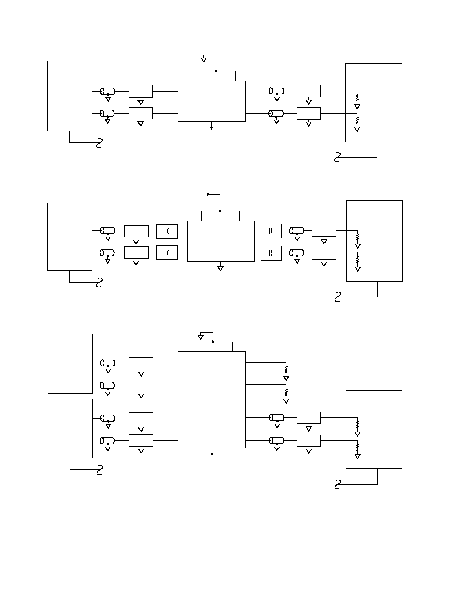
AD8152
IN##P
OUT##P
IN##N
OUT##N
VEE
= 2.5V
I
OUT
= 16mA, V
OUT
HI = 0V, V
OUT
LO = 0.4V
V
IN
AMPLITUDE = 400mV p-p SINGLE-ENDED, V
IN
HI = 0.2V PRBS 2
23
1
PATTERN
GENERATOR
VCC
VTTO
VTTI
50
50
DATA OUT
DATA OUT
TRIGGER OUT
TRIGGER IN
HIGH SPEED
SAMPLING
OSCILLOSCOPE
6dB
6dB
6dB
6dB
TPC 23. Negative Supply Test Circuit
I
OUT
= 16mA, V
OUT
HI = 2.5V, V
OUT
LO = 2.1V
V
IN
AMPLITUDE = 400mV p-p SINGLE-ENDED, V
IN
HI = 2.7V
PRBS 2
23
1, INPUTS AND OUTPUTS ARE AC-COUPLED
PATTERN
GENERATOR
VCC
VTTO
2.5V
VTTI
50
50
DATA OUT
DATA OUT
TRIGGER OUT
TRIGGER IN
HIGH SPEED
SAMPLING
OSCILLOSCOPE
6dB
6dB
VEE
6dB
6dB
AD8152
IN##P
OUT##P
IN##N
OUT##N
0.1 F
0.1 F
0.1 F
0.1 F
TPC 24. Positive Supply Test Circuit
ATTACK SIGNAL APPLIED TO IN25. IN25 BROADCAST TO ALL OUTPUTS EXCEPT OUT27.
TWO SEPARATE PATTERN GENERATORS USED TO PROVIDE INPUT PATTERN TO AD8152.
OUTPUTS NOT CONNECTED TO OSCILLOSCOPE ARE TERMINATED WITH EXTERNAL 50 TO GND.
50
50
6dB
6dB
6dB
6dB
AD8152
VEE
= 2.5V
PATTERN
GENERATOR #2
DATA OUT
DATA OUT
VCC
VTTO
VTTI
TRIGGER OUT
TRIGGER IN
HIGH SPEED
SAMPLING
OSCILLOSCOPE
IN24N
IN24P
OUT27P
OUT27N
IN25N
IN25P
OUT00P...OUT26P
OUT28P...OUT33P
OUT00N...OUT26N
OUT28N...OUT33N
50
50
6dB
6dB
PATTERN
GENERATOR #1
ATTACK SIGNAL
DATA OUT
DATA OUT
TPC 25. Crosstalk Test Circuit
REV. A
AD8152
13
Table I. Address and Data Buses
Connection/Current Bit
Output Address Pins
Data Pins
A6
A5
A4
A3
A2
A1
A0
D5
D4
D3
D2
D1
D0
0 = CONNECTION LATCHES
1 = OUTPUT CURRENT LEVEL
MSB
LSB
MSB
LSB
Table II. Connection Data and Address Programming Examples
Connection/
Data Pins
Current Bit
Output Address Pins
(Used to Select Inputs)
Comments
0 = CONNECTION
MSB
LSB
MSB
LSB
A6
A5 A4 A3 A2 A1 A0
D5 D4 D3 D2 D1 D0
0
0
0
0
0
0
0
0
0
0
0
0
0
Program IN00 to OUT00
0
0
0
0
0
0
0
1
0
0
0
0
1
Program IN33 to OUT00
0
1
0
0
0
0
1
0
1
1
1
1
1
Program IN31 to OUT33
0
1
1
1
1
1
1
0
0
0
0
0
0
Broadcast IN00 to All Outputs
0
0
0
0
0
0
0
1
1
1
1
1
1
Disable OUT00
0
1
0
0
0
0
1
1
1
1
1
1
1
Disable OUT33
0
1
1
1
1
1
1
1
1
1
1
1
1
Disable All Outputs (Broadcast)
Table III. Output-Current Level Data and Address Programming Examples
Connection/
Data Pins
Current Bit
Output Address Pins
(Used to Select Inputs)
Comments
1 = CURRENT LEVEL MSB
LSB MSB
LSB
A6
A5 A4
A3 A2 A1 A0
D5
D4
D3
D2 D1 D0
1
0
0
0
0
0
0
X
X
0
0
0
0
Program OUT00 to Current--Code 00 (2 mA)
1
0
0
0
0
0
0
X
X
1
1
1
1
Program OUT00 to Current--Code 15 (32 mA)
1
1
0
0
0
0
1
X
X
0
1
1
1
Program OUT33 to Current--Code 07 (16 mA)
1
1
1
1
1
1
1
X
X
1
0
0
0
Broadcast Current--Code 08 to All
Outputs (18 mA)
Table IV. Basic Control Strobe Functions
RESET CS
WE
RE
UPD Function
0
X
X
X
X
Global Reset. Disables all outputs and resets all output current to code 0111 (16 mA).
1
1
X
X
X
Disable All Control Signals. Signal matrix/currents remain the same. D5:D0 are high impedance.
1
0
0
1
X
Write Enable. Write D5:D0 data into first rank register addressed by A6:A0.
1
0
X
0
X
Single-Output Readback. Second rank register data for output A6:A0 appears on D5:D0.
1
0
X
X
0
Global Update. Copy all first rank data into second rank registers.
1
0
0
1
0
Transparent Write and Update. D5:D0 immediately control programming. Use
RE as gating signal.
REV. A
14
AD8152
CS
WE
A[6:0]INPUTS
D[5:0]INPUTS
t
CSW
t
ASW
t
WP
t
DSW
t
AHW
t
AHW
t
CHW
t
DHW
Figure 3a. First Rank Write Cycle
Table V. First Rank Write Cycle
Symbol
Parameter
Conditions
Min
Typ
Max
Unit
t
CSW
Setup Time
Chip Select to Write Enable
T
A
= 25 C
0
ns
t
ASW
Address to Write Enable
0
ns
t
DSW
Data to Write Enable
VCC = 3.3 V
1
ns
t
CHW
Hold Time
Chip Select from Write Enable
0
ns
t
AHW
Address from Write Enable
0
ns
t
DHW
Data from Write Enable
0
ns
t
WP
Width of Write Enable Pulse
10
ns
CS
UPDATE
ENABLING
OUT[0:33][N:P]
OUTPUTS
TOGGLE
OUT[0:33][N:P]
OUTPUTS
DATA FROM RANK 1
t
CSU
t
UOE
t
UW
t
CHU
DISABLING
OUT[0:33][N:P]
OUTPUTS
t
UOD
DATA FROM RANK 1
DATA FROM RANK 2
PREVIOUS RANK 2 DATA
t
UOT
Figure 3b. Second Rank Update Cycle
Table VI. Second Rank Update Cycle
Symbol
Parameter
Conditions
Min
Typ
Max
Unit
t
CSU
Setup Time
Chip Select to Update
T
A
= 25 C
0
ns
t
CHU
Hold Time
Chip Select from Update
0
ns
t
UOE
Output Enable Times
Update to Output Enable
VCC = 3.3 V
25
45
ns
t
UOT
Output Toggle Times
Update to Output Reprogram
25
45
ns
t
UOD
Output Disable Times
Update to Output Disabled
25
45
ns
t
UW
Width of Update Pulse
10
ns
REV. A
AD8152
15
CS
UPDATE
INPUT {DATA 1}
WE
ENABLING
OUT[0:33][N:P]
OUTPUTS
DISABLING
OUT[0:33][N:P]
OUTPUTS
INPUT {DATA 1}
INPUT {DATA 0}
t
CSU
t
UOT
t
UOE
t
UW
t
WOT
t
WOD
t
WHU
t
CHU
INPUT {DATA 2}
Figure 4a. Transparent Write and Update Cycle
Table VII. Transparent Update Cycle
Symbol
Parameter
Conditions
Min
Typ
Max
Unit
t
CSU
Setup Time
Chip Select to Update
T
A
= 25 C
0
ns
t
CHU
Hold Time
Chip Select from Update
VCC = 3.3 V
0
ns
t
UOE
Output Enable Times
Update to Output Enable
35
50
ns
t
WOE
*
Write Enable to Output Enable
35
50
ns
t
UOT
Output Toggle Times
Update to Output Reprogram
25
45
ns
t
WOT
Write Enable to Output Reprogram
25
45
ns
t
UOD
*
Output Disable Times
Update to Output Disabled
25
45
ns
t
WOD
Write Enable to Output Disabled
25
45
ns
t
WHU
Setup Time
Write Enable to Update
0
ns
t
UW
Width of Update Pulse
10
ns
*Not shown
CS
RE
INPUT
D[5:0]
A[5:0]
OUTPUTS
ADDR 1
ADDR 2
{ADDR 1}
DATA
DATA {ADDR 2}
t
AA
t
RDE
t
CSR
t
RHA
t
CHR
t
RDD
Figure 4b. Second Rank Readback Cycle
Table VIII. Second Rank Readback Cycle
Symbol
Parameter
Conditions
Min
Typ
Max
Unit
t
CSR
Setup Time
Chip Select to Read Enable
T
A
= 25 C
0
ns
t
CHR
Hold Time
Chip Select from Read Enable
VCC = 3.3 V
0
ns
t
RHA
Address from Read Enable
5
ns
t
RDE
Enable Time
Data from Read Enable
15
ns
t
AA
Access Time
Data from Address
15
30
ns
REV. A
16
AD8152
RESET
DISABLING
OUT[0:33][N:P]
OUTPUTS
t
TOD
t
TW
Figure 5. Asynchronous Reset
Table IX. Asynchronous Reset
Symbol
Parameter
Conditions
Min
Typ
Max
Unit
t
TOD
Disable Time
Output Disable from Reset
T
A
= 25 C
10
25
ns
t
TW
Width of Reset Pulse
VCC = 3.3 V
10
ns
CONTROL INTERFACE
The AD8152 control interface receives and stores the desired
connection matrix and output levels for the 34 input and 34 output
signal pairs. The interface consists of 34 rows of double-rank
6-bit latches, one for each output. The 6-bit data-word stored
in these latches indicates to which (if any) of the 34 inputs the
output will be connected, as well as the full-scale output current.
One output at a time can be preprogrammed by addressing the
output and writing the desired connection data or output cur-
rent into the first rank of latches. This process can be repeated
until each of the desired output changes has been preprogrammed.
All output connections can then be programmed at once by passing
the data from the first rank of latches into the second rank. The
output connections always reflect the data programmed into the
second rank of latches and do not change until the first rank of
data is passed into the second rank.
If necessary for system verification, the data in the second rank
of latches can be read back from the control interface.
At any time, a reset pulse can be applied to the control interface to
globally reset the appropriate second rank data bits, disabling all 34
signal output pairs and resetting the output currents. To facilitate
multiple chip address decoding, there is a chip select pin. All logic
signals except the reset pulse are ignored unless the chip select
pin is active. The chip select pin disables only the control logic
interface and does not change the operation of the signal matrix.
The chip select pin does not power down any of the latches, so any
data programmed in the latches is preserved.
All control pins are level-sensitive, not edge-triggered.
CONTROL PIN DESCRIPTION
A[6:0] Inputs
Output address pins. The binary encoded address applied to the
lower A[5:0] input pins determines which of the 34 outputs is
being programmed (or being read back). The most significant bit,
A6, determines whether the data pins contain information for
the connection register bank or the output level register bank.
Using the broadcast address, A[5:0] = "111111" will simulta-
neously program data into all outputs at once.
D[5:0] Inputs/Outputs
Input configuration or output level data pins. In write mode,
when the bank selection bit A6 is LOW, the binary encoded data
applied to pins D[5:0] determine which of the 34 inputs is to be
connected to the output specified with the A[5:0] pins. The most
significant bit is D5, and the least significant bit is D0. To disable
an output completely, the input address D[5:0] = "111111"
should be written into the input configuration bank at the desired
output address.
In write mode, when the bank selection bit A6 is HIGH, the
binary encoded data applied to pins D[3:0] indicate the output
current level to be used for the output specified with the A[5:0]
pins. The reset default is "0111" for 16 mA. Each LSB is 2 mA.
In readback mode, pins D[5:0] are low impedance outputs
indicating the data-word stored in the second rank for the out-
put specified with the A[5:0] pins and the bank specified with
the A6 bit. The readback drivers were designed to drive high
impedances only, so external drivers connected to the D[5:0]
should be disabled during readback mode.
WE Input
First rank write enable. Forcing this pin to logic low allows the
data on pins D[5:0] to be stored in the first rank latch for the
output specified by pins A[6:0]. The
WE pin must be returned to a
logic high state after a write cycle to avoid overwriting the first
rank data.
UPDATE Input
Second rank write enable. Forcing this pin to logic low allows the
data stored in all 34 first rank latches (in both banks) to be trans-
ferred to the second rank latches. The signal connection matrix
will be reprogrammed when the second rank data and levels are
changed. This is a global pin, transferring all 34 rows of data at
once. It is not necessary to program the address pins. It should
be noted that after initial power-up of the device, the first rank
data is undefined. It is desirable to preprogram all 17 outputs
before performing the first update cycle.
RE Input
Second rank read enable. Forcing this pin to logic low enables the
output drivers on the bidirectional D[5:0] pins, entering the read-
back mode of operation. By selecting an output address with the
A[6:0] pins and forcing
RE to logic low, the 6-bit data stored in
the second rank latch for that output address will be written to
D[5:0] pins. Data should not be written to the D[5:0] pins
externally while in readback mode. The
RE is a higher priority
pin than the
WE pin, so first rank programming is not possible
while in readback mode.
REV. A
AD8152
17
CS Input
Chip select. This pin must be forced to logic low to program or
receive data from the logic interface, with the exception of the
RESET pin, described below. This pin has no effect on the signal
pairs and does not alter any of the stored control data.
RESET Input
Global output disable pin. Forcing the
RESET pin to logic low
will disable all outputs, setting both ranks of all 34 input connec-
tion latches, regardless of the state of any other pins. This has the
effect of immediately disabling the 34 output signal pairs in the
matrix. The output level information is also changed. It is necessary
to momentarily hold
RESET at a logic low state when powering
up the AD8152 in order to avoid random internal contention
where multiple inputs may be connected to one output. The
RESET pin is not gated by the state of the chip select pin, CS.
Control Interface Levels
The AD8152 control interface shares the data path supply pins,
VCC and VEE. The potential between the positive logic supply
VCC and the negative supply VEE
must be at least 2.25 V and no
more than 3.63 V. Regardless of supply, the logic threshold is
approximately one-half the supply range, allowing the interface
to be used with most LVCMOS and LVTTL logic drivers.
Output Addressing
The AD8152 is programmed using a memory interface module,
with parallel address and data buses. Six bits (A5:A0) are used to
address the outputs. By setting the decimal value of these address
bits to a value from 0 to 33 inclusive, then one of the 34 outputs
is uniquely addressed.
One additional code, 63 (all 1s), is used for the broadcast mode.
If this address is selected, then all outputs will receive the same
programming. The remaining addresses in the space are not
valid and are reserved, Codes 34 to 66 inclusive. (See Table I.)
Connection and Output Current Programming
A seventh address bit (A6) determines which of two types of
programming is selected. If A6 = 0, connection matrix program-
ming is selected. If A6 = 1, output current programming is selected.
Using the Data Bus
Once it is determined which output is to be programmed (or broad-
cast to all outputs) and which type of programming (connection/
output-current), then the data bits (D5:D0) further define the
programming action.
If the selection is connection programming (A6 = 0), then the data
bits select the input that is to be connected to the addressed
output. If the broadcast address is selected, then the data bits select
the input that will be connected to all 34 outputs. (See Table II.)
A disable code (D5:D0 = 63, or all 1s) is used to disable (and
power down) the particular output that is addressed. A broadcast
disable can be effected by setting Code 63 on both the address
bus and the data bus along with A6 = 0.
Output-Current Programming
A current source in each output can be digitally programmed to
any one of 16 different current levels. Changing these current
levels will change the amplitude of the output swing that is
developed across the internal 50
W termination resistors.
To program the current for a particular output, its address is set on
A5:A0 (0033), while A6 is set to 1. The four LSBs of the data
address (D3:D0) are then used to select one of the 16 output
current levels. D4 and D5 are "don't cares" for output current
programming. (See Table III.)
If it is desired to program all outputs to the same current level,
then the broadcast Code 63 can be placed on the address bus
(A5:A0), along with A6 = 1. (D3:D0) will then program all output
currents to the same level.
When the current code is set to 0000, a minimum current level
of 2 mA is obtained. For any other code, the current can be
calculated by (current code)
¥ 2 mA + 2 mA. Refer to Table III.
For example, 16 mA can be programmed by Code 0111. This is
7
¥ 2 mA + 2 mA = 16 mA.
Register-Control Signals
Several single-ended logic input pins control the register loading
associated with the address and data buses described in the previ-
ous section. The control functions are tabulated in Table IV.
There are dual ranks of registers for the data that programs the
AD8152. The first rank registers accumulate the data for the
various outputs as they are being programmed one by one. The
second rank registers actually control the functions of the device.
The
RESET signal is used to reset the connection matrix, disable
all outputs, and set all of the output currents to a default condition
at Code 0111. This action sets the output current to a nominal
value of 16 mA. The data in the first rank latches is also reset by
the assertion of
RESET.
The
CS signal is used to enable the control interface. If several
devices are used in a system with the other control signals
bussed, the
CS signal can be used to select an individual device
to change its programming.
The
WE signal is used to enable writing data to the first rank
registers. This data will not immediately affect the features of
the AD8152.
The
UPDATE signal transfers the data from the first rank registers
to the second rank registers. After assertion of
UPDATE, the
data actively controls the AD8152 functions.
The second rank registers can be read back through the data bus.
The output is addressed on A5:A0 and the connection/current is
selected via A6. Asserting
RE will cause the second rank data to
appear on the data bus. The
RE function will dominate over
WE if both are asserted at the same time. Broadcast readback is
not permitted.
Some typical programming waveforms for the control signals are
provided in Figure 6.
VALID ADDRESS INPUT
VALID DATA INPUT
VALID ADDRESS INPUT
VALID DATA INPUT
A[6:0
]
D[5:0
]
WE
UPDATE
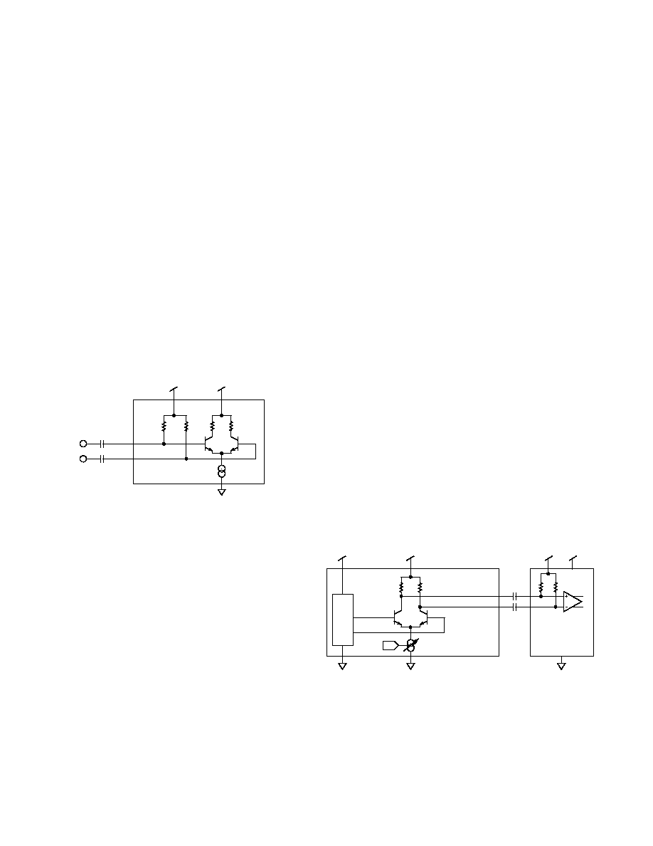
Figure 6. Programming Waveforms
Input/Output Coupling
The AD8152 has internal 50
W termination resistors for each
single-ended input and output. This can also provide a 100
W
termination for a 100
W differential transmission line. All of the
input termination resistors connect to one common point called
VTTI. Similarly, each of the output termination resistors connects
to one common point called VTTO. The voltage can be set
independently at VTTI and VTTO to accommodate various
interface architectures.
REV. A
18
AD8152
Input Coupling
One way to simplify the input circuit and make it compatible with
a wide variety of driving devices is to use ac coupling. This has
the effect of isolating the dc common-mode levels of the driver
and the AD8152 input circuitry. For example, the XAUI inter-
connect specification for 10 Gbps Ethernet requires ac coupling
in order to ensure that there are no interactions of dc levels
between the transmitting and receiving devices.
AC coupling requires that the signal patterns have no long-term
dc component, which may occur in any random data stream.
Codes such as 8b/10b, called for in the XAUI specification, are
used in many data communications systems to ensure that the
data pattern is benign in an ac-coupled link. This is accomplished
by run-length limiting (RLL), which sets a maximum for the
number of 1s or 0s that can occur consecutively. In addition,
residual dc components are monitored and modified by keeping
track of the running disparity, excess of 1s versus 0s or vice versa.
For the AD8152 inputs, ac coupling requires a capacitor in series
with each single-ended input signal, as shown in Figure 7. This
should be done in a manner that does not interfere with the high
speed signal integrity of the PC board. The details of this are
covered in the section on board layout guidelines. The two critical
variables are setting the proper voltage for VTTI and selecting
the correct value of coupling capacitors.
50
VTTI
VCC
50
VEE
INXXP
INXXN
C
INP
C
INN
Figure 7. AC-Coupling Input Signal from AD8152
On the AD8152 side of the input coupling capacitor, the average
value of the single-ended input voltage will be at the voltage set at
VTTI. The range of allowable voltages is a function of the accept-
able input voltages of the active circuitry of the AD8152 inputs
and the amplitude of the input signal. The operating input range
of the AD8152 extends from VCC + 0.2 V to 0.8 V above VEE.
The total range that will be occupied by the input signal will be
its average value (as established by the voltage applied to VTTI)
plus or minus one half the single-ended swing of the signal. For a
standard 800 mV p-p differential signal, the single-ended swing is
400 mV p-p. Thus, the signal will swing
±200 mV about the
average value equal to VTTI.
If VTTI is set equal to VCC, then the single-ended signal will
just meet the specifications where its highest excursion will be
0.2 V higher than VCC. The lowest level to set VTTI is 0.8 V
above VEE. This will cause the negative signal excursions to stay
within the operating range.
With ac-coupled inputs, there is no power consumption advan-
tage associated with varying VTTI. As a practical matter, it
might be desirable to set VTTI at the same voltage as VTTO so
that only one supply is necessary. Refer to the VTTO section for
more information.
Output Coupling
Each single-ended output of the AD8152 has a termination
resistor that ties to a common point called VTTO. When VTTO
is varied, it will change the common-mode levels of the outputs
and the power dissipation of the output stages when they are
enabled.
The individual output currents are programmable. Varying this
current will change the lower level of the output voltage (and thus
the peak-to-peak swing) and also change the power dissipation in
the output stages. To obtain a standard 800 mV p-p differential
output (single-ended = 400 mV p-p), the output current should
be programmed to 16 mA. With an effective termination resis-
tance of 25
W, this will generate the proper differential voltage.
If the AD8152 drives another device that is ac-coupled, there is no
interaction of the dc levels on each side of the coupling capacitors
(see Figure 8). The dc levels for the AD8152 can be calculated
independent of the levels of the device that is driven.
The upper allowable setting for VTTO is 0.2 V higher than VCC.
The signals will be pulled up to this level at their highest excursion.
However at this setting, the power dissipation will be a maximum.
To save power, VTTO can be lowered. The lowest level for
VTTO will be determined by the lowest output level allowable
(V
OL
) by the AD8152 output when it is logically low. The output
at any time should not go lower than 1.0 V below VCC. If the
single-ended swing of an output is 400 mV p-p, then the lowest
that VTTO can go is 0.6 V below VCC. For more information
on V
OL
, see TPC 17.
VTTO
VEE
I = 2mA (CODE) + 2mA
50
50
OUTXXP
OUTXXN
AD8152
VEE
VCC
VTT
VCC
DRIVEN DEVICE
VEE
Figure 8. AC-Coupling Output Signal from AD8152
REV. A
AD8152
19
is powered down. Thus, the total number of active inputs will
affect the total power consumption.
The core of the device performs the crosspoint switching function.
It draws a fixed quiescent current whenever the AD8152 is
powered from VCC to VEE.
An output predriver section draws a current that is proportional
to the programmed output current, I
OUT
. This current always
flows from VCC to VEE. It is treated separately from the output
current, which flows from VTTO, and might not be the same
voltage as VCC.
The final section is the outputs. For an individual output, the
programmed output current will flow through two separate paths.
One is the on-chip termination resistor, and the other is the
transmission line and the destination termination resistor. The
nominal parallel impedance of these two paths is 25
W. The sum
INPUT
TERMINATIONS
INPUTS
OUT-
PUTS
VTTI
VEE
VCC
VTTO
VTT
50
50
INP
INN
50
50
I
OUT
OUTP
OUTN
50
50
OUTPUT TERMINATIONS
V
OL
= V
TTO
(I
OUT
25 )
DRIVEN DEVICE
TERMINATIONS
OPTIONAL COUPLING CAPACITORS
SWITCH
MATRIX
OUTPUT
PRE-
DRIVER
I = 32mA
I = .25 I
OUT
50
I
OUT
2
P =
P =
(V
indiffrms
)
2
100
(V
OL
) (I
OUT
)
P =
I = 2mA
PER
ACTIVE
INPUT
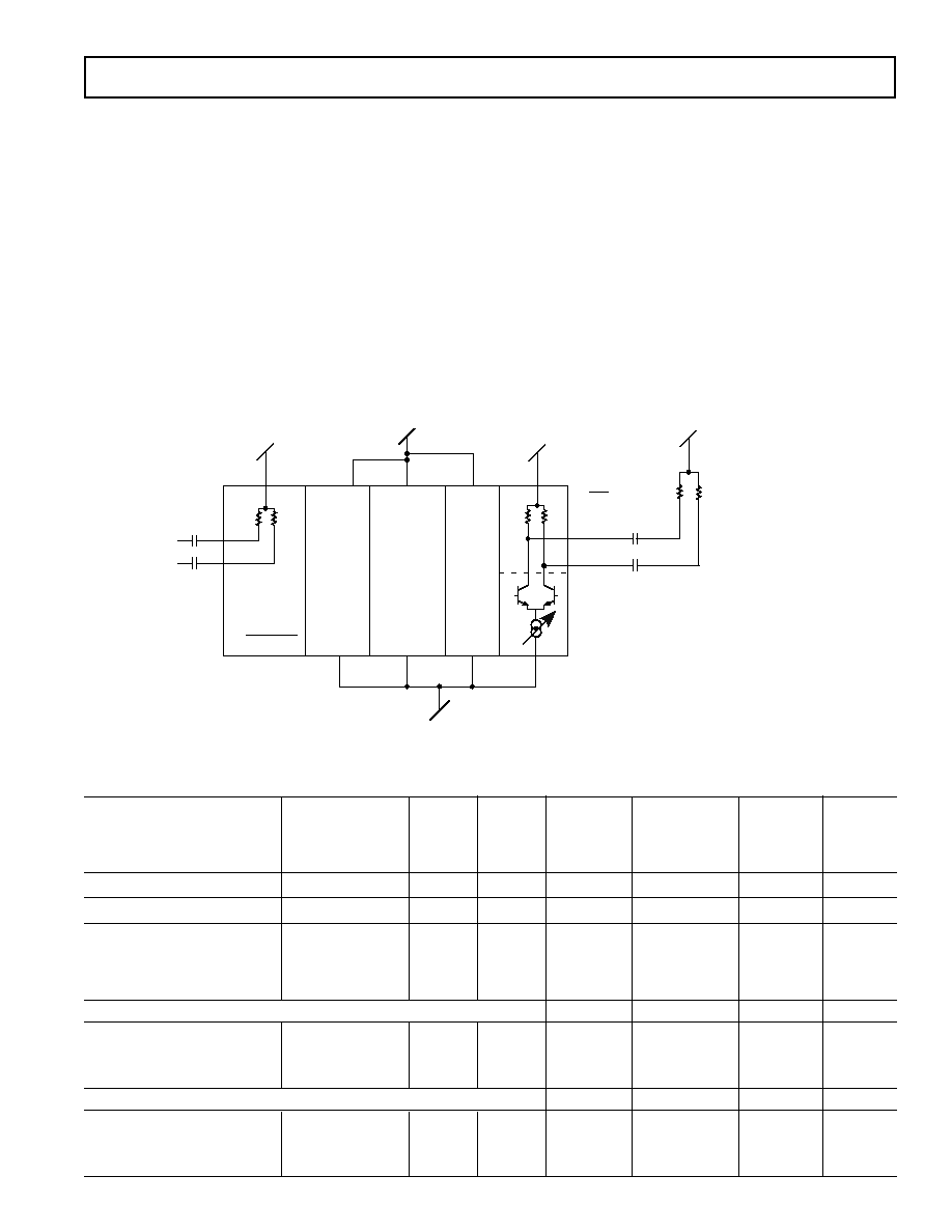
Figure 9. Power Consumption Block Diagram
Table X. Power Consumption
Output
Input
Output
Switch +
Termination
Input
Output
Termination
Current
Total
Resistors
Stage
Core
Predriver
Resistors
Source
Power
Quiescent Current
32 mA
Current per Active Channel
V
IN
/(R
TERMINATION
) 2 mA
0.25
¥ I
OUT
0.5
¥ I
OUT
I
OUT
Current per Active Channel
for Differential
V
IN
= 800 mV p-p Sine
566 mV rms/100
V
OUT
= 800 mV p-p
= 5.66 mA
2 mA
4 mA
4 mA
8 mA
16 mA
2.5 V Operation (VCC VEE = 2.5 V, VTTO = 2.5 V, I
OUT
= 16 mA)
Per Channel Power
3.2 mW
5 mW
10 mW
8 mW
33.6 mW
Power for All Channels Active
108.8 mW
170 mW
80 mW
340 mW
272 mW
1.03 W
2.0 W
Percentage of Total Power
5%
8%
4%
17%
13.6%
51%
3.3 V Operation (VCC VEE = 3.3 V, VTTO = 3.3 V, I
OUT
= 16 mA)
Per Channel Power
3.2 mW
6.6 mW
13.2 mW
8 mW
46.4 mW
Power for All Channels Active
108.8 mW
224 mW
106 mW
449 mW
272 mW
1.47 W
2.63 W
Percentage of Total Power
4%
9%
4%
17%
10%
56%
AD8152 POWER CONSUMPTION
There are several sections of the AD8152 that draw varying
power depending on the supply voltages, the type of I/O coupling
used, and the status of the AD8152 operation. Figure 9 shows a
block diagram of these sections. These are described briefly below
and then in detail later in the data sheet. Table X summarizes the
power consumption of each section and is a useful guide as the
following sections are reviewed.
The first section is the input termination resistors. The power
dissipated in the termination resistors is the result of their being
driven by the respective driving stage. Also, there might be dc power
dissipated in the input termination resistors if the inputs are
dc-coupled and the driving source reference is a dc voltage that is
not equal to VTTI.
In the next section, the active part of the input stages, each input
is powered only when it is selected. If an input is not selected, it

REV. A
20
AD8152
of these two currents will flow through the switches and the current
source of the AD8152 output circuit and out through VEE.
The power dissipated in the transmission line and the destination
resistor will not be dissipated in the AD8152, but will have to be
supplied from the power supply, and is a factor in the overall system
power. The current in the on-chip termination resistors and the
output current source will dissipate power in the AD8152 itself.
Input Termination Resistors
The power dissipated in the input termination resistors is
delivered by the driving source. First, assume the driving wave-
form for an individual input is a differential square wave with an
amplitude of Vinpp. Then the power dissipated in this input is
(Vinpp)
2
/2Rterm.
However, this result is quite pessimistic, because at high fre-
quencies, the wave shape is usually more sinusoidal than square.
If instead, a differential sine wave of amplitude Vinpp is assumed,
then its rms amplitude is 0.7 times that of a square wave. This will
yield a power that is one half of the square wave case. The assumed
wave shape is not too critical because the fraction of the power
dissipated in the input termination resistors is not very large.
A further effect is that the input signal might travel over a path
that attenuates the signal. This will usually be a function of
frequency. Thus, for such a case, some of the signal power will
be dissipated in the signal path. This will reduce the amount of
power dissipated in the AD8152 input terminations.
If dc coupling is used, a dc current will flow from VTTI
through
the termination resistors if the dc voltage of the drive circuit is not
equal to VTTI. The additional power in each input termination
resistor will be the current that flows multiplied by the 50
W
value of the input terminations.
For a point of reference, assume a channel has a sinusoidal input of
800 mV p-p differential. The power dissipated for a single input
will be 3.2 mW. If all 34 input channels are driven the same, then
the power in the input terminations will be 109 mW.
Input Stage
The input stages are powered down when not in use. There is
about 2 mA that flows through an enabled input from VCC to VEE.
Thus, the power dissipated by an enabled input is 5 mW for a
supply of 2.5 V and 6.6 mW for a 3.3 V supply. For all 34 inputs
enabled, the respective figures are 170 mW for a 2.5 V supply
and 224 mW for a 3.3 V supply.
Switch Matrix
The switch matrix draws a fixed 32 mA when the AD8152 is
powered. This current flows from VCC to VEE. The power dissi-
pation from this current is 80 mW at 2.5 V and 106 mW at 3.3 V.
Output Predrivers
The output predrivers draw additional current when each of the
outputs is enabled. This extra current is proportional to the
programmed output current. The extra predriver current for a
channel will be 25 percent of the programmed output current
for that channel. This current will also flow from VCC to VEE.
When an output is enabled and programmed to 16 mA, an addi-
tional 4 mA will flow in the predriver section. This will dissipate
10 mW at 2.5 V or 13.2 mW at 3.3 V for an individual output.
For all 34 outputs enabled and programmed to 16 mA, the
predriver power will be 340 mW at 2.5 V or 449 mW at 3.3 V.
OUTPUTS
The output current is forced by a current source that is pro-
grammed to a variable amount of current from 2 mA to 32 mA
in 2 mA steps. For the two logic switch states, this current flows
through an on-chip termination resistor and a parallel path to the
destination device and its termination resistor. The power in this
parallel path is not dissipated by the AD8152.
The nominal programmed output current is 16 mA. With the two
parallel 50
W resistors at each collector (25 W equivalent), this
current will create a 400 mV p-p swing in each half of the circuit.
The differential output voltage will be 800 mV p-p.
Under steady state conditions and with a data pattern that is
run-length limited so that its low frequency content is significantly
higher than the RC pole formed by the coupling capacitor and the
termination resistors, the common-mode level at the AD8152
outputs will be 400 mV lower than VTTO. Each output will then
swing
±200 mV from this level, which is a 400 mV p-p single-
ended output swing.
At the high level, there will be 200 mV across the termination
resistor. This will dissipate a power of 0.8 mW. At the low level, the
600 mV across the termination resistor will dissipate a power of
7.2 mW. Since the output signal is basically 50% duty cycle, the
average power dissipated will be the average of these two values
or 4 mW. By symmetry, the other differential output will dissipate
the same power. This yields an on-chip termination-resistor
power dissipation of 8 mW per channel for each output, or 272 mW
for all 34 outputs.
The full output current (from both on- and off-chip termination
resistors) will flow in the lower part of each output. This current
flows only in the side that is "on," or in its low state (V
OL
). This
voltage is 600 mV below the dc level at VTTO.
Thus, for VTTO = 2.5 V, V
OL
= 1.9 V, and the power dissipa-
tion for I
OUT
= 16 mA is 30.4 mA. For all 34 channels, the
power is 1.03 W.
If VTTO = 3.3 V, then V
OL
= 2.7 V. The single power is 43.2 mW
and the power for all 34 channels is 1.47 W.
If VTTO = 2.5 V, then the additional power is given by 16 mA
¥ [(2.5 V (16 mA ¥ 25 W)] = 33.6 mW. Thus, the total AD8152
power dissipation for this output is 37.6 mW.
If all 34 outputs are enabled with the same I
OUT
, the total power
dissipation is 1.28 W. Thus it can be seen that the outputs are
the major contributor to the power dissipation.
Power Saving Considerations
While the AD8152 power consumption is very low compared to
similar devices, careful control of its operating conditions can yield
further power savings. Significant power reduction can be realized
by operating the part at a lower voltage. Compared to 3.3 V
operation, a supply voltage of 2.5 V can result in power savings of
about 25 percent. There is virtually no performance penalty when
operating at lower voltage.
A second measure is to disable outputs when they are not being
used. This can be done on a static basis if the output is not used,
or on a dynamic basis if the output does not have a constant
stream of traffic.
Since the majority of the power dissipated is in the output stage,
some of its flexibility can be used to lower the power consumption.
REV. A
AD8152
21
First, the output current can be programmed to the smallest amount
required to maintain BER performance. If an output circuit
always has a short length and the receiver has good sensitivity,
then a lower output current can be used.
It is also possible to lower the voltage on VTTO to lower the
power dissipation. The amount that VTTO can be lowered is
dependent on the lowest of all the output's V
OL
. This will be
determined by the output that is operating at the highest pro-
grammed output current since V
OL
= VTTO (I
OUT
¥ 25 W).
EVALUATION BOARD AND PCB LAYOUT HINTS
The AD8152 evaluation board was designed to allow the user to
analyze signal integrity in many configurations, as controlled by
a standard PC.
The FR4 board comes equipped with a full complement of
136 SMA connectors to support the complete 34 34 matrix of
points. Each differential pair of microstrip is connected to either
top mount or side-launch SMA connectors. The mounting area of
the short center pin top-mount SMA connectors are drilled (seven
holes) and stubbed for greatly improved performance. In the
area surrounding SMA top-mount center pin and drill holes, all
internal planes are relieved or cleared out (see Figure 10 for layout).
ALL TOP-MOUNT SMAs SIT ON PCB TOP LEVEL
TOP VIEW OF TOP LEVEL TRACE
MICROSTRIP
SMA CENTER PIN
PLANE RELIEF
DRILL HOLES
(7 EACH)
BOTTOM VIEW OF BOTTOM LEVEL TRACE
Figure 10. Top-Mount SMA PCB Layout, Two Views
The FR4 PC board is eight layers with a thickness of 62 mils
(1.57 mm). The two outer most metal layers hold the high speed
microstrip routing lines. The two outer most dielectric layers are
5 mils thick and must be controlled impedance (50
W) layers. These
are the only two layers that require controlled impedance. The
next two inner metal layers are ground (reference) planes for the
microstrip and are the shell for the SMA connectors. The remain-
ing four inner metal layers are for the four AD8152 supply and
digital control signal routing. From top to bottom the four supply
layers are VTTO, VCC, VEE, and VTTI. Because all four supply
PCB metal layers float, positive, negative, and even dual-supply
configurations are possible. The variety of supply configurations
ease the connection of test equipment. The four inner supply
layers also provide an interlayer capacitance, which has better
impedance versus frequency than standard chip capacitors.
DIELECTRIC
THICKNESS
SILKSCREEN
COPPER
LAYER
NUMBER
1. 1.50/
TOP
MICROSTRIP
WIDTH
=
8.0mils
2. 0.50/GND
3. 0.50/VTTO
4. 0.50/VCC
5.
0.50/VEE
6.
0.50/VTTI
7.
0.50/GND
8.
1.50/BOTTOM MICROSTRIP WIDTH = 8.0mils
0.5mils
5.0mils
4.0mils
16.0mils
4.0mils
16.0mils
4.0mils
5.0mils
0.5mils
SILKSCREEN
THICKNESS/DESIGNATION
(IN OUNCES)
Figure 11. Evaluation Board Stack-Up
REV. A
22
AD8152
The variety of supply configurations cause the need for a supply
agile digital control circuitry. This is done by a programmable
logic device (PLD), which provides instructions to the AD8152.
The PLD supply is typically tied with jumpers across the AD8152's
VCC and VEE supplies (Jumpers J3 and J4). The PLD is addressed
from the PC by way of digital isolators. These couplers isolate
PC levels from the PLD and allow for any level shifting. If
desired, the user can drive the PLD supply separately as long as
the VEE of the AD8152 and the PLD are tied together (remove
Jumper J3 and leave J4 installed). This allows one to measure
the AD8152 only supply current, for example.
Board Construction or Stack-Up
Figure 11 is a picture of AD8152 evaluation board stack-up from
top to bottom. The layer stack-up has been made symmetrical
to avoid board warpage during manufacture. The microstrip
layout and dimensions are shown in Figure 12. The microstrip
trace width was chosen to be 8 mils. This allows relative ease in
routing through the BGA rows that are 50 mils (1.27 mm) apart.
The outer two out of four rows of high speed signals are routed on
top of the PCB, while the inner two rows are via holed to the
board's opposite side and then routed outward. Wider microstrip
is desirable for reducing eye height loss versus long traces; how-
ever, the routing will be more difficult as the AD8152 is approached.
The wide microstrip would have to be necked down in width in
order to be routed into the BGA. The necking will increase trace
impedance and therefore induce more signal reflection problems.
MICROSTRIP TRACES
BGA CORNER OUTLINE
VIA HOLE
(GRAY)
CHIP CAPACITOR
(805) SIZE
Figure 13. BGA Corner Capacitor Layout
Figure 12. Cross-Sectional Layout and Dimensioning (To Scale) of Differential
During the layout of the differential microstrip, a software tool
snaps the distance between the two traces to be a constant. If
the distance is not kept constant, impedance variations will
result. These fluctuations can be measured by time domain
reflectometry (TDR).
EXTRA ADDED INDUCTANCE
Figure 14. Poor Capacitor Layout
Bypass Capacitor Layout
The AD8152 8-layer PCB takes advantage of buried interlayer
capacitance. The VEE to VCC planes are placed in the very middle
of the board to make the highest value capacitor. The 4 mil
(0.102 mm) dielectric spacing between VCC/VEE yields 26 nF
of capacitance. Each AD8152 supply pin is directly connected to
its supply plane through a via hole beneath the BGA ball. The
via hole size for a BGA supply pin is slightly bigger than a signal
via. This is to reduce the inductance of the connection, and it
also happens to be a compact layout.
For the chip capacitors, the via holes are placed directly in the
middle of the mounting area and made as large as possible, i.e.,
greater than or equal to 35 mils (0.89 mm). This is to minimize
inductance as much as possible. By minimizing inductance, the
performance of the capacitor or impedance versus frequency
response is not greatly diminished. Note that chip capacitors
will work up to only about 300 MHz.
Figure 14 is an example of a bypass capacitor layout that should
be avoided in any high speed printed circuit board. This layout
connects the chip capacitor mounting pads to small via holes
through a skinny PCB trace. This amounts to four extra inductors
added to the capacitor, two largely from the skinny surface traces
and two from small via holes. Inductance is also variable with
copper thickness and attachment method to power plane. Thermal
relief for soldering purposes also adds unwanted inductance and
should be avoided.
REV. A
AD8152
23
ECL
DRIVER
TO 50
SCOPE
INPUTS
VCC
VTTO
VTTI
= 2V
VEE
= 2.5V
AD8152
P
P
N
N
IN
OUT
Figure 15. Evaluation Board ECL Driver Test Setup
Connections for Testing
The AD8152 evaluation board can be used under a variety of posi-
tive or negative supply configurations. Negative supply configurations,
as shown in Figure 15, allow the easiest hookup to test equip-
ment because inputs and outputs can be direct coupled. In a real
world application however, the negative supply configuration would
be difficult because control logic levels must be shifted negative.
Figure 16 is an example of a loop-through test setup using a posi-
tive supply. In this case, the test signal goes through the AD8152
twice. It is possible to loop through multiple times if desired, but
jitter will increase with number of loop-throughs. The first
input from the generator and the last output to a scope must be
ac-coupled. However, an AD8152 output driving its own input can
be direct-coupled. Direct coupling to the first AD8152 input is not
effective since generators usually want to see 50
W to ground.
This would require VTTI to be attached to ground, causing
excessive power to be dissipated in the internal 50
W input
termination resistors. Secondly, when the AD8152 output tries
to drive its own input with VTTI = 0 V and VTTO = 2.5 V, the
input will pull the output stage levels down enough to shut off
any signal toggling.
All ac coupling shown is actually done with a set of bias tees. If
desired, the bias tee can be used to monitor average dc voltage
levels at an input or output (depending on direction installed),
and it can also serve to change input dc levels. Make sure the
bias tees used in the setup have enough low frequency bandwidth
to pass long patterns and keep edge rates intact. The longer the
pattern, the more low frequency bandwidth is needed.
If ac coupling is desired on a user board, 0402 or 0603 sized
capacitors can be installed on microstrip lines. The biggest 0402
size, XR7 type usable is 0.01
mF, which will work fine for short
patterns (PRBS 2
7
1) and data rates down to 1.0 Gbps. For
long patterns a 0603 sized, XR7 type, 0.1
mF should be used. To
decrease capacitive loading from the mounting area, clear out
planes underneath the coupling capacitor.
In Figure 16, 6 dB attenuators are placed before the AD8152
input ac-coupling or bias tees. This is because many generators
won't go below 500 mV single-ended. The output pair of 6 dB
attenuators is present to protect the scope inputs and allow for
higher scale voltages per division. The eye diagram is usually
viewed differentially by using a simple P N math function.
Cabling used in this setup must be matched. Mismatched cables
cause either a P or N signal to be falsely delayed. This delay can
show up as a change in the crossing point, from 50 percent in the
eye diagram. To accurately check cable matches, a TDR setup
is recommended.
PATTERN
GENERATOR
VCC
VTTO
2.5V
AD8152
P
P
N
N
IN01
OUT01
VTTI
P
N
P
N
IN02
OUT02
VEE
50
50
DATA OUT
DATA OUT
TRIGGER OUT
TRIGGER IN
HIGH SPEED
SAMPLING
OSCILLOSCOPE
6dB
6dB
6dB
6dB
VCC = VTTI = VTTO = 2.5V, VEE = 0V, I
OUT
SET = 16mA
RTI (REFERRED TO INPUT) A MPLITUDE = 400mV SINGLEENDED,
V
IN
HI = 2.7V (IN01), PRBS 2
23
1, V
OH
= 2.5V,
V
OL
= 2.1V,
AC-COUPLED IS FROM BIAS TEES,
PROGRAMMING: IN01 TO OUT02, IN02 TO OUT01.
Figure 16. Positive Supply Loop-Through Test Setup
REV. A
24
AD8152
EVALUATION BOARD CONTROL SOFTWARE
The AD8152 evaluation board can be controlled by using a PC
and a custom software program. The hardware interface uses a
PC parallel (or printer) port. A standard printer cable is used to
connect from the PC DB-25 connector to the Centronics-type
connector on the evaluation board. Figure 17 shows an evaluation
board control panel from a PC display.
A single screen allows control of all the programmable functions
of the AD8152. The programming modes are listed in the Mode
box. Select either I/O Programming or Current Programming by
selecting the appropriate radio button. These will allow either
programming the switch matrix or the output currents one at a time.
An alternative is to use the Broadcast mode. This will either
simultaneously program all of the outputs to one selected input
or program all outputs to the same current.
Figure 17. Evaluation Board Control Panel
In the I/O Programming mode (nonbroadcast), the desired input
is selected from the Input Select box by double-clicking on the
appropriate input channel number. This will cause the same
channel to appear in the Active Input Selection indicator window.
Next, select the desired output from the Output Select box by double-
clicking the appropriate output channel number.
Finally, the Program button is clicked and the data is immediately
sent to the evaluation board for programming the part to the
selected I/O combination.
If an additional output(s) is desired to be programmed to the same
input, double-click the desired output channel number and click
the Program button.
The Programmed Output table indicates which outputs are
programmed to the input that is indicated in the Active Input
Selection window. If it is desired to disable an individual output,
its radio button in the Programmed Output table can be clicked,
and it will change from black to white to indicate that it is not
enabled. Note: It is not possible to program outputs by selecting
their radio buttons.
To observe the set of outputs that are connected to any input,
double-click the desired input channel number from the Input
Select box. The selected channel number will show up in the Active
Input Selection window and the programmed outputs will have a
black dot in their radio button in the Programmed Output table.
To program an output current, select the Current Programming
button in the Mode box. Then double-click the desired output
channel number from the Output Select table. Next double-click
the desired entry for the Output Current. Finally, click the
Program button.
If the Broadcast button is selected from the Mode box, all outputs
will be treated the same. If I/O Programming is selected, double-
click the input channel number from the Input Select table
and click the Program button. This will cause all outputs to be
programmed to the selected output, and all of the buttons will
have a black dot in the Programmed Output table.
For broadcast current programming, double-click the desired
Output Current. Then click the Program button. All of the outputs
will be programmed to the selected output current.
The Reset button will disable all outputs. In addition, all output
currents will be programmed to the nominal value of 16 mA.
REV. A
AD8152
25
Figure 18. Evaluation Board Top Side Signals
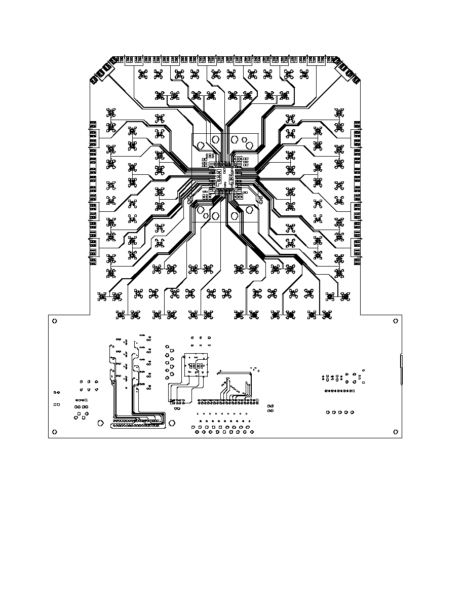
REV. A
26
AD8152
Figure 19. Evaluation Board Bottom Side Signals, View from Top
REV. A
AD8152
27
Figure 20. Evaluation Board VCC Layer, View from Top
REV. A
28
AD8152
Figure 21. Evaluation Board VEE Layer, View from Top
REV. A
AD8152
29
Figure 22. Evaluation Board VTTI Layer, View from Top
REV. A
30
AD8152
Figure 23. Evaluation Board VTTO Layer, View from Top
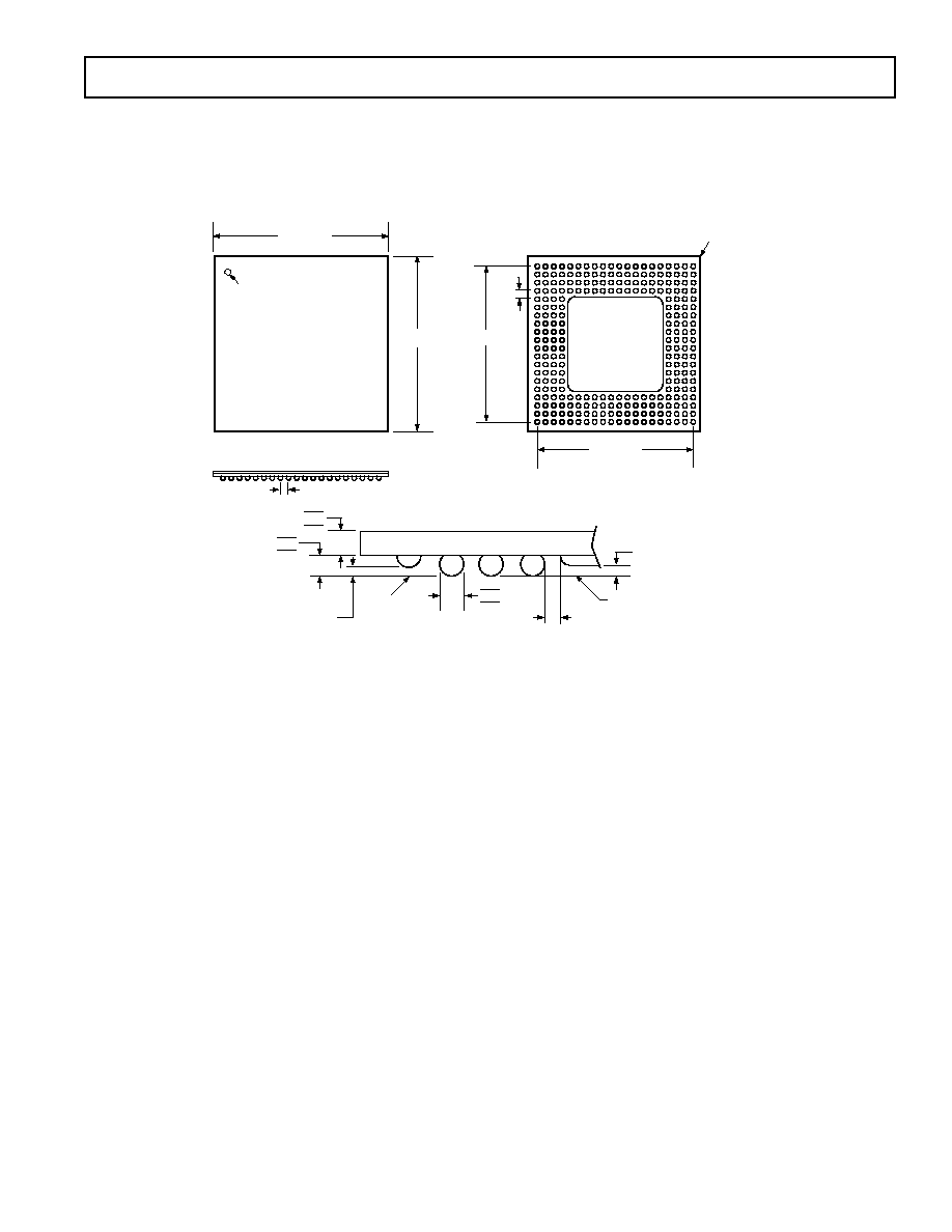
REV. A
AD8152
31
OUTLINE DIMENSIONS
256-Ball Grid Array [SBGA]
(BP-256)
Dimensions shown in millimeters
A
B
C
D
E
F
G
H
J
K
L
M
N
P
R
T
U
V
W
Y
1
3
5
7
9
11
13
15
17
19
2
4
6
8
10
12
14
16
18
20
A1 CORNER
27.00 BSC
24.13 REF
1.27
BOTTOM
0.20 MIN
SEATING PLANE
0.25 MIN
0.90
0.75
0.60
TOP
1.27
0.70
0.60
0.50
1.00
0.80
0.60
0.20
COPLANARITY
SEATING
PLANE
BALL DIAMETER
24.13 REF
27.00 BSC
A1
COMPLIANT TO JEDEC STANDARDS MO-192-BAL-2

C0298401/03(A)
PRINTED IN U.S.A.
32
REV. A
AD8152
Revision History
Location
Page
1/03--Data Sheet changed from REV. 0 to REV. A.
Edits to SPECIFICATIONS . . . . . . . . . . . . . . . . . . . . . . . . . . . . . . . . . . . . . . . . . . . . . . . . . . . . . . . . . . . . . . . . . . . . . . . . . . . . . . . 2
Document Outline
- FEATURES
- APPLICATIONS
- GENERAL DESCRIPTION
- FUNCTIONAL BLOCK DIAGRAM
- ELECTRICAL CHARACTERISTICS
- ABSOLUTE MAXIMUM RATINGS
- MAXIMUM POWER DISSIPATION
- ORDERING GUIDE
- BALL GRID ARRAY
- BALL GRID DESCRIPTIONS
- Typical Performance Characteristics
- CONTROL INTERFACE
- CONTROL PIN DESCRIPTION
- A[6:0] Inputs
- D[5:0] Inputs/Outputs
- WE Input
- UPDATE Input
- RE Input
- CS Input
- RESET Input
- Control Interface Levels
- Output Addressing
- Using the Data Bus
- Output-Current Programming
- Register-Control Signals
- Input/Output Coupling
- Input Coupling
- Output Coupling
- AD8152 POWER CONSUMPTION
- Input Termination Resistors
- Input Stage
- Switch Matrix
- Output Predrivers
- OUTPUTS
- Power Saving Considerations
- EVALUATION BOARD AND PCB LAYOUT HINTS
- Board Construction or Stack-Up
- Bypass Capacitor Layout
- Connections for Testing
- EVALUATION BOARD CONTROL SOFTWARE
- OUTLINE DIMENSIONS
- Revision History