 | ÐлекÑÑоннÑй компоненÑ: AD816 | СкаÑаÑÑ:  PDF PDF  ZIP ZIP |
Äîêóìåíòàöèÿ è îïèñàíèÿ www.docs.chipfind.ru
REV. B
Information furnished by Analog Devices is believed to be accurate and
reliable. However, no responsibility is assumed by Analog Devices for its
use, nor for any infringements of patents or other rights of third parties
which may result from its use. No license is granted by implication or
otherwise under any patent or patent rights of Analog Devices.
a
500 mA Differential Driver and
Dual Low Noise (VF) Amplifiers
AD816*
FEATURES
Flexible Configuration
Two Low Noise Voltage Feedback Amplifiers with
High Current Drive, Ideal for ADSL Receivers or
Drivers for Low Impedance Loads such as CRT Coils
Two High Current Drive Amplifiers, Ideal for an ADSL
Differential Driver or Single Ended Drivers for Low
Impedance Loads such as CRT Coils
Thermal Overload Protection
CURRENT FEEDBACK AMPLIFIERS/DRIVERS
High Output Drive
26 dBm Differential Line Drive for ADSL Transmitters
40 V p-p Differential Output Voltage, R
L
= 50
@ 1 MHz
500 mA Continuous Current, R
L
= 5
1 A Peak Current, 1% Duty Cycle, R
L
= 15
for DMT
Low Distortion
68 dB @ 1 MHz THD, R
L
= 100 , V
O
= 40 V p-p
High Speed
120 MHz Bandwidth (3 dB)
1500 V/ s Differential Slew Rate, V
O
= 10 V p-p, G = +5
70 ns Settling Time to 0.1%
VOLTAGE FEEDBACK AMPLIFIERS/RECEIVERS
High Input Performance
4 nV/
Hz Voltage Noise
15 mV Max Input Offset Voltage
Low Distortion
68 dB @ 1 MHz THD, V
O
= 10 V p-p, R
L
= 200
High Speed
100 MHz Bandwidth (3 dB)
180 V/ s Slew Rate
High Output Drive
70 mA Output Current Drive
APPLICATIONS
ADSL, VDSL and HDSL Line Interface Driver and Receiver
CRT Convergence and Astigmatism Adjustment
Coil and Transformer Drivers
Composite Audio Amplifiers
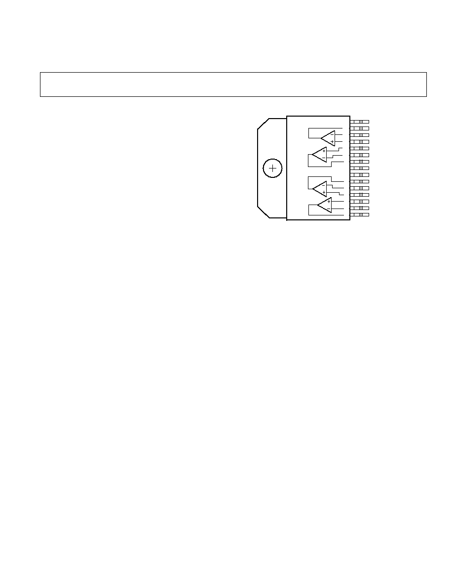
FUNCTIONAL BLOCK DIAGRAM
OUT1 RECEIVER
IN1 RECEIVER
+IN1 RECEIVER
+IN1 DRIVER
IN1 DRIVER
OUT1 DRIVER
V
S
+V
S
OUT2 RECEIVER
IN2 DRIVER
+IN2 DRIVER
+IN2 RECEIVER
IN2 RECEIVER
NC
TAB IS
+V
S
NC = NO CONNECT
OUT2 DRIVER
RECEIVER A
RECEIVER B
AD816
V
S
+V
S
DRIVER A & B
B
A
15
14
13
12
11
10
9
8
7
6
5
4
3
2
1
PRODUCT DESCRIPTION
The AD816 consists of two high current drive and two low
noise amplifiers. These can be configured differentially for driv-
ing low impedance loads and receiving signals over twisted pair
cable or could be used independently for single ended driving
application such as correction circuits within high resolution
CRT Monitors.
The two high output drive amplifiers are capable of supplying
a minimum of 500 mA continuous output current and up to
1A peak output current, and when configured differentially,
40 V p-p differential output swing can be achieved on
±
15 V
supplies into a load of 50
. The drivers have 120 MHz of
bandwidth and 1,500 V/
µ
s of differential slew rate while
featuring total harmonic distortion of 68 dB at 1 MHz into a
100
load, specifications required for high frequency telecom-
munication subscriber line drivers.
The low noise voltage feedback amplifiers are fully independent
and can be configured differentially for use as receiver amplifi-
ers within a subscriber line hybrid interface or individually for
signal conditioning or filtering. The low noise of 4 nV/
Hz and
distortion of 68 dB at 1 MHz enable low level signals to be
resolved and amplified in the presence of large common-mode
voltages. 100 MHz of bandwidth and 180 V/
µ
s of slew rate
combined with a load drive capability of 70 mA enable these
amplifiers to drive passive filters and low inductance coils. The
AD816 has thermal overload protection for system reliability
and is available in low thermal resistance power packages. The
AD816 operates over the industrial temperature range (40
°
C
to +85
°
C).
One Technology Way, P.O. Box 9106, Norwood, MA 02062-9106, U.S.A.
Tel: 781/329-4700
World Wide Web Site: http://www.analog.com
Fax: 781/326-8703
© Analog Devices, Inc., 1999

AD816SPECIFICATIONS
DRIVER AMPLIFIERS
AD816A
Model
Conditions
V
S
Min
Typ
Max
Units
DYNAMIC PERFORMANCE
Small Signal Bandwidth (3 dB)
G = +2, R
F
= 499
, V
IN
= 0.125 V rms,
R
L
= 100
±
15
100
120
MHz
G = +2, R
F
= 499
, V
IN
= 0.125 V rms,
R
L
= 100
±
5
90
110
MHz
Bandwidth (0.1 dB)
G = +2, R
F
= 499
, V
IN
= 0.125 V rms,
R
L
= 100
±
15
10
MHz
Differential Slew Rate
V
OUT
= 10 V p-p, G = +5, R
L
= 100
±
15
1400
1500
V/
µ
s
Settling Time to 0.1%
10 V Step, G = +2
±
15
70
ns
NOISE/HARMONIC PERFORMANCE
Total Harmonic Distortion (Differential)
f = 1 MHz, R
LOAD
= 100
, V
OUT
= 40 V p-p
±
15
68
dBc
Input Voltage Noise
f = 10
kHz, G = +2 (Single Ended)
±
5,
±
15
1.85
nV/
Hz
Input Current Noise (+I
IN
)
f = 10 kHz, G = +2
±
5,
±
15
1.8
pA/
Hz
Input Current Noise (I
IN
)
f = 10 kHz, G = +2
±
5,
±
15
19
pA/
Hz
Differential Gain Error
NTSC, G = +2, R
LOAD
= 25
±
15
0.05
%
Differential Phase Error
NTSC, G = +2, R
LOAD
= 25
±
15
0.45
Degrees
DC PERFORMANCE
Input Offset Voltage
±
5
5
12
mV
±
15
10
15
mV
T
MIN
to T
MAX
25
mV
Input Offset Voltage Drift
40
µ
V/
°
C
Differential Offset Voltage
±
5,
±
15
0.5
2
mV
T
MIN
to T
MAX
5
mV
Differential Offset Voltage Drift
5
µ
V/
°
C
Input Bias Current
±
5,
±
15
20
60
µ
A
T
MIN
to T
MAX
100
µ
A
+Input Bias Current
±
5,
±
15
2
5
µ
A
T
MIN
to T
MAX
5
µ
A
Differential Input Bias Current
±
5,
±
15
10
50
µ
A
T
MIN
to T
MAX
50
µ
A
Open-Loop Transresistance
V
OUT
=
±
10 V, R
L
= 1 k
±
5,
±
15
0.7
2
M
T
MIN
to T
MAX
0.6
M
INPUT CHARACTERISTICS
Differential Input Resistance
+Input
±
15
7
M
Input
15
Differential Input Capacitance
±
15
1.4
pF
Input Common-Mode Voltage Range
±
15
13.5
±
V
±
5
3.5
±
V
Common-Mode Rejection Ratio
T
MIN
to T
MAX
±
5,
±
15
56
60
dB
Differential Common-Mode Rejection Ratio
T
MIN
to T
MAX
±
5,
±
15
80
100
dB
OUTPUT CHARACTERISTICS
Voltage Swing
Single Ended, R
LOAD
= 25
±
15
23
24.5
V p-p
±
5
2.2
3.6
V p-p
Differential, R
LOAD
= 50
±
15
46
49
V p-p
T
MIN
to T
MAX
±
15
45
V p-p
Continuous Output Current
R
LOAD
= 5
±
15
500
750
mA
±
5
200
100
mA
Peak Output Current
10
µ
s Pulse, 1% Duty Cycle, R
L
= 15
±
15
1.0
A
Short Circuit Current
Note 1
±
15
1.0
A
NOTES
1
See Power Considerations section.
Specifications subject to change without notice.
REV. B
2
(@ T
A
= +25 C, V
S
= 15 V dc, R
F
= 1 k
and R
LOAD
= 50
unless otherwise noted)

RECEIVER AMPLIFIERS
AD816A
Model
Conditions
V
S
Min
Typ
Max
Units
DYNAMIC PERFORMANCE
Small Signal Bandwidth (3 dB)
G = +2, R
L
= 100
±
15
100
MHz
G = +2, R
L
= 100
±
5
80
MHz
Bandwidth (0.1 dB)
G = +2
±
15
30
MHz
G = +2
±
5
40
MHz
Slew Rate
V
OUT
= 4 V p-p
±
15
180
V/
µ
s
Settling Time to 0.1%
V
OUT
= 10 V p-p Step, G = +2
±
15
45
ns
NOISE/HARMONIC PERFORMANCE
Total Harmonic Distortion
f = 1 MHz, R
LOAD
= 200
±
15
68
dBc
Input Voltage Noise
f = 10
kHz
±
5,
±
15
4
nV/
Hz
Current Noise
f = 10 kHz
±
5,
±
15
2
pA/
Hz
Differential Gain Error
NTSC, G = +2, R
LOAD
= 150
±
15
0.04
0.08
%
±
5
0.05
0.1
%
Differential Phase Error
NTSC, G = +2, R
LOAD
= 150
±
15
0.03
0.1
Degrees
±
5
0.06
0.1
Degrees
DC PERFORMANCE
Input Offset Voltage
±
5,
±
15
7.5
15
mV
T
MIN
to T
MAX
15
mV
Offset Voltage Drift
20
µ
V/
°
C
Input Bias Current
±
5,
±
15
5
7
µ
A
T
MIN
to T
MAX
15
µ
A
Input Offset Current
±
5,
±
15
0.5
2
µ
A
Offset Current Drift
1
nA/
°
C
Open-Loop Gain
V
OUT
=
±
7.5 V, R
LOAD
= 150
±
15
3
6
V/mV
T
MIN
to T
MAX
±
15
1
V/mV
INPUT CHARACTERISTICS
Input Resistance
300
k
Input Capacitance
1.5
pF
Input Common-Mode Voltage Range
±
15
+13
+14.3
V
±
15
12
13.4
V
±
5
+3.8
+4.3
V
±
5
2.7
3.4
V
Common-Mode Rejection Ratio
V
CM
=
±
5 V
±
15
82
110
dB
OUTPUT CHARACTERISTICS
Output Voltage Swing
Single Ended, R
LOAD
= 150
±
15
25.2
25.5
V p-p
T
MIN
to T
MAX
±
15
25.2
V p-p
Single Ended, R
LOAD
= 150
±
5
6.2
6.4
V p-p
T
MIN
to T
MAX
±
5
6.0
V p-p
Output Current
R
L
= 150
±
15
65
70
mA
Short Circuit Current
±
15
105
mA
Specifications subject to change without notice.
(@ T
A
= +25 C, V
S
= 15 V dc, R
F
= 1 k
and R
LOAD
= 500
unless otherwise noted)
REV. B
3
COMMON CHARACTERISTICS
AD816A
Model
Conditions
V
S
Min
Typ
Max
Units
MATCHING CHARACTERISTICS
Crosstalk:
Driver to Driver
f = 1 MHz, V
IN
= 200 mV rms, R
LOAD
= 100
±
15
67
dB
Drivers to Receivers
f = 1 MHz, V
IN
= 200 mV rms, R
LOAD
= 100
±
15
64
dB
Receiver to Receiver
f = 1 MHz, V
IN
= 200 mV rms, R
LOAD
= 500
±
15
81
dB
POWER SUPPLY
Operating Range
±
5
±
18
V
Quiescent Current
±
15
46
56
mA
T
MIN
to T
MAX
±
15
59
mA
Driver Supply Rejection Ratio
T
MIN
to T
MAX
±
15,
±
5
49
66
dB
Receiver Supply Rejection Ratio
T
MIN
to T
MAX
±
15,
±
5
69
75
dB
Specifications subject to change without notice.
(@ T
A
= +25 C, V
S
= 15 V dc, R
F
= 1 k
and R
LOAD
= 50
(Driver), R
LOAD
= 500
(Receiver)
unless otherwise noted)
AD816
AD816
REV. B
4
MAXIMUM POWER DISSIPATION
The maximum power that can be safely dissipated by the
AD816 is limited by the associated rise in junction temperature.
The maximum safe junction temperature for the plastic encap-
sulated parts is determined by the glass transition temperature
of the plastic, about 150
°
C. Exceeding this limit temporarily
may cause a shift in parametric performance due to a change in
the stresses exerted on the die by the package. Exceeding a
junction temperature of 175
°
C for an extended period can result
in device failure.
The AD816 has thermal shutdown protection, which guarantees
that the maximum junction temperature of the die remains below a
safe level. However, shorting the output to ground or either power
supply for an indeterminate period will result in device failure.
To ensure proper operation, it is important to observe the derat-
ing curves and refer to the section on power considerations.
It must also be noted that in high (noninverting) gain configura-
tions (with low values of gain resistor), a high level of input
overdrive can result in a large input error current, which may
result in a significant power dissipation in the input stage. This
power must be included when computing the junction tempera-
ture rise due to total internal power.
AMBIENT TEMPERATURE C
14
7
4
50
90
40
MAXIMUM POWER DISSIPATION Watts
30 20 10
10
20 30
40
50 60
70 80
13
8
6
5
11
9
12
10
0
T
J
= 150 C
3
2
1
0
AD816 AVR, AY
JA
= 41 C/W
(STILL AIR = 0FT/MIN)
NO HEAT SINK
JA
= 16 C/W
SOLDERED DOWN TO
COPPER HEAT SINK AREA
(STILL AIR = 0FT/MIN)
AD816 AVR, AY
Figure 1. Plot of Maximum Power Dissipation vs. Tem-
perature (Copper Heat Sink Area = 2 in.
2
)
ABSOLUTE MAXIMUM RATINGS
1
Supply Voltage . . . . . . . . . . . . . . . . . . . . . . . . . . .
±
18 V Total
Internal Power Dissipation
2
Plastic (Y, YS and VR) . . 3.05 W (Observe Derating Curves)
Input Voltage (Common Mode) . . . . . . . . . . . . . . . . . . . .
±
V
S
Differential Input Voltage . . . . . . . . . . . . . . . . . . . . . . . .
±
6 V
Output Short Circuit Duration
. . . . . . . . . . . . . . . . . . . . . . Observe Power Derating Curves
Storage Temperature Range
Y, YS, VR Package . . . . . . . . . . . . . . . . . . 65
°
C to +125
°
C
Operating Temperature Range
AD816A . . . . . . . . . . . . . . . . . . . . . . . . . . . 40
°
C to +85
°
C
Lead Temperature Range (Soldering, 10 sec) . . . . . . . +300
°
C
NOTES
1
Stresses above those listed under Absolute Maximum Ratings may cause perma-
nent damage to the device. This is a stress rating only. functional operation of the
device at these or any other conditions above those indicated in the operational
section of this specification is not implied. Exposure to absolute maximum rating
conditions for extended periods may affect device reliability.
2
Specification is for device in free air: 15-Lead Through Hole and Surface Mount:
JA
= 41
°
C/W.
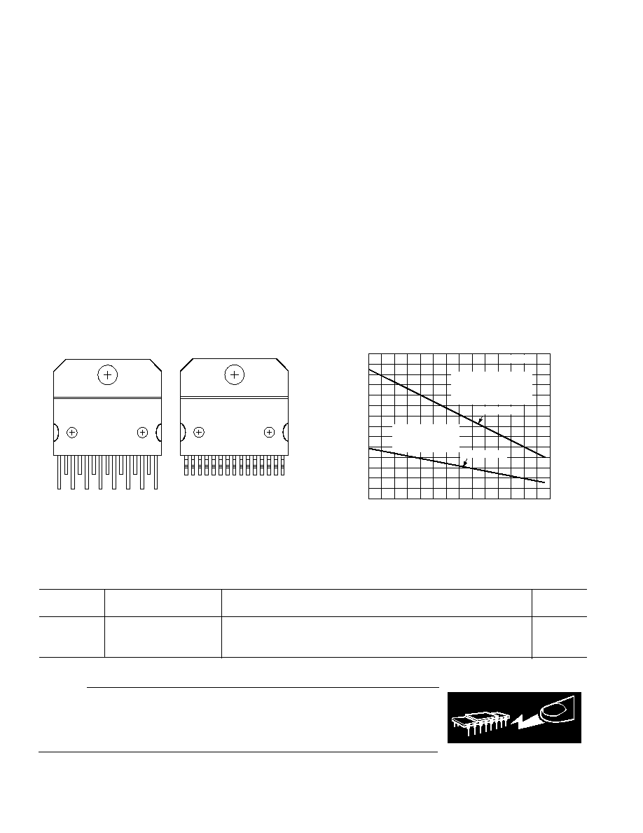
PIN CONFIGURATION
Y-15 VR-15, YS-15
TOP VIEW
10
12
13
14
15
11
1
2
3
4
5
6
7
8
9
OUT1 RECEIVER
IN1 RECEIVER
+IN1 RECEIVER
+IN1 DRIVER
IN1 DRIVER
OUT1 DRIVER
V
S
+V
S
OUT2 RECEIVER
IN2 DRIVER
+IN2 DRIVER
+IN2 RECEIVER
IN2 RECEIVER
NC
OUT2 DRIVER
OUT1 RECEIVER
IN1 RECEIVER
+IN1 RECEIVER
+IN1 DRIVER
IN1 DRIVER
OUT1 DRIVER
V
S
+V
S
OUT2 RECEIVER
IN2 DRIVER
+IN2 DRIVER
+IN2 RECEIVER
IN2 RECEIVER
NC
OUT2 DRIVER
TOP VIEW
10
12
13
14
15
11
1
2
3
4
5
6
7
8
9
CAUTION
ESD (electrostatic discharge) sensitive device. Electrostatic charges as high as 4000 V readily
accumulate on the human body and test equipment and can discharge without detection.
Although the AD816 features proprietary ESD protection circuitry, permanent damage may
occur on devices subjected to high energy electrostatic discharges. Therefore, proper ESD
precautions are recommended to avoid performance degradation or loss of functionality.
ORDERING GUIDE
Package
Model
Temperature Range
Package Description
Option
AD816AY
40
°
C to +85
°
C
15-Lead Through-Hole SIP with Staggered Leads and 90
°
Lead Form
Y-15
AD816AYS
40
°
C to +85
°
C
15-Lead Through-Hole SIP with Staggered Leads and Straight Lead Form
YS-15
AD816AVR
40
°
C to +85
°
C
15-Lead Surface Mount DDPAK
VR-15
WARNING!
ESD SENSITIVE DEVICE
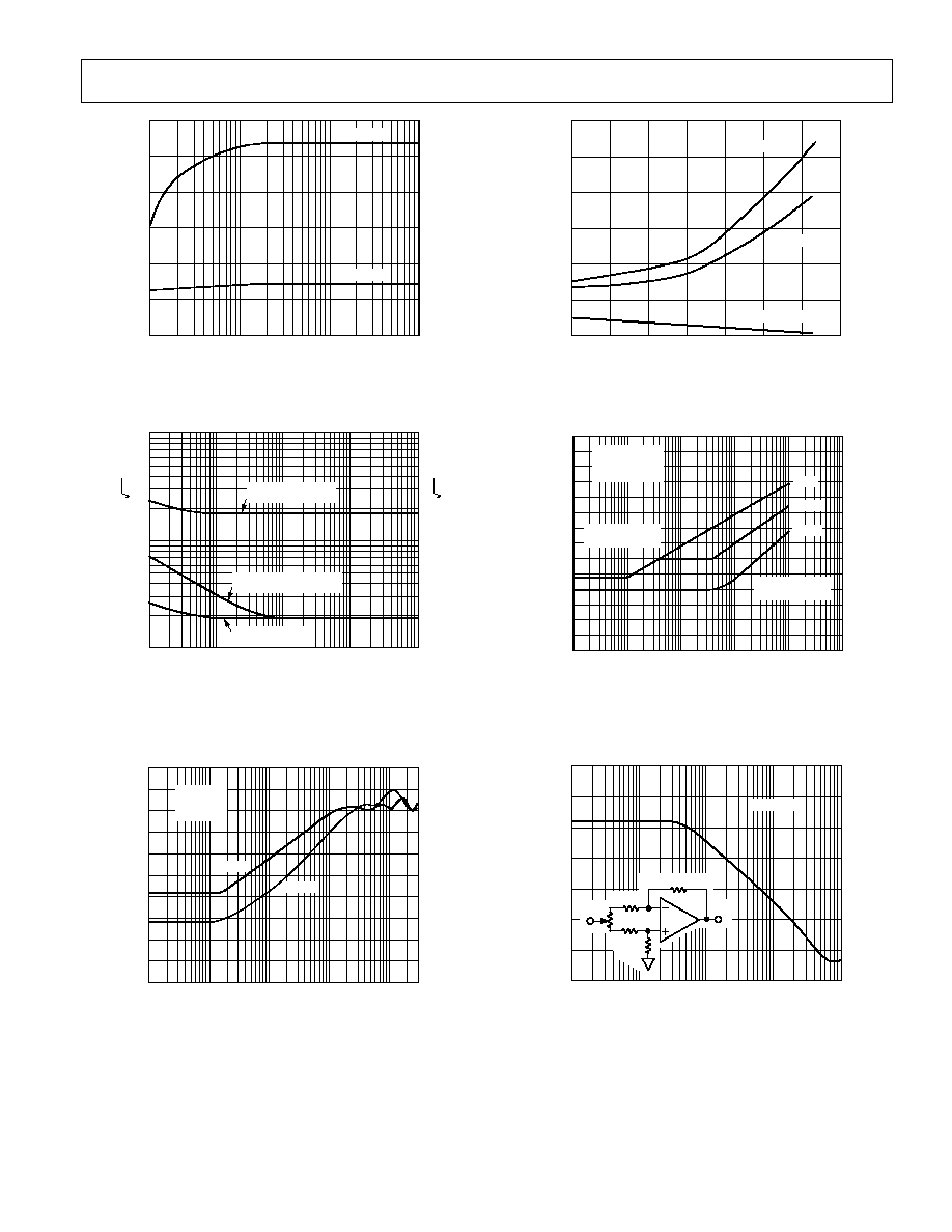
LOAD RESISTANCE (Differential ) (Single-Ended /2)
30
25
0
10
10k
100
1k
20
15
10
5
DIFFERENTIAL OUTPUT VOLTAGE Volts p-p
60
50
0
40
30
20
10
V
S
= 15V
V
S
= 5V
SINGLE-ENDED OUTPUT VOLTAGE Volts p-p
Figure 2. Driver Output Voltage Swing vs. Load Resistance
FREQUENCY Hz
100
10
1
10
100k
100
1k
10k
VOLTAGE NOISE nV
/
H
z
100
10
1
CURRENT NOISE pA/
H
z
INVERTING INPUT
CURRENT NOISE
NONINVERTING INPUT
CURRENT NOISE
INPUT VOLTAGE
NOISE
Figure 3. Driver Input Current and Voltage Noise vs.
Frequency
FREQUENCY MHz
0.01
0
10
20
30
40
50
60
70
80
90
100
0.1
PSRR dB
1
10
100
300
+PSRR
PSRR
V
S
= 15V
G = +2
R
L
= 100
Figure 4. Driver Power Supply Rejection vs. Frequency
5
REV. B
Typical Driver Performance CharacteristicsAD816
JUNCTION TEMPERATURE C
40
100
20
0
20
40
60
80
60
0
40
30
20
10
50
INPUT BIAS CURRENT
A
I
B
, V
S
= 15V
I
B
, V
S
= 5V
+I
B
, V
S
= 5V, 15V
Figure 5. Driver Input Bias Current vs. Temperature
FREQUENCY Hz
40
50
110
100
10M
1k
TOTAL HARMONIC DISTORTION dBc
10k
100k
1M
60
70
80
90
100
V
S
= 15V
G = +10
V
OUT
= 40V p-p
R
L
= 50
(DIFFERENTIAL)
R
L
=
200
(DIFFERENTIAL)
50
100
400
Figure 6. Driver Total Harmonic Distortion vs. Frequency
FREQUENCY Hz
80
10
10k
100M
100k
COMMON-MODE REJECTION dB
1M
10M
70
60
50
40
30
20
V
S
= 15V
1k
V
OUT
V
IN
1k
1k
1k
Figure 7. Driver Common-Mode Rejection vs. Frequency
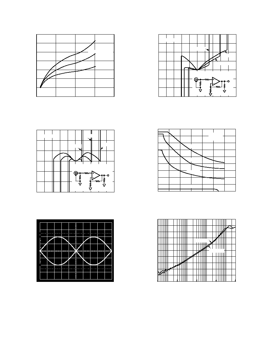
OUTPUT STEP SIZE V p-p
0
1400
1000
800
600
400
0
5
10
15
20
SINGLE-ENDED SLEW RATE V
/
s
(PER AMPLIFIER)
G = +5
R
L
= 100
SR
200
+SR
DIFFERENTIAL SR
1200
0
2800
2000
1600
1200
800
400
2400
DIFFERENTIAL SLEW RATE V
/
s
Figure 8. Driver Slew Rate vs. Output Step Size
V
OUT
Volts
15
0
15
20
20
16
12
8
4
0
4
8
12
16
10
5
5
10
V
S
= 10V
V
S
= 5V
RTI OFFSET mV
V
S
= 15V
T
A
= +25 C
1k
1k
R
L
=
25
V
OUT
100
49.9
V
I N
f = 0.1Hz
SINGLE
DRIVER
Figure 9. Driver Gain Nonlinearity vs. Output Voltage
10
0%
100
90
1 s
5V
Figure 10. Driver 40 V p-p Differential Sine Wave; R
L
= 50
,
f = 100 kHz
AD816Typical Driver Performance Characteristics
6
REV. B
LOAD CURRENT Amps
80
0
60
40
20
20
40
60
2.0
2.0
1.6
1.2
0.8
0.4
0
0.4
0.8
1.2
1.6
V
S
= 10V
V
S
= 5V
RTI OFFSET mV
V
S
= 15V
T
A
= +25 C
1k
1k
R
L
=
5
V
OUT
100
49.9
V
I N
f = 0.1Hz
SINGLE
DRIVER
Figure 11. Driver Thermal Nonlinearity vs. Output Current
Drive
FREQUENCY MHz
40
0
0
14
6
DIFFERENTIAL OUTPUT VOLTAGE V p-p
10
30
20
10
R
L
= 50
R
L
= 25
R
L
= 1
2
4
8
12
R
L
= 100
T
A
= +25 C
V
S
= 15V
Figure 12. Driver Large Signal Frequency Response
FREQUENCY Hz
100
30k
300M
100k
CLOSED-LOOP OUTPUT RESISTANCE
1M
10M
100M
10
1
0.1
0.01
300k
3M
30M
V
S
= 5V
V
S
= 15V
Figure 13. Driver Closed-Loop Output Resistance vs.
Frequency
AD816
REV. B
7
Typical Driver Characteristics
FREQUENCY Hz
100k
INPUT LEVEL dBV
OUTPUT LEVEL dBV
300M
1M
10M
100M
12
15
18
21
24
27
3
0
3
6
9
12
15
18
6
21
9
6
3
0
V
IN
= 0.5Vrms
V
IN
= 0.25Vrms
V
IN
= 125mVrms
V
IN
= 62.5mVrms
G = +2
R
F
= 499
R
L
= 100
R
S
= 100
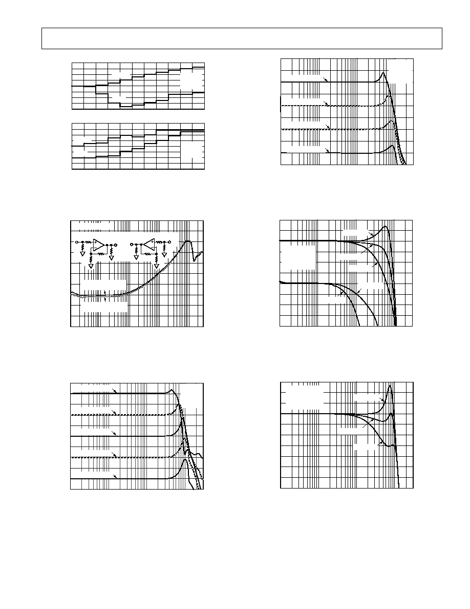
Figure 17. Driver Small and Large Signal Frequency
Response, G = +2
FREQUENCY Hz
100k
300M
1M
NORMALIZED FLATNESS dB
10M
100M
0.1
0
0.1
0.2
0.3
0.4
V
IN
= 50mVrms
G +5
R
L
= 100
R
S
= 100
0
1
2
3
4
5
6
7
1
2
8
NORMALIZED FREQUENCY RESPONSE dB
R
F
= 499
R
F
= 604
R
F
= 750
R
F
= 604
R
F
= 750
Figure 18. Driver Frequency Response and Flatness,
G = +5
FREQUENCY Hz
100k
300M
1M
10M
100M
V
IN
= 200mVrms
G +2
R
L
= 100
R
S
= 100
0
1
2
3
4
5
6
7
1
2
3
R
F
= 499
R
F
= 750
R
F
= 604
NORMALIZED FREQUENCY RESPONSE dB
Figure 19. Driver Frequency Response vs. R
F
, G = +2
0.04
0.03
0.02
0.01
0.00
0.01
0.02
0.03
0.04
DIFF GAIN %
0.12
0.10
0.08
0.06
0.04
0.02
0.00
0.02
0.04
DIFF PHASE De
g
rees
G = +2
R
F
= 1k
NTSC
1
2
3
4
5
6
7
8
9
10
11
0.5
0.4
0.3
0.2
0.1
0.0
0.1
0.2
0.3
GAIN
PHASE
0.005
0.000
0.005
0.010
0.015
0.020
0.025
0.030
0.010
DIFF GAIN %
DIFF PHASE Degrees
1
2
3
4
5
6
7
8
9
10
11
6 BACK TERMINATED LOADS (25 )
2 BACK TERMINATED LOADS (75 )
G = +2
R
F
= 1k
NTSC
GAIN
PHASE
Figure 14. Driver Differential Gain and Differential
Phase (Per Amplifier)
FREQUENCY Hz
10k
100k
1M
10M
100M 300M
0
10
20
30
40
50
60
70
80
90
CROSSTALK dB
DRIVER B = INPUT
DRIVER A = OUTPUT
100
DRIVER A = INPUT
DRIVER B = OUTPUT
V
IN
= 200mVrms
499
100
100
50
OUTPUT
INPUT
499
DRIVER
A
499
100
100
50
OUTPUT
INPUT
499
DRIVER
B
Figure 15. Driver Output-to-Output Crosstalk vs.
Frequency
FREQUENCY Hz
100k
1M
10M
100M
300M
3
0
3
6
9
12
15
18
21
24
OUTPUT/
INPUT
LEVEL
d
B
V
27
V
IN
= 1.0Vrms
V
IN
= 0.5Vrms
V
IN
= 0.25Vrms
V
IN
= 125mVrms
V
IN
= 62.5mVrms
G = +1
R
F
= 499
R
L
= 100
R
S
= 100
Figure 16. Driver Small and Large Signal Frequency
Response, G = +1
AD816Typical Driver Performance Characteristics
8
REV. B
AD816
DRIVER A/B
8
0.1 F
10 F
+15V
0.1 F
10 F
7
15V
R
L
= 100
100
55
V
IN
PULSE
GENERATOR
T
R
/T
F
= 250ps
1k
1k
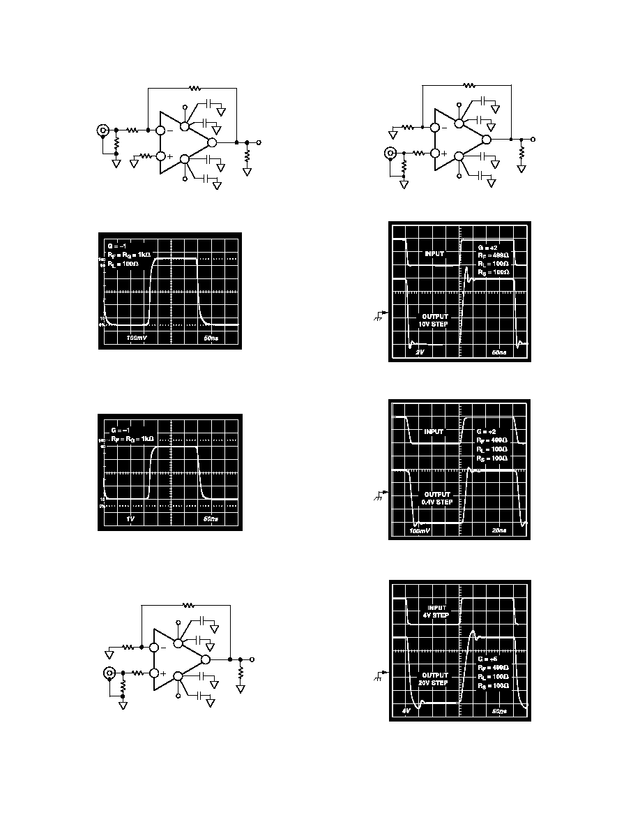
Figure 20. Test Circuit Gain = 1
Figure 21. Driver 500 mV Step Response, G = 1
Figure 22. Driver 4 V Step Response, G = 1
8
0.1 F
10 F
+15V
0.1 F
10 F
7
15V
R
L
= 100
100
50
V
IN
PULSE
GENERATOR
T
R
/T
F
= 250ps
R
G
R
F
AD816
DRIVER A/B
Figure 23. Test Circuit, Gain = 1 + R
F
/R
G
0.1 F
10 F
+15V
499
0.1 F
10 F
7
15V
R
L
= 100
100
50
V
IN
PULSE
GENERATOR
T
R
/T
F
= 500ps
8
AD816
DRIVER A/B
499
Figure 24. Driver Test Circuit, Gain = +2
Figure 25. 10 V Step Response, G = +2
Figure 26. Driver 400 mV Step Response, G = +2
Figure 27. Driver 20 V Step Response, G = +5
Typical Receiver Performance CharacteristicsAD816
REV. B
9
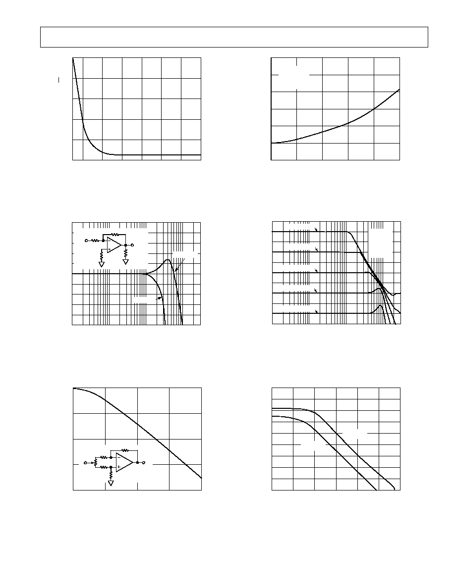
FREQUENCY Hz
50
40
0
3
10M
10
100
1k
10k
100k
1M
30
20
10
INPUT VOLTAGE NOISE nV/
Hz
Figure 28. Receiver Input Voltage Noise Spectral Density
FREQUENCY Hz
100k
300M
1M
10M
100M
1
0
1
2
3
4
5
2
3
4
5
GAIN dB
100
1k
50
V
OUT
V
IN
1k
V
S
= 5V
V
S
= 15V
Figure 29. Receiver Closed-Loop Gain vs. Frequency,
Gain = 1
FREQUENCY Hz
100
80
0
1k
10M
10k
CMR dB
100k
1M
60
40
1k
1k
V
OUT
V
IN
1k
1k
Figure 30. Receiver Common-Mode Rejection vs.
Frequency
FREQUENCY Hz
40
50
100
100
10M
1k
HARMONIC DISTORTION dB
10k
100k
1M
60
70
80
90
G = +5
V
OUT
= 14V p-p
R
F
= 4k
R
L
= 1k
Figure 31. Receiver Harmonic Distortion vs. Frequency
FREQUENCY Hz
100k
300M
1M
INPUT LEVEL dBV
10M
100M
G = +2
R
F
= 1k
C
F
= 2.2pF
R
L
= 100
R
S
= 0
3
0
3
6
9
12
15
18
6
9
21
OUTPUT LEVEL
(
RTO
)
dBV
3
6
9
12
15
18
21
24
0
3
27
V
IN
= 0.5Vrms
V
IN
= 1.0Vrms
V
IN
= 0.25Vrms
V
IN
= 0.0625Vrms
V
IN
= 0.125Vrms
Figure 32. Receiver Small and Large Signal Frequency
Response, Gain = +2
FREQUENCY Hz
100
1k
10k
100k
1M
10M
100M
100
90
10
50
40
30
20
70
60
80
PSR dB
POSITIVE
SUPPLY
NEGATIVE
SUPPLY
Figure 33. Receiver Power Supply Rejection vs. Frequency
REV. B
AD816Typical Receiver Performance Characteristics
AD816
REC A/B
8
0.1 F
10 F
+15V
10 F
7
15V
R
L
50
V
IN
PULSE
GENERATOR
T
R
/ T
F
= 500ps
1k
1k
0.1 F
2.2pF
V
OUT
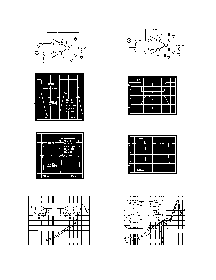
Figure 34. Test Circuit, Gain = +2
Figure 35. Receiver 10 V Step Response, G = +2
Figure 36. Receiver 400 mV Step Response, G = +2
FREQUENCY MHz
0.1
300
CROSSTALK dB
1
10
100
40
50
60
70
80
90
100
30
20
10
0
0.01
RECEIVER A = INPUT
RECEIVER B = OUTPUT
RECEIVER B : INPUT
RECEIVER A : OUTPUT
V
IN
= 200mVrms
1k
100
50
OUTPUT
INPUT
1k
REC A
2.2pF
1k
100
50
OUTPUT
INPUT
1k
REC B
2.2pF
Figure 37. Receiver Output-to-Output Crosstalk
vs. Frequency
10
AD816
REC A/B
8
0.1 F
10 F
+15V
10 F
7
15V
R
L
= 500
50
V
IN
PULSE
GENERATOR
T
R
/ T
F
= 250ps
1k
1k
0.1 F
V
OUT
Figure 38. Test Circuit, Gain = 1
5V
50ns
Figure 39. Receiver 10 V Step Response, G = 1
50ns
Figure 40. Receiver 400 mV Step Response, G = 1
FREQUENCY MHz
0.1
300
1
10
100
40
50
60
70
80
90
100
30
20
10
0
CROSSTALK dB
0.01
DRIVER A: INPUT
RECEIVER B: OUTPUT
V
IN
= 200mVrms
DRIVER B: INPUT
RECEIVER A: OUTPUT
DRIVER A: INPUT
RECEIVER A: OUTPUT
DRIVER B: INPUT
RECEIVER A: OUTPUT
499
100
50
INPUT
499
DRV A
100
OUTPUT
1k
100
50
OUTPUT
INPUT
1k
2.2pF
REC A
499
100
50
OUTPUT
INPUT
499
DRV B
100
1k
100
50
OUTPUT
INPUT
1k
REC B
2.2pF
Figure 41. Driver-to-Receiver Crosstalk vs. Frequency
AD816
REV. B
11
Table I. Driver Resistor Values
R
F
( )
R
G
( )
G = +1
604
1
499
499
+2
499
499
+5
499
125
+10
1k
110
DRIVER DC ERRORS AND NOISE
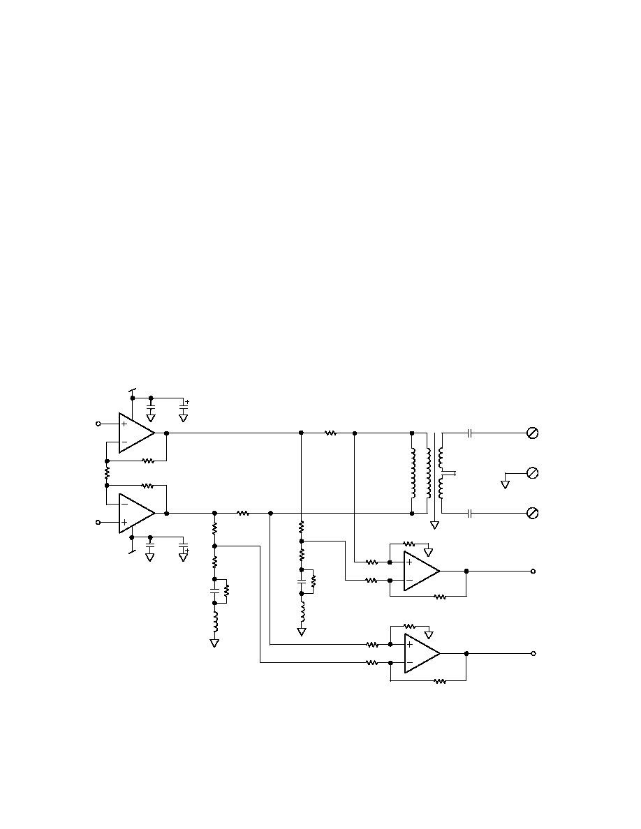
There are three major noise and offset terms to consider in a
current feedback amplifier. For offset errors refer to the equa-
tion below. For noise error the terms are root-sum-squared to
give a net output error. In the circuit below (Figure 43), they
are input offset (V
IO
) which appears at the output multiplied by
the noise gain of the circuit (1 + R
F
/R
G
), noninverting input
current (I
BN
×
R
N
) also multiplied by the noise gain, and the
inverting input current, which when divided between R
F
and R
G
and subsequently multiplied by the noise gain always appear at
the output as I
BI
×
R
F
. The input voltage noise of the AD816 is
less than 4 nV/
Hz. At low gains, however, the inverting input
current noise times R
F
is the dominant noise source. Careful
layout and device matching contribute to better offset and drift.
The typical performance curves in conjunction with the equations
below can be used to predict the performance of the AD816 in
any application.
V
OUT
=
VIO 1
+
R
F
R
G
±
I
BN
R
N
1
+
R
F
R
G
±
I
BI
R
F
I
B I
I
B N
R
G
R
N
R
F
V
OUT
VIO
AD816
DRIVERS
Figure 43. Driver Output Offset Voltage
THEORY OF OPERATION (RECEIVER)
Each AD816 receiver is a wide band high performance opera-
tional amplifier. It also provides a constant slew rate, bandwidth
and settling time over its entire specified temperature range.
The AD816 receiver consists of a degenerated NPN differential
pair driving matched PNPs in a folded-cascode gain stage. The
output buffer stage employs emitter followers in a class AB
amplifier which deliver the necessary current to the load while
maintaining low levels of distortion.
A protection resistor in series with the noninverting input is
required in circuits where the input to the receiver could be
subject to transients on continuous overload voltages exceeding
the
±
6 V maximum differential limit. The resistor provides
protection for the input transistors, by limiting their maximum
base current.
THEORY OF OPERATION (DRIVER)
The AD816 driver is a dual current feedback amplifier with high
(500 mA) output current capability. Being a current feedback
amplifier, the AD816 driver's open-loop behavior is expressed
as transimpedance,
V
O
/
I
IN
, or T
Z
. The open-loop trans-
impedance behaves just as the open-loop voltage gain of a volt-
age feedback amplifier, that is, it has a large dc value and de-
creases at roughly 6 dB/octave in frequency.
Since R
IN
is proportional to 1/g
M
, the equivalent voltage gain is
just T
Z
×
g
M
, where the g
M
in question is the transconductance
of the input stage. Figure 42 shows the driver connected as a
follower with gain. Basic analysis yields the following results:
V
O
V
IN
=
G
×
T
Z
S
( )
T
Z
S
( )
+
G
×
R
IN
+
R
F
where:
G =
1
+
R
F
R
G
R
IN
= 1/g
M
25
R
IN
V
IN
R
F
V
OUT
R
G
R
N
Figure 42. Current-Feedback Amplifier Operation
Recognizing that G
×
R
IN
<< R
F
for low gains, it can be seen to
the first order that bandwidth for this amplifier is independent
of gain (G).
Considering that additional poles contribute excess phase at
high frequencies, there is a minimum feedback resistance below
which peaking or oscillation may result. This fact is used to
determine the optimum feedback resistance, R
F
. In practice
parasitic capacitance at the inverting input terminal will also add
phase in the feedback loop so that picking an optimum value for
R
F
can be difficult.
Achieving and maintaining gain flatness of better than 0.1 dB at
frequencies above 10 MHz requires careful consideration of
several issues.
Choice of Feedback and Gain Resistors
The fine scale gain flatness will, to some extent, vary with
feedback resistance. It is therefore recommended that once
optimum resistor values have been determined, 1% tolerance
values should be used if it is desired to maintain flatness over a
wide range of production lots. Table I shows optimum values
for several useful gain configurations. These should be used as a
starting point in any application.
AD816
REV. B
12
PRINTED CIRCUIT BOARD LAYOUT
CONSIDERATIONS
As to be expected for a wideband amplifier, PC board parasitics
can affect the overall closed-loop performance. Of concern are
stray capacitances at the output and the inverting input nodes. If
a ground plane is to be used on the same side of the board as
the signal traces, a space (5 mm min) should be left around the
signal lines to minimize coupling.
POWER SUPPLY BYPASSING
Adequate power supply bypassing can be critical when optimiz-
ing the performance of a high frequency circuit. Inductance in
the power supply leads can form resonant circuits that produce
peaking in the amplifier's response. In addition, if large current
transients must be delivered to the load, then bypass capacitors
(typically greater than 1
µ
F) will be required to provide the best
settling time and lowest distortion. A parallel combination of
10.0
µ
F and 0.1
µ
F is recommended. Under some low frequency
applications, a bypass capacitance of greater than 10
µ
F may be
necessary. Due to the large load currents delivered by the AD816,
special consideration must be given to careful bypassing. The
ground returns on both supply bypass capacitors as well as signal
common must be "star" connected as shown in Figure 44.
R
F
R
G
(OPTIONAL)
R
F
+V
S
+OUT
OUT
V
S
+IN
IN
DRIVER A
DRIVER B
R
F
R
G
R
F
R
G
IN
IN
RECEIVER A
RECEIVER B
OUT
OUT
Figure 44. Signal Ground Connected in "Star"
Configuration
POWER CONSIDERATIONS
The 500 mA drive capability of the AD816 driver enables it to
drive a 50
load at 40 V p-p when it is configured as a dif-
ferential driver. This implies a power dissipation, P
IN
, of nearly
5 watts. To ensure reliability, the junction temperature of the
AD816 should be maintained at less than 175
°
C. For this rea-
son, the AD816 will require some form of heat sinking in most
applications. The thermal diagram of Figure 45 gives the basic
relationship between junction temperature (T
J
) and various
components of
JA
.
T
J
=
T
A
+
P
IN
JA
Equation 1
A
(JUNCTION TO
DIE MOUNT)
B
(DIE MOUNT
TO CASE)
A
+
B
=
JC
CASE
T
A
T
J
JC
CA
T
A
JA
T
J
P
IN
WHERE:
P
IN
= DEVICE POWER DISSIPATION
T
A
= AMBIENT TEMPERATURE
T
J
= JUNCTION TEMPERATURE
JC
= THERMAL RESISTANCE JUNCTION TO CASE
CA
= THERMAL RESISTANCE CASE TO AMBIENT
Figure 45. A Breakdown of Various Package Thermal
Resistances
Figure 46 gives the relationship between output voltage swing
into various loads and the power dissipated by the AD816 (P
IN
).
This data is given for both sine wave and square wave (worst
case) conditions. It should be noted that these graphs are for
mostly resistive (phase <
±
10
°
) loads. When the power dissipation
requirements are known, Equation 1 and the graph on Figure 47
can be used to choose an appropriate heat sinking configuration.
4
3
P
IN
Watts
10
20
30
40
2
1
V
OUT
Volts p-p
R
L
= 50
R
L
= 100
R
L
= 200
f = 1kHz
SQUARE WAVE
SINE WAVE
V
S
= 15V
Figure 46. Total Power Dissipation vs Differential Driver
Output Voltage
AD816
REV. B
13
Normally, the AD816 will be soldered directly to a copper pad.
Figure 47 plots
JA
against size of copper pad. This data pertains
to copper pads on both sides of G10 epoxy glass board connected
together with a grid of feedthroughs on 5 mm centers.
This data shows that loads of 100 ohms or greater will usually
not require any more than this. This is a feature of the AD816's
15-lead power SIP package.
An important component of
JA
is the thermal resistance of the
package to heatsink. The data given is for a direct soldered
connection of package to copper pad. The use of heatsink
grease either with or without an insulating washer will increase
this number. Several options now exist for dry thermal connec-
tions. These are available from Bergquist as part # SP600-90.
Consult with the manufacturer of these products for details of
their application.
COPPER HEAT SINK AREA (TOP AND BOTTOM) mm
2
35
30
10
0
2.5k
0.5k
JA
C/W
1k
1.5k
2k
25
20
15
AD816AVR, AY
(
JC
= 2 C/W)
1
2
3
COPPER HEAT SINK AREA (TOP AND BOTTOM) in
2
Figure 47. Power Package Thermal Resistance vs. Heat
Sink Area
Other Power Considerations
There are additional power considerations applicable to the
AD816. First, as with many current feedback amplifiers, there is an
increase in supply current when delivering a large peak-to-peak
voltage to a resistive load at high frequencies. This behavior is
affected by the load present at the amplifier's output. Figure 12
summarizes the full power response capabilities of the AD816
driver. These curves apply to the differential driver applications
(right-hand side of Figure 52). In Figure 12, maximum continu-
ous peak-to-peak output voltage is plotted vs. frequency for
various resistive loads. Exceeding this value on a continuous
basis can damage the AD816.
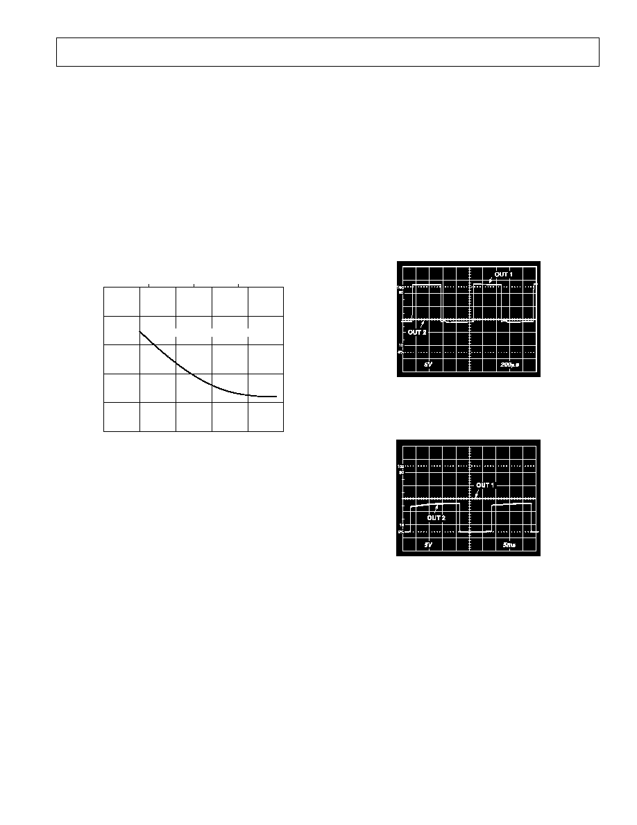
The AD816 is equipped with a thermal shutdown circuit. This
circuit ensures that the temperature of the AD816 die remains
below a safe level. In normal operation, the circuit shuts down
the AD816 at approximately 180
°
C and allows the circuit to
turn back on at approximately 140
°
C. This built-in hysteresis
means that a sustained thermal overload will cycle between
power-on and power-off conditions. The thermal cycling typi-
cally occurs at a rate of 1 ms to several seconds, depending on
the power dissipation and the thermal time constants of the
package and heat sinking. Figures 48 and 49 illustrate the ther-
mal shutdown operation after driving OUT1 to the + rail, and
OUT2 to the rail, and then short-circuiting to ground each
output of the AD816. The AD816 will not be damaged by
momentary operation in this state, but the overload condition
should be removed.
Figure 48. OUT2 Shorted to Ground Through a 2
Resistor, Square Wave Is OUT1, R
F
= 1 k
, R
G
= 222
Figure 49. OUT1 Shorted to Ground Through a 2
Resistor, Square Wave Is OUT2, R
F
= 1 k
, R
G
= 222
AD816
REV. B
14
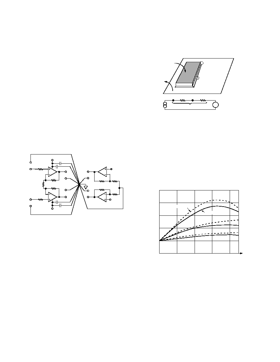
APPLICATIONS
ADSL Transceiver
The AD816 is designed for the primary purpose of providing an
integrated solution for the transmit and receive functions of an
ADSL modem. ADSL or Asymmetrical Digital Subscriber Line
is a means for delivering up to 6 Mbps from a telephone central
office (CO) into a home over the conventional telephone twisted
pair (local loop) and a few hundred kbps simultaneously in the
opposite direction.
The transmit/receive block is commonly referred to as a hybrid,
which is an old telephone term, and the function was originally
performed with passive circuitry in early phone systems. The
hybrid's function is to deliver maximum transmit power down
the line, while providing the receive circuitry with a maximum
receive signal and a minimized (self) transmit signal. As the line
gets longer, this separation becomes much more difficult, be-
cause the transmit signal must be larger to reach the other end
with acceptable SNR, while the receive signal is more attenu-
ated by the longer line.
The figure of merit for the performance of the hybrid is com-
monly called trans-hybrid loss and is a measure of how much
the transmit signal that appears in the receive circuit has been
attenuated relative to the amplitude of the transmit signal itself.
It is measured in dBs and is a function of frequency.
In addition to the passive circuits that have been used over time,
active circuit techniques can enhance the hybrid's performance.
Figure 50 shows one of the various hybrid circuits that uses the
AD816 in an ADSL application. The high power op amps serve
as the transmitter, while the low noise amplifiers serve as the
receiver.
The power amplifiers of the AD816 (D1 and D2) are arranged
in a differential configuration that receives its inputs from the
differential outputs of a D/A converter. The outputs differen-
tially drive the transformer primary with a turns ratio of 1:2.
The line on the secondary side of the transformer has an imped-
ance of 120
. Thus one quarter of this resistance (30
) is
required for back termination on the primary side due to the
impedance scaling by the square of the turns ratio. This resis-
tance is divided in half (15
) and put on each side of the drive
buffers for symmetry (R101 and R201).
The receive section (R1 and R2) is configured as a pair of differ-
ence amplifiers that together produce a differential output that
consists of the receive signal in addition to the transmit signal
attenuated by the trans-hybrid loss.
The circuit is highly symmetrical, so a single-ended explanation
can be easily generalized to understand the differential opera-
tion. D1 output terminals (Pin 6 of the AD816) drives the top
of the primary of T1 through R101. A voltage divider is formed
+15V
0.1 F
10 F
8
6
715
4
5
15V
7
9
715
11
10
D1
AD816
806
V+
V
R202
196
R203
196
R204
1.18k
L201
12 H
R201
15
R101
15
2
3
1
R106
348
R105
162
R107
1k
R108
2.37k
RCV OUT+
1
2
4
10
9
6
8
7
5
T1
XFRMR
C601
0.1 F
C602
0.1 F
TELEPHONE
TWISTED PAIR
D2
0.1 F
10 F
R102
196
R103
196
R104
1.18k
C101
8.2 F
L101
12 H
R1
AD816
13
12
14
R206
348
R205
162
R207
1k
R208
2.37k
RCV OUT
R2
AD816
C201
8.2 F
Figure 50. AD816 as an ADSL Transceiver
AD816
REV. B
15
by R101 and all the downstream circuitry comprised of T1, the
transmission line and its termination. For an ideal transformer,
transmission line and termination, this will appear to be 15
,
and thus the signal appearing at Pins 1 and 2 of T1 will be the
output of D1 divided by two in the ideal case. This signal is
applied to the input of R1 (Receive 1 of the AD816) (Pin 3) via
R105.
In some ADSL systems (DMT), there is a need to transmit
higher crest factor signals. Typically this is done by increasing
the turns ratio of T1 to as much as 4:1. In this case, R101 and
R201 would be 3.75
, and the peak current of the AD816
(1 A) would be the drive limit of the transmitter.
R1 is configured as a difference amplifier. The negative side
(Pin 2) is driven by another signal that is a divided down version
of the output of D1. This circuit is formed by R102 as one side
of the voltage divider along with R103, C101, R104 and L101
as the other half of the divider. If the frequency dependent
impedance part of this circuit matches the transformer, trans-
mission line and termination impedance, then the signals
applied to both sides of the difference-amp-configured R1 will
be the same, and the transmit signal will be totally subtracted
out by the circuit.
In a real-world situation, it is not practical (or even possible) to
subtract out all of the transmit signal (100% trans-hybrid loss),
but only provide a first order cancellation which goes a long way
toward reducing the dynamic range of the RCVOUT signal.
The overall performance of this circuit depends on the ability to
build a lumped element network that matches the impedance of
the transmission line over the frequency range required for
ADSL (
20 kHz to 1.1 MHz).
The circuits formed by D2 and R2 of the AD816 are totally
symmetric with those formed by D1 and R1 and work in the
same fashion. All the components in the D1, R1 circuits that are
numbered with 100 range numbers are numbered with 200
range numbers in the D2, R2 circuits.
The receive signal from the telephone line creates a differential
signal across the primary of T1. There is, however, a two to one
reduction in amplitude due to turns ratio of T1. This differen-
tial signal is applied to the + inputs (Pins 3 and 12) of R1 and
R2. The receive amplifiers buffer this signal and present a differ-
ential output at Pins 1 and 14. There is no significant receive
signal applied to the negative inputs of R1 and R2 due to the
attenuating effects of R101 and R201 and the low output
impedances of D1 and D2.
Thus, the overall circuit provides first order cancellation of the
transmit signal and differential buffering of the receive signal.
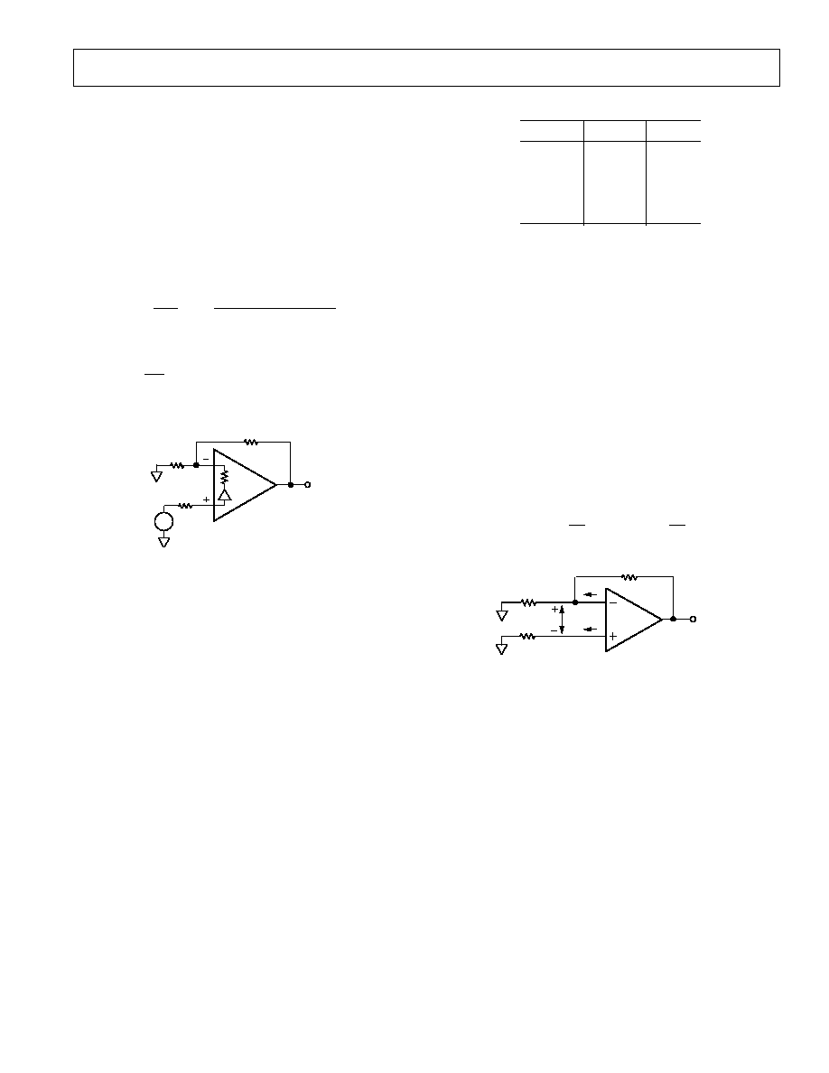
Dual Composite Amplifier
A composite amplifier uses two different op amps together in a
circuit to yield an overall performance that has some of the
advantages of each op amp. In the case of the AD816, two com-
posite amplifiers can be constructed that offer the low noise of
the receiver amps in addition to the high current output of the
driver amps.
The circuit in Figure 51 shows an example of such a circuit. It
uses receiver amp R1 for the low noise first stage and driver D1
for the high output current second stage. Both local and overall
feedback are used to get the desired response.
6
4
5
V
OUT
2
3
R1
D1
V
IN
Figure 51. AD816 Composite Amplifier
Creating Differential Signals
If only a single-ended signal is available to drive the AD816 and
a differential output signal is desired, a circuit can be used to
perform the single-ended to differential conversion.
The circuit shown in Figure 52 performs this function. It uses
the AD816 with the gain of one receiver set at +1 and the gain
of the other at 1. The 1 k
resistor across the input terminals
of the follower makes the noise gain (NG = 2) equal to the
inverter's. The two receiver outputs then differentially drive the
inputs to the AD816 driver with no common-mode signal to first
order.
6
4
5
8
+15V
10
7
15V
R
F
499
R
L
9
11
0.1 F
10 F
R
G
100
R
F
499
0.1 F
10 F
1
8
+15V
0.1 F
2
1k
4
15V
1k
7
0.1 F
6
5
1k
3
AD816
100
100
1k
AD816
AD816
AD816
RECEIVER #1
RECEIVER #2
DRIVER #1
DRIVER #2
Figure 52. Differential Driver with Single-Ended
Differential Converter
AD816
REV. B
16
C2191b012/99 (rev. B)
PRINTED IN U.S.A.
15-Lead Surface Mount DDPAK
(VR-15)
1
0.080 (2.03)
0.065 (1.65)
2 PLACES
0.694 (17.63)
0.684 (17.37)
PIN 1
0.516
(13.106)
0.110
(2.79)
BSC
0.042
(1.066)
TYP
0.137
(3.479)
TYP
0.394
(10.007)
0.152 (3.86)
0.148 (3.76)
0.600 (15.24)
BSC
0.079 (2.006)
DIA
2 PLACES
15
0.024 (0.61)
0.014 (0.36)
0.063 (1.60)
0.057 (1.45)
8
°
0
°
0.088 (2.24)
0.068 (1.72)
0.426 (10.82)
0.416 (10.57)
SEATING
PLANE
0.031 (0.79)
0.024 (0.60)
0.100 (2.54)
BSC
0.798 (20.27)
0.778 (19.76)
0.182 (4.62)
0.172 (4.37)
0.146 (3.70)
0.138 (3.50)
15-Lead Through-Hole SIP with Staggered Leads
and 90 Lead Form
(Y-15)
0.063 (1.60)
0.057 (1.45)
0.671
±
0.006
(17.043
±
0.152)
SHORT
LEAD
0.024 (0.61)
0.014 (0.36)
0.666
±
0.006
(16.916
±
0.152)
LONG
LEAD
0.691
±
0.010
(17.551
±
0.254)
0.766
±
0.010
(19.456
±
0.254)
0.791
±
0.010
(20.091
±
0.254)
0.694 (17.63)
0.684 (17.37)
PIN 1
0.110
(2.79)
BSC
0.394
(10.007)
0.152 (3.86)
0.148 (3.76)
0.080 (2.03)
0.065 (1.65)
2 PLACES
0.516 (
1
3.106)
0.042
(1.066)
TYP
0.137
(3.479)
TYP
0.079
(2.006) DIA
2 PLACES
0.426 (10.82)
0.416 (10.57)
1
15
0.700 (17.78) BSC
SEATING
PLANE
0.031 (0.79)
0.024 (0.60)
0.050
(1.27)
BSC
0.798 (20.27)
0.778 (19.76)
0.182 (4.62)
0.172 (4.37)
0.209
±
0.010
(5.308
±
0.254)
OUTLINE DIMENSIONS
Dimensions shown in inches and (mm).
15-Lead Through-Hole SIP with Staggered Leads
and Straight Lead Form
(YS-15)
0.080 (2.03)
0.065 (1.65)
2 PLACES
0.694 (17.63)
0.684 (17.37)
PIN 1
0.110
(2.79)
BSC
0.042
(1.07)
TYP
0.137
(3.48)
TYP
0.394
(10.007)
0.152 (3.86)
0.148 (3.76)
0.700 (17.78) BSC
0.079
(2.007) DIA
2 PLACES
0.426 (10.82)
0.416 (10.57)
0.
516 (13.
1
06)
1
15
0.063 (1.60)
0.057 (1.45)
0.627
±
0.010
(15.926
±
0.254)
SHORT
LEAD
0.601
±
0.010
(15.265
±
0.254)
LONG
LEAD
0.176 (4.47)
0.150 (3.81)
0.710 (18.03)
0.690 (17.53)
0.200
(5.08)
BSC
0.169
(4.29)
BSC
0.024 (0.61)
0.014 (0.36)
0.031 (0.79)
0.024 (0.60)
0.050 (1.27)
BSC
0.798 (20.27)
0.778 (19.76)
0.182 (4.62)
0.172 (4.37)
SEATING
PLANE