 | ÐлекÑÑоннÑй компоненÑ: AD8221 | СкаÑаÑÑ:  PDF PDF  ZIP ZIP |
Äîêóìåíòàöèÿ è îïèñàíèÿ www.docs.chipfind.ru
Precision Instrumentation Amplifier
AD8221
Rev. A
Information furnished by Analog Devices is believed to be accurate and reliable.
However, no responsibility is assumed by Analog Devices for its use, nor for any
infringements of patents or other rights of third parties that may result from its use.
Specifications subject to change without notice. No license is granted by implication
or otherwise under any patent or patent rights of Analog Devices. Trademarks and
registered trademarks are the property of their respective owners.
One Technology Way, P.O. Box 9106, Norwood, MA 02062-9106, U.S.A.
Tel: 781.329.4700
www.analog.com
Fax: 781.326.8703
© 2003 Analog Devices, Inc. All rights reserved.
FEATURES
Available in space-saving MSOP package
Gain set with 1 external resistor (gain range 1 to 1000)
Wide power supply range:
±2.3 V to ±18 V
Temperature range for specified performance:
40°C to +85°C
Operational up to 125°C
1
EXCELLENT AC SPECIFICATONS
80 dB min CMRR to 10 kHz ( G = 1)
825 kHz 3 dB bandwidth (G = 1)
2 V/µs slew rate
LOW NOISE
8 nV/Hz, @ 1 kHz, max input voltage noise
0.25 µV p-p input noise (0.1 Hz to 10 Hz)
HIGH ACCURACY DC PERFORMANCE (AD8221BR)
90 dB min CMRR (G = 1)
25 µV max input offset voltage
0.3 µV/°C max input offset drift
0.4 nA max input bias current
APPLICATIONS
Weigh scales
Industrial process controls
Bridge amplifiers
Precision data acquisition systems
Medical instrumentation
Strain gages
Transducer interfaces
GENERAL DESCRIPTION
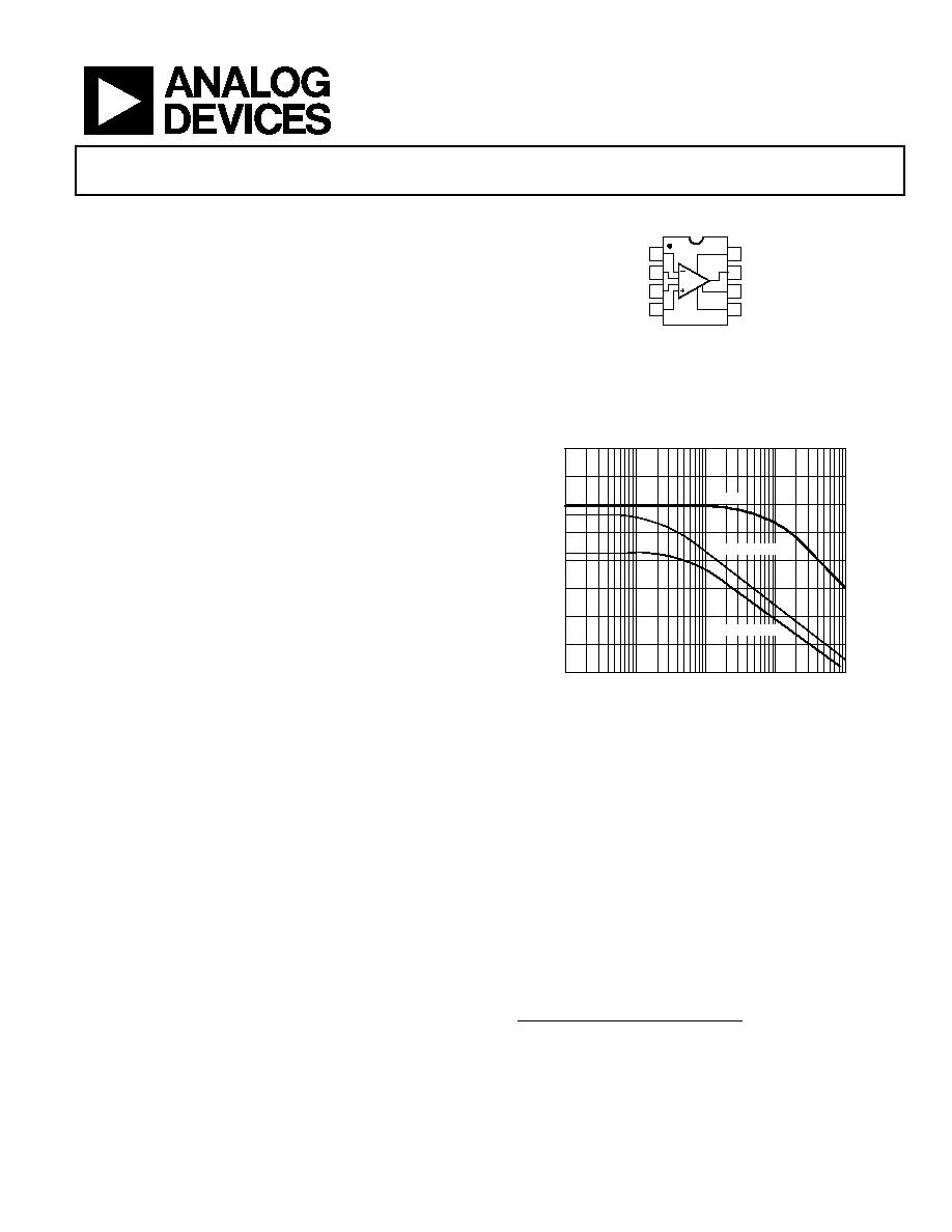
The AD8221 is a gain programmable, high performance instru-
mentation amplifier that delivers the industry's highest CMRR
over frequency. The CMRR of instrumentation amplifiers on
the market today falls off at 200 Hz. In contrast, the AD8221
maintains a minimum CMRR of 80 dB to 10 kHz for all grades
at G = 1. High CMRR over frequency allows the AD8221 to
reject wideband interference and line harmonics, greatly
simplifying filter requirements. Possible applications include
precision data acquisition, biomedical analysis, and aerospace
instrumentation.
Low voltage offset, low offset drift, low gain drift, high gain
accuracy, and high CMRR make this part an excellent choice in
applications that demand the best dc performance possible,
such as bridge signal conditioning.
CONNECTION DIAGRAM
8
7
6
5
1
2
3
4
IN
R
G
R
G
+V
S
V
OUT
REF
V
S
+IN
TOP VIEW
AD8221
03149-0-001
Figure 1. SOIC and MSOP Connection Diagram
40
50
60
70
80
90
CMRR (dB)
100
110
120
FREQUENCY (Hz)
100
10
1k
10k
100k
03149-0-002
AD8221
COMPETITOR 1
COMPETITOR 2
Figure 2. Typical CMRR vs. Frequency for G = 1
Programmable gain affords the user design flexibility. A single
resistor sets the gain from 1 to 1000. The AD8221 operates on
both single and dual supplies, and is well suited for applications
where ±10 V input voltages are encountered.
The AD8221 is available in low cost 8-lead SOIC and MSOP
packages, both of which offer the industry's best performance.
The MSOP requires half the board space of the SOIC, making it
ideal for multichannel or space-constrained applications.
Performance is specified over the entire industrial temperature
range of 40°C to +85°C for all grades. Furthermore, the
AD8221 is operational from 40°C to +125°C
1
.
1
See Typical Performance Curves for expected operation from 85°C to 125°C.

AD8221
Rev. A | Page 2 of 20
TABLE OF CONTENTS
Specifications..................................................................................... 3
Absolute Maximum Ratings............................................................ 5
ESD Caution.................................................................................. 5
Typical Performance Characteristics ............................................. 6
Theory of Operation ...................................................................... 13
Gain Selection ............................................................................. 14
Layout........................................................................................... 14
Reference Terminal .................................................................... 15
Power Supply Regulation and Bypassing ................................ 15
Input Bias Current Return Path................................................ 15
Input Protection ......................................................................... 15
RF Interference ........................................................................... 16
Precision Strain Gage................................................................. 16
Conditioning ±10 V Signals for a +5 V Differential Input
ADC ............................................................................................. 17
AC-Coupled Instrumentation Amplifier ................................ 17
Outline Dimensions ....................................................................... 18
Ordering Guide .......................................................................... 18
REVISION HISTORY
Revision A
11/03--Data Sheet Changed from Rev. 0 to Rev. A
Change Page
Changes to Features...............................................................................1
Changes to Specifications section .......................................................4
Change to Theory of Operation section...........................................13
Change to Gain Selection section......................................................14

AD8221
Rev. A | Page 3 of 20
SPECIFICATIONS
Table 1. V
S
= ±15 V, V
REF
= 0 V, T
A
= +25°C, G = 1, R
L
= 2 k, unless otherwise noted
AR Grade
BR Grade
ARM Grade
Parameter Conditions
Min
Typ
Max Min Typ Max Min Typ Max Unit
COMMON-MODE
REJECTION RATIO (CMRR)
CMRR DC to 60 Hz with
1 k Source Imbalance
V
CM
= 10 V to +10 V
G
=
1
80
90
80
dB
G
=
10
100
110
100
dB
G
=
100
120
130
120
dB
G
=
1000
130
140
130
dB
CMRR at 10 kHz
V
CM
= 10 V to +10 V
G
=
1
80
80
80
dB
G
=
10
90
100
90
dB
G
=
100
100
110
100
dB
G
=
1000
100
110
100
dB
NOISE
RTI noise = e
NI
2
+ (e
NO
/G)
2
Voltage
Noise,
1
kHz
Input Voltage Noise, e
NI
V
IN+
, V
IN
, V
REF
=
0
8 8 8 nV/Hz
Output Voltage Noise, e
NO
75
75
75
nV/Hz
RTI
f = 0.1 Hz to 10 Hz
G
=
1
2
2
2
µV
p-p
G
=
10
0.5
0.5
0.5
µV
p-p
G
=
100
to
1000
0.25
0.25
0.25
µV
p-p
Current Noise
f = 1 kHz
40
40
40
fA/Hz
f = 0.1 Hz to 10 Hz
6
6
6
pA p-p
VOLTAGE OFFSET
1
Input Offset, V
OSI
V
S
= ±5 V to ±15 V
60
25
70
µV
Over Temperature
T = 40°C to +85°C
86
45
135
µV
Average
TC
0.4
0.3
0.9
µV/°C
Output Offset, V
OSO
V
S
= ±5 V to ±15 V
300
200
600
µV
Over Temperature
T = 40°C to +85°C
0.66
0.45
1.00
mV
Average
TC
6 5 9 µV/°C
Offset RTI vs. Supply (PSR)
V
S
= ±2.3 V to ±18 V
G
=
1
90 110
94 110
90 100
dB
G
=
10
110 120
114 130
100 120
dB
G
=
100
124 130
130 140
120 140
dB
G
=
1000
130 140
140 150
120 140
dB
INPUT
CURRENT
Input
Bias
Current
0.5
1.5
0.2
0.4
0.5
2 nA
Over Temperature
T = 40°C to +85°C
2.0
1
3
nA
Average
TC
1
1
3
pA/°C
Input
Offset
Current
0.2
0.6
0.1
0.4
0.3
1 nA
Over Temperature
T = 40°C to +85°C
0.8
0.6
1.5
nA
Average
TC
1
1
3
pA/°C
REFERENCE
INPUT
R
IN
20
20
20
k
I
IN
V
IN+
, V
IN
, V
REF
=
0
50
60
50
60
50
60
µA
Voltage Range
V
S
+V
S
V
S
+V
S
V
S
+V
S
V
Gain to Output
1
± 0.0001
1
± 0.0001
1
± 0.0001
V/V
POWER SUPPLY
Operating Range
V
S
= ±2.3 V to ±18 V
±2.3
±18
±2.3
±18
±2.3
±18
V
Quiescent
Current
0.9
1 0.9
1 0.9
1 mA
Over Temperature
T = 40°C to +85°C
1
1.2
1
1.2
1
1.2
mA

AD8221
Rev. A | Page 4 of 20
AR Grade
BR Grade
ARM Grade
Parameter
Conditions
Min
Typ
Max Min Typ
Max Min Typ
Max Unit
DYNAMIC
RESPONSE
Small Signal 3 dB
Bandwidth
G = 1
825
825
825
kHz
G
=
10
562
562
562
kHz
G
=
100
100
100
100
kHz
G
=
1000
14.7
14.7
14.7
kHz
Settling Time 0.01%
10 V Step
G = 1 to 100
10
10
10
µs
G
=
1000
80
80
80
µs
Settling Time 0.001%
10 V Step
G = 1 to 100
13
13
13
µs
G
=
1000
110
110
110
µs
Slew Rate
G = 1
1.5
2
1.5
2
1.5
2
V/µs
G
=
5100
2
2.5
2 2.5
2 2.5
V/µs
GAIN
G = 1 + (49.4 k/R
G
)
Gain
Range
1
1000
1 1000
1 1000
V/V
Gain Error
V
OUT
±10
V
G
=
1
0.03
0.02
0.1 %
G
=
10
0.3
0.15
0.3 %
G
=
100
0.3
0.15
0.3 %
G
=
1000
0.3
0.15
0.3 %
Gain Nonlinearity
V
OUT
= 10 V to +10 V
G = 1 to 10
R
L
= 10 k
3 10
3 10
5 15 ppm
G = 100
R
L
= 10 k
5 15
5 15
7 20 ppm
G = 1000
R
L
= 10 k
10 40
10 40
10 50
ppm
G = 1 to 100
R
L
= 2 k
10
95
10
95
15
100
ppm
Gain vs. Temperature
G
=
1
3 10
2 5
3 10 ppm/°C
G > 1
2
50
50
50
ppm/°C
INPUT
Input
Impedance
Differential
100||2
100||2
100||2
G||pF
Common
Mode
100||2
100||2
100||2
G||pF
Input Operating
Voltage Range
3
V
S
= ±2.3 V to ±5 V
V
S
+ 1.9
+V
S
1.1
V
S
+ 1.9
+V
S
1.1
V
S
+ 1.9
+V
S
1.1
V
Over Temperature
T = 40°C to +85°C
V
S
+ 2.0
+V
S
1.2
V
S
+ 2.0
+V
S
1.2
V
S
+ 2.0
+V
S
1.2
V
Input Operating
Voltage Range
V
S
= ±5 V to ±18 V
V
S
+ 1.9
+V
S
1.2
V
S
+ 1.9
+V
S
1.2
V
S
+ 1.9
+V
S
1.2
V
Over Temperature
T = 40°C to +85°C
V
S
+ 2.0
+V
S
1.2
V
S
+ 2.0
+V
S
1.2
V
S
+ 2.0
+V
S
1.2
V
OUTPUT R
L
= 10 k
Output Swing
V
S
= ±2.3 V to ±5 V
V
S
+ 1.1
+V
S
1.2
V
S
+ 1.1
+V
S
1.2
V
S
+ 1.1
+V
S
1.2
V
Over Temperature
T = 40°C to +85°C
V
S
+ 1.4
+Vs 1.3
V
S
+ 1.4
+Vs 1.3
V
S
+ 1.4
+Vs 1.3
V
Output Swing
V
S
= ±5 V to ±18 V
V
S
+ 1.2
+V
S
1.4
V
S
+ 1.2
+V
S
1.4
V
S
+ 1.2
+V
S
1.4
V
Over Temperature
T = 40°C to +85°C
V
S
+ 1.6
+V
S
1.5
V
S
+ 1.6
+V
S
1.5
V
S
+ 1.6
+V
S
1.5
V
Short-Circuit
Current
18
18
18
mA
TEMPERATURE
RANGE
Specified Performance
40
+85 40 +85 40 +85 °C
Operational
4
40
+125
40 +125
40 +125
°C
1
Total RTI V
OS
= (V
OSI
) + (V
OSO
/G).
2
Does not include the effects of external resistor R
G
.
3
One input grounded. G = 1.
4
See Typical Performance Curves for expected operation between 85°C to 125°C.
AD8221
Rev. A | Page 5 of 20
ABSOLUTE MAXIMUM RATINGS
Table 2. AD8221 Absolute Maximum Ratings
Parameter Rating
Supply Voltage
±18 V
Internal Power Dissipation
200 mW
Output Short Circuit Current
Indefinite
Input Voltage (Common-Mode)
±V
S
Differential Input Voltage
±Vs
Storage Temperature
65°C to +150°C
Operational* Temperature Range
40°C to +125°C
*Temperature range for specified performance is 40°C to +85°C. See Typical
Performance Curves for expected operation from +85°C to +125°C.
Stresses above those listed under Absolute Maximum Ratings
may cause permanent damage to the device. This is a stress
rating only; functional operation of the device at these or any
other conditions above those indicated in the operational
section of this specification is not implied. Exposure to absolute
maximum rating conditions may affect device reliability.
Specification is for device in free air:
SOIC
JA
(4 Layer JEDEC Board) = 121°C/W.
MSOP
JA
(4 Layer JEDEC Board) = 135°C/W.
ESD CAUTION
ESD (electrostatic discharge) sensitive device. Electrostatic charges as high as 4000 V readily accumu-
late on the human body and test equipment and can discharge without detection. Although this
product features proprietary ESD protection circuitry, permanent damage may occur on devices
subjected to high energy electrostatic discharges. Therefore, proper ESD precautions are recom-
mended to avoid performance degradation or loss of functionality.
Document Outline
- FEATURES
- APPLICATIONS
- CONNECTION DIAGRAM
- GENERAL DESCRIPTION
- þÿ
- þÿ
- þÿ
- þÿ
- þÿ