 | –≠–ª–µ–∫—Ç—Ä–æ–Ω–Ω—ã–π –∫–æ–º–ø–æ–Ω–µ–Ω—Ç: AD822A | –°–∫–∞—á–∞—Ç—å:  PDF PDF  ZIP ZIP |
/home/web/htmldatasheet/RUSSIAN/html/ad/164365
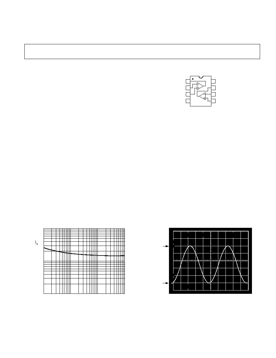
CONNECTION DIAGRAM
8-Lead Plastic DIP, MSOP, and SOIC
1
2
3
4
8
7
6
5
AD822
OUT1
≠IN1
+IN1
V≠
V+
OUT2
≠IN2
+IN2
a
Single Supply, Rail-to-Rail
Low Power FET-Input Op Amp
AD822
FEATURES
True Single Supply Operation
Output Swings Rail to Rail
Input Voltage Range Extends below Ground
Single Supply Capability from 3 V to 36 V
Dual Supply Capability from 1.5 V to 18 V
High Load Drive
Capacitive Load Drive of 350 pF, G = +1
Minimum Output Current of 15 mA
Excellent AC Performance for Low Power
800 mA Max Quiescent Current per Amplifier
Unity Gain Bandwidth: 1.8 MHz
Slew Rate of 3.0 V/ms
Good DC Performance
800 mV Max Input Offset Voltage
2 mV/ C Typ Offset Voltage Drift
25 pA Max Input Bias Current
Low Noise
13 nV/
Hz @ 10 kHz
No Phase Inversion
APPLICATIONS
Battery-Powered Precision Instrumentation
Photodiode Preamps
Active Filters
12- to 14-Bit Data Acquisition Systems
Medical Instrumentation
Low Power References and Regulators
PRODUCT DESCRIPTION
The AD822 is a dual precision, low power FET input op amp
that can operate from a single supply of 3.0 V to 36 V, or dual
supplies of
±1.5 V to ±18 V. It has true single supply capability
with an input voltage range extending below the negative rail,
allowing the AD822 to accommodate input signals below ground
in the single supply mode. Output voltage swing extends to
within 10 mV of each rail providing the maximum output
dynamic range.
Offset voltage of 800
µV max, offset voltage drift of 2 µV/∞C,
input bias currents below 25 pA and low input voltage noise
provide dc precision with source impedances up to a Gigaohm.
1.8 MHz unity gain bandwidth, ≠93 dB THD at 10 kHz and
3 V/
µs slew rate are provided with a low supply current of 800 µA
per amplifier. The AD822 drives up to 350 pF of direct capacitive
load as a follower, and provides a minimum output current of
15 mA. This allows the amplifier to handle a wide range of load
conditions. This combination of ac and dc performance, plus
the outstanding load drive capability, results in an exceptionally
versatile amplifier for the single supply user.
The AD822 is available in two performance grades. The A and
B grades are rated over the industrial temperature range of ≠40
∞C
to +85
∞C.
The AD822 is offered in three varieties of 8-lead package:
Plastic DIP, MSOP, and SOIC.
20 s
1V
90
100
10
0%
.
.
.
.
.
.
.
.
.
.
.
.
. .
.
.
. .
.
.
. .
.
.
. .
.
.
. .
.
.
. .
.
.
. .
.
.
.
.
.
.
.
.
.
.
.
.
.
.
. .
.
.
. .
.
.
. .
.
.
. .
.
.
. .
.
.
. .
.
.
. .
.
.
.
1V
1V
(GND)
V
OUT
5V
0V
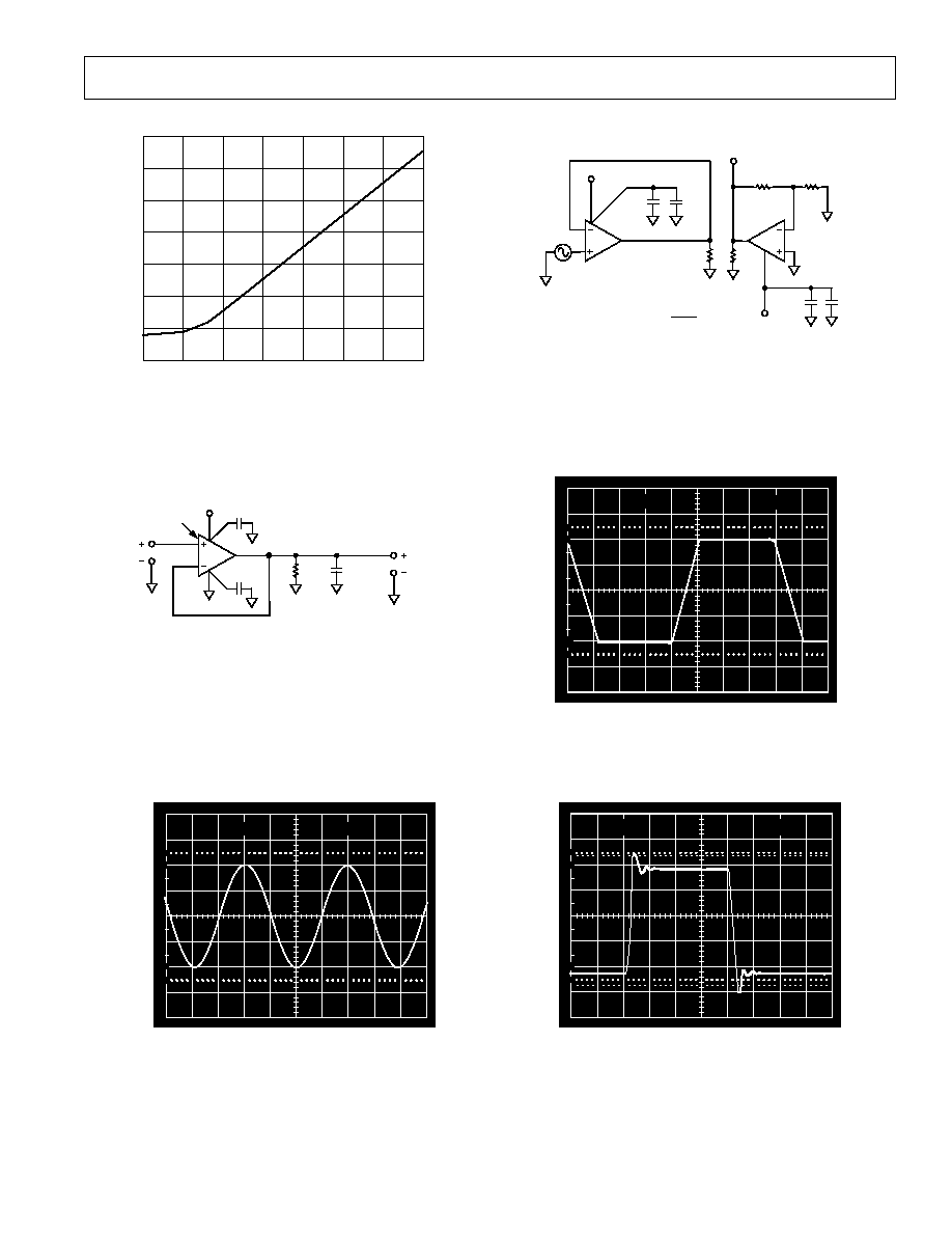
Figure 2. Gain-of-2 Amplifier; V
S
= 5, 0, V
IN
= 2.5 V Sine
Centered at 1.25 V, R
L
= 100 k
FREQUENCY ≠ Hz
1
10
10k
1k
100
INPUT
VOLTAGE
NOISE
≠
nV/
H
Z
100
10
Figure 1. Input Voltage Noise vs. Frequency
REV. B
Information furnished by Analog Devices is believed to be accurate and
reliable. However, no responsibility is assumed by Analog Devices for its
use, nor for any infringements of patents or other rights of third parties
which may result from its use. No license is granted by implication or
otherwise under any patent or patent rights of Analog Devices.
One Technology Way, P.O. Box 9106, Norwood, MA 02062-9106, U.S.A.
Tel: 781/329-4700
www.analog.com
Fax: 781/326-8703
© Analog Devices, Inc., 2001

REV. B
≠2≠
AD822≠SPECIFICATIONS
(V
S
= 0, 5 V @ T
A
= 25 C, V
CM
= 0 V, V
OUT
= 0.2 V unless otherwise noted.)
AD822A
AD822B
Parameter
Conditions
Min
Typ
Max
Min
Typ
Max
Unit
DC PERFORMANCE
Initial Offset
0.1
0.8
0.1
0.4
mV
Max Offset over Temperature
0.5
1.2
0.5
0.9
mV
Offset Drift
2
2
µV/∞C
Input Bias Current
V
CM
= 0 V to 4 V
2
25
2
10
pA
at T
MAX
0.5
5
0.5
2.5
nA
Input Offset Current
2
20
2
10
pA
at T
MAX
0.5
0.5
nA
Open-Loop Gain
V
O
= 0.2 V to 4 V
R
L
= 100 k
500
1000
500
1000
V/mV
T
MIN
to T
MAX
400
400
V/mV
R
L
= 10 k
80
150
80
150
V/mV
T
MIN
to T
MAX
80
80
V/mV
R
L
= 1 k
15
30
15
30
V/mV
T
MIN
to T
MAX
10
10
V/mV
NOISE/HARMONIC PERFORMANCE
Input Voltage Noise
0.1 Hz to 10 Hz
2
2
µV p-p
f = 10 Hz
25
25
nV/
Hz
f = 100 Hz
21
21
nV/
Hz
f = 1 kHz
16
16
nV/
Hz
f = 10 kHz
13
13
nV/
Hz
Input Current Noise
0.1 Hz to 10 Hz
18
18
fA p-p
f = 1 kHz
0.8
0.8
fA/
Hz
Harmonic Distortion
R
L
= 10 k
to 2.5 V
f = 10 kHz
V
O
= 0.25 V to 4.75 V
≠93
≠93
dB
DYNAMIC PERFORMANCE
Unity Gain Frequency
1.8
1.8
MHz
Full Power Response
V
O
p-p = 4.5 V
210
210
kHz
Slew Rate
3
3
V/
µs
Settling Time
to 0.1%
V
O
= 0.2 V to 4.5 V
1.4
1.4
µs
to 0.01%
1.8
1.8
µs
MATCHING CHARACTERISTICS
Initial Offset
1.0
0.5
mV
Max Offset over Temperature
1.6
1.3
mV
Offset Drift
3
3
µV/∞C
Input Bias Current
20
10
pA
Crosstalk @ f = 1 kHz
R
L
= 5 k
≠130
≠130
dB
f = 100 kHz
≠93
≠93
dB
INPUT CHARACTERISTICS
Common-Mode Voltage Range
2
≠0.2
+4
≠0.2
+4
V
T
MIN
to T
MAX
≠0.2
+4
≠0.2
+4
V
CMRR
V
CM
= 0 V to 2 V
66
80
69
80
dB
T
MIN
to T
MAX
66
66
dB
Input Impedance
Differential
10
13
0.5
10
13
0.5
pF
Common Mode
10
13
2.8
10
13
2.8
pF
OUTPUT CHARACTERISTICS
Output Saturation Voltage
3
V
OL
≠V
EE
I
SINK
= 20
µA
5
7
5
7
mV
T
MIN
to T
MAX
10
10
mV
V
CC
≠V
OH
I
SOURCE
= 20
µA
10
14
10
14
mV
T
MIN
to T
MAX
20
20
mV
V
OL
≠V
EE
I
SINK
= 2 mA
40
55
40
55
mV
T
MIN
to T
MAX
80
80
mV
V
CC
≠V
OH
I
SOURCE
= 2 mA
80
110
80
110
mV
T
MIN
to T
MAX
160
160
mV
V
OL
≠V
EE
I
SINK
= 15 mA
300
500
300
500
mV
T
MIN
to T
MAX
1000
1000
mV
V
CC
≠V
OH
I
SOURCE
= 15 mA
800
1500
800
1500
mV
T
MIN
to T
MAX
1900
1900
mV
Operating Output Current
15
15
mA
T
MIN
to T
MAX
12
12
mA
Capacitive Load Drive
350
350
pF
POWER SUPPLY
Quiescent Current T
MIN
to T
MAX
1.24
1.6
1.24
1.6
mA
Power Supply Rejection
V
S
+ = 5 V to 15 V
66
80
70
80
dB
T
MIN
to T
MAX
66
70
dB

(V
S
= 5 V @ T
A
= 25 C, V
CM
= 0 V, V
OUT
= 0 V unless otherwise noted.)
AD822A
AD822B
Parameter
Conditions
Min
Typ
Max
Min
Typ
Max
Unit
DC PERFORMANCE
Initial Offset
0.1
0.8
0.1
0.4
mV
Max Offset over Temperature
0.5
1.5
0.5
1
mV
Offset Drift
2
2
µV/∞C
Input Bias Current
V
CM
= ≠5 V to +4 V
2
25
2
10
pA
at T
MAX
0.5
5
0.5
2.5
nA
Input Offset Current
2
20
2
10
pA
at T
MAX
0.5
0.5
nA
Open-Loop Gain
V
O
= ≠4 V to +4 V
R
L
= 100 k
400
1000
400
1000
V/mV
T
MIN
to T
MAX
400
400
V/mV
R
L
= 10 k
80
150
80
150
V/mV
T
MIN
to T
MAX
80
80
V/mV
R
L
= 1 k
20
30
20
30
V/mV
T
MIN
to T
MAX
10
10
V/mV
NOISE/HARMONIC PERFORMANCE
Input Voltage Noise
0.1 Hz to 10 Hz
2
2
µV p-p
f = 10 Hz
25
25
nV/
Hz
f = 100 Hz
21
21
nV/
Hz
f = 1 kHz
16
16
nV/
Hz
f = 10 kHz
13
13
nV/
Hz
Input Current Noise
0.1 Hz to 10 Hz
18
18
fA p-p
f = 1 kHz
0.8
0.8
fA/
Hz
Harmonic Distortion
R
L
= 10 k
f = 10 kHz
V
O
=
±4.5 V
≠93
≠93
dB
DYNAMIC PERFORMANCE
Unity Gain Frequency
1.9
1.9
MHz
Full Power Response
V
O
p-p = 9 V
105
105
kHz
Slew Rate
3
3
V/
µs
Settling Time
to 0.1%
V
O
= 0 V to
±4.5 V
1.4
1.4
µs
to 0.01%
1.8
1.8
µs
MATCHING CHARACTERISTICS
Initial Offset
1.0
0.5
mV
Max Offset over Temperature
3
2
mV
Offset Drift
3
3
µV/∞C
Input Bias Current
25
10
pA
Crosstalk @ f = 1 kHz
R
L
= 5 k
≠130
≠130
dB
f = 100 kHz
≠93
≠93
dB
INPUT CHARACTERISTICS
Common-Mode Voltage Range
2
≠5.2
+4
≠5.2
+4
V
T
MIN
to T
MAX
≠5.2
+4
≠5.2
+4
V
CMRR
V
CM
= ≠5 V to +2 V
66
80
69
80
dB
T
MIN
to T
MAX
66
66
dB
Input Impedance
Differential
10
13
0.5
10
13
0.5
pF
Common Mode
10
13
2.8
10
13
2.8
pF
OUTPUT CHARACTERISTICS
Output Saturation Voltage
3
V
OL
≠V
EE
I
SINK
= 20
µA
5
7
5
7
mV
T
MIN
to T
MAX
10
10
mV
V
CC
≠V
OH
I
SOURCE
= 20
µA
10
14
10
14
mV
T
MIN
to T
MAX
20
20
mV
V
OL
≠V
EE
I
SINK
= 2 mA
40
55
40
55
mV
T
MIN
to T
MAX
80
80
mV
V
CC
≠V
OH
I
SOURCE
= 2 mA
80
110
80
110
mV
T
MIN
to T
MAX
160
160
mV
V
OL
≠V
EE
I
SINK
= 15 mA
300
500
300
500
mV
T
MIN
to T
MAX
1000
1000
mV
V
CC
≠V
OH
I
SOURCE
= 15 mA
800
1500
800
1500
mV
T
MIN
to T
MAX
1900
1900
mV
Operating Output Current
15
15
mA
T
MIN
to T
MAX
12
12
mA
Capacitive Load Drive
350
350
pF
POWER SUPPLY
Quiescent Current T
MIN
to T
MAX
1.3
1.6
1.3
1.6
mA
Power Supply Rejection
V
S
+ = 5 V to 15 V
66
80
70
80
dB
T
MIN
to T
MAX
66
70
dB
AD822
REV. B
≠3≠

AD822A
AD822B
Parameter
Conditions
Min
Typ
Max
Min
Typ
Max
Unit
DC PERFORMANCE
Initial Offset
0.4
2
0.3
1.5
mV
Max Offset over Temperature
0.5
3
0.5
2.5
mV
Offset Drift
2
2
µV/∞C
Input Bias Current
V
CM
= 0 V
2
25
2
12
pA
V
CM
= ≠10 V
40
40
pA
at T
MAX
V
CM
= 0 V
0.5
5
0.5
2.5
nA
Input Offset Current
2
20
2
12
pA
at T
MAX
0.5
0.5
nA
Open-Loop Gain
V
O
= +10 V to ≠10 V
R
L
= 100 k
500
2000
500
2000
V/mV
T
MIN
to T
MAX
500
500
V/mV
R
L
= 10 k
100
500
100
500
V/mV
T
MIN
to T
MAX
100
100
V/mV
R
L
= 1 k
30
45
30
45
V/mV
T
MIN
to T
MAX
20
20
V/mV
NOISE/HARMONIC PERFORMANCE
Input Voltage Noise
0.1 Hz to 10 Hz
2
2
µV p-p
f = 10 Hz
25
25
nV/
Hz
f = 100 Hz
21
21
nV/
Hz
f = 1 kHz
16
16
nV/
Hz
f = 10 kHz
13
13
nV/
Hz
Input Current Noise
0.1 Hz to 10 Hz
18
18
fA p-p
f = 1 kHz
0.8
0.8
fA/
Hz
Harmonic Distortion
R
L
= 10 k
f = 10 kHz
V
O
=
±10 V
≠85
≠85
dB
DYNAMIC PERFORMANCE
Unity Gain Frequency
1.9
1.9
MHz
Full Power Response
V
O
p-p = 20 V
45
45
kHz
Slew Rate
3
3
V/
µs
Settling Time
to 0.1%
V
O
= 0 V to
±10 V
4.1
4.1
µs
to 0.01%
4.5
4.5
µs
MATCHING CHARACTERISTICS
Initial Offset
3
2
mV
Max Offset over Temperature
4
2.5
mV
Offset Drift
3
3
µV/∞C
Input Bias Current
25
12
pA
Crosstalk @ f = 1 kHz
R
L
= 5 k
≠130
≠130
dB
f = 100 kHz
≠93
≠93
dB
INPUT CHARACTERISTICS
Common-Mode Voltage Range
2
≠15.2
+14
≠15.2
+14
V
T
MIN
to T
MAX
≠15.2
+14
≠15.2
+14
V
CMRR
V
CM
= ≠15 V to +12 V
70
80
74
90
dB
T
MIN
to T
MAX
70
74
dB
Input Impedance
Differential
10
13
0.5
10
13
0.5
pF
Common Mode
10
13
2.8
10
13
2.8
pF
OUTPUT CHARACTERISTICS
Output Saturation Voltage
3
V
OL
≠V
EE
I
SINK
= 20
µA
5
7
5
7
mV
T
MIN
to T
MAX
10
10
mV
V
CC
≠V
OH
I
SOURCE
= 20
µA
10
14
10
14
mV
T
MIN
to T
MAX
20
20
mV
V
OL
≠V
EE
I
SINK
= 2 mA
40
55
40
55
mV
T
MIN
to T
MAX
80
80
mV
V
CC
≠V
OH
I
SOURCE
= 2 mA
80
110
80
110
mV
T
MIN
to T
MAX
160
160
mV
V
OL
≠V
EE
I
SINK
= 15 mA
300
500
300
500
mV
T
MIN
to T
MAX
1000
1000
mV
V
CC
≠V
OH
I
SOURCE
= 15 mA
800
1500
800
1500
mV
T
MIN
to T
MAX
1900
1900
mV
Operating Output Current
20
20
mA
T
MIN
to T
MAX
15
15
mA
Capacitive Load Drive
350
350
pF
POWER SUPPLY
Quiescent Current T
MIN
to T
MAX
1.4
1.8
1.4
1.8
mA
Power Supply Rejection
V
S
+ = 5 V to 15 V
70
80
70
80
dB
T
MIN
to T
MAX
70
70
dB
AD822≠SPECIFICATIONS
(V
S
= 15 V @ T
A
= 25 C, V
CM
= 0 V, V
OUT
= 0 V unless otherwise noted.)
REV. B
≠4≠

AD822
REV. B
(V
S
= 0, 3 V @ T
A
= 25 C, V
CM
= 0 V, V
OUT
= 0.2 V unless otherwise noted.)
Parameter
Conditions
Typ
Unit
DC PERFORMANCE
Initial Offset
0.2
mV
Max Offset over Temperature
0.5
mV
Offset Drift
1
µV/∞C
Input Bias Current
V
CM
= 0 V to 2 V
2
pA
at T
MAX
0.5
nA
Input Offset Current
2
pA
at T
MAX
0.5
nA
Open-Loop Gain
V
O
= 0.2 V to 2 V
R
L
= 100 k
1000
V/mV
T
MIN
to T
MAX
R
L
= 10 k
150
V/mV
T
MIN
to T
MAX
R
L
= 1 k
30
V/mV
T
MIN
to T
MAX
NOISE/HARMONIC PERFORMANCE
Input Voltage Noise
0.1 Hz to 10 Hz
2
µV p-p
f = 10 Hz
25
nV/
Hz
f = 100 Hz
21
nV/
Hz
f = 1 kHz
16
nV/
Hz
f = 10 kHz
13
nV/
Hz
Input Current Noise
0.1 Hz to 10 Hz
18
fA p-p
f = 1 kHz
0.8
fA/
Hz
Harmonic Distortion
R
L
= 10 k
to 1.5 V
f = 10 kHz
V
O
=
±1.25 V
≠92
dB
DYNAMIC PERFORMANCE
Unity Gain Frequency
1.5
MHz
Full Power Response
V
O
p-p = 2.5 V
240
kHz
Slew Rate
3
V/
µs
Settling Time
to 0.1%
V
O
= 0.2 V to 2.5 V
1
µs
to 0.01%
1.4
µs
MATCHING CHARACTERISTICS
Initial Offset
Max Offset over Temperature
Offset Drift
2
µV/∞C
Input Bias Current
Crosstalk @ f = 1 kHz
R
L
= 5 k
≠130
dB
f = 100 kHz
≠93
dB
INPUT CHARACTERISTICS
Common-Mode Voltage Range
2
T
MIN
to T
MAX
CMRR
V
CM
= 0 V to 1 V
74
dB
T
MIN
to T
MAX
Input Impedance
Differential
10
13
0.5
pF
Common Mode
10
13
2.8
pF
OUTPUT CHARACTERISTICS
Output Saturation Voltage
3
V
OL
≠V
EE
I
SINK
= 20
µA
5
mV
T
MIN
to T
MAX
V
CC
≠V
OH
I
SOURCE
= 20
µA
10
mV
T
MIN
to T
MAX
V
OL
≠V
EE
I
SINK
= 2 mA
40
mV
T
MIN
to T
MAX
V
CC
≠V
OH
I
SOURCE
= 2 mA
80
mV
T
MIN
to T
MAX
V
OL
≠V
EE
I
SINK
= 10 mA
200
mV
T
MIN
to T
MAX
V
CC
≠V
OH
I
SOURCE
= 10 mA
500
mV
T
MIN
to T
MAX
Operating Output Current
T
MIN
to T
MAX
Capacitive Load Drive
350
pF
POWER SUPPLY
Quiescent Current T
MIN
to T
MAX
1.24
mA
Power Supply Rejection
V
S
+ = 3 V to 15 V
80
dB
T
MIN
to T
MAX
≠5≠
≠6≠
AD822
REV. B
NOTES
1
See standard military drawing for 883B specifications.
2
This is a functional specification. Amplifier bandwidth decreases when the input common-mode voltage is driven in the range (+V
S
≠ 1 V) to +V
S
.
Common-mode error voltage is typically less than 5 mV with the common-mode voltage set at 1 volt below the positive supply.
3
V
OL
≠V
EE
is defined as the difference between the lowest possible output voltage (V
OL
) and the minus voltage supply rail (V
EE
).
V
CC
≠V
OH
is defined as the difference between the highest possible output voltage (V
OH
) and the positive supply voltage (V
CC
).
Specifications subject to change without notice.
ABSOLUTE MAXIMUM RATINGS
1
Supply Voltage . . . . . . . . . . . . . . . . . . . . . . . . . . . . . . .
±18 V
Internal Power Dissipation
Plastic DIP (N) . . . . . . . . . . . . . . Observe Derating Curves
SOIC (R) . . . . . . . . . . . . . . . . . . . Observe Derating Curves
Input Voltage . . . . . . . . . . . . . . (+V
S
+ 0.2 V) to ≠(20 V + V
S
)
Output Short Circuit Duration . . . . . . . . . . . . . . . . Indefinite
Differential Input Voltage . . . . . . . . . . . . . . . . . . . . . .
±30 V
Storage Temperature Range (N) . . . . . . . . . ≠65
∞C to +125∞C
Storage Temperature Range (R, RM) . . . . . ≠65
∞C to +150∞C
Operating Temperature Range
AD822A/B . . . . . . . . . . . . . . . . . . . . . . . . ≠40
∞C to +85∞C
Lead Temperature Range (Soldering 60 sec) . . . . . . . . 260
∞C
NOTES
1
Stresses above those listed under Absolute Maximum Ratings may cause perma-
nent damage to the device. This is a stress rating only; functional operation of the
device at these or any other conditions above those indicated in the operational
section of this specification is not implied. Exposure to absolute maximum rating
conditions for extended periods may affect device reliability.
2
8-Lead Plastic DIP Package:
JA
= 90
∞C/W
8-Lead SOIC Package:
JA
= 160
∞C/W
8-Lead MSOP Package:
JA
= 190
∞C/W
MAXIMUM POWER DISSIPATION
The maximum power that can be safely dissipated by the AD822
is limited by the associated rise in junction temperature. For plastic
packages, the maximum safe junction temperature is 145
∞C. If
these maximums are exceeded momentarily, proper circuit
operation will be restored as soon as the die temperature is
reduced. Leaving the device in the "overheated" condition for
an extended period can result in device burnout. To ensure
proper operation, it is important to observe the derating curves
shown in TPC 24.
While the AD822 is internally short circuit protected, this may not
be sufficient to guarantee that the maximum junction temperature
is not exceeded under all conditions. With power supplies
±12 V
(or less) at an ambient temperature of 25
∞C or less, if the output
node is shorted to a supply rail, then the amplifier will not be
destroyed, even if this condition persists for an extended period.
AD822≠SPECIFICATIONS
CAUTION
ESD (electrostatic discharge) sensitive device. Electrostatic charges as high as 4000 V readily
accumulate on the human body and test equipment and can discharge without detection. Although
the AD822 features proprietary ESD protection circuitry, permanent damage may occur on devices
subjected to high-energy electrostatic discharges. Therefore, proper ESD precautions are
recommended to avoid performance degradation or loss of functionality.
WARNING!
ESD SENSITIVE DEVICE
ORDERING GUIDE
Package
Branding
M
odel
*
Temperature Range
Package Description
Option
Information
AD822AN
≠40
∞C to +85∞C
8-Lead PDIP
N-8
AD822AR
≠40
∞C to +85∞C
8-Lead SOIC
R-8
AD822ARM
≠40
∞C to +85∞C
8-Lead Mini_SOIC
RM-8
B4A
AD822BR
≠40
∞C to +85∞C
8-Lead SOIC
R-8
*SPICE model is available at www.analog.com.
Typical Performance Characteristics≠AD822
REV. B
≠7≠
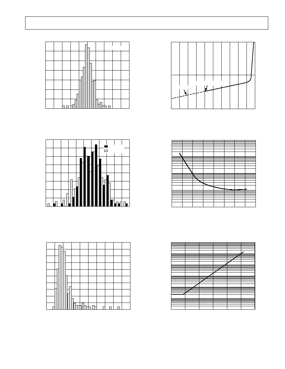
OFFSET VOLTAGE ≠ mV
70
0
≠0.5
≠0.4
NUMBER OF UNITS
≠0.3 ≠0.2
≠0.1
0
60
50
40
30
20
10
0.1
0.2
0.3
0.4
0.5
V
S
= 0V, 5V
TPC 1. Typical Distribution of Offset Voltage (390 Units)
V
S
=
5V
V
S
=
15V
OFFSET VOLTAGE DRIFT ≠ V/ C
16
6
0
≠12
10
≠10
% IN BIN
≠8
≠6
≠4
≠2
0
2
4
6
8
14
8
4
2
12
10
TPC 2. Typical Distribution of Offset Voltage Drift
(100 Units)
INPUT BIAS CURRENT ≠ pA
50
20
0
0
10
1
NUMBER OF UNITS
2
3
4
5
6
7
8
9
45
25
15
5
35
30
10
40
TPC 3. Typical Distribution of Input Bias Current
(213 Units)
COMMON-MODE VOLTAGE ≠ V
5
0
≠5
≠5
5
≠4
INPUT BIAS CURRENT
≠
pA
≠3
≠2
≠1
0
1
2
3
4
V
S
= 0V, +5V AND 5V
V
S
= 5V
TPC 4. Input Bias Current vs. Common-Mode Voltage;
V
S
= 5 V, 0 V and V
S
=
±5 V
COMMON-MODE VOLTAGE ≠ V
1k
100
0.1
≠16
16
≠12
INPUT BIAS CURRENT
≠
pA
≠8
≠4
0
4
8
12
10
1
TPC 5. Input Bias Current vs. Common-Mode Voltage;
V
S
=
±15 V
TEMPERATURE ≠
C
100k
0.1
20
140
40
INPUT BIAS CURRENT
≠
pA
60
80
100
120
10k
1k
100
10
1
TPC 6. Input Bias Current vs. Temperature; V
S
= 5 V,
V
CM
= 0
≠8≠
AD822
REV. B
LOAD RESISTANCE ≠
10M
1M
10k
100
100k
0PEN-LOOP
GAIN
≠
V/V
100k
V
S
= 0V. 3V
V
S
=
15V
V
S
= 0V, 5V
1k
10k
TPC 7. Open-Loop Gain vs. Load Resistance
TEMPERATURE ≠ C
10M
1M
10k
≠60
140
≠40
OPEN-LOOP
GAIN
≠
V/V
≠20
0
20
40
60
80
100
120
100k
R
L
= 10k
R
L
= 100k
R
L
= 600
V
S
= 15V
V
S
= 15V
V
S
= 15V
V
S
= 0V, 5V
V
S
= 0V, 5V
V
S
= 0V, 5V
TPC 8. Open-Loop Gain vs. Temperature
OUTPUT VOLTAGE ≠ V
300
≠300
≠16
16
≠12
INPUT VOL
T
AGE
≠
V
≠8
≠4
0
4
8
12
200
100
0
≠100
≠200
R
L
= 10k
R
L
= 600
R
L
= 100k
TPC 9. Input Error Voltage vs. Output Voltage for
Resistive Loads
OUTPUT VOLTAGE FROM SUPPLY RAILS ≠ mV
40
20
≠40
0
300
60
INPUT VOL
T
AGE
≠
V
120
180
240
0
≠20
R
L
= 2k
R
L
= 20k
POS RAIL
NEG RAIL
NEG RAIL
NEG RAIL
POS RAIL
POS
RAIL
R
L
= 100k
TPC 10. Input Error Voltage with Output Voltage within
300 mV of Either Supply Rail for Various Resistive Loads;
V
S
=
±5 V
FREQUENCY ≠ Hz
1k
100
1
1
10k
10
100
1k
10
INPUT
VOLTAGE
NOISE
≠
nV/
H
Z
TPC 11. Input Voltage Noise vs. Frequency
FREQUENCY ≠ Hz
≠40
≠50
≠110
100
100k
1k
THD
≠
dB
10k
≠70
≠80
≠90
≠100
≠60
R
L
= 10k
A
CL
= ≠1
V
S
= 0V, 5V; V
OUT
= 4.5V p-p
V
S
= 5V; V
OUT
= 9V p-p
V
S
= 15V; V
OUT
= 20V p-p
V
S
= 0V, 3V; V
OUT
= 2.5V p-p
TPC 12. Total Harmonic Distortion vs. Frequency
AD822
REV. B
≠9≠
FREQUENCY ≠ Hz
100
≠20
80
60
40
20
0
10
10M
100
OPEN-LOOP
GAIN
≠
dB
1k
10k
100k
1M
100
≠20
80
60
40
20
0
PHASE MARGIN IN DEGREES
PHASE
GAIN
C
L
= 100pF
R
L
= 2k
TPC 13. Open-Loop Gain and Phase Margin vs.
Frequency
FREQUENCY ≠ Hz
1k
100
100
10M
1k
OUTPUT IMPEDANCE
≠
10k
100k
1M
10
1
A
CL
= +1
V
S
= 15V
0.1
0.01
TPC 14. Output Impedance vs. Frequency
SETTLING TIME ≠
s
16
12
≠16
0.0
5.0
1.0
OUTPUT SWING FROM 0 T
O
VOL
T
S
2.0
3.0
4.0
0
≠4
≠8
≠12
8
4
1%
0.01%
1%
0.01%
0.1%
ERROR
TPC 15. Output Swing and Error vs. Settling Time
90
80
0
40
30
20
10
60
50
70
COMMON-MODE REJECTION
≠
dB
FREQUENCY ≠ Hz
10M
100
1k
10k
100k
1M
10
V
S
=
15V
V
S
= 0V, 3V
V
S
= 0V, 5V
TPC 16. Common-Mode Rejection vs. Frequency
+125 C
≠55 C
+25 C
POSITIVE
RAIL
NEGATIVE
RAIL
COMMON-MODE VOLTAGE FROM SUPPLY RAILS ≠ V
5
4
0
≠1
3
COMMON-MODE ERROR VOL
T
AGE
≠
mV
0
1
2
3
2
1
≠55 C
+125 C
TPC 17. Absolute Common-Mode Error vs. Common-
Mode Voltage from Supply Rails (V
S
≠ V
CM
)
LOAD CURRENT ≠ mA
1000
100
0
0.001
100
0.01
OUTPUT SA
TURA
TION VOL
T
AGE
≠
mV
0.1
1
10
10
V
OL
≠ V
S
V
S
≠ V
OH
TPC 18. Output Saturation Voltage vs. Load Current
≠10≠
AD822
REV. B
TEMPERATURE ≠ C
1000
100
1
≠60
140
≠40
OUTPUT SA
TURA
TION VOL
T
AGE
≠
mV
≠20
0
20
40
60
80
100
120
10
I
SOURCE
= 10mA
I
SINK
= 10mA
I
SOURCE
= 1mA
I
SINK
= 1mA
I
SOURCE
= 10 A
I
SINK
= 10 A
TPC 19. Output Saturation Voltage vs. Temperature
TEMPERATURE ≠ C
80
40
0
≠60
140
≠40
≠20
0
20
40
60
80
100
120
SHORT CIRCUIT CURRENT LIMIT
≠
mA
70
60
20
10
50
30
+
≠
≠
+
+
V
S
= 15V
V
S
= 15V
V
S
= 0V, 5V
V
S
= 0V, 3V
V
S
= 0V, 3V
V
S
= 0V, 5V
≠OUT
TPC 20. Short Circuit Current Limit vs. Temperature
TOTAL SUPPLY VOLTAGE ≠ V
1600
0
0
36
4
QUIESCENT CURRENT
≠
A
8
12
16
20
24
28
32
1400
800
600
400
200
1200
1000
T = +125 C
T = +25 C
T = ≠55 C
TPC 21. Quiescent Current vs. Supply Voltage vs.
Temperature
FREQUENCY ≠ Hz
100
0
10
10M
100
POWER SUPPL
Y
REJECTION
≠
dB
1k
10k
100k
1M
90
60
30
20
10
80
70
50
40
≠PSRR
+PSRR
TPC 22. Power Supply Rejection vs. Frequency
FREQUENCY ≠ Hz
30
25
0
10k
10M
100k
OUTPUT VOL
T
AGE
≠
V
1M
20
15
10
5
V
S
= 15V
R
L
= 2k
V
S
= 0V, 3V
V
S
= 0V, 5V
TPC 23. Large Signal Frequency Response
AMBIENT TEMPERATURE ≠ C
2.4
1.2
0.4
≠60
≠40
T
O
T
A
L
POWER DISSIP
A
TION
≠
Watts
≠20
0
20
40
60
80
2.2
1.4
1.0
0.6
1.8
1.6
0.8
2.0
0.2
0.0
8-LEAD MINI-DIP
8-LEAD SOIC
8-LEAD MSOP
TPC 24. Maximum Power Dissipation vs. Temperature for
Plastic Packages
AD822
REV. B
≠11≠
TPC 25. Crosstalk vs. Frequency
1/2
AD822
8
4
V
IN
+V
S
R
L
0.01 F
V
OUT
0.01 F
100pF
TPC 26. Unity-Gain Follower
0%
100
90
10 s
5V
10
TPC 27. 20 V p-p, 25 kHz Sine Wave Input; Unity Gain
Follower; R
L
= 600
, V
S
=
±1 5 V
0.1 F
1 F
0.1 F
1 F
+V
S
1/2
AD822
1/2
AD822
20V p-p
2
3
8
1
7
5
6
20k
2.2k
5k
5k
≠V
S
V
OUT
V
IN
CROSSTALK = 20LOG
V
OUT
10V
IN
TPC 28. Crosstalk Test Circuit
0%
100
90
10
5 s
5V
TPC 29. Large Signal Response Unity Gain Follower;
V
S
=
±15 V, R
L
= 10 k
10
0%
100
90
500ns
10mV
TPC 30. Small Signal Response Unity Gain Follower;
V
S
=
±15 V, R
L
= 10 k
FREQUENCY ≠ Hz
≠70
≠140
300
1M
1k
CROSST
ALK
≠
dB
3k
10k
30k
100k
300k
≠80
≠100
≠110
≠120
≠130
≠90
≠12≠
AD822
REV. B
10
0%
100
90
GND
2 s
1V
TPC 31. V
S
= 5 V, 0 V; Unity Gain Follower Response
to 0 V to 4 V Step
1/2
AD822
8
4
V
IN
+V
S
R
L
0.01 F
V
OUT
100pF
TPC 32. Unity Gain Follower
0.01 F
V
OUT
+V
S
1/2
AD822
8
20k
V
IN
10k
4
R
L
100pF
TPC 33. Gain-of-Two Inverter
10
0%
100
90
1V
2 s
GND
TPC 34. V
S
= 5 V, 0 V; Unity Gain Follower Response
to 0 V to 5 V Step
10
0%
100
90
GND
10mV
2 s
TPC 35. V
S
= 5 V, 0 V; Unity Gain Follower Response, to
40 mV Step Centered 40 mV Above Ground, R
L
= 10 k
10
0%
100
90
GND
10mV
2 s
TPC 36. V
S
= 5 V, 0 V; Gain-of-Two Inverter Response to
20 mV Step, Centered 20 mV Below Ground, R
L
= 10 k
AD822
REV. B
≠13≠
10
0%
100
90
1V
GND
2 s
TPC 37. V
S
= 5 V, 0 V; Gain-of-Two Inverter Response to
2.5 V Step Centered ≠1.25 V Below Ground, R
L
= 10 k
10
0%
100
90
GND
500mV
10 s
TPC 38. V
S
= 3 V, 0 V; Gain-of-Two Inverter, V
IN
= 1.25 V,
25 kHz, Sine Wave Centered at ≠0.75 V, R
L
= 600
10 s
1V
90
100
10
0%
.
.
.
.
.
.
.
.
.
.
.
.
. .
.
.
. .
.
.
. .
.
.
. .
.
.
. .
.
.
. .
.
.
. .
.
.
.
.
.
.
.
.
.
.
.
.
.
.
. .
.
.
. .
.
.
. .
.
.
. .
.
.
. .
.
.
. .
.
.
. .
.
.
.
1V
1V
(b)
GND
90
100
10
0%
.
.
.
.
.
.
.
.
.
.
.
.
. .
.
.
. .
.
.
. .
.
.
. .
.
.
. .
.
.
. .
.
.
. .
.
.
.
.
.
.
.
.
.
.
.
.
.
.
. .
.
.
. .
.
.
. .
.
.
. .
.
.
. .
.
.
. .
.
.
. .
.
.
.
10 s
1V
1V
(a)
GND
V
IN
V
OUT
5V
R
P
+V
S
TPC 39. (a) Response with R
P
= 0; V
IN
from 0 to +V
S
(b) V
IN
= 0 to +V
S
+ 200 mV
V
OUT
= 0 to +V
S
R
P
= 49.9 k
≠14≠
AD822
REV. B
APPLICATION NOTES
INPUT CHARACTERISTICS
In the AD822, n-channel JFETs are used to provide a low offset,
low noise, high impedance input stage. Minimum input common-
mode voltage extends from 0.2 V below ≠V
S
to 1 V less than +V
S
.
Driving the input voltage closer to the positive rail will cause a
loss of amplifier bandwidth (as can be seen by comparing the
large signal responses shown in TPCs 31 and 34) and increased
common-mode voltage error as illustrated in TPC 17.
The AD822 does not exhibit phase reversal for input voltages
up to and including +V
S
. TPC 39a shows the response of an
AD822 voltage follower to a 0 V to 5 V (+V
S
) square wave
input. The input and output are superimposed. The output
tracks the input up to +V
S
without phase reversal. The reduced
bandwidth above a 4 V input causes the rounding of the output
wave form. For input voltages greater than +V
S
, a resistor in
series with the AD822's noninverting input will prevent phase
reversal, at the expense of greater input voltage noise. This is
illustrated in TPC 39b.
Since the input stage uses n-channel JFETs, input current
during normal operation is negative; the current flows out from
the input terminals. If the input voltage is driven more positive
than +V
S
≠ 0.4 V, the input current will reverse direction as
internal device junctions become forward biased. This is illus-
trated in TPC 4.
A current limiting resistor should be used in series with the
input of the AD822 if there is a possibility of the input voltage
exceeding the positive supply by more than 300 mV, or if an
input voltage will be applied to the AD822 when
±V
S
= 0. The
amplifier will be damaged if left in that condition for more than
10 seconds. A 1 k
resistor allows the amplifier to withstand up
to 10 V of continuous overvoltage, and increases the input
voltage noise by a negligible amount.
Input voltages less than ≠V
S
are a completely different story.
The amplifier can safely withstand input voltages 20 V below
the minus supply voltage as long as the total voltage from the
positive supply to the input terminal is less than 36 V. In addi-
tion, the input stage typically maintains picoamp level input
currents across that input voltage range.
The AD822 is designed for 13 nV/
Hz wideband input voltage
noise and maintains low noise performance to low frequencies
(refer to TPC 11). This noise performance, along with the
AD822's low input current and current noise means that the
AD822 contributes negligible noise for applications with source
resistances greater than 10 k
and signal bandwidths greater
than 1 kHz. This is illustrated in Figure 3.
100k
0.1
INPUT VOL
T
AGE NOISE
≠
V
10k
1k
100
10
1
WHENEVER
JOHNSON
NOISE
IS
GREATER
THAN
AMPLIFIER
NOISE,
AMPLIFIER
NOISE
CAN
BE
CONSIDERED
NEGLIGIBLE
FOR
APPLICATION.
1kHz
RESISTOR
JOHNSON
NOISE
AMPLIFIER-GENERATED
NOISE
10Hz
10k
100k
1M
10M
100M
1G
10G
SOURCE IMPEDANCE ≠
Figure 3. Total Noise vs. Source Impedance
OUTPUT CHARACTERISTICS
The AD822 s unique bipolar rail-to-rail output stage swings
within 5 mV of the minus supply and 10 mV of the positive
supply with no external resistive load. The AD822's approximate
output saturation resistance is 40
sourcing and 20 sinking.
This can be used to estimate output saturation voltage when
driving heavier current loads. For instance, when sourcing 5 mA,
the saturation voltage to the positive supply rail will be 200 mV,
when sinking 5 mA, the saturation voltage to the minus rail will
be 100 mV.
The amplifier's open-loop gain characteristic will change as a
function of resistive load, as shown in TPCs 7 through 10. For
load resistances over 20 k
, the AD822's input error voltage is
virtually unchanged until the output voltage is driven to 180 mV
of either supply.
If the AD822's output is overdriven so as to saturate either of
the output devices, the amplifier will recover within 2
µs of its
input returning to the amplifier's linear operating region.
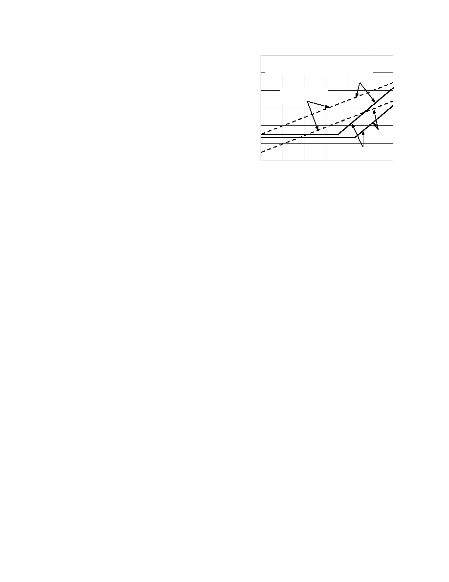
Direct capacitive loads will interact with the amplifier's effective
output impedance to form an additional pole in the amplifier's
feedback loop, which can cause excessive peaking on the pulse
response or loss of stability. Worst-case is when the amplifier is
used as a unity gain follower. Figure 4 shows the AD822's
pulse response as a unity gain follower driving 350 pF. This
amount of overshoot indicates approximately 20 degrees of phase
margin--the system is stable, but is nearing the edge. Configura-
tions with less loop gain, and as a result less loop bandwidth,
will be much less sensitive to capacitance load effects. Figure
5 is a plot of capacitive load that will result in a 20 degree phase
margin versus noise gain for the AD822. Noise gain is the inverse
of the feedback attenuation factor provided by the feedback
network in use.
AD822
REV. B
≠15≠
2 s
20mv
90
.
.
.
.
.
.
.
.
.
.
.
.
. .
.
.
. .
.
.
. .
.
.
. .
.
.
. .
.
.
. .
.
.
. .
.
.
.
.
.
.
.
.
.
.
.
.
.
.
. .
.
.
. .
.
.
. .
.
.
. .
.
.
. .
.
.
. .
.
.
. .
.
.
.
100
0%
10
Figure 4. Small Signal Response of AD822 as Unity Gain
Follower Driving 350 pF
1
2
3
4
5
300
1k
3k
10k
30k
CAPACITIVE
LOAD
FOR
20
O
PHASE
MARGIN
≠
pF
NOISE
GAIN
≠
1+
≠≠≠≠ R
1
R
F
R1
R
F
C
L
Figure 5. Capacitive Load Tolerance vs. Noise Gain
Figure 6 shows a method for extending capacitance load drive
capability for a unity gain follower. With these component val-
ues, the circuit will drive 5,000 pF with a 10% overshoot.
+V
S
V
OUT
V
IN
20pF
8
4
1/2
AD822
0.01 F
100
20k
0.01 F
C
L
≠V
S
Figure 6. Extending Unity Gain Follower Capacitive Load
Capability Beyond 350 pF
APPLICATIONS
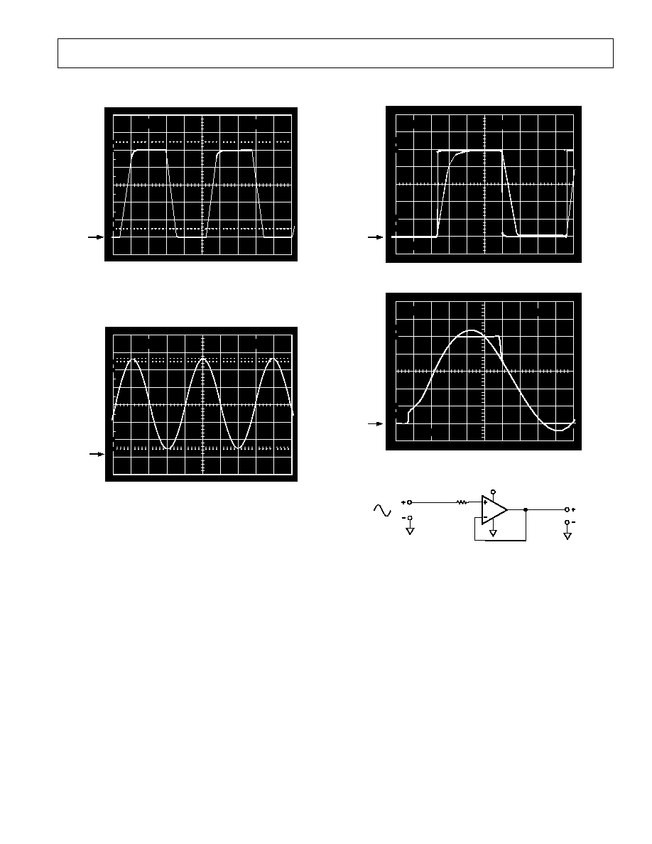
Single Supply Voltage-to-Frequency Converter
The circuit shown in Figure 7 uses the AD822 to drive a low
power timer, which produces a stable pulse of width t
1
. The
positive going output pulse is integrated by R1-C1 and used as
one input to the AD822, which is connected as a differential
integrator. The other input (nonloading) is the unknown voltage,
V
IN
. The AD822 output drives the timer trigger input, closing
the overall feedback loop.
NOTES:
f
OUT
= V
IN
/(V
REF
t
1
), t
1
= 1.1 R3 C6
+10V
C5
0.1 F
U4
REF-02
V
REF
= 5V
R
SCALE
**
10k
2
3
4
6
5
CMOS
74HCO4
U3A
U3B
C3
0.1 F
1
2
3
4
OUT2
OUT1
0.01 F, 2%
R2
499k 1%
U1
C1
R3*
116k
1/2
AD822B
U2
CMOS 555
THR
TR
DIS
GND
OUT
CV
R
V+
1
2
3
4
5
6
7
8
499k 1%
R1
V
IN
C2
0.01 F, 2%
0V TO 2.5V
FULL SCALE
C4
0.01 F
C6
390pF
5%
(NPO)
= 25kHz F
S
AS SHOWN
* = 1% METAL FILM, <50ppm/ C TC
** = 10% 20T FILM, <100ppm/ C TC
t
1
= 33 s FOR f
OUT
= 20kHz @ V
IN
= 2.0V
Figure 7. Single Supply Voltage-to-Frequency Converter
≠16≠
AD822
REV. B
Typical AD822 bias currents of 2 pA allow megohm-range
source impedances with negligible dc errors. Linearity errors on
the order of 0.01% full scale can be achieved with this circuit.
This performance is obtained with a 5 V single supply which
delivers less than 1 mA to the entire circuit.
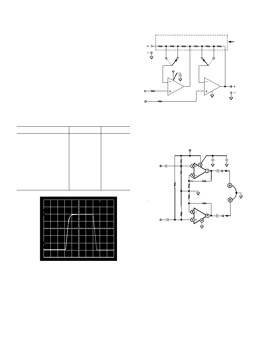
Single Supply Programmable Gain Instrumentation Amplifier
The AD822 can be configured as a single supply instrumenta-
tion amplifier that is able to operate from single supplies down to
3 V, or dual supplies up to
±15 V. Using only one AD822 rather
than three separate op amps, this circuit is cost and power effi-
cient. AD822 FET inputs' 2 pA bias currents minimize offset
errors caused by high unbalanced source impedances.
An array of precision thin-film resistors sets the in amp gain to
be either 10 or 100. These resistors are laser-trimmed to ratio
match to 0.01%, and have a maximum differential TC of
5 ppm/
∞C.
Table I. AD822 In Amp Performance
Parameters
V
S
= 3 V, 0 V
V
S
= 5 V
CMRR
74 dB
80 dB
Common-Mode
Voltage Range
≠0.2 V to +2 V
≠5.2 V to +4 V
3 dB BW, G = 10
180 kHz
180 kHz
G = 100
18 kHz
18 kHz
t
SETTLING
2 V Step (V
S
= 0 V, 3 V)
2
µs
5 V (V
S
=
±5 V)
5
µs
Noise @ f = 1 kHz, G = 10
270 nV/
Hz
270 nV/
Hz
G = 100
2.2
µV/Hz
2.2
µV/Hz
I
SUPPLY
(Total)
1.10 mA
1.15 mA
5 s
1V
90
100
10
0%
.
.
.
.
.
.
.
.
.
.
.
.
. .
.
.
. .
.
.
. .
.
.
. .
.
.
. .
.
.
. .
.
.
. .
.
.
.
.
.
.
.
.
.
.
.
.
.
.
. .
.
.
. .
.
.
. .
.
.
. .
.
.
. .
.
.
. .
.
.
. .
.
.
.
Figure 8a. Pulse Response of In Amp to a 500 mV p-p
Input Signal; V
S
= 5 V, 0 V; Gain = 10
V
OUT
OHMTEK
PART # 1043
R6
90k
R5
9k
R4
1k
R3
1k
R2
9k
R1
90k
V
REF
V
IN1
V
IN2
G = 100
G = 100
G = 10
G = 10
1/2
AD822
1/2
AD822
+V
S
0.1 F
RP
1k
R
P
1k
1
2
3
4
5
6
7
(G = 10) V
OUT
= (V
IN1
≠V
IN2
) (1+ ≠≠≠≠≠≠≠≠) +V
REF
R6
R4 + R5
(G = 100) V
OUT
= (V
IN1
≠V
IN2
) (1+ ≠≠≠≠≠≠≠≠) +V
REF
R4
R5 + R6
Figure 8b. A Single Supply Programmable
Instrumentation Amplifier
95.3k
L
0.1 F
1/2
AD822
1/2
AD822
0.1 F
1 F
1 F
500 F
500 F
47.5k
47.5k
4.99k
10k
10k
4.99k
95.3k
R
HEADPHONES
32
IMPEDANCE
3V
MYLAR
MYLAR
CHANNEL 1
CHANNEL 2
+
Figure 9. 3 V Single Supply Stereo Headphone Driver
AD822
REV. B
≠17≠
3 V, Single Supply Stereo Headphone Driver
The AD822 exhibits good current drive and THD + N perfor-
mance, even at 3 V single supplies. At 1 kHz, total harmonic
distortion plus noise (THD + N) equals ≠62 dB (0.079%) for a
300 mV p-p output signal. This is comparable to other single
supply op amps which consume more power and cannot run on
3 V power supplies.
In Figure 9, each channel's input signal is coupled via a 1
µF
Mylar capacitor. Resistor dividers set the dc voltage at the nonin-
verting inputs so that the output voltage is midway between
the power supplies (1.5 V). The gain is 1.5. Each half of the
AD822 can then be used to drive a headphone channel. A 5 Hz
high-pass filter is realized by the 500
µF capacitors and the head-
phones, which can be modeled as 32
load resistors to ground.
This ensures that all signals in the audio frequency range (20 Hz≠
20 kHz) are delivered to the headphones.
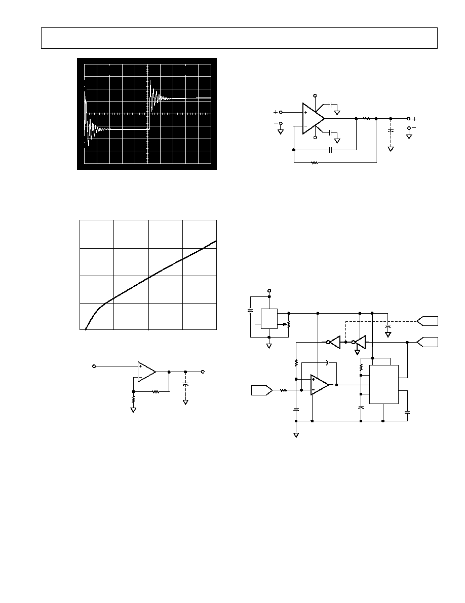
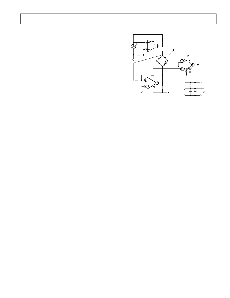
Low Dropout Bipolar Bridge Driver
The AD822 can be used for driving a 350
Wheatstone bridge.
Figure 10 shows one half of the AD822 being used to buffer
the AD589--a 1.235 V low power reference. The output of
4.5 V can be used to drive an A/D converter front end. The
other half of the AD822 is configured as a unity-gain inverter,
and generates the other bridge input of ≠4.5 V. Resistors R1
and R2 provide a constant current for bridge excitation. The
AD620 low power instrumentation amplifier is used to con-
dition the differential output voltage of the bridge. The gain
of the AD620 is programmed using an external resistor R
G
, and
determined by:
G
=
49.4 k
R
G
+ 1
+1.235V
49.9k
+Vs
1/2
AD822
AD620
1/2
AD822
TO A/D CONVERTER
REFERENCE INPUT
R1
20
25.4k 1%
10k
1%
350
350
350
350
R
G
AD589
10k
1%
10k
1%
R2
20
+Vs
≠4.5V
+Vs
≠Vs
GND
0.1 F
0.1 F
1 F
1 F
+5V
≠5V
V
REF
≠V
S
+
+
+
+
+V
S
Figure 10. Low Dropout Bipolar Bridge Driver
≠18≠
AD822
REV. B
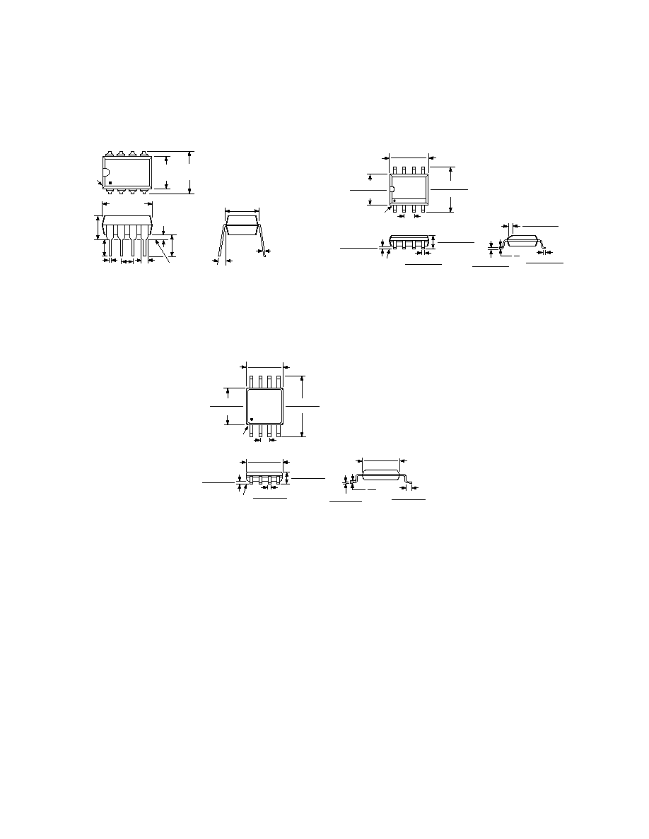
OUTLINE DIMENSIONS
Dimensions shown in inches and (mm).
PDIP Package
(N-8)
0.39 (9.91)
MAX
0.10
(2.54)
BSC
SEATING
PLANE
0.125 (3.18)
MIN
0.165 0.01
(4.19 0.25)
0.035 0.01
(0.89 0.25)
0.18 0.03
(4.57 0.76)
0.018 0.003
(0.46 0.08)
0.033
(0.84)
NOM
8
1
4
5
PIN 1
0.25
(6.35)
0.31
(7.87)
0.30 (7.62)
REF
0.011 0.003
(0.28 0.08)
0∞-15∞
SOIC Package
(SO-8)
0.0098 (0.25)
0.0075 (0.19)
0.0500 (1.27)
0.0160 (0.41)
8
0
0.0196 (0.50)
0.0099 (0.25)
45
8
5
4
1
0.1968 (5.00)
0.1890 (4.80)
0.2440 (6.20)
0.2284 (5.80)
PIN 1
0.1574 (4.00)
0.1497 (3.80)
0.0500 (1.27)
BSC
0.0688 (1.75)
0.0532 (1.35)
SEATING
PLANE
0.0098 (0.25)
0.0040 (0.10)
0.0192 (0.49)
0.0138 (0.35)
8-Lead Mini_SOIC
RM-8
0.011 (0.28)
0.003 (0.08)
0.028 (0.71)
0.016 (0.41)
33
27
0.120 (3.05)
0.112 (2.84)
8
5
4
1
0.122 (3.10)
0.114 (2.90)
0.199 (5.05)
0.187 (4.75)
PIN 1
0.0256 (0.65) BSC
0.122 (3.10)
0.114 (2.90)
SEATING
PLANE
0.006 (0.15)
0.002 (0.05)
0.018 (0.46)
0.008 (0.20)
0.043 (1.09)
0.037 (0.94)
0.120 (3.05)
0.112 (2.84)

≠19≠
Location
Page
Data sheet changed from REV. A to REV. B and all figures updated.
Cerdip References removed . . . . . . . . . . . . . . . . . . . . . . . . . . . . . . . . . . . . . . . . . . . . . . . . . . . . . . . . . . . . . . . . . . . . . . . . . . .1, 6, 18
Additions to Product Description . . . . . . . . . . . . . . . . . . . . . . . . . . . . . . . . . . . . . . . . . . . . . . . . . . . . . . . . . . . . . . . . . . . . . . . . . . .1
8-Lead SOIC and 8-Lead MSOP Diagrams added . . . . . . . . . . . . . . . . . . . . . . . . . . . . . . . . . . . . . . . . . . . . . . . . . . . . . . . . . . . . . 1
Deletion of AD822S column . . . . . . . . . . . . . . . . . . . . . . . . . . . . . . . . . . . . . . . . . . . . . . . . . . . . . . . . . . . . . . . . . . . . . . . . . . . . . 2≠5
Edits to Absolute Maximum Ratings and Ordering Guide . . . . . . . . . . . . . . . . . . . . . . . . . . . . . . . . . . . . . . . . . . . . . . . . . . . . . . . . 6
Removed Metalization Photograph . . . . . . . . . . . . . . . . . . . . . . . . . . . . . . . . . . . . . . . . . . . . . . . . . . . . . . . . . . . . . . . . . . . . . . . . . 6
RM-8 Package added to Outline Dimensions . . . . . . . . . . . . . . . . . . . . . . . . . . . . . . . . . . . . . . . . . . . . . . . . . . . . . . . . . . . . . . . . 18
Revision History≠AD822
REV. B

≠20≠
C00874≠0.2≠4/01(B)
PRINTED IN U.S.A.