 | –≠–ª–µ–∫—Ç—Ä–æ–Ω–Ω—ã–π –∫–æ–º–ø–æ–Ω–µ–Ω—Ç: AD8326 | –°–∫–∞—á–∞—Ç—å:  PDF PDF  ZIP ZIP |
Document Outline
- Specifications
- Pinout
- Package drawings
- Ordering Guide
- Features
- Applications
- Product Description
- Absolute Maximum Ratings
- Functional Block Diagram
- Pin Function Description
- Typical Characteristics
- CAUTION
- DIAGRAMS
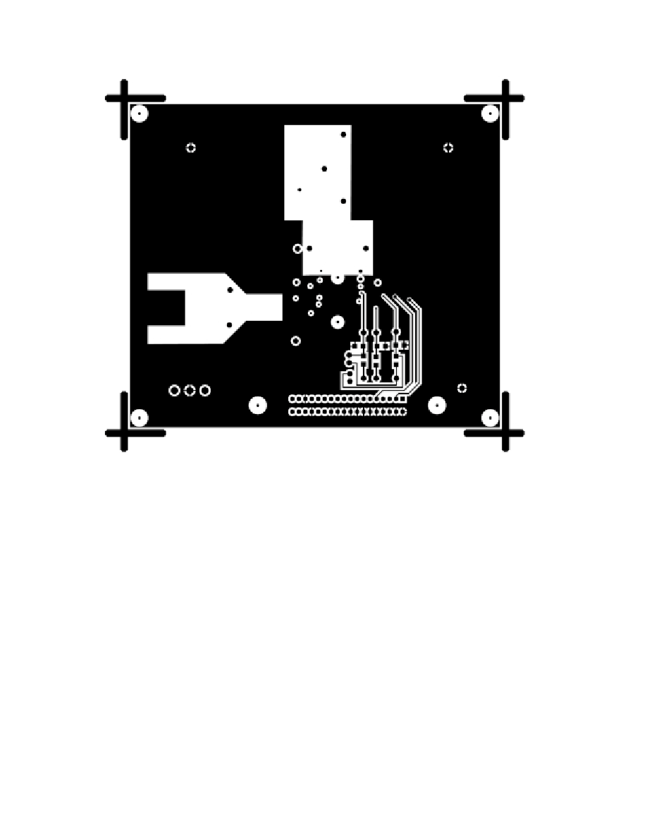
- Evaluation Board Layout (Component Side)
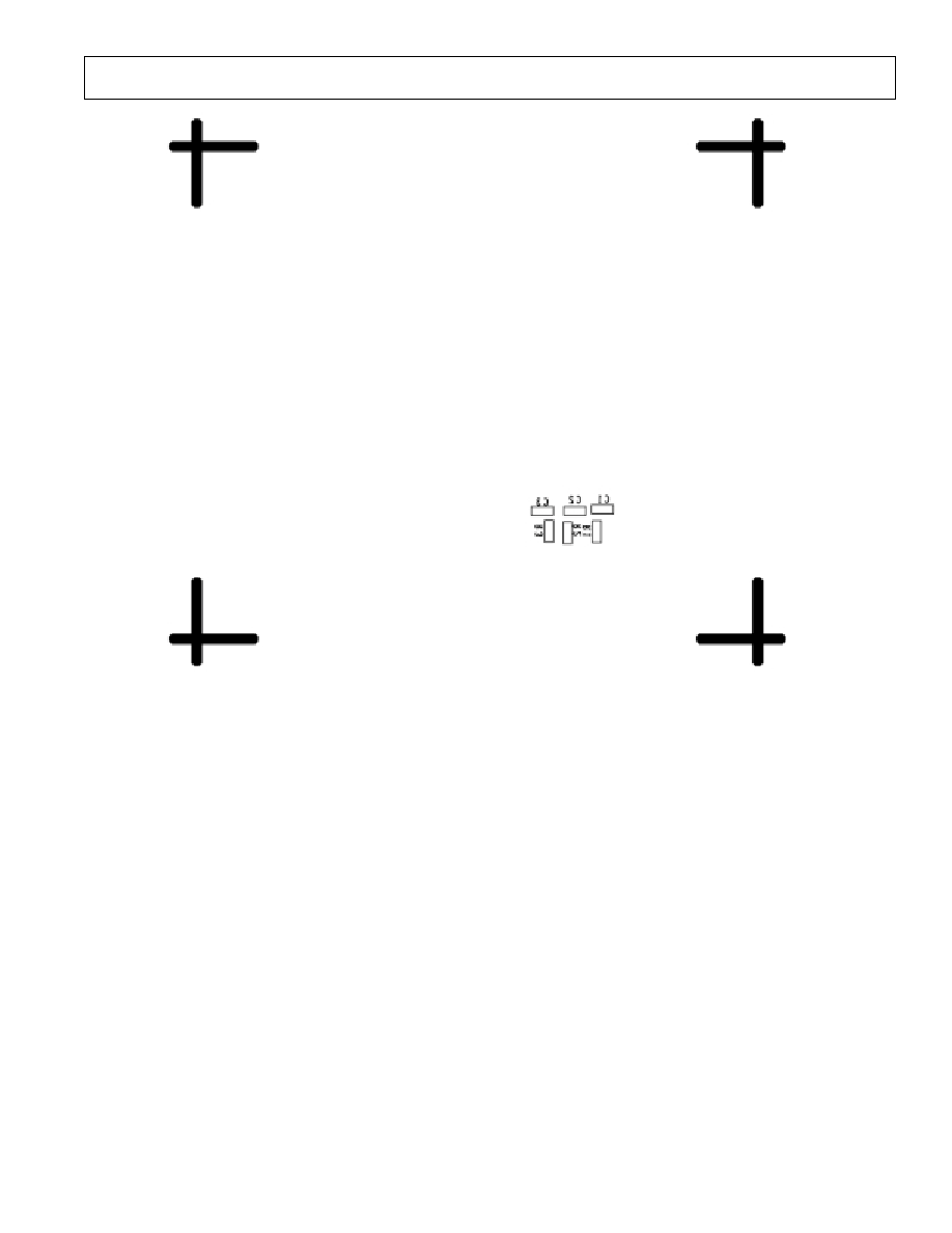
- Evaluation Board Layout (Silkscreen Top)
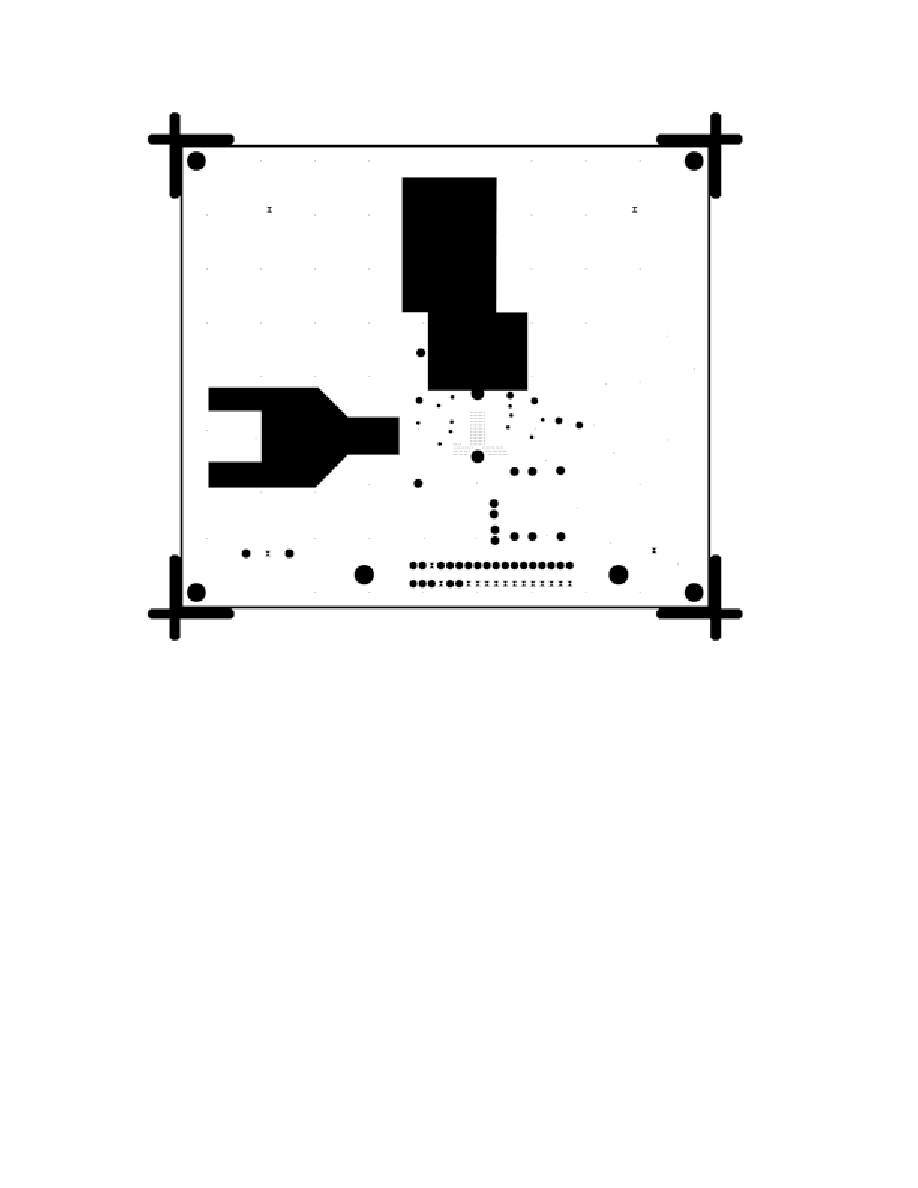
- Evaluation Board Layout (Circuit Side)
- Evaluation Board Layout (Silkscreen Bottom)
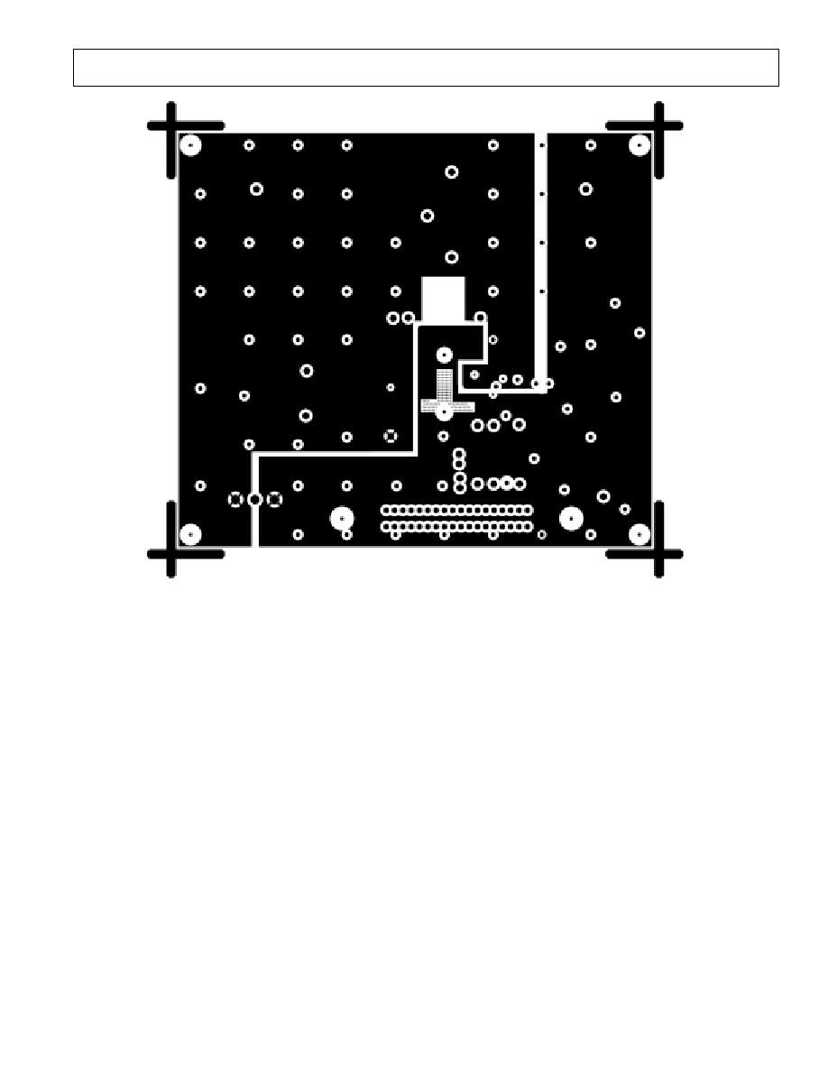
- Evaluation Board Layout (Internal Ground Plane)
- Evaluation Board Layout (Internal Power Planes)
- Evaluation Board Schematic
- Control Software Interface
- Parallel Port Selection
- Differential Input
- Single-Ended Input Impedance
- Typical Applications Circuit
- Differential Signal from Single-Ended Source
- Test Circuit
- SDATA Timing
- Serial Interface Timing
- Worst Harmonic Distortion vs. Frequency
REV. 0
Information furnished by Analog Devices is believed to be accurate and
reliable. However, no responsibility is assumed by Analog Devices for its
use, nor for any infringements of patents or other rights of third parties that
may result from its use. No license is granted by implication or otherwise
under any patent or patent rights of Analog Devices.
a
AD8326
One Technology Way, P.O. Box 9106, Norwood, MA 02062-9106, U.S.A.
Tel: 781/329-4700
www.analog.com
Fax: 781/326-8703
© Analog Devices, Inc., 2001
High Output Power
Programmable CATV Line Driver
FUNCTIONAL BLOCK DIAGRAM
DIFF OR
SINGLE
INPUT
AMP
ATTENUATION
CORE
Z
OUT
DIFF =
75
8
8
8
Z
IN
(SINGLE) = 800
Z
IN
(DIFF) = 1.6k
AD8326
DATEN
DATA
CLK
V
EE
(10 PINS)
TXEN
SLEEP
V
OUT+
V
OUT≠
V
CC
(7 PINS)
V
IN+
V
IN≠
VERNIER
DECODE
DATA LATCH
SHIFT
REGISTER
POWER-DOWN
LOGIC
POWER
AMP
BYP
GND
FEATURES
Supports DOCSIS Standard for Reverse Path
Transmission
Gain Programmable in 0.75 dB Steps over a 53.5 dB Range
Low Distortion at 65 dBmV Output
≠62 dBc SFDR at 21 MHz
≠58 dBc SFDR at 65 MHz
1 dB Compression of 25 dBm at 10 MHz
Output Noise Level
≠45 dBmV in 160 kHz
Maintains 75 Output Impedance
Power-Up and Power-Down Condition
Upper Bandwidth: 100 MHz (Full Gain Range)
Single or Dual Supply Operation
APPLICATIONS
Gain-Programmable Line Driver
CATV Telephony Modems
CATV Terminal Devices
General-Purpose Digitally Controlled Variable Gain Block
≠40
≠45
≠50
≠55
≠60
≠65
≠70
≠75
≠80
5 15 25 35 45 55 65
DISTORTION
≠
dBc
FREQUENCY ≠ MHz
ARP(V
S
= +12V)
ARE(V
S
= 5V)
ARP(V
O
= 69dBmV)
ARP(V
O
= 67dBmV)
ARE(V
O
= 65dBmV)
ARE(V
O
= 62dBmV)
Figure 1. Worst Harmonic Distortion vs. Frequency
GENERAL DESCRIPTION
The AD8326 is a high-output power, digitally controlled, vari-
able gain amplifier optimized for coaxial line driving applications
such as data and telephony cable modems that are designed to
the MCNS-DOCSIS upstream standard. An 8-bit serial word
determines the desired output gain over a 53.5 dB range result-
ing in gain changes of 0.75 dB/LSB. The AD8326 is offered in
two models, each optimized to support the desired output power
and resulting performance.
The AD8326 comprises a digitally controlled variable attenuator
of 0 dB to ≠54 dB, that is preceded by a low noise, fixed-gain
buffer and is followed by a low distortion high-power amplifier.
The AD8326 accepts a differential or single-ended input signal.
The output is designed to drive a 75
load, such as coaxial
cable, although the AD8326 is capable of driving other loads.
When driving 67 dBm into a 75
load, the AD8326ARP
provides a worst harmonic of only ≠59 dBc at 21 MHz and
≠57 dBc at 42 MHz. When driving 65 dBmV into a 75
load,
the AD8326ARE provides a worst harmonic of only ≠62 dBc at
21 MHz and ≠60 dBc at 42 MHz.
The differential output of the AD8326 is compliant with DOCSIS
paragraph 4.2.10.2 for "Spurious Emissions During Burst On/Off
Transients." In addition, this device has a sleep mode function
that reduces the quiescent current to 4 mA.
The AD8326 is packaged in a low-cost 28-lead TSSOP and a
28-lead P (power) SOIC. Both devices have an operational tem-
perature range of ≠40
∞
C to +85
∞
C.

REV. 0
≠2≠
AD8326≠SPECIFICATIONS
(T
A
= 25 C, V
S
= 12 V, R
L
= R
IN
= 75
, V
IN
= 259 mV p-p, V
OUT
measured through a 1:1
transformer
with an insertion loss of 0.5 dB @ 10 MHz, unless otherwise noted.)
AD8326ARP
Parameter
Conditions
Min
Typ
Max
Unit
INPUT CHARACTERISTICS
Specified AC Voltage
Output = 67 dBmV, Max Gain
259
mV p-p
Noise Figure
Max Gain, f = 10 MHz
16.6
dB
Input Resistance
Differential Input
1600
Single-Ended Input
800
Input Capacitance
2
pF
GAIN CONTROL INTERFACE
Gain Range
52.5
53.5
54.5
dB
Maximum Gain
Gain Code = 71 Dec
26.5
27.5
28.5
dB
Minimum Gain
Gain Code = 0 Dec
≠27
≠26
≠25
dB
Gain Scaling Factor
0.7526
dB/LSB
Gain Linearity Error
f = 10 MHz, Code-to-Code
±
0.2
dB
OUTPUT CHARACTERISTICS
Bandwidth (≠3 dB)
All Gain Codes
100
MHz
Bandwidth Roll-Off
f = 65 MHz
1.2
dB
Bandwidth Peaking
f = 65 MHz
0
dB
Output Noise Spectral Density
Max Gain, f = 10 MHz
≠28
dBmV in
160 kHz
Min Gain, f = 10 MHz
≠45.5
dBmV in
160 kHz
Transmit Disable Mode, f = 10 MHz
≠65
dBmV in
160 kHz
1 dB Compression Point
Max Gain, f = 10 MHz
26.5
dBm
Differential Output Impedance
Transmit Enable and Transmit Disable Mode
75
±
20%
OVERALL PERFORMANCE
Worst Harmonic Distortion
f = 14 MHz, V
OUT
= 67 dBmV @ Max Gain
≠59
dBc
f = 21 MHz, V
OUT
= 67 dBmV @ Max Gain
≠59
dBc
f = 42 MHz, V
OUT
= 67 dBmV @ Max Gain
≠57
dBc
f = 65 MHz, V
OUT
= 67 dBmV @ Max Gain
≠55
dBc
Adjacent Channel Power
16 QAM, V
OUT
= 67 dBmV
≠56
dBc
Adj Ch Wid = Tr Ch Wid = 160 KSYM/SEC
Output Settling
Due to Gain Change (T
GS
)
Min to Max Gain
60
ns
Due to Input Step Change
Max Gain, V
IN
= 0 V to 0.25 V p-p
30
ns
Signal Isolation
Min Gain, TXEN = 0, 65 MHz, V
IN
= 0.25 V p-p
≠85
dBc
Max Gain, TXEN = 0, 42 MHz, V
IN
= 0.25 V p-p
≠31
dBc
Max Gain, TXEN = 0, 65 MHz, V
IN
= 0.25 V p-p
≠28
dBc
All Gains, SLEEP, 65 MHz, V
IN
= 0.25 V p-p
≠85
dBc
POWER CONTROL
Transmit Enable Response Time (t
ON
)
Max Gain, V
IN
= 0
250
ns
Transmit Disable Response Time (t
OFF
) Max Gain, V
IN
= 0
40
ns
Between Burst Transients
1
Equivalent Output = 31 dBmV
5
mV p-p
Equivalent Output = 61 dBmV
60
mV p-p
POWER SUPPLY
Operating Range
11.4
12
12.6
V
Quiescent Current
Transmit Enable Mode (TXEN = 1)
147
157
167
mA
Transmit Disable Mode (TXEN = 0)
38
44
50
mA
Sleep Mode
1.5
4.5
7.5
mA
OPERATING TEMPERATURE
≠40
+85
∞
C
RANGE
NOTES
1
Between Burst Transients measured at the output of diplexer.
Specifications subject to change without notice.

REV. 0
AD8326
≠3≠
(T
A
= 25 C, V
S
= 5 V, R
L
= R
IN
= 75
, V
IN
= 206 V p-p, V
OUT
measured through a 1:1
transformer
with an insertion loss of 0.5 dB @ 10 MHz, unless otherwise noted.)
SPECIFICATIONS
AD8326ARE
Parameter
Conditions
Min
Typ
Max
Unit
INPUT CHARACTERISTICS
Specified AC Voltage
Output = 65 dBmV, Max Gain
206
mV p-p
Noise Figure
Max Gain, f = 10 MHz
16.6
dB
Input Resistance
Differential Input
1600
Single-Ended Input
800
Input Capacitance
2
pF
GAIN CONTROL INTERFACE
Gain Range
52.5
53.5
54.5
dB
Maximum Gain
Gain Code = 71 Dec
26.5
27.5
28.5
dB
Minimum Gain
Gain Code = 0 Dec
≠27
≠26
≠25
dB
Gain Scaling Factor
0.7526
dB/LSB
Gain Linearity Error
f = 10 MHz, Code-to-Code
±
0.2
dB
OUTPUT CHARACTERISTICS
Bandwidth (≠3 dB)
All Gain Codes
100
MHz
Bandwidth Roll-Off
f = 65 MHz
1.1
dB
Bandwidth Peaking
f = 65 MHz
0
dB
Output Noise Spectral Density
Max Gain, f = 10 MHz
≠28
dBmV in
160 kHz
Min Gain, f = 10 MHz
≠45.5
dBmV in
160 kHz
Transmit Disable Mode, f = 10 MHz
≠65
dBmV in
160 kHz
1 dB Compression Point
Max Gain, f = 10 MHz
25.0
dBm
Differential Output Impedance
Transmit Enable and Transmit Disable Mode
75
±
20%
OVERALL PERFORMANCE
Worst Harmonic Distortion
f = 14 MHz, V
OUT
= 65 dBmV @ Max Gain
≠62
dBc
f = 21 MHz, V
OUT
= 65 dBmV @ Max Gain
≠62
dBc
f = 42 MHz, V
OUT
= 65 dBmV @ Max Gain
≠60
dBc
f = 65 MHz, V
OUT
= 65 dBmV @ Max Gain
≠58
dBc
Adjacent Channel Power
16 QAM, V
OUT
= 65 dBmV
≠58
dBc
Adj Ch Wid = Tr Ch Wid = 160 KSYM/SEC
Output Settling
Due to Gain Change (T
GS
)
Min to Max Gain
60
ns
Due to Input Step Change
Max Gain, V
IN
= 0 V to 0.19 V p-p
30
ns
Signal Isolation
Min Gain, TXEN = 0, 65 MHz, V
IN
= 0.19 V p-p
≠85
dBc
Max Gain, TXEN = 0, 42 MHz, V
IN
= 0.19 V p-p
≠31
dBc
Max Gain, TXEN = 0, 65 MHz, V
IN
= 0.19 V p-p
≠28
dBc
All Gains, SLEEP, 65 MHz, V
IN
= 0.19 V p-p
≠85
dBc
POWER CONTROL
Transmit Enable Response Time (t
ON
)
Max Gain, V
IN
= 0
250
ns
Transmit Disable Response Time (t
OFF
) Max Gain, V
IN
= 0
40
ns
Between Burst Transients
1
Equivalent Output = 31 dBmV
5
mV p-p
Equivalent Output = 61 dBmV
60
mV p-p
POWER SUPPLY
Operating Range
±
4.75
±
5.0
±
5.25 V
Quiescent Current
Transmit Enable Mode (TXEN = 1)
140
150
160
mA
Transmit Disable Mode (TXEN = 0)
36
42
48
mA
Sleep Mode
1
4
7
mA
OPERATING TEMPERATURE
≠40
+85
∞
C
RANGE
NOTES
1
Between Burst Transients measured at the output of diplexer.
Specifications subject to change without notice.

REV. 0
AD8326
≠4≠
LOGIC INPUTS (TTL/CMOS Compatible Logic)
Parameter
Min
Typ
Max
Unit
Logic "1" Voltage
2.1
5.0
V
Logic "0" Voltage
0
0.8
V
Logic "1" Current (V
INH
= 5 V) CLK, SDATA,
DATEN
0
20
nA
Logic "0" Current (V
INL
= 0 V) CLK, SDATA,
DATEN
≠600
≠100
nA
Logic "1" Current (V
INH
= 5 V) TXEN
50
190
µ
A
Logic "0" Current (V
INL
= 0 V) TXEN
≠250
≠30
µ
A
Logic "1" Current (V
INH
= 5 V)
SLEEP
50
190
µ
A
Logic "0" Current (V
INL
= 0 V)
SLEEP
≠250
≠30
µ
A
Specifications subject to change without notice.
TIMING REQUIREMENTS
Parameter
Min
Typ
Max
Unit
Clock Pulsewidth (t
WH
)
16.0
ns
Clock Period (t
C
)
32.0
ns
Setup Time SDATA vs. Clock (t
DS
)
5.0
ns
Setup Time
DATEN vs. Clock (t
ES
)
15.0
ns
Hold Time SDATA vs. Clock (t
DH
)
5.0
ns
Hold Time
DATEN vs. Clock (t
EH
)
3.0
ns
Input Rise and Fall Times, SDATA,
DATEN, Clock (t
R
, t
F
)
10
ns
Specifications subject to change without notice.
t
ES
VALID DATA WORD G1
MSB. . . .LSB
GAIN TRANSFER (G1)
t
DS
t
EH
8 CLOCK CYCLES
GAIN TRANSFER (G2)
t
OFF
t
GS
ANALOG
OUTPUT
SIGNAL AMPLITUDE (p-p)
TXEN
CLK
SDATA
DATEN
t
ON
t
C
t
WH
VALID DATA WORD G2
Figure 2. Serial Interface Timing
VALID DATA BIT
MSB
MSB-1
MSB-2
t
DS
t
DH
SDATA
CLK
Figure 3. SDATA Timing
(Full Temperature Range, V
CC
= 12 V, t
R
= t
F
= 4 ns, f
CLK
= 8 MHz unless otherwise noted.)
(
DATEN, CLK, SDATA, TXEN, SLEEP, V
CC
= 12 V: Full Temperature Range)
REV. 0
AD8326
≠5≠
ORDERING GUIDE
Model
Temperature Range
Package Description
JA
Package Option
AD8326ARP
≠40
∞
C to +85
∞
C
28-Lead Power SOIC with Slug
23
∞
C/W
*
RP-28
AD8326ARP-REEL
AD8326ARP-EVAL
Evaluation Board
AD8326ARE
≠40
∞
C to +85
∞
C
28-Lead TSSOP with Exposed Pad
39
∞
C/W
*
RE-28
AD8326ARE-REEL
AD8326ARE-EVAL
Evaluation Board
*Thermal Resistance measured on SEMI standard 4-layer board.
ABSOLUTE MAXIMUM RATINGS
*
Supply Voltage V
CC
Pins 5, 9, 10, 19, 20, 23, 27 . For ARP, Max V
CC
= V
EE
+ 13 V;
. . . . . . . . . . . . . . . . . . . . . . . For ARE, Max V
CC
= V
EE
+ 11 V
Input Voltages
Pins 25, 26 . . . . . . . . . . . . . . . . . . . . . . . . . . . . . . . .
±
0.5 V
Pins 1, 2, 3, 6, 7 . . . . . . . . . . . . . . . . . . . . . ≠0.8 V to +5.5 V
Internal Power Dissipation
TSSOP EPAD . . . . . . . . . . . . . . . . . . . . . . . . . . . . . . 1.5 W
PSOP . . . . . . . . . . . . . . . . . . . . . . . . . . . . . . . . . . . . . . 2.0 W
Operating Temperature Range . . . . . . . . . . . ≠40
∞
C to +85
∞
C
Storage Temperature Range . . . . . . . . . . . . ≠65
∞
C to +150
∞
C
Lead Temperature, Soldering 60 seconds . . . . . . . . . . . 300
∞
C
*Stresses above those listed under Absolute Maximum Ratings may cause perma-
nent damage to the device. This is a stress rating only; functional operation of the
device at these or any other conditions above those indicated in the operational
section of this specification is not implied. Exposure to absolute maximum rating
conditions for extended periods may affect device reliability.
CAUTION
ESD (electrostatic discharge) sensitive device. Electrostatic charges as high as 4000 V readily
accumulate on the human body and test equipment and can discharge without detection. Although
the AD8326 features proprietary ESD protection circuitry, permanent damage may occur on
devices subjected to high-energy electrostatic discharges. Therefore, proper ESD precautions are
recommended to avoid performance degradation or loss of functionality.
WARNING!
ESD SENSITIVE DEVICE
REV. 0
AD8326
≠6≠
PIN FUNCTION DESCRIPTIONS
Pin No.
Mnemonic
Description
1
DATEN
Data Enable Low Input. This port controls the 8-bit parallel data latch and shift register. A Logic
0-to-1 transition transfers the latched data to the attenuator core (updates the gain) and simulta-
neously inhibits serial data transfer into the register. A 1-to-0 transition inhibits the data latch
(holds the previous gain state) and simultaneously enables the register for serial data load.
2
SDATA
Serial Data Input. This digital input allows for an 8-bit serial (gain) word to be loaded into the
internal register with the MSB (Most Significant Bit) first and ignored.
3
CLK
Clock Input. The clock port controls the serial attenuator data transfer rate to the 8-bit master-
slave register. A Logic 0-to-1 transition latches the data bit and a 1-to-0 transfers the data bit to
the slave. This requires the input serial data word to be valid at or before this clock transition.
4, 28
GND
Common External Ground Reference
5, 9, 10, 19,
V
CC
Common Positive External Supply Voltage. A 0.1
µ
F capacitor must decouple each pin.
20, 23, 27
6
TXEN
Transmit Enable pin. Logic 1 powers up the part.
7
SLEEP
Low Power Sleep Mode. In the Sleep mode, the AD8326's supply current is reduced to 4 mA. A
Logic 0 powers down the part (High Z
OUT
State) and a Logic 1 powers up the part.
8, 12, 17
NC
No Connection to these pins.
11, 13, 16, 18,
V
EE
Common Negative External Supply Voltage. A 0.1
µ
F capacitor must decouple each pin.
22, 24
14
OUT≠
Negative Output Signal
15
OUT+
Positive Output Signal
21
BYP
Internal Bypass. This pin must be externally ac-coupled (0.1
µ
F capacitor).
25
V
IN+
Noninverting Input. DC-biased to approximately V
CC
/2. Should be ac-coupled with a
0.1
µ
F capacitor.
26
V
IN≠
Inverting Input. DC-biased to approximately V
CC
/2. Should be ac-coupled with a 0.1
µ
F capacitor.
PIN CONFIGURATION
TOP VIEW
(Not to Scale)
28
27
26
25
24
23
22
21
20
19
18
17
16
15
1
2
3
4
5
6
7
8
9
10
11
12
13
14
AD8326
DATEN
GND
SDATA
V
CC
CLK
V
IN≠
GND
V
IN+
V
CC
V
EE
TXEN
V
CC
SLEEP
V
EE
NC
BYP
V
CC
V
CC
V
CC
V
CC
V
EE
V
EE
NC
NC
V
EE
V
EE
OUT≠
OUT+
NC = NO CONNECT
REV. 0
AD8326
≠7≠
1.0
0.5
0
≠0.5
≠1.0
≠1.5
0 9 18 27 36 45 54 63 72
GAIN CONTROL ≠ Decimal
GAIN ERROR
≠
dB
V
S
= 12V
P
O
= 67dBmV@ MAX GAIN
65MHz
42MHz
5MHz
10MHz
TPC 2. Gain Error vs. Gain Control
40
30
20
10
0
≠10
≠20
≠30
≠40
0.1 1 10 100 1000
GAIN
≠
dB
FREQUENCY ≠ MHz
71D
00D
46D
V
S
= 12V
V
O
= 67dBmV @ MAX GAIN
23D
TPC 3. AC Response
Typical Performance Characteristics≠
V
IN+
V
IN≠
V
CC
V
EE
OUT≠
AD8326
BYP
OUT+
0.1 F
0.1 F
1:1
TOKO
617DB-A0070
C
L
0.1 F
0.1 F
165
75
75
75
+
≠
V
O
V
CC
10 F
0.1 F
+1/2 V
IN
≠1/2 V
IN
0.1 F
0.1 F
10 F
V
EE
TPC 1. Test Circuit
1
10
100
32.0
30.5
29.0
27.5
26.0
24.5
23.0
21.5
GAIN
≠
dB
FREQUENCY ≠ MHz
C
L
= 0pF
C
L
= 10pF
C
L
= 20pF
C
L
= 50pF
V
S
= 12V
P
OUT
= 67dBmV @ MAX GAIN
TPC 4. AC Response for Various Capacitor Loads
≠26
≠30
≠34
≠38
≠42
≠46
≠50
GAIN CONTROL ≠ Decimal
OUTPUT NOISE
≠
dBmV in 160 kHz
0 8 16 24 32 40 48 56 64 72
f = 10MHz
TXEN = 1
V
S
= 12V
TPC 5. Output Referred Noise vs. Gain Control
REV. 0
AD8326
≠8≠
≠50
≠55
≠60
≠65
≠70
≠75
≠80
≠85
≠90
0 9 18 27 36 45 54 63 72
DISTORTION
≠
dBc
GAIN CODE ≠ Decimal
V
S
= 12V
f
= 42MHz
P
O
= 67dBmV @ MAX GAIN
HD3
HD2
TPC 6. Harmonic Distortion vs. Gain Code for
AD8326-ARP
≠50
≠55
≠60
≠65
≠70
≠75
≠80
≠85
≠90
5 15 25 35 45 55 65
DISTORTION
≠
dBc
FREQUENCY ≠ MHz
V
O
= 68dBmV @ MAX GAIN
V
O
= 69dBmV @ MAX GAIN
V
O
= 67dBmV @ MAX GAIN
V
O
= 65dBmV @ MAX GAIN
V
S
= 12V(ARP)
TPC 7. Second Order Harmonic Distortion vs. Frequency
for Various Output Powers
≠35
≠40
≠45
≠50
≠55
≠60
≠65
≠70
≠75
5 15 25 35 45 55 65
V
S
= +12V(ARP)
V
O
= 69dBmV @ MAX GAIN
V
O
= 67dBmV @ MAX GAIN
V
O
= 65dBmV @ MAX GAIN
V
O
= 68dBmV @ MAX GAIN
DISTORTION
≠
dBc
FREQUENCY ≠ MHz
TPC 8. Third Order Harmonic Distortion vs. Frequency
for Various Output Powers
0
≠10
≠20
≠30
≠40
≠50
≠60
≠70
≠80
≠90
≠100
CENTER 21MHz
100kHz/
SPAN 1MHz
RBW 500Hz RF ATT 30dB
VBW 5kHz
SWT 20s UNIT dBm
CH PWR +12.27dBm
ACP UP ≠56.72dB
ACP LOW ≠56.71dB
TPC 9. Adjacent Channel Power for AD8326-ARP
190
180
170
160
150
140
130
120
110
1 10 100 1000
IMPEDANCE
≠
FREQUENCY ≠ MHz
POWER-DOWN
POWER-UP
SLEEP
TPC 10. Input Impedance vs. Frequency (Inputs
Shunted with 165
)
1000
100
10
1
0.1 1 10 100 1000
IMPEDANCE
≠
FREQUENCY ≠ MHz
SLEEP
POWER-DOWN
POWER-UP
TPC 11. Output Impedance vs. Frequency
REV. 0
AD8326
≠9≠
DISTORTION
≠
dBc
≠50
≠55
≠60
≠65
≠70
≠75
≠80
≠85
≠90
0 9 18 27 36 45 54 63 72
DEC CODE
V
S
= 5V
f
= 42MHz
P
O
= 65dBmV @ MAX GAIN
HD3
HD2
TPC 12. Harmonic Distortion vs. Gain Control for
AD8326-ARE
≠50
≠55
≠60
≠65
≠70
≠75
≠80
≠85
≠90
5 15 25 35 45 55 65
V
S
= 5V(ARE)
V
O
= 65dBmV @ MAX GAIN
V
O
= 66dBmV @ MAX GAIN
V
O
= 64dBmV @ MAX GAIN
V
O
= 62dBmV @ MAX GAIN
DISTORTION
≠
dBc
FREQUENCY ≠ MHz
TPC 13. Second Order Harmonic Distortion vs. Frequency
for Various Output Powers
≠40
≠45
≠50
≠55
≠60
≠65
≠70
≠75
≠80
5 15 25 35 45 55 65
DISTORTION
≠
dBc
FREQUENCY ≠ MHz
V
O
= 66dBmV @ MAX GAIN
V
O
= 65dBmV @ MAX GAIN
V
O
= 64dBmV @ MAX GAIN
V
O
= 62dBmV @ MAX GAIN
V
S
= 5V(ARE)
TPC 14. Third Order Harmonic Distortion vs. Frequency
for Various Output Powers
0
≠10
≠20
≠30
≠40
≠50
≠60
≠70
≠80
≠90
≠100
CENTER 21MHz
100kHz/
SPAN 1MHz
RBW 500Hz RF ATT 30dB
VBW 5kHz
SWT 20s UNIT dBm
CH PWR +10.41dBm
ACP UP ≠58.83dB
ACP LOW ≠59.06dB
TPC 15. Adjacent Channel Power for AD8326-ARE
0
≠20
≠40
≠60
≠80
≠100
≠120
0 10 100 1000
ISOLATION
≠
dBc
FREQUENCY ≠ MHz
V
S
= 12V
TXEN = 1
TXEN = 0
SLEEP
TPC 16. Signal Isolation vs. Frequency
200
180
160
140
120
100
80
60
40
20
≠40 ≠30 ≠20 ≠10 0 10 20 30 40 50 60 70 80 90
TEMPERATURE ≠ C
SUPPLY CURRENT
≠
mA
V
S
= 12V(ARP)
TRANSMIT ENABLE
TRANSMIT DISABLE
TPC 17. Quiescent Current vs. Temperature
REV. 0
AD8326
≠10≠
APPLICATIONS
General Applications
The AD8326 is primarily intended for use as the upstream
power amplifier (PA), also known as a line driver, in DOCSIS
(Data Over Cable Service Interface Specification) certified
cable modems, cable telephony systems, and CATV set-top
boxes. The upstream signal is either a QPSK or QAM signal
generated by a DSP, a dedicated QPSK/QAM modulator, or a
DAC. In all cases the signal must be low-pass filtered before
being applied to the PA in order to filter out-of-band noise and
higher order harmonics from the amplified signal. Due to the
varying distances between the cable modem and the headend,
the upstream PA must be capable of varying the output power
by applying gain or attenuation. The varying output power of
the AD8326 ensures that the signal from the cable modem will
have the proper level once it arrives at the headend. The upstream
signal path also contains a transformer, a diplexer, and cable split-
ters. The AD8326 has been designed to overcome losses associated
with these passive components in the upstream cable path, particu-
larly in modems that support cable telephony.
AD8326ARP Applications
The AD8326ARP is in a thermally enhanced PSOP2 package,
and designed for single 12 V supply and output power applica-
tions up to +69 dBmV. The AD8326ARP will provide maximum
performance in 12 V systems.
AD8326ARE Applications
The AD8326ARE is in a TSSOP package with an exposed ther-
mal pad. It is designed for dual
±
5 V or single 10 V supplies. For
applications requiring up to 65 dBmV of output power, lower
cost, smaller package, and lower power dissipation, the TSSOP
package is most appropriate.
Operational Description
The AD8326 consists of four analog functions in the transmit
enable or forward mode. The input amplifier (preamp) can be
used single-ended or differentially. If the input is used in the
differential configuration, it is imperative that the input signals be
180 degrees out of phase and of equal amplitudes. This will
ensure proper gain accuracy and harmonic performance. The
preamp stage drives a vernier stage that provides the fine tune
gain adjustment. The approximate step resolution of 0.75 dB is
implemented in this stage and provides a total of approximately
5.25 dB of accumulated attenuation. After the vernier stage, a
DAC provides the bulk of the AD8326's attenuation (8 bits or
48 dB). The signals in the preamp and vernier gain blocks are
differential to improve the PSRR and linearity. A differential
current is fed from the DAC into the output stage, which
amplifies these currents to the appropriate levels necessary to
drive a 75
load.
The output stage utilizes negative feedback to implement a
differential 75
output impedance, which eliminates the need
for external matching resistors needed in typical video (or
video filter) termination requirements.
SPI Programming
The AD8326 is controlled through a serial peripheral interface
(SPI) of three digital data lines, CLK,
DATEN, and SDATA.
Changing the gain requires 8 bits of data to be streamed into the
SDATA port. The sequence of loading the SDATA register
begins on the falling edge of the
DATEN pin, which activates
the CLK line. With the CLK line activated, data on the SDATA
line is clocked into the serial shift register, Most Significant Bit
(MSB) first, on the rising edge of the CLK pulses. Since a 7-bit
shift register is used in the AD8326, the MSB of the 8-bit word
is a "don't care" bit and is shifted out of the register on the eighth
clock pulse. The data is latched into the attenuator core on the
rising edge of the
DATEN line. This provides control over the
changes in the output signal level. The serial interface timing for
the AD8326 is shown in Figures 2 and 3. The programmable
gain range of the AD8326 is ≠25.75 dB to +27.5 dB with steps
of 0.75 dB. This provides a total gain range of 53.25 dB. The
AD8326 was characterized with a TOKO transformer (TOKO
#617DB-A0070), and the stated gain values include the losses
due to the transformer.
For gain codes from 0 through 71 the gain transfer function is:
A
dB
dB
CODE
V
=
◊
[
]
27 5
0 75
71
.
≠ ( .
(
≠
)
where A
V
is the gain in dB and CODE is the decimal equivalent
of the 8-bit word. Gain codes 0 to 71 provide linear changes in
gain. Figure 4 shows the gain characteristics of the AD8326 for
all possible values in an 8-bit word. Note that maximum gain is
achieved at Code 71. From Code 72 through 127 the 5.25 dB
of attenuation from the vernier stage is being applied over every
eight codes, resulting in the saw tooth characteristic at the top
of the gain range. Because the eighth bit is shifted out of the
register, the gain characteristics for Codes 128 through 255 are
identical to Codes 0 through 127, as depicted in Figure 4.
28
21
14
7
0
≠7
≠14
≠21
≠28
0 32 64 96 128 160 192 224 256
GAIN
≠
dB
GAIN CODE ≠ Decimal
Figure 4. Gain Code vs. Gain
REV. 0
AD8326
≠11≠
Input Bias, Impedance, and Termination
The V
IN
+ and V
IN
≠ inputs have a dc bias level of approxi-
mately 1.47 V below V
CC
/2, therefore the input signal should
be ac-coupled using 0.1
µ
F capacitors as seen in the typical
application circuit (see Figure 5).
The differential input impedance of the AD8326 is approxi-
mately 1600
, while the single-ended input is 800
.
Single-Ended Inverting Input
When operating the AD8326 in a single-ended input mode V
IN
+
and V
IN
≠ should be terminated as illustrated in Figure 6. On the
AD8326 evaluation boards, this termination method requires the
removal of R12, R13, R14, R16, R17, and R18. Install a 0
jumper at R15, an 82.5
resistor at R10 for a 75
system, and a
39.2
resistor at R11 to balance the inputs of the AD8326
evaluation board (Figure 11). Other input impedance configura-
tions may be calculated using the equations in Figure 6.
AD8326
R10
R11
+
≠
Z
IN
= R10||800
R11 = Z
IN
||R10
V
IN
≠
Figure 6. Single-Ended Input Impedance
The inverting and noninverting inputs of the AD8326 must be
balanced for all input configurations.
Differential Input from Single-Ended Source
The default configuration of the evaluation board implements a
differential signal drive from a single-ended signal source. A
Toko 1:1 transformer is included on the board for this purpose
(T3). Enabling the evaluation board for single to differential
input conversion requires R15≠R17 to be removed, and 0
jumpers must be installed on the placeholders for R13, R14, and
R18. For a 75
input impedance, R12 should be 78.7
. Refer
to Figure 11 for evaluation board schematic. In this configuration,
the input signal must be applied to V
IN
≠. Other input imped-
ances may be calculated using the equation in Figure 7.
V
IN
≠
AD8326
DESIRED IMPEDANCE = R12||1600
R12
Figure 7. Differential Signal from Single-Ended Source
Differential Signal Source
The AD8326 evaluation board is also capable of accepting a
differential input signal. This requires the installation of a 165
resistor in R12, the removal of R13≠R14, R17≠R18, and the
installation of 0
jumpers for R15≠R16. This configuration
results in a differential input impedance of 150
. Other differ-
ential input impedance configurations may be calculated with
the equation in Figure 8.
V
IN
+
AD8326
V
IN
≠
R12
DESIRED IMPEDANCE = R12||1600
Figure 8. Differential Input
DATEN
SDATA
CLK
GND1
V
CC
TXEN
SLEEP
GND
V
CC
V
CC
V
EE
GND
V
EE
V
OUT≠
GND
V
CC
V
IN≠
V
IN+
V
EE
V
CC
V
EE
BYP
V
CC
V
CC
V
EE
GND
V
EE
V
OUT+
AD8326
V
EE
TXEN
DATEN
SDATA
CLK
10 F
0.1 F
0.1 F
0.1 F
TOKO 617DB-A0070
TO DIPLEXER
Z
IN
= 75
0.1 F
0.1 F
0.1 F
0.1 F
0.1 F
165
V
IN≠
V
IN+
Z
IN
= 150
10 F
V
CC
1
2
3
4
5
6
7
8
9
10
11
12
13
14
28
27
26
25
24
23
22
21
20
19
18
17
16
15
SLEEP
0.1 F
0.1 F
0.1 F
0.1 F
0.1 F
0.1 F
0.1 F
0.1 F
Figure 5. Typical Applications Circuit

REV. 0
AD8326
≠12≠
Output Bias, Impedance, and Termination
The outputs have a dc bias level of approximately V
CC
/2, there-
fore they should be ac-coupled before being applied to the load.
The differential output impedance of the AD8326 is internally
maintained at 75
, regardless of whether the amplifier is in
transmit enable mode or transmit disable mode, eliminating the
need for external back termination resistors. A 1:1 transformer
is used to couple the amplifier's differential output to the coaxial
cable while maintaining a proper impedance match. If the out-
put signal is being evaluated on standard 50
test equipment, a
minimum loss 75
≠50
pad must be used to provide the test
circuit with proper impedance match.
Single Supply Operation
The 12 V supply should be delivered to each of the V
CC
pins via
a low impedance power bus to ensure that each pin is at the
same potential. The power bus should be decoupled to ground using
a 10
µ
F tantalum capacitor located close to the AD8326ARP.
In addition to the 10
µ
F capacitor, each V
CC
pin should be
individually decoupled to ground with 0.1
µ
F ceramic chip
capacitors located close to the pins. The pin labeled BYP (Pin
21) should also be decoupled with a 0.1
µ
F capacitor. The PCB
should have a low-impedance ground plane covering all unused
portions of the board, except in the area of the input and output
traces in close proximity to the AD8326 and output transformer. All
ground and V
EE
pins of the AD8326ARP must be connected to
the ground plane to ensure proper grounding of all internal nodes.
Pin 28 and the exposed pad should be connected to ground.
Dual Supply Operation
The +5 V supply power should be delivered to each of the V
CC
pins via a low impedance power bus to ensure that each pin is at
the same potential. The ≠5 V supply should also be delivered to
each of the V
EE
pins with a low impedance bus. The power buses
should be decoupled to ground with a 10
µ
F tantalum capacitor
located close to the AD8326ARE. In addition to the 10
µ
F capaci-
tor, all V
CC
, V
EE
and BYP pins should be individually decoupled to
ground with 0.1
µ
F ceramic chip capacitors located close to the
pins. The PCB should have a low-impedance ground plane
covering all unused portions of the board, except in the area of
the input and output traces in close proximity to the AD8326
and output transformer. All ground pins of the AD8326ARE must
be connected to the ground plane to ensure proper grounding of
all internal nodes. Pin 28 and the exposed thermal pad should
both be tied to ground.
Signal Integrity Layout Considerations
Careful attention to printed circuit board layout details will
prevent problems due to board parasitics. Proper RF design
technique is mandatory. The differential input and output traces
should be kept as short as possible. It is also critical to make
sure that all differential signal paths are symmetrical in length
and width. In addition, the input and output traces should be
kept far apart in order to minimize coupling (crosstalk) through
the board. Following these guidelines will improve the overall
performance of the AD8326 in all applications.
Thermal Layout Considerations
As integrated circuits become denser, smaller, and more power-
ful, they often produce more heat. Therefore when designing PC
boards, the layout must be able to draw heat away from the higher
power devices. The AD8326ARE draws up to 1.5 W when running
at +65 dBmV with
±
5 V supplies. The AD8326ARP draws a
maximum of 2 W at +67 dBmV with a +12 V supply.
The following guidelines should be used for both the AD8326ARE
and AD8326ARP.
First and foremost, the exposed thermal pad should be soldered
directly to a substantial ground plane that adequately absorbs
heat away from the AD8326 package. This is the simplest, and
most important step in thermally managing the power dissipated in
the AD8326. Increasing the area of copper beneath the AD8326
will lower the thermal resistance in the PCB and more effectively
allow air to remove the heat from the PCB, and consequently,
from the AD8326.
Secondly, thermal stitching is a method for increasing thermal
capacity of the PCB. Additionally, thermal stitching can be used
to provide a thermally efficient area onto which the AD8326
may be soldered. Thermal stitching is accomplished by using a
number of plated through holes (or vias) densely populated in
the solder pad area (but not confined to the size of the TSSOP
or PSOP2 exposed thermal pad). This technique maximizes the
copper area where the package is attached to the PCB increas-
ing the thermal mass or capacity by utilizing more than one
copper plane. This method of thermal management should be
applied in close proximity to the exposed thermal pad.
Another important guideline is to utilize a multilayer PCB with
the AD8326. Lowering the PCB thermal resistance using several
layers will generally increase thermal mass resulting in cooler
junction temperatures.
Using the techniques described above and dedicating 2.9 square
inches of thermally enhanced PCB area, the AD8326 in either
package can operate at safe junction temperatures. Figures 12-17
show the above practices in use on the AD8326ARE-EVAL board.
Initial Power-Up
When the supply is first applied to the AD8326, the gain setting
of the amplifier is indeterminate. Therefore, as power is first
applied to the amplifier, the TXEN pin should be held low
(Logic 0), preventing forward signal transmission. After power
has been applied to the amplifier, the gain can be set to the desired
level by following the procedure in the SPI Programming and
Gain Adjustment section. The TXEN pin can then be brought
from Logic 0 to Logic 1, enabling forward signal transmission at
the desired gain level.
Asynchronous Power-Down
The asynchronous TXEN pin is used to place the AD8326 into
"Between Burst" mode while maintaining a differential output
impedance of 75
. Applying Logic 0 to the TXEN pin acti-
vates the on-chip reverse amplifier, providing a 72% reduction
in consumed power. For 12 V operation, the supply current is
typically reduced from 159 mA to 44 mA. In this mode of
operation, between burst noise is minimized and the amplifier
can no longer transmit in the upstream direction. In addition
to the TXEN pin, the AD8326 also incorporates an asynchro-
nous
SLEEP pin, which may be used to further reduce the supply current
to approximately 4 mA. Applying Logic 0 to the
SLEEP pin
places the amplifier into
SLEEP mode. Transitioning into or
out of
SLEEP mode will result in a transient voltage at the
output of the amplifier.

REV. 0
AD8326
≠13≠
Distortion, Adjacent Channel Power, and DOCSIS
In order to deliver +58 dBmV of high fidelity output power
required by DOCSIS, the PA is required to deliver up to
+67 dBmV. This added power is required to compensate for
losses associated with the transformer, diplexer, directional
coupler, and splitters that may be included in the upstream
path of the cable telephony. It should be noted that the AD8326
was characterized with the TOKO 617DB-A0070 transformer.
TPC 7, TPC 8, TPC 13, and TPC 14 show the AD8326 second
and third harmonic distortion performance versus fundamental
frequency for various output power levels. These figures are
useful for determining the in band harmonic levels from 5 MHz
to 65 MHz. Harmonics higher in frequency will be sharply
attenuated by the low-pass filter function of the diplexer.
Another measure of signal integrity is adjacent channel power,
commonly referred to as ACP. DOCSIS section 4.2.10.1.1
states, "Spurious emissions from a transmitted carrier may
occur in an adjacent channel that could be occupied by a carrier
of the same or different symbol rates." TPC 9 shows the mea-
sured ACP for a +67 dBmV 16 QAM signal taken at the output
of the AD8326 evaluation board, through a 75
to 50
matching pad (5.7 dB of loss). The transmit channel width
and adjacent channel width in TPC 9 correspond to symbol
rates of 160 KSYM/SEC. Table I shows the ACP results for
the AD8326 for all conditions in DOCSIS Table 4-7 "Adjacent
Channel Spurious Emissions."
Table I. Adjacent Channel Power
Adjacent Channel Symbol Rate
Transmit
160K/s
320K/s
640K/s
1280K/s 2560K/s
Symbol
ACP
ACP
ACP
ACP
ACP
Rate
(dBc)
(dBc)
(dBc)
(dBc)
(dBc)
160K/s
≠57
≠59
≠62
≠63
≠64
320K/s
≠57
≠58
≠60
≠62
≠64
640K/s
≠55
≠58
≠58
≠60
≠62
1280K/s
≠55
≠57
≠58
≠58
≠60
2560K/s
≠53
≠56
≠57
≠57
≠57
Noise and DOCSIS
At minimum gain, the AD8326 output noise spectral density is
13.3 nV/
Hz measured at 10 MHz. DOCSIS Table 4-8, "Spuri-
ous Emissions in 5 MHz to 42 MHz," specifies the output noise
for various symbol rates. The calculated noise power in dBmV
for 160 KSYM/SECOND is:
Comparing the computed noise power of ≠45.5 dBmV to the
+8 dBmV signal yields ≠53.5 dBc, which meets the required level
set forth in DOCSIS Table 4-8. As the AD8326 gain is increased
from this minimum value, the output signal increases at a faster
rate than the noise, resulting in a signal to noise ratio that improves
with gain. In transmit disable mode, the output noise spectral
density is 1.4 nV/
Hz, which results in ≠65 dBmV when computed
over 160
KSYM/SECOND
.
The noise power was measured directly at the output of the
transformer. In a typical cable telephony application there will
be a 6 dB pad, or splitter, which will further attenuate the noise
by 6 dB.
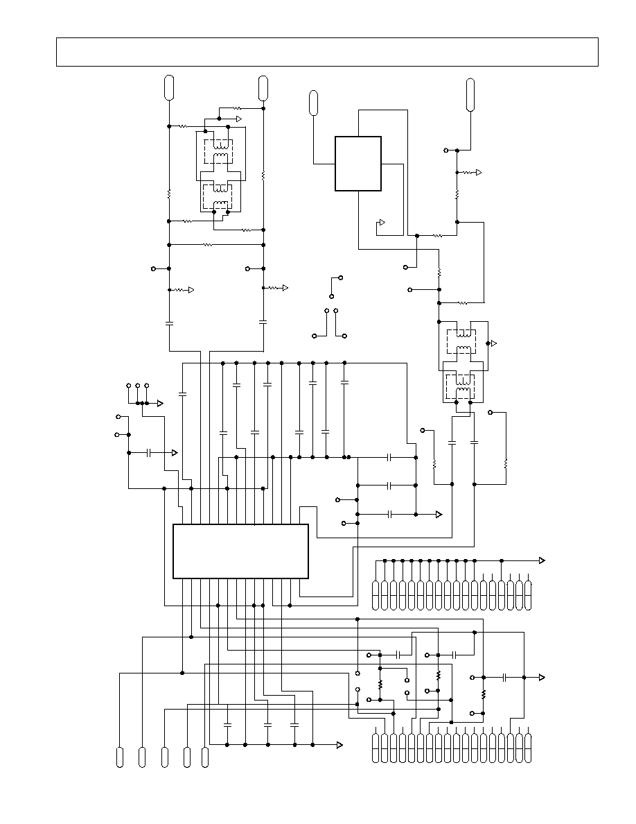
Evaluation Board Features and Operation
The AD8326 evaluation boards (Part # AD8326ARE-EVAL
and AD8326ARP-EVAL) and control software can be used to
control the AD8326 upstream cable driver via the parallel port
of a PC. A standard printer cable connected between the paral-
lel port and the evaluation board is used to feed all the necessary
data to the AD8326 by means of the Windows 9X-based control
software. This package provides a means of evaluating the amplifier
by providing a convenient way to program the gain/attenuation
as well as offering easy control of the asynchronous TXEN and
SLEEP pins. With this evaluation kit, the AD8326 can be evalu-
ated in either a single-ended or differential input configuration.
The amplifier can also be evaluated with or without the PULSE
diplexer in the output signal path. A schematic of the evaluation
board is provided in Figure 11.
Output Transformer and Diplexer
A 1:1 transformer is needed to couple the differential outputs of
the AD8326 to the cable while maintaining a proper impedance
match. The specified transformer is available from TOKO (Part
# 617DB-A0070); however, M/A-COM part # ETC-1-1T may
also be used. The evaluation board is equipped with the TOKO
transformer, but is also designed to accept the M/A-COM trans-
former. The PULSE diplexer included on the evaluation board
provides a high-order low-pass filter function, typically used in the
upstream path. To remove the diplexer from the signal path,
remove the 0
chip resistors at R7 and R19, and install a 0
chip resistor at R6 so the output signal is directed away from
the diplexer and toward the CABLE port of the evaluation
board (Figure 11). The ability of the PULSE diplexer to achieve
DOCSIS compliance is neither expressed nor implied by Analog
Devices Inc. Data on the diplexer should be obtained from
PULSE. When using the diplexer, be sure to properly terminate
the cable port (75
) so that the AD8326 draws minimal current.
Overshoot on PC Printer Ports
The data lines on some PC parallel printer ports have excessive
overshoot that may cause communications problems when pre-
sented to the CLK pin of the AD8326. The evaluation board
was designed to accommodate a series resistor and shunt capaci-
tor (R2 and C2 in Figure 11) to filter the CLK signal if required.
Installing Visual Basic Control Software
Install the "CabDrive_26" software by running "setup.exe" on
disk one of the AD8326 Evaluation Software. Follow on-screen
directions and insert disk two when prompted. Choose instal-
lation directory, and then select the icon in the upper left to
complete installation.
20
13 3
160
60
45 5
2
◊
◊
+
=
log
.
≠
.
nV
Hz
kHz
dBmV
REV. 0
AD8326
≠14≠
Running AD8326 Software
To load the control software, go to START, PROGRAMS,
CABDRIVE_26, or select the AD8326.exe from the installed
directory. Once loaded, select the proper parallel port to com-
municate with the AD8326 (Figure 9).
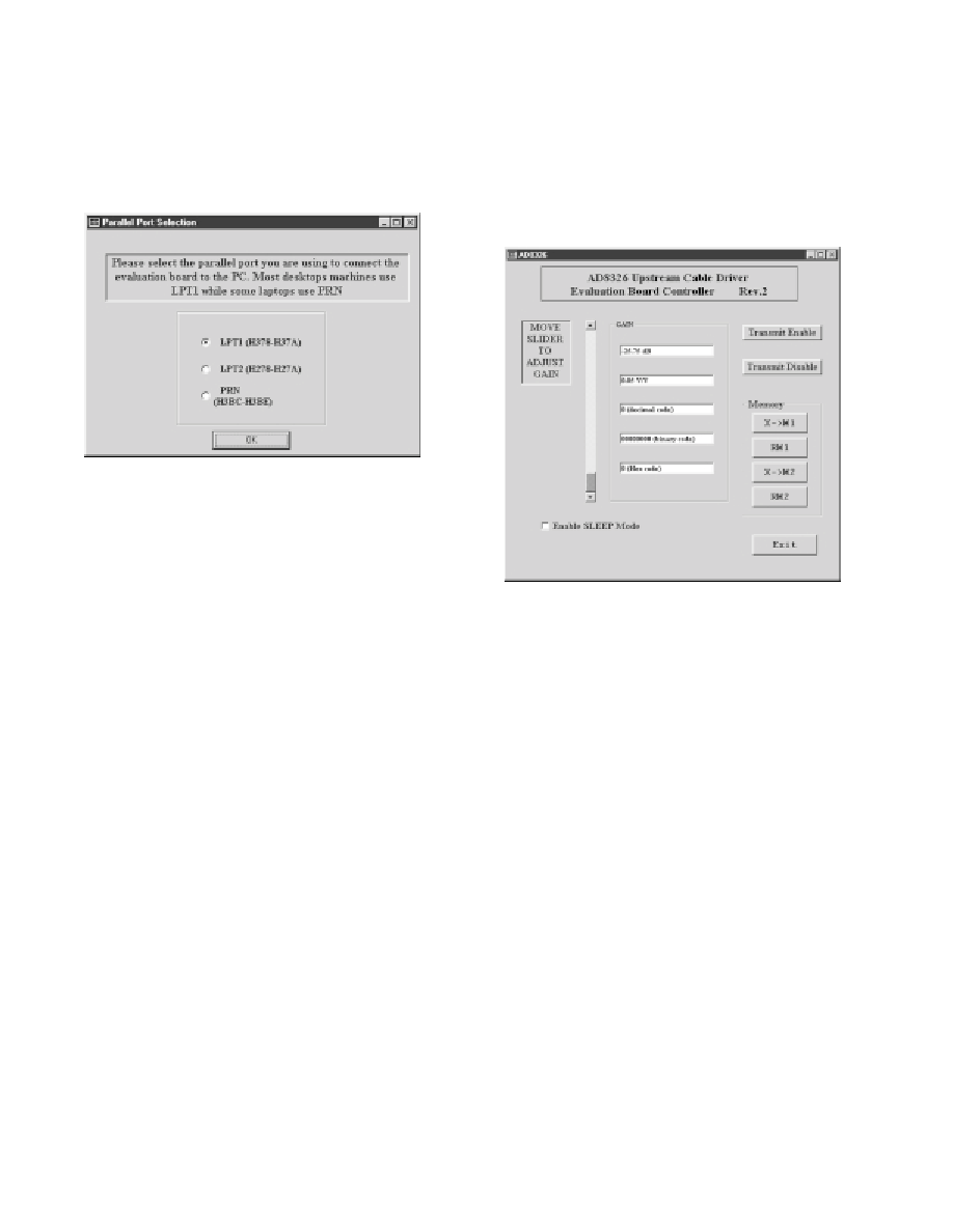
Figure 9. Parallel Port Selection
Controlling Gain/Attenuation of the AD8326
The slide bar controls the gain/attenuation of the AD8326,
which is displayed in dB and in V/V. The gain scales 0.75 dB
per LSB with valid codes from 0 to 71. The gain code from the
position of the slide bar is displayed in decimal, binary, and
hexadecimal (Figure 10).
Transmit Enable and Sleep Mode
The Transmit Enable and Transmit Disable buttons select the
mode of operation of the AD8326 by asserting logic levels on
the asynchronous TXEN pin. The Transmit Disable button
applies Logic 0 to the TXEN pin, disabling forward transmis-
sion while maintaining a 75
back termination. The Transmit
Enable button applies Logic 1 to the TXEN pin, enabling the
AD8326 for forward transmission. Checking the "Enable SLEEP
Mode" checkbox applies logic "0" to the asynchronous
SLEEP
pin, setting the AD8326 for SLEEP mode.
Memory Functions
The MEMORY section of the software provides a way to alter-
nate between two gain settings. The "X->M1" button stores
the current value of the gain slide bar into memory while the
"RM1" button recalls the stored value, returning the gain slide
bar to the stored level. The same applies to the "X->M2" and
"RM2" buttons.
Figure 10. Control Software Interface
REV. 0
AD8326
≠15≠
V
IN
≠
0
V
IN
+ 0
C22
0.1
F
C23
0.1
F
TP13
R15
DNI
R12
78.7
R16
DNI
R14
0
R13
0
R10
DNI
R11
DNI
T3
T4
TO
K
O
1
ETC1
4
3
6
2
1
4
3
6
2
1
TP14
T
O
K
O
1
ETC1
DNI
R18
0
R17
DNI
CABLE_O
V
CC
V
EE
A
GND
TB1
DATEN
SD
A
T
A
CLK
TXEN
SLEEP
1
2
3
4
5
6
7
8
9
10
11
12
13
14
28
27
26
25
24
23
22
21
20
19
18
17
16
15
C4
0.1
F
C6
0.1
F
C5
0.1
F
P1 1
P1 16
P1 15
P1 14
P1 13
P1 12
P1 11
P1 10
P1 9
P1 8
P1 7
P1 6
P1 5
P1 4
P1 3
P1 2
P1 18
P1 17
P1 19
P1 34
P1 33
P1 32
P1 31
P1 30
P1 29
P1 28
P1 27
P1 26
P1 25
P1 24
P1 23
P1 22
P1 21
P1 20
P1 36
P1 35
W1
TP1
TP2
TP3
TP4
TP5
TP6
W2
R1
0
R3
0
R2
0
C3
DNI
C2
DNI
C1
DNI
+
TP7
TP8
TP9
V
EE
R4
OPEN
R5
OPEN
C19
10
F
C18
0.1
F
C17
0.1
F
C20
0.1
F
C21
0.1
F
C16
0.1
F
C15
0.1
F
C14
0.1
F
C13
0.1
F
C12
0.1
F
C11
0.1
F
C10
0.1
F
C9
0.1
F
C20
0.1
F
C7
10
F
+
TP16
TP17
TP18
TP15
V
CC
T1
T2
TO
K
O
1
ETC1
4
3
4
3
6
2
1
R6
OPEN
R19
0
R9
OPEN
R7
0
R8
0
TP10
TP12
TP11
A
GND
HPP
LPP
CBL
COM
CX6002
1
9
5
3,
10
≠
18
Z1
AD8326
A
GND
6
2
1
A
GND
DNI
HPF_O
Figure 11. Evaluation Board Schematic
REV. 0
AD8326
≠16≠
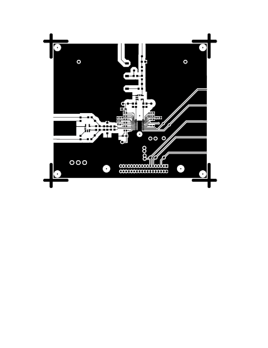
Figure 12. Evaluation Board Layout (Component Side)
REV. 0
AD8326
≠17≠
Figure 13. Evaluation Board Layout (Silkscreen Top)
REV. 0
AD8326
≠18≠
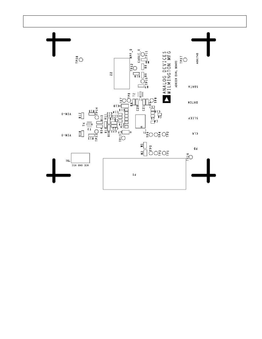
Figure 14. Evaluation Board Layout (Circuit Side)
REV. 0
AD8326
≠19≠
Figure 15. Evaluation Board Layout (Silkscreen Bottom)
REV. 0
AD8326
≠20≠
Figure 16. Evaluation Board Layout (Internal Ground Plane)
REV. 0
AD8326
≠21≠
Figure 17. Evaluation Board Layout (Internal Power Planes)

REV. 0
AD8326
≠22≠
AD8326 Evaluation Board Rev. B ≠ Revised - November 22, 2000
Qty.
Description
Vendor
Ref Description
2
10
µ
F 16 V. B Size Tantalum Chip Capacitor
ADS# 4-7-24
C7, C19
4
0.1
µ
F 50 V. 1206 Size Ceramic Chip Capacitor
ADS# 4-5-18
C20≠23
14
0.1
µ
F 25 V. 603 Size Ceramic Chip Capacitor
ADS# 4-12-8
C4≠C6, C8≠C18
9
0
1/8 W. 1206 Size Chip Resistor
ADS# 3-18- 88
R1≠R3, R7, R8, R13, R14,
R18, R19
1
78.7
1% 1/8 W. 1206 Size Chip Resistor
ADS# 3-18-194
R12
2
Yellow Test Point [INPUTS] (Bisco TP104-01-04)
ADS# 12-18-32
TP13, TP14
6
White Test Point [DATA] (Bisco TP104-0 -09)
ADS# 12-18-42
TP1≠TP6
1
Red Test Point [VCC] (Bisco TP104-01-02)
ADS# 12-18-43
TP15
1
Blue Test Point [VEE] (Bisco TP104-01-06)
ADS# 12-18-62
TP7
3
Black Test Point [AGND] (Bisco TP104-01-00)
ADS# 12-18-44
TP16≠TP18
4
End Launch SMA Connector
ADS# 12-1-31
VIN≠, VIN+, CABLE,
HPF
1
Centronics Type 36 Pin Right-Angle Connector
ADS# 12-3-50
P1
1
3 Terminal Power Block (Green)
ADS# 12-19-14
TB1
1
1:1 Transformer TOKO # 617DB ≠ A0070
TOKO
T3, T1
1
Pulse # CX 6002 Diplexer
PULSE
Z2
1
AD 8326ARE (TSSOP ePad) UPSTREAM Cable Driver
ADI# AD8326XRE
Z1
1
AD 8326ARE REV. B Evaluation PC Board
ADI# AD8326XRE-EVAL
EVAL PCB
4
#4≠40
◊
1/4 Inch STAINLESS Panhead Machine Screw
ADS# 30-1-1
4
#4≠40
◊
3/4 Inch Long Aluminum Round Standoff
ADS# 30-16-3
2
# 2≠56
◊
3/8 inch STAINLESS Panhead Machine Screw
ADS# 30-1-17
(p1 hardware)
2
# 2 Steel Flat Washer
ADS# 30-6-6
(p1 Hardware)
2
# 2 Steel Internal Tooth Lockwasher
ADS# 30-5-2
(p1 Hardware)
2
# 2 STAINLESS STEEL Hex. Machine Nut
ADS# 30-7-6
(p1 Hardware)
Do not install C1≠C3, R4≠R6, R10, R11, R15≠R17, T2, T4, TP8≠TP12, W1≠W2.
REV. 0
AD8326
≠23≠
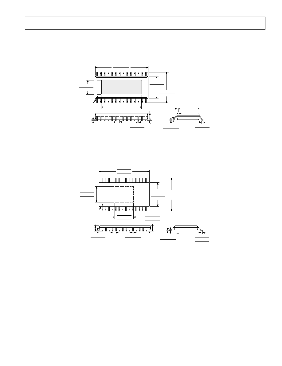
28-Lead PSOP
(RP-28)
28
15
14
1
HEAT SLUG
ON BOTTOM
0.539 (13.69)
0.529 (13.44)
0.711 (18.06)
0.701 (17.81)
0.410 (10.41)
0.400 (10.16)
0.299 (7.59)
0.292 (7.42)
PIN 1
0.189 (4.80)
0.179 (4.55)
0.0125 (0.32)
0.0091 (0.23)
8
0
0.040 (1.27)
0.024 (0.61)
0.016 (0.41)
0.010 (0.25)
45∞
SEATING
PLANE
0.004 (0.10)
0.000 (0.00)
0.019 (0.48)
0.014 (0.36)
0.098 (2.49)
0.090 (2.29)
0.050 (1.27)
BSC
STANDOFF
28-Lead HTSSOP
(RE-28)
0.041 (1.05)
0.039 (1.00)
0.031 (0.80)
SEATING
PLANE
0.047
(1.20)
MAX
0.006 (0.15)
0.000 (0.00)
0.0118 (0.30)
0.0075 (0.19)
0.0256
(0.65)
BSC
0.177 (4.50)
0.173 (4.40)
0.169 (4.30)
28
15
14
1
0.386 (9.80)
0.382 (9.70)
0.378 (9.60)
PIN 1
0.252
(6.40)
BSC
EXPOSED
PAD
ON BOTTOM
0.138 (3.55)
0.136 (3.50)
0.134 (3.45)
0.119 (3.05)
0.117 (3.00)
0.115 (2.95)
0.0079 (0.20)
0.0035 (0.09)
8
0
0.030 (0.75)
0.024 (0.60)
0.177 (0.45)
CONTROLLING DIMENSIONS ARE IN MILLIMETERS (mm)
OUTLINE DIMENSIONS
Dimensions shown in inches and (mm).

≠24≠
C01856≠1.5≠7/01(0)
PRINTED IN U.S.A.