 | –≠–ª–µ–∫—Ç—Ä–æ–Ω–Ω—ã–π –∫–æ–º–ø–æ–Ω–µ–Ω—Ç: AD8353 | –°–∫–∞—á–∞—Ç—å:  PDF PDF  ZIP ZIP |

REV. 0
Information furnished by Analog Devices is believed to be accurate and
reliable. However, no responsibility is assumed by Analog Devices for its
use, nor for any infringements of patents or other rights of third parties that
may result from its use. No license is granted by implication or otherwise
under any patent or patent rights of Analog Devices.
a
AD8353
One Technology Way, P.O. Box 9106, Norwood, MA 02062-9106, U.S.A.
Tel: 781/329-4700
www.analog.com
Fax: 781/326-8703
© Analog Devices, Inc., 2002
100 MHz≠2.7 GHz
RF Gain Block
FUNCTIONAL BLOCK DIAGRAM
BIAS AND VREF
COM1
INPT
VOUT
VPOS
COM2
AD8353
FEATURES
Fixed Gain of 20 dB
Operational Frequency of 100 MHz to 2.7 GHz
Linear Output Power Up to 9 dBm
Input/Output Internally Matched to 50
Temperature and Power Supply Stable
Noise Figure 5.3 dB
Power Supply 3 V or 5 V
APPLICATIONS
VCO Buffers
General Tx/Rx Amplification
Power Amplifier Predriver
Low Power Antenna Driver
PRODUCT DESCRIPTION
The AD8353 is a broadband, fixed-gain linear amplifier that
operates at frequencies from 100 MHz up to 2.7 GHz. It is
intended for use in a wide variety of wireless devices including
cellular, broadband, CATV, and LMDS/MMDS applications.
By taking advantage of Analog Devices' high-performance
complementary Si bipolar process, these gain blocks provide
excellent stability over process, temperature, and power supply.
This amplifier is single-ended and internally matched to 50
with a return loss of greater than 10 dB over the full operating
frequency range.
The AD8353 provides linear output power of 9 dBm with 20 dB
of gain at 900 MHz when biased at 3 V and an external RF
choke is connected between the power supply and the output
pin. The dc supply current is 42 mA. At 900 MHz, the output third
order intercept (OIP3) is greater than 23 dBm, and is 19 dBm
at 2.7 GHz.
The noise figure is 5.3 dB at 900 MHz. The reverse isolation
(S
12
) is ≠36 dB at 900 MHz and ≠30 dB at 2.7 GHz.
The AD8353 can also operate with a 5 V power supply, in which
case no external inductor is required. Under these conditions,
the AD8353 delivers 8 dBm with 20 dB of gain at 900 MHz.
The dc supply current is 42 mA. At 900 MHz, the OIP3 is
greater than 22 dBm and is 19 dBm at 2.7 GHz. The noise
figure is 5.6 dB at 900 MHz. The reverse isolation (S
12
) is ≠35 dB.
The AD8353 is fabricated on Analog Devices' proprietary, high-
performance 25 GHz Si complementary bipolar IC process. The
AD8353 is available in a chip scale package that utilizes an
exposed paddle for excellent thermal impedance and low imped-
ance electrical connection to ground. It operates over a ≠40
∞C
to +85
∞C temperature range.
An evaluation board is available.

REV. 0
≠2≠
AD8353≠SPECIFICATIONS
Parameters
Conditions
Min
Typ
Max
Unit
OVERALL FUNCTION
Frequency Range
0.1
2.7
GHz
Gain
f = 900 MHz
19.8
dB
f = 1.9 GHz
17.7
dB
f = 2.7 GHz
15.6
dB
Delta Gain
f = 900 MHz, ≠40
∞C T
A
+85
∞C
≠0.97
dB
f = 1.9 GHz, ≠40
∞C T
A
+85
∞C
≠1.15
dB
f = 2.7 GHz, ≠40
∞C T
A
+85
∞C
≠1.34
dB
Gain Supply Sensitivity
VPOS
± 10%, f = 900 MHz
0.04
dB/V
f = 1.9 GHz
≠0.004
dB/V
f = 2.7 GHz
≠0.04
dB/V
Reverse Isolation (S
12
)
f = 900 MHz
≠35.6
dB
f = 1.9 GHz
≠34.9
dB
f = 2.7 GHz
≠30.3
dB
RF INPUT INTERFACE
Pin RFIN
Input Return Loss
f = 900 MHz
22.3
dB
f = 1.9 GHz
20.9
dB
f = 2.7 GHz
11.2
dB
RF OUTPUT INTERFACE
Pin VOUT
Output Compression Point
f = 900 MHz, 1 dB compression
9.1
dBm
f = 1.9 GHz
8.4
dBm
f = 2.7 GHz
7.6
dBm
Delta Compression Point
f = 900 MHz, ≠40
∞C T
A
+85
∞C
≠1.46
dB
f = 1.9 GHz, ≠40
∞C T
A
+85
∞C
≠1.17
dB
f = 2.7 GHz, ≠40
∞C T
A
+85
∞C
≠1
dB
Output Return Loss
f = 900 MHz
26.3
dB
f = 1.9 GHz
16.9
dB
f = 2.7 GHz
13.3
dB
DISTORTION/NOISE
Output Third Order Intercept
f = 900 MHz, f = 1 MHz, P
IN
= ≠28 dBm
23.6
dBm
f = 1.9 GHz, f = 1 MHz, P
IN
= ≠28 dBm
20.8
dBm
f = 2.7 GHz, f = 1 MHz, P
IN
= ≠28 dBm
19.5
dBm
Output Second Order Intercept
f = 900 MHz, f = 1 MHz, P
IN
= ≠28 dBm
31.6
dBm
Noise Figure
f = 900 MHz
5.3
dB
f = 1.9 GHz
6
dB
f = 2.7 GHz
6.8
dB
POWER INTERFACE
Pin VPOS
Supply Voltage
2.7
3
3.3
V
Total Supply Current
35
41
48
mA
Supply Voltage Sensitivity
15.3
mA/V
Temperature Sensitivity
≠40
∞C T
A
+85
∞C
60
A/
∞C
(V
S
= 3 V, T
A
= 25 C, 100 nH external inductor between VOUT and VPOS, Z
O
= 50 ,
unless otherwise noted.)
Specifications subject to change without notice.

REV. 0
≠3≠
AD8353
SPECIFICATIONS
(V
S
= 5 V, T
A
= 25 C, no external inductor between VOUT and VPOS, Z
O
= 50 , unless otherwise noted.)
Parameters
Conditions
Min
Typ
Max
Unit
OVERALL FUNCTION
Frequency Range
0.1
2.7
GHz
Gain
f = 900 MHz
19.5
dB
f = 1.9 GHz
17.6
dB
f = 2.7 GHz
15.7
dB
Delta Gain
f = 900 MHz, ≠40
∞C T
A
+85
∞C
≠0.96
dB
f = 1.9 GHz, ≠40
∞C T
A
+85
∞C
≠1.18
dB
f = 2.7 GHz, ≠40
∞C T
A
+85
∞C
≠1.38
dB
Gain Supply Sensitivity
VPOS
± 10%, f = 900 MHz
0.09
dB/V
f = 1.9 GHz
≠0.01
dB/V
f = 2.7 GHz
≠0.09
dB/V
Reverse Isolation (S
12
)
f = 900 MHz
≠35.4
dB
f = 1.9 GHz
≠34.6
dB
f = 2.7 GHz
≠30.2
dB
RF INPUT INTERFACE
Pin RFIN
Input Return Loss
f = 900 MHz
22.9
dB
f = 1.9 GHz
21.7
dB
f = 2.7 GHz
11.5
dB
RF OUTPUT INTERFACE
Pin VOUT
Output Compression Point
f = 900 MHz
8.3
dBm
f = 1.9 GHz
8.1
dBm
f = 2.7 GHz
7.5
dBm
Delta Compression Point
f = 900 MHz, ≠40
∞C T
A
+85
∞C
≠1.05
dB
f = 1.9 GHz, ≠40
∞C T
A
+85
∞C
≠1.49
dB
f = 2.7 GHz, ≠40
∞C T
A
+85
∞C
≠1.33
dB
Output Return Loss
f = 900 MHz
27
dB
f = 1.9 GHz
22
dB
f = 2.7 GHz
14.3
dB
DISTORTION/NOISE
Output Third Order Intercept
f = 900 MHz, f = 1 MHz, P
IN
= ≠28 dBm
22.8
dBm
f = 1.9 GHz, f = 1 MHz, P
IN
= ≠28 dBm
20.6
dBm
f = 2.7 GHz, f = 1 MHz, P
IN
= ≠28 dBm
19.5
dBm
Output Second Order Intercept
f = 900 MHz, f = 1 MHz, P
IN
= ≠28 dBm
30.3
dBm
Noise Figure
f = 900 MHz
5.6
dB
f = 1.9 GHz
6.3
dB
f = 2.7 GHz
7.1
dB
POWER INTERFACE
Pin VPOS
Supply Voltage
4.5
5
5.5
V
Total Supply Current
35
42
52
mA
Supply Voltage Sensitivity
4.3
mA/V
Temperature Sensitivity
≠40
∞C T
A
+85
∞C
45.7
A/
∞C
Specifications subject to change without notice.
REV. 0
AD8353
≠4≠
ABSOLUTE MAXIMUM RATINGS
*
Supply Voltage VPOS . . . . . . . . . . . . . . . . . . . . . . . . . . 5.5 V
Input Power (re: 50
) . . . . . . . . . . . . . . . . . . . . . . . 10 dBm
Equivalent Voltage . . . . . . . . . . . . . . . . . . . . . . 700 mV rms
Internal Power Dissipation
Paddle Not Soldered . . . . . . . . . . . . . . . . . . . . . . . 325 mW
Paddle Soldered . . . . . . . . . . . . . . . . . . . . . . . . . . . 812 mW
JA
(Paddle Soldered) . . . . . . . . . . . . . . . . . . . . . . . . . 80
∞C/W
JA
(Paddle Not Soldered) . . . . . . . . . . . . . . . . . . . . 200
∞C/W
Maximum Junction Temperature . . . . . . . . . . . . . . . . 150
∞C
Operating Temperature Range . . . . . . . . . . . ≠40
∞C to +85∞C
Storage Temperature Range . . . . . . . . . . . . ≠65
∞C to +150∞C
Lead Temperature Range (Soldering 60 sec) . . . . . . . . 240
∞C
*Stresses above those listed under Absolute Maximum Ratings may cause perma-
nent damage to the device. This is a stress rating only; functional operation of the
device at these or any other conditions above those indicated in the operational
section of this specification is not implied. Exposure to absolute maximum rating
conditions for extended periods may affect device reliability.
CAUTION
ESD (electrostatic discharge) sensitive device. Electrostatic charges as high as 4000 V readily
accumulate on the human body and test equipment and can discharge without detection. Although
the AD8353 features proprietary ESD protection circuitry, permanent damage may occur on
devices subjected to high-energy electrostatic discharges. Therefore, proper ESD precautions are
recommended to avoid performance degradation or loss of functionality.
WARNING!
ESD SENSITIVE DEVICE
PIN FUNCTION DESCRIPTIONS
Pin
Mnemonic Description
1, 8
COM1
Device Common.
Connect to low
impedance ground.
3
INPT
RF Input Connection.
Must be ac-coupled.
4, 5
COM2
Device Common.
Connect to low
impedance ground.
6
VPOS
Positive Supply Voltage
2
NC
No Connection
7
VOUT
RF Output Connection.
Must be ac-coupled.
ORDERING GUIDE
Temperature
Package
Package
Model
Range
Description
Option
AD8353ACP≠REEL7 ≠40
∞C to +85∞C 7" Tape and Reel CP-8
AD8353≠EVAL
Evaluation Board
PIN CONFIGURATION
TOP VIEW
(Not to Scale)
8
7
6
5
1
2
3
4
NC = NO CONNECT
COM1
NC
INPT
COM1
VOUT
VPOS
COM2
COM2
AD8353
REV. 0
≠5≠
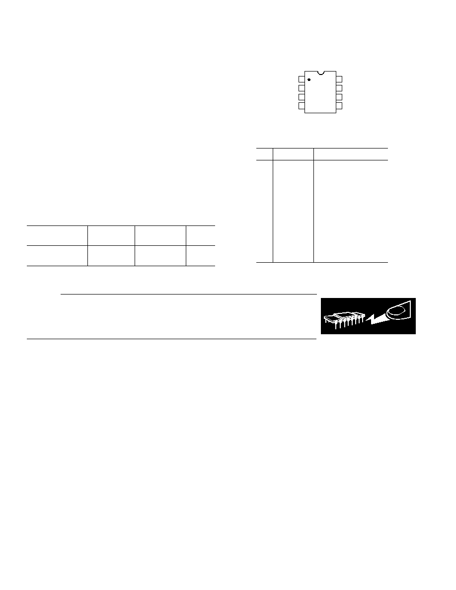
AD8353
180
150
120
90
60
30
0
330
300
270
240
210
TPC 1. S
11
vs. Frequency, V
S
= 3 V, T
A
= 25 C,
100 MHz
f 3 GHz
FREQUENCY ≠ MHz
25
500
1000
1500
2000
3000
GAIN ≠ dB
20
15
10
5
0
2500
GAIN AT 3.0V
GAIN AT 3.3V
GAIN AT 2.7V
0
TPC 2. Gain vs. Frequency, V
S
= 2.7 V, 3 V, and 3.3 V,
T
A
= 25 C
FREQUENCY ≠ MHz
500
1000
1500
3000
REVERSE ISOLA
T
ION
≠
dB
S
12
AT 3.0V
S
12
AT 3.3V
S
12
AT 2.7V
2500
2000
0
0
≠20
≠30
≠10
≠15
≠25
≠5
≠35
≠40
TPC 3. Reverse Isolation vs. Frequency,
V
S
= 2.7 V, 3 V,
and 3.3 V, T
A
= 25 C
180
150
120
90
60
30
0
330
300
270
240
210
TPC 4. S
22
vs. Frequency, V
S
= 3 V, T
A
= 25 C,
100 MHz
f 3 GHz
FREQUENCY ≠ MHz
25
500
1000
1500
2000
2500
GAIN
≠
dB
15
10
5
0
3000
20
GAIN AT ≠40 C
GAIN AT +85 C
GAIN AT +25 C
0
TPC 5. Gain vs. Frequency, V
S
= 3 V, T
A
= ≠40 C, +25 C,
and +85 C
FREQUENCY ≠ MHz
0
500
1000
1500
3000
REVERSE ISOLA
T
ION
≠
dB
≠20
≠30
≠10
≠15
≠25
≠5
S
12
AT ≠40 C
S
12
AT +85 C
2500
2000
0
S
12
AT +25 C
≠35
≠40
TPC 6. Reverse Isolation vs. Frequency,
V
S
= 3 V,
T
A
= ≠40 C, +25 C, and +85 C
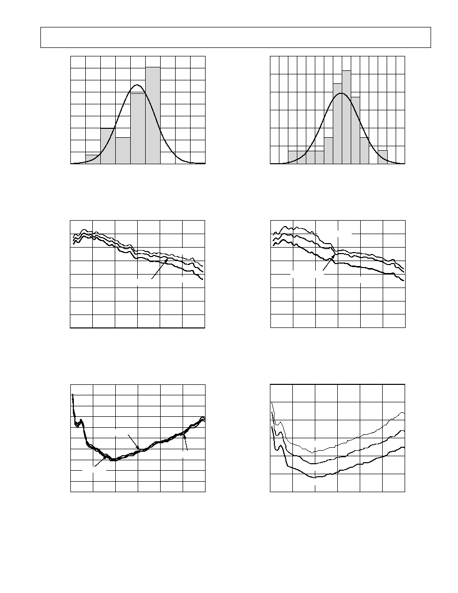
Typical Performance Characteristics≠
REV. 0
AD8353
≠6≠
FREQUENCY ≠ MHz
500
1000
1500
2000
2500
P
1
dB
≠
dBm
10
6
4
2
3000
12
8
0
P
1
dB
AT 3.3V
P
1
dB
AT 3.0V
P
1
dB
AT 2.7V
0
TPC 7. P
1 dB
vs. Frequency, V
S
= 2.7 V, 3 V, and 3.3 V,
T
A
= 25 C
OUTPUT 1 dB COMPRESSION POINT ≠ dBm
7.0
7.2
PERCENT
A
G
E
≠
%
35
10
45
25
0
40
20
15
30
5
7.4
7.6
7.8
8.0
8.2
8.4
8.6
8.8
9.0
TPC 8. Distribution of P
1 dB
V
S
= 3 V, T
A
= 25 C,
f = 2.2 GHz
FREQUENCY ≠ MHz
500
1000
1500
2000
2500
OIP3
≠
dBm
26
16
14
12
3000
28
20
10
22
18
24
OIP3 AT 3.3V
OIP3 AT 3.0V
OIP3 AT 2.7V
0
TPC 9. OIP3 vs. Frequency, V
S
= 2.7 V, 3 V, and 3.3 V,
T
A
= 25 C
FREQUENCY ≠ MHz
500
1000
1500
2000
2500
3000
P
1
dB
≠
dBm
10
6
4
2
12
8
0
P
1
dB
AT ≠40 C
P
1
dB
AT +25 C
P
1
dB
AT +85 C
0
TPC 10. P
1 dB
vs. Frequency, V
S
= 3 V, T
A
= ≠40 C, +25 C,
and +85 C
OIP3 ≠ dBm
19.1
PERCENT
A
G
E
≠
%
30
0
25
15
10
20
5
19.5
19.9
20.3
20.7
21.1
21.5
21.9
TPC 11. Distribution of OIP3, V
S
= 3 V,
T
A
= 25 C,
f = 2.2 GHz
FREQUENCY ≠ MHz
500
1000
1500
2000
2500
OIP3
≠
dBm
26
16
14
12
3000
28
20
10
22
18
24
OIP3 AT +85 C
OIP3 AT ≠40 C
OIP3 AT +25 C
0
TPC 12. OIP3 vs. Frequency, V
S
= 3 V, T
A
= ≠40 C, +25 C,
and +85 C
REV. 0
≠7≠
AD8353
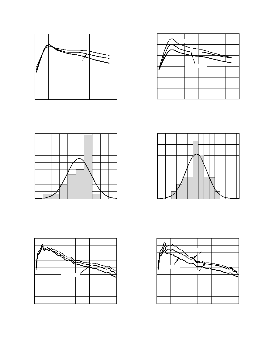
FREQUENCY ≠ MHz
500
1000
1500
2000
2500
NOISE FIGURE
≠
dB
5.5
5.0
4.5
3000
8.0
6.5
4.0
7.0
6.0
7.5
NF AT 3.3V
NF AT 3.0V
NF AT 2.7V
0
TPC 13. Noise Figure vs. Frequency,
V
S
= 2.7 V, 3 V,
and 3.3 V, T
A
= 25 C
NOISE FIGURE ≠ dB
5.90 5.95
PERCENT
A
G
E
≠
%
10
45
25
0
40
20
15
5
6.00
6.10 6.15
6.30 6.35
6.45 6.50 6.55
6.20 6.25
6.40
6.60
6.05
TPC 14. Distribution of Noise Figure, V
S
= 3 V,
T
A
= 25 C, f = 2.2 GHz
180
150
120
90
60
30
0
330
300
270
240
210
TPC 15.
S
11
vs. Frequency, V
S
= 5 V, T
A
= 25
∞C,
100 MHz
f 3 GHz
FREQUENCY ≠ MHz
500
1000
1500
2000
2500
NOISE FIGURE
≠
dB
5.5
5.0
4.5
3000
8.5
6.5
4.0
7.0
6.0
7.5
8.0
NF AT ≠40 C
NF AT +25 C
NF AT +85 C
0
TPC 16. Noise Figure vs. Frequency, V
S
= 3 V,
T
A
= ≠40
∞C, +25∞C, and +85∞C
TEMPERATURE ≠ C
≠60
SUPPL
Y CURRENT
≠
mA
10
50
40
0
45
30
15
5
0
40
35
25
20
I
S
AT 3.0V
I
S
AT 3.3V
I
S
AT 2.7V
≠40
20
60
80
≠20
100
TPC 17. Supply Current vs. Temperature,
V
S
= 2.7 V,
3 V, and 3.3 V
180
150
120
90
60
30
0
330
300
270
240
210
TPC 18.
S
22
vs. Frequency, V
S
= 5 V, T
A
= 25
∞C,
100 MHz
f 3 GHz

REV. 0
AD8353
≠8≠
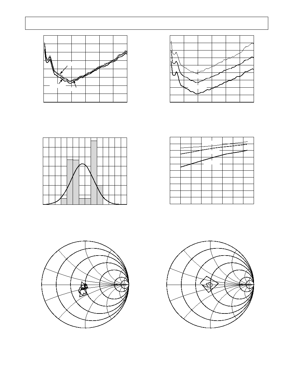
FREQUENCY ≠ MHz
500
1000
1500
GAIN
≠
dB
15
10
5
25
20
0
GAIN AT 5.0V
GAIN AT 4.5V
GAIN AT 5.5V
2000
3000
2500
0
TPC 19. Gain vs. Frequency, V
S
= 4.5 V, 5 V, and
5.5 V, T
A
= 25 C
FREQUENCY ≠ MHz
500
1000
1500
2000
2500
REVERSE ISOLA
T
ION
≠
dB
≠20
≠30
≠35
3000
0
≠10
≠40
≠15
≠25
≠5
S
12
AT 5V
S
12
AT 4.5V
S
12
AT 5.5V
0
TPC 20. Reverse Isolation vs. Frequency, V
S
= 4.5 V,
5 V, and 5.5 V, T
A
= 25 C
FREQUENCY ≠ MHz
500
1000
1500
2000
2500
5
3
1
3000
10
9
0
7
4
2
6
8
P
1
dB
AT 5.0V
P
1
dB
AT 4.5V
P
1
dB
AT 5.5V
0
P
1
dB
≠
dBm
TPC 21. P
1 dB
vs. Frequency, V
S
= 4.5 V,
5 V,
and 5.5 V, T
A
= 25 C
FREQUENCY ≠ MHz
500
1000
1500
GAIN
≠
dB
15
10
5
25
20
0
2000
2500
3000
0
GAIN AT ≠40 C
GAIN AT +25 C
GAIN AT +85 C
TPC 22. Gain vs. Frequency, V
S
= 5 V, T
A
= ≠40
∞C,
+25 C, and +85 C
500
1000
1500
REVERSE ISOLA
T
ION
≠
dB
≠15
≠25
0
≠5
2000
≠10
≠20
≠30
S
12
AT ≠40 C
S
12
AT +25 C
S
12
AT +85 C
2500
3000
0
FREQUENCY ≠ MHz
≠35
≠40
TPC 23. Reverse Isolation vs. Frequency, V
S
= 5 V,
T
A
= ≠40 C, +25 C, and +85 C
FREQUENCY ≠ MHz
500
1000
1500
2000
2500
10
6
2
3000
12
0
8
4
P
1
dB
AT ≠40 C
P
1
dB
AT +85 C
P
1
dB
AT +25 C
0
P
1
dB
≠
dBm
TPC 24. P
1 dB
vs. Frequency, V
S
= 5 V,
T
A
= ≠40 C,
+25 C, and +85 C
REV. 0
≠9≠
AD8353
OUTPUT 1 dB COMPRESSION POINT ≠ dBm
7.0
7.2
PERCENT
A
G
E
≠
%
10
45
35
0
40
30
20
5
7.4
7.8
8.2
8.4
8.6
8.0
8.8
7.6
15
25
TPC 25. Distribution of P
1 dB
, V
S
= 3 V, T
A
= 25
∞C,
f = 2.2 GHz
FREQUENCY ≠ MHz
500
1000
1500
2000
2500
OIP3
≠
dBm
20
16
12
3000
26
24
10
18
14
22
OIP3 AT 5.5V
OIP3 AT 5.0V
OIP3 AT 4.5V
0
TPC 26. OIP3 vs. Frequency, V
S
= 4.5 V,
5 V, and
5.5 V, T
A
= 27 C
FREQUENCY ≠ MHz
500
1000
1500
2000
2500
NOISE FIGURE
≠
dB
6.5
5.5
4.5
3000
9.0
8.0
4.0
6.0
5.0
7.0
8.5
7.5
NF AT 4.5V
NF AT 5.5V
NF AT 5.0V
0
TPC 27.
Noise Figure vs. Frequency, V
S
= 4.5 V, 5 V,
and 5.5 V, T
A
= 25 C
OIP3 ≠ dBm
18.8
20.0
PERCENT
A
G
E
≠
%
10
30
0
20
5
20.4
21.2
21.6
20.8
25
15
19.6
19.2
TPC 28. Distribution of OIP3, V
S
= 5 V,
T
A
= 25 C,
f = 2.2 GHz
FREQUENCY ≠ MHz
500
1000
1500
2000
2500
OIP3
≠
dBm
20
16
12
3000
26
24
10
18
14
22
OIP3 AT ≠40 C
OIP3 AT +25 C
OIP3 AT +85 C
0
TPC 29. OIP3 vs. Frequency, V
S
= 5 V,
T
A
= ≠40 C,
+25 C, and +85 C
FREQUENCY ≠ MHz
500
1000
1500
2000
2500
NOISE FIGURE
≠
dB
7
5
3000
10
9
4
8
6
NF AT ≠40 C
NF AT +85 C
NF AT +25 C
0
TPC 30. Noise Figure vs. Frequency, V
S
= 5 V, T
A
= ≠40 C,
+25 C, and +85 C

REV. 0
AD8353
≠10≠
NOISE FIGURE ≠ dB
6.10 6.15
PERCENT
A
G
E
≠
%
10
30
0
25
15
5
6.20 6.25 6.30 6.35
6.45
6.55 6.60 6.65 6.70
6.40
6.50
20
TPC 31. Distribution of Noise Figure, V
S
= 5 V,
T
A
= 25 C, f = 2.2 GHz
TEMPERATURE ≠ C
≠60
0
80
SUPPL
Y CURRENT
≠
mA
25
15
5
100
50
40
0
20
10
30
45
35
I
S
AT 5.0V
I
S
AT 5.5V
I
S
AT 4.5V
60
40
20
≠20
≠40
TPC 32. Supply Current vs. Temperature,
V
S
= 4.5 V,
5 V, and 5.5 V
P
IN
≠ dBm
15
≠15
≠30
5
≠25
P
OUT
≠
dBm
≠20
≠15
≠10
≠5
0
10
5
0
≠5
≠10
20
14
19
18
17
16
15
GAIN
≠
dB
TPC 33. Output Power and Gain vs. Input Power,
V
S
= 3 V, T
A
= 25∫C, f = 900 MHz
P
IN
≠ dBm
15
≠15
≠30
5
≠25
P
OUT
≠
dBm
≠20
≠15
≠10
≠5
0
10
5
0
≠5
≠10
20
14
19
18
17
16
15
GAIN
≠
dB
TPC 34. Output Power and Gain vs. Input Power,
V
S
= 5 V, T
A
= 25∫C, f = 900 MHz
REV. 0
AD8353
≠11≠
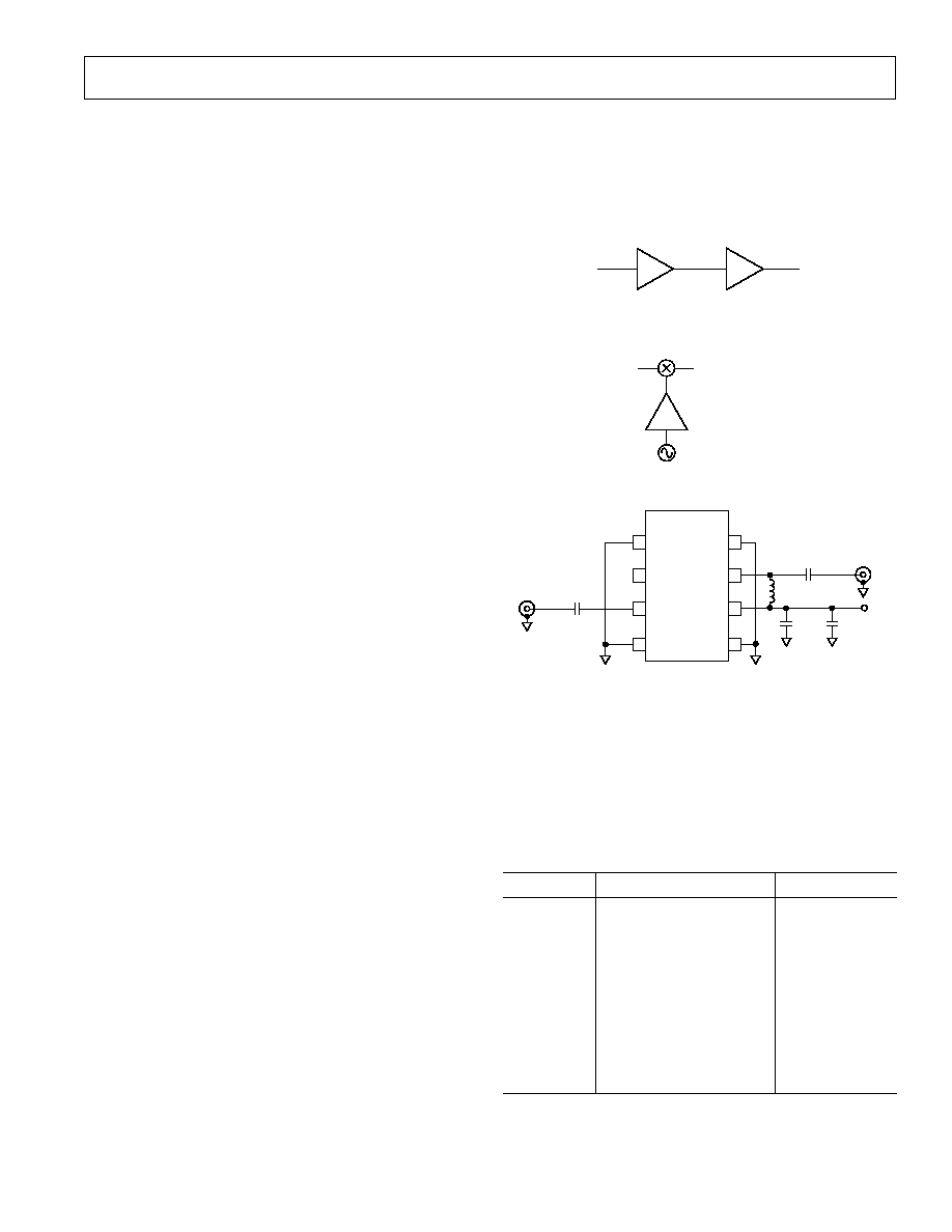
THEORY OF OPERATION
The AD8353 is a two-stage feedback amplifier employing both
shunt-series and shunt-shunt feedback. The first stage is degen-
erated and resistively loaded, and provides approximately 10 dB
of gain. The second stage is a PNP-NPN Darlington output
stage, which provides another 10 dB of gain. Series-shunt feed-
back from the emitter of the output transistor sets the input
impedance to 50
over a broad frequency range. Shunt-shunt
feedback from the amplifier output to the input of the Darlington
stage helps to set the output impedance to 50
. The amplifier
can be operated from a 3 V supply by adding a choke inductor
from the amplifier output to VPOS. Without this choke induc-
tor, operation from a 5 V supply is also possible.
BASIC CONNECTIONS
The AD8353 RF Gain Block is a fixed-gain amplifier with
single-ended input and output ports whose impedances are
nominally equal to 50
over the frequency range 100 MHz to
2.7 GHz. Consequently, it can be directly inserted into a 50
system with no impedance-matching circuitry required. The input
and output impedances are sufficiently stable versus variations
in temperature and supply voltage that no impedance matching
compensation is required. A complete set of scattering parameters
is available at the Analog Devices website (www.analog.com).
The input pin (INPT) is connected directly to the base of the
first amplifier stage, which is internally biased to approximately 1 V,
so a dc-blocking capacitor should be connected between the
source that drives the AD8353 and the input pin, INPT.
It is critical to supply very low inductance ground connections
to the ground pins (pins 1, 4, 5, and 8) as well as to the back-
side exposed paddle. This will ensure stable operation.
The AD8353 is designed to operate over a wide supply voltage
range, from 2.7 V to 5.5 V. The output of the part, VOUT, is
taken directly from the collector of the output amplifier stage.
This node is internally biased to approximately 2.2 V when the
supply voltage is 5 V. Consequently, a dc-blocking capacitor
should be connected between the output pin, VOUT, and the
load that it drives. The value of this capacitor is not critical, but
it should be 100 pF or larger.
When the supply voltage is 3 V, it is recommended that an
external RF choke be connected between the supply voltage and
the output pin, VOUT. This will increase the dc voltage applied
to the collector of the output amplifier stage, which will improve
performance of the AD8353 to be very similar to the performance
produced when 5 V is used for the supply voltage. The inductance
of the RF choke should be approximately 100 nH, and care should
be taken to ensure that the lowest series self-resonant frequency
of this choke is well above the maximum frequency of operation
for the AD8353.
The supply voltage input, VPOS, should be bypassed using a
large value capacitance (approximately 0.47
µF or larger) and a
smaller, high-frequency bypass capacitor (approximately 100 pF)
physically located close to the VPOS pin.
The recommended connections and components are shown in
the schematic of the AD8353 evaluation board.
APPLICATIONS
The AD8353 RF Gain Block may be used as a general purpose
fixed-gain amplifier in a wide variety of applications, such as a
driver for a transmitter power amplifier (Figure 1). Its excellent
reverse isolation also makes this amplifier suitable for use as a
local oscillator buffer amplifier that would drive the local oscilla-
tor port of an up or down converter mixer (Figure 2).
AD8353
HIGH POWER
AMPLIFIER
Figure 1. AD8353 as a Driver Amplifier
MIXER
AD8353
LOCAL
OSCILLATOR
Figure 2. AD8353 as a LO Driver Amplifier
NC = NO CONNECT
COM1
NC
INPT
COM1
VOUT
VPOS
COM2
COM2
AD8353
C3
100pF
C4
0.47 F
VP
OUTPUT
1
2
3
4
5
6
7
8
C2
1000pF
C1
1000pF
INPUT
L1
Figure 3. Evaluation Board Schematic
EVALUATION BOARD
Figure 3 shows the schematic of the AD8353 evaluation board.
Note that L1 is shown as an optional component that is used to
obtain maximum gain only when V
P
= 3 V. The board is powered
by a single supply in the range 2.7 V to 5.5 V. The power supply
is decoupled by a 0.47
µF and a 100 pF capacitor.
Table I. Evaluation Board Configuration Options
Component
Function
Default Value
C1, C2
AC-Coupling Capacitors
1000 pF, 0603
C3
High-Frequency Bypass
Capacitor
100 pF, 0603
C4
Low-Frequency Bypass
Capacitor
0.47
µF, 0603
L1
Optional RF Choke,
used to increase current
through output stage
when V
P
= 3 V.
Not recommended for use
when V
P
= 5 V.
100 nH, 0603
REV. 0
≠12≠
C02721≠0≠2/02(0)
PRINTED IN U.S.A.
AD8353
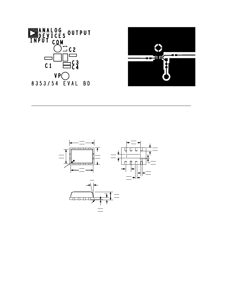
8-Lead LFCSP
(CP-8)
1.89
1.74
1.59
0.50 BSC
0.30
0.23
0.18
0.60
0.45
0.30
0.55
0.40
0.30
SEATING
PLANE
12
0
0.25 REF
0.05
0.02
0.00
1.00
0.90
0.80
3.25
3.00
2.75
1.95
1.75
1.55
2.95
2.75
2.55
PIN 1
INDICATOR
2.25
2.00
1.75
NOTES
1. CONTROLLING DIMENSIONS ARE IN MILLIMETERS.
2. PADDLE IS COPPER PLATED WITH LEAD FINISH.
0.15
0.10
0.05
0.25
0.20
0.15
BOTTOM VIEW
4
5
8
1
OUTLINE DIMENSIONS
Dimensions shown in millimeters.
Figure 4. Silkscreen Top
Figure 5. Component Side