 | –≠–ª–µ–∫—Ç—Ä–æ–Ω–Ω—ã–π –∫–æ–º–ø–æ–Ω–µ–Ω—Ç: AD8642 | –°–∫–∞—á–∞—Ç—å:  PDF PDF  ZIP ZIP |
Document Outline
- FEATURES
- APPLICATIONS
- GENERAL DESCRIPTION
- TABLE OF CONTENTS
- REVISION HISTORY
- ˛ˇ
- ˛ˇ
- ˛ˇ
- ˛ˇ

Low Power, Rail-to-Rail Output
Precision JFET Amplifier
AD8641/AD8642
Rev. A
Information furnished by Analog Devices is believed to be accurate and reliable.
However, no responsibility is assumed by Analog Devices for its use, nor for any
infringements of patents or other rights of third parties that may result from its use.
Specifications subject to change without notice. No license is granted by implication
or otherwise under any patent or patent rights of Analog Devices. Trademarks and
registered trademarks are the property of their respective owners.
One Technology Way, P.O. Box 9106, Norwood, MA 02062-9106, U.S.A.
Tel: 781.329.4700
www.analog.com
Fax: 781.461.3113
© 2005 Analog Devices, Inc. All rights reserved.
FEATURES
Low supply current: 250 µA max
Very low input bias current: 1 pA max
Low offset voltage: 750 µV max
Single-supply operation: 5 V to 26 V
Dual-supply operation: ±2.5 V to ±13 V
Rail-to-rail output
Unity gain stable
No phase reversal
SC70 package
APPLICATIONS
Line-/battery-powered instruments
Photodiode amplifiers
Precision current sensing
Medical instrumentation
Industrial controls
Precision filters
Portable audio
ATE
OUT
1
+IN
3
VEE
2
VCC
5
≠IN
4
AD8641
TOP VIEW
(Not to Scale)
05072-101
Figure 1. 5-Lead SC70 (KS-5)
NC
1
≠IN
2
+IN
3
VEE
4
NC
8
VCC
7
OUT
6
NC
5
AD8641
TOP VIEW
(Not to Scale)
05072-102
NC = NO CONNECT
Figure 2. 8-Lead SOIC (R-8)
OUT A
1
≠IN A
2
+IN A
3
V≠
4
V+
8
OUT B
7
≠IN B
6
+IN B
5
AD8642
TOP VIEW
(Not to Scale)
05072-063
Figure 3. 8-Lead SOIC (R-8)
OUT A
1
≠IN A
2
+IN A
3
V≠
4
V+
8
OUT B
7
≠IN B
6
+IN B
5
AD8642
TOP VIEW
(Not to Scale)
05072-064
Figure 4. 8-Lead MSOP (RM-8)
GENERAL DESCRIPTION
The AD8641/AD8642 are low power, precision JFET input
amplifiers featuring extremely low input bias current and rail-
to-rail output. The ability to swing nearly rail-to-rail at the
input and rail-to-rail at the output enables designers to buffer
CMOS DACs, ASICs, and other wide output swing devices in
single-supply systems. The outputs remain stable with
capacitive loads of more than 500 pF.
The AD8641/AD8642 are suitable for applications utilizing
multichannel boards that require low power to manage heat.
Other applications include photodiodes, ATE reference level
drivers, battery management, and industrial controls.
The AD8641/AD8642 are fully specified over the extended
industrial temperature range of ≠40∞C to +125∞C. The AD8641
is available in 5-lead SC70 and 8-lead SOIC lead-free packages.
The AD8642 is available in 8-lead MSOP and 8-lead SOIC lead-
free packages.

AD8641/AD8642
Rev. A | Page 2 of 16
TABLE OF CONTENTS
Specifications..................................................................................... 3
Electrical Characteristics............................................................. 3
Absolute Maximum Ratings............................................................ 5
Typical Performance Characteristics ............................................. 6
Outline Dimensions ....................................................................... 13
Ordering Guide........................................................................... 14
REVISION HISTORY
3/05--Rev. 0 to Rev. A
Added AD8642 ...................................................................Universal
Changes to General Description .................................................... 1
Added Figure 3 and Figure 4........................................................... 1
Changes to Specifications ................................................................ 3
Changes to Absolute Maximum Ratings ....................................... 5
Changes to Figure 22........................................................................ 8
Changes to Figure 23........................................................................ 9
Changes to Figure 41...................................................................... 12
Updated Outline Dimensions ....................................................... 13
Changes to Ordering Guide .......................................................... 14
10/04--Initial Version: Revision 0

AD8641/AD8642
Rev. A | Page 3 of 16
SPECIFICATIONS
ELECTRICAL CHARACTERISTICS
@ V
S
= 5.0 V, V
CM
= 2.5 V, T
A
= 25∞C, unless otherwise noted.
Table 1.
Parameter
Symbol
Conditions
Min
Typ
Max
Unit
INPUT CHARACTERISTICS
Offset Voltage
V
OS
50
750
µV
≠40∞C < T
A
< +85∞C
1.5
mV
+85∞C < T
A
< +125∞C, V
CM
= 1.5 V
1.6
mV
Input Bias Current
I
B
0.25
1
pA
≠40∞C < T
A
< +125∞C
180
pA
Input Offset Current
I
OS
0.5
pA
≠40∞C < T
A
< +125∞C
60
pA
Input Voltage Range
0
3
V
Common-Mode Rejection Ratio
CMRR
V
CM
= 0 V to 2.5 V
74
93
dB
Large Signal Voltage Gain
A
VO
R
L
= 10 k, V
O
= 0.5 to 4.5 V
80
140
V/mV
Offset Voltage Drift
V
OS
/T
≠40∞C < T
A
< +125∞C
2.5
µV/∞C
OUTPUT CHARACTERISTICS
Output Voltage High
V
OH
4.95
V
I
L
= 1 mA, ≠40∞C to +125∞C
4.94
V
Output Voltage Low
V
OL
0.05
V
I
L
= 1 mA, ≠40∞C to +125∞C
0.01
0.05
V
Output Current
I
OUT
±6
mA
POWER
SUPPLY
Power Supply Rejection Ratio
PSRR
V
S
= 5 V to 26 V
90
107
dB
Supply Current/Amplifier
I
SY
195
250
µA
≠40∞C < T
A
< +125∞C
270
µA
DYNAMIC PERFORMANCE
Slew Rate
SR
2
V/µs
Gain Bandwidth Product
GBP
3
MHz
Phase Margin
ÿ
O
50
Degrees
NOISE PERFORMANCE
Voltage Noise
e
N
p-p
f = 0.1 Hz to 10 Hz
4.0
µV p-p
Voltage Noise Density
e
N
f = 1 kHz
28.5
nV/Hz
Current Noise Density
i
N
f = 1 kHz
0.5
fA/Hz

AD8641/AD8642
Rev. A | Page 4 of 16
@ V
S
= ±13 V, V
CM
= 0 V, T
A
=25∞C, unless otherwise noted.
Table 2.
Parameter
Symbol
Conditions
Min
Typ
Max
Unit
INPUT CHARACTERISTICS
Offset Voltage
V
OS
70
750
µV
≠40∞ < T
A
< +125∞C
1.5
mV
Input Bias Current
I
B
0.25
1
pA
≠40∞C < T
A
< +125∞C
260
pA
Input Offset Current
I
OS
0.5
pA
≠40∞C < T
A
< +125∞C
65
pA
Input Voltage Range
≠13
+10
V
Common-Mode Rejection Ratio
CMRR
V
CM
= -13 V to +10 V
90
107
dB
Large Signal Voltage Gain
A
VO
R
L
= 10 k, V
O
= ≠11 V to +11 V
215
290
V/mV
Offset Voltage Drift
V
OS
/T
≠40∞C < T
A
< +125∞C
2.5
µV/∞C
OUTPUT CHARACTERISTICS
Output Voltage High
V
OH
+12.95
V
I
L
= 1 mA, ≠40∞C to +125∞C
+12.94
V
Output Voltage Low
V
OL
≠12.95
V
I
L
= 1 mA, ≠40∞C to +125∞C
≠12.94
V
Output Current
I
OUT
±12
mA
POWER SUPPLY
Power Supply Rejection Ratio
PSRR
V
S
= ±2.5 V to ±13 V
90
107
dB
Supply Current/Amplifier
I
SY
200
290
µA
≠40∞C < T
A
< +125∞C
330
µA
DYNAMIC PERFORMANCE
Slew Rate
SR
3
V/µs
Gain Bandwidth Product
GBP
3.5
MHz
Phase Margin
ÿ
O
60
Degrees
NOISE PERFORMANCE
Voltage Noise
e
N
p-p
f = 0.1 Hz to 10 Hz
4.2
µV p-p
Voltage Noise Density
e
N
f = 1 kHz
27.5
nV/Hz
Current Noise Density
i
N
f = 1 kHz
0.5
fA/Hz
AD8641/AD8642
Rev. A | Page 5 of 16
ABSOLUTE MAXIMUM RATINGS
Table 3.
1
Parameter Rating
Supply Voltage
27.3 V
Input Voltage
VS≠ to VS+
Differential Input Voltage
±Supply Voltage
Output Short-Circuit Duration Indefinite
Storage Temperature Range
KS-5, R-8, RM-8 Packages
≠65∞C to +150∞C
Operating Temperature Range
≠40∞C to +125∞C
Junction Temperature Range
KS-5, R-8, RM-8 Packages
≠65∞C to +150∞C
Lead Temperature Range (Soldering, 60 Sec)
300∞C
Stresses above those listed under Absolute Maximum Ratings
may cause permanent damage to the device. This is a stress
rating only; functional operation of the device at these or any
other conditions above those listed in the operational sections
of this specification is not implied. Exposure to absolute
maximum rating conditions for extended periods may affect
device reliability.
Table 4.
Package Type
JA
2
JC
Unit
5-Lead SC70 (KS-5)
331.4
223.9
∞C/W
8-Lead SOIC (R-8)
157
56
∞C/W
8-Lead MSOP (RM-8)
206
44
∞C/W
1
Absolute maximum ratings apply at 25∞C, unless otherwise noted.
2
JA
is specified for the worst-case conditions, i.e.,
JA
is specified for devices
soldered on circuit boards for surface-mounted packages.
ESD CAUTION
ESD (electrostatic discharge) sensitive device. Electrostatic charges as high as 4000 V readily accumulate on
the human body and test equipment and can discharge without detection. Although this product features
proprietary ESD protection circuitry, permanent damage may occur on devices subjected to high energy
electrostatic discharges. Therefore, proper ESD precautions are recommended to avoid performance
degradation or loss of functionality.
AD8641/AD8642
Rev. A | Page 6 of 16
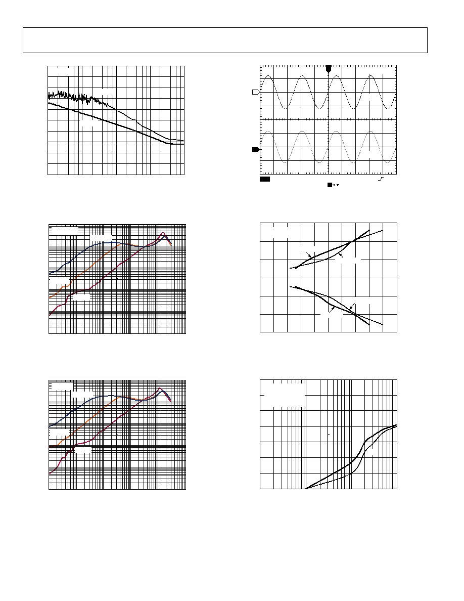
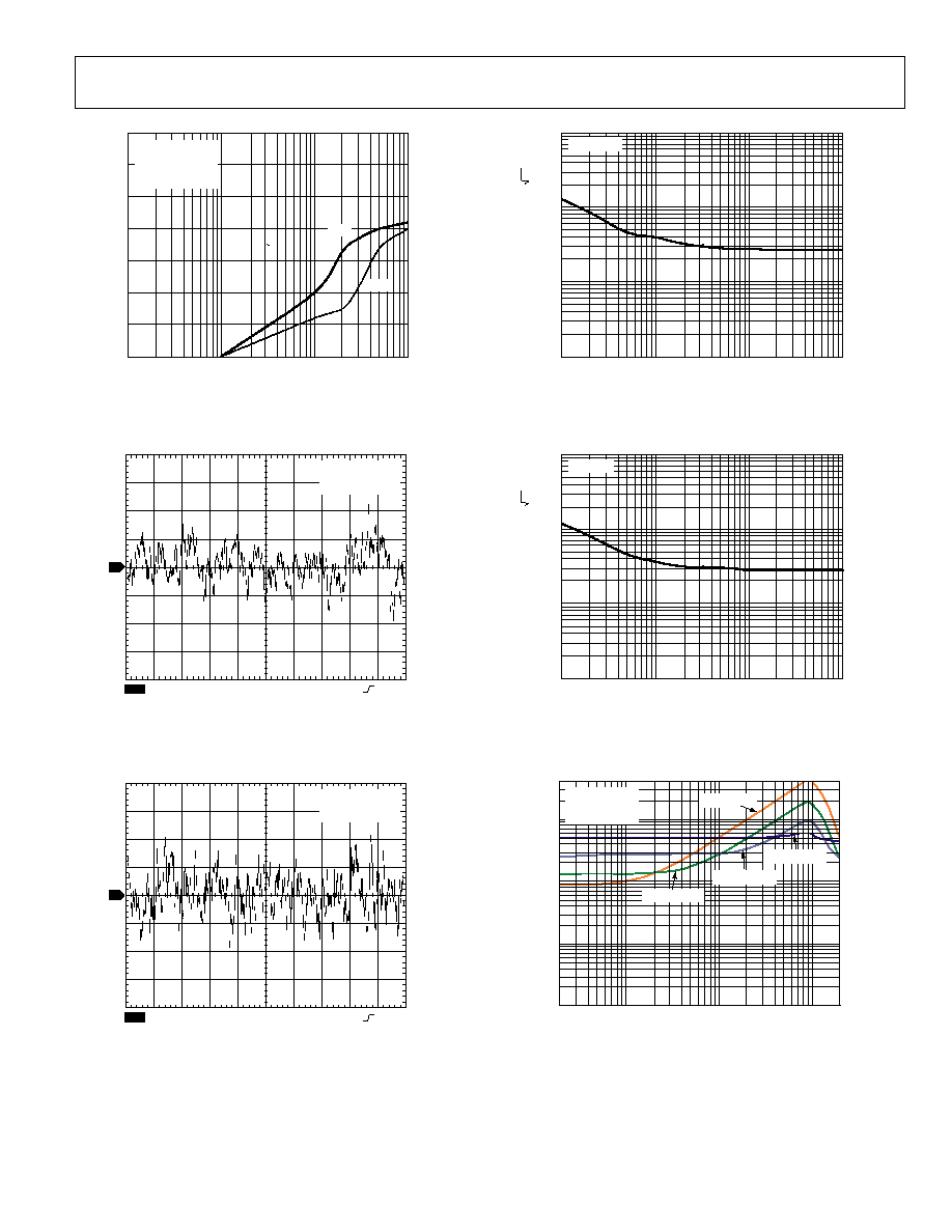
TYPICAL PERFORMANCE CHARACTERISTICS
0
10
20
30
40
50
60
70
FRE
Q
UE
NCY
≠0.60
≠0.55
≠0.50
≠0.45
≠0.40
≠0.35
≠0.30
≠0.25
≠0.20
≠0.15
≠0.10
≠0.05
0
0.05
0.10
0.15
0.20
0.25
0.30
0.35
0.40
0.45
0.50
0.55
0.60
V
OS
(mV)
05072-002
80
V
SY
=
±
13V
Figure 5. Input Offset Voltage
NUMBE
R OF AMP
L
IFIE
RS
OFFSET VOLTAGE (
µ
V/
∞
C)
05072-003
0
0.5
1.0
1.5
2.0
2.5
3.0
3.5
4.0
4.5
5.0
5.5
6.0
6.5
7.0
7.5
8.0
8.5
9.0
9.5
10.0
16
14
12
10
8
6
4
2
0
V
SY
=
±
13V
Figure 6. Offset Voltage Drift
0
10
20
30
40
50
60
70
FRE
Q
UE
NCY
≠0.60
≠0.55
≠0.50
≠0.45
≠0.40
≠0.35
≠0.30
≠0.25
≠0.20
≠0.15
≠0.10
≠0.05
0
0.05
0.10
0.15
0.20
0.25
0.30
0.35
0.40
0.45
0.50
0.55
0.60
V
OS
(mV)
05072-004
V
SY
=
±
2.5V
Figure 7. Input Offset Voltage
NUMBE
R OF AMP
L
IFIE
RS
T
C
V
OS
(
µ
V/
∞
C)
05072-005
0
0.5
1.0
1.5
2.0
2.5
3.0
3.5
4.0
4.5
5.0
5.5
6.0
6.5
7.0
7.5
8.0
8.5
9.0
9.5
10.0
0
2
4
6
8
10
12
14
16
18
20
V
SY
= 5V
V
CM
= 1.5V
Figure 8. Offset Voltage Drift
≠0.5
0
0.5
1.0
1.5
2.0
2.5
3.0
3.5
4.0
4.5
INP
U
T BIAS
(pA)
≠15 ≠13 ≠11 ≠9
≠7
≠5
≠3
≠1
1
3
5
7
9
11
13
15
V
CM
(V)
05072-006
V
SY
=
±
13V
T
A
= 25∞C
Figure 9. Input Bias Current vs. V
CM
≠0.4
≠0.3
≠0.2
≠0.1
0
0.1
INP
U
T BIAS
(pA)
0.2
0.3
0.4
≠15.0 ≠12.5 ≠10.0 ≠7.5
≠5.0
≠2.5
0
2.5
5.0
7.5
10.0 12.5 15.0
V
CM
(V)
05072-007
V
SY
=
±
13V
T
A
= 25∞C
0.5
≠0.5
Figure 10. Input Bias Current vs. V
CM
AD8641/AD8642
Rev. A | Page 7 of 16
INP
U
T BIAS
CURRE
NT (pA)
0.1
1
10
100
1000
50
75
0
25
100
125
150
TEMPERATURE (
∞
C)
05072-008
V
SY
=
±
13V
Figure 11. Input Bias Current vs. Temperature
≠1.0
≠0.8
≠0.6
≠0.4
≠0.2
0
0.2
0.4
0.6
0.8
1.0
INP
U
T BIAS
(pA)
≠5
≠4
≠3
≠2
≠1
0
1
2
3
4
5
V
CM
(V)
05072-009
V
SY
=
+5V OR
±
5V
Figure 12. Input Bias Current vs. V
CM
V
OS
(
µ
V)
≠15 ≠13 ≠11 ≠9
≠7
≠5
≠3
≠1
1
3
5
7
9
11
13
15
V
CM
(V)
05072-010
0
≠100
0
200
600
800
1000
400
100
500
700
900
300
V
SY
=
±
13V
Figure 13. Input Offset Voltage vs. V
CM
≠500
≠400
≠300
≠200
≠100
0
100
200
300
400
500
V
OS
(
µ
V)
1.0
1.5
0
0.5
2.0
2.5
V
CM
(V)
05072-011
V
SY
=
5V
Figure 14. Input Offset Voltage vs. V
CM
OPEN-
L
OOP GAIN (
V
/V)
10k
1M
100k
10M
LOAD RESISTANCE (k
)
0.1
10
1
100
05072-012
V
SY
=
±
13V
V
SY
=
±
2.5V
Figure 15. Open-Loop Gain vs. Load Resistance
A
VO
(
V
/mV)
1
100
10
1000
≠50
≠30
≠10
10
30
50
70
90
110
130
150
TEMPERATURE (
∞
C)
05072-013
A. V
SY
=
±
13V, V
O
=
±
11V, R
L
= 10k
B. V
SY
=
±
13V, V
O
=
±
11V, R
L
= 2k
C. V
SY
= +5V, V
O
= +0.5V/+4.5V, R
L
= 10k
D. V
SY
= +5V, V
O
= +0.5V/+4.5V, R
L
= 2k
E. V
SY
= +5V, V
O
= +0.5V/+4.5V, R
L
= 600
A
B
C
D
E
Figure 16. Open-Loop Gain vs. Temperature
AD8641/AD8642
Rev. A | Page 8 of 16
≠600
≠400
≠200
≠300
≠500
0
≠100
OFFSET VOLTAGE (
µ
V)
200
100
400
300
600
500
≠5
0
≠15
≠10
5
10
15
OUTPUT VOLTAGE (V)
05072-014
10k
1k
100k
V
SY
=
±
13V
Figure 17. Input Error Voltage vs. Output Voltage for Resistive Loads
≠350
≠250
≠150
≠200
≠300
≠50
≠100
INPUT VOLTAGE (
µ
V)
50
0
150
100
250
200
0
50
100
150
200
250
300
350
OUTPUT VOLTAGE FROM SUPPLY RAIL (mV)
05072-015
R
L
= 1k
POS RAIL
NEG RAIL
R
L
= 10k
R
L
= 2k
R
L
= 100k
R
L
= 100k
R
L
= 10k
R
L
= 1k
R
L
= 2k
V
SY
=
±
5V
Figure 18. Input Error Voltage vs. Output Voltage
Within 300 mV of Supply Rails
0
100
200
300
400
500
I
SY
(
µ
A)
600
700
800
4
8
12
16
20
24
28
V
SY
(V)
05072-016
+25∞C
≠55∞C
+125∞C
Figure 19. Quiescent Current vs. Supply Voltage at Different Temperatures
S
A
TURATION V
O
LTAGE
(mV
)
1
10
100
1000
10000
0.001
0.01
0.1
1
10
100
LOAD CURRENT (mA)
05072-017
≠
V
SY
≠ V
OL
V
SY
≠ V
OH
V
SY
=
±
13V
Figure 20. Output Saturation Voltage vs. Load Current
S
A
TURATION V
O
LTAGE
(mV
)
1
10
100
1000
10000
0.001
0.01
0.1
1
10
100
LOAD CURRENT (mA)
05072-018
V
OL
V
SY
≠ V
OH
V
SY
=
5V
Figure 21. Output Saturation Voltage vs. Load Current
≠30
≠135
≠90
≠45
0
45
90
135
180
225
270
315
≠20
≠10
0
10
20
30
40
50
60
70
10k
100k
1M
10M
PH
A
SE (
D
egrees)
GAIN
PHASE
V
SY
=
±
13V
R
L
= 2k
C
L
= 40pF
GAIN (
d
B)
FREQUENCY (Hz)
05072-019
Figure 22. Open-Loop Gain and Phase Margin vs. Frequency

AD8641/AD8642
Rev. A | Page 9 of 16
≠30
≠135
≠90
≠45
0
45
90
135
180
225
270
315
≠20
≠10
0
10
20
30
40
50
60
70
10k
100k
1M
10M
PH
A
SE (
D
egrees)
GAIN
PHASE
GAIN (
d
B)
FREQUENCY (Hz)
05072-020
V
SY
= 5V
R
L
= 2k
C
L
= 40pF
Figure 23. Open-Loop Gain and Phase Margin vs. Frequency
FREQUENCY (Hz)
≠30
≠20
≠10
0
10
20
30
40
50
60
70
1k
10k
100k
1M
10M
GAIN (
d
B)
V
SY
=
±
13V
R
L
= 2k
C
L
= 40pF
G = +100
G = +1
G = +10
05072-021
Figure 24. Closed-Loop Gain vs. Frequency
FREQUENCY (Hz)
≠30
≠20
≠10
0
10
20
30
40
50
60
70
1k
10k
100k
1M
10M
GAIN (
d
B)
G = +100
G = +1
G = +10
05072-022
V
SY
= 5V
R
L
= 2k
C
L
= 40pF
Figure 25. Closed-Loop Gain vs. Frequency
≠60
≠40
≠20
0
20
40
60
80
100
120
140
1k
10k
100k
1M
10M
FREQUENCY (Hz)
CMRR (dB)
05072-023
V
SY
=
±
13V
Figure 26. CMRR vs. Frequency
≠60
≠40
≠20
0
20
40
60
80
100
120
140
1k
10k
100k
1M
10M
FREQUENCY (Hz)
CMRR (dB)
05072-024
V
SY
= 5V
Figure 27. CMRR vs. Frequency
≠60
≠40
≠20
0
20
40
60
80
100
120
140
1k
10k
100k
1M
10M
FREQUENCY (Hz)
PSR
R
(
d
B
)
05072-025
+PSRR
≠PSRR
V
SY
=
±
13V
Figure 28. PSRR vs. Frequency
AD8641/AD8642
Rev. A | Page 10 of 16
≠60
≠40
≠20
0
20
40
60
80
100
120
140
1k
10k
100k
1M
10M
FREQUENCY (Hz)
P
S
RR (dB)
05072-026
V
SY
= 5V
+PSRR
≠PSRR
Figure 29. PSRR vs. Frequency
0.01
0.1
1
10
100
1000
Z
OUT
(
)
1k
10k
100k
1M
10M
100M
FREQUENCY (Hz)
05072-027
G = +100
G = +10
G = +1
V
SY
=
±
13V
Figure 30. Output Impedance vs. Frequency
0.01
0.1
1
10
100
1000
Z
OUT
(
)
1k
10k
100k
1M
10M
100M
FREQUENCY (Hz)
05072-028
G = +100
G = +10
G = +1
V
SY
=
5V
Figure 31. Output Impedance vs. Frequency
≠1.0
≠0.8
≠0.6
≠0.4
≠0.2
0
0.2
0.4
0.6
0.8
1.0
INP
U
T BIAS
(pA)
≠5
≠4
≠3
≠2
≠1
0
1
2
3
4
5
V
CM
(V)
05072-009
05072-029
CH1
10.0V
CH2 10.0V
M400
µ
s
A CH1 1.00V
1
T
0.00000s
2
V
IN
V
OUT
T
V
SY
=
±
13V
Figure 32. No Phase Reversal
≠15
≠10
≠5
0
5
10
15
OUTPUT SW
ING (V)
0
0.2
0.4
0.6
0.8
1.0
1.2
1.4
1.6
1.8
2.0
SETTLING TIME (
µ
s)
05072-030
V
S
=
±
13V
GAIN = +5
TS ≠ (0.1%)
TS ≠ (1%)
TS + (0.1%)
TS + (1%)
Figure 33. Output Swing and Error vs. Settling Time
0
10
20
30
40
50
60
70
OVER
SH
OOT (
%
)
CAPACITANCE (pF)
1
100
10
1000
05072-031
OS+
OS≠
V
S
=
±
13V
R
L
= 10k
V
IN
= 100mV p-p
A
V
= +1
Figure 34. Small Signal Overshoot vs. Load Capacitance
AD8641/AD8642
Rev. A | Page 11 of 16
0
10
20
30
40
50
60
70
OVER
SH
OOT (
%
)
CAPACITANCE (pF)
1
100
10
1000
05072-032
OS+
OS≠
V
S
=
±
2.5V
R
L
= 10k
V
IN
= 100mV p-p
A
V
= +1
Figure 35. Small Signal Overshoot vs. Load Capacitance
≠1.0
≠0.8
≠0.6
≠0.4
≠0.2
0
0.2
0.4
0.6
0.8
1.0
INP
U
T BIAS
(pA)
≠5
≠4
≠3
≠2
≠1
0
1
2
3
4
5
V
CM
(V)
05072-009
05072-033
CH1
1.00V
M1.00s
A CH1
≠20.0V
1
V
S
=
±
13V
G = +1M
CH1 p-p = 4.26V
Figure 36. 0.1 Hz to 10 Hz Noise
≠1.0
≠0.8
≠0.6
≠0.4
≠0.2
0
0.2
0.4
0.6
0.8
1.0
I
N
P
U
T BI
AS
(pA)
≠5
≠4
≠3
≠2
≠1
0
1
2
3
4
5
V
CM
(V)
0
5072-009
05072-034
CH1
1.00V
M1.00s
A CH1
≠20.0V
1
V
S
=
±
2.5V
G = +1M
CH1 p-p = 4.06V
Figure 37. 0.1 Hz to 10 Hz Noise
VOLTA
GE N
O
ISE D
E
N
S
ITY (
n
V/ H
z
)
1
10
100
1k
FREQUENCY (Hz)
10
1k
100
10k
05072-035
V
SY
=
±
13V
Figure 38. Voltage Noise Density
VOLTA
GE N
O
ISE D
E
N
S
ITY (
n
V/ H
z
)
1
10
100
1k
FREQUENCY (Hz)
10
1k
100
10k
05072-036
V
SY
=
5V
Figure 39. Voltage Noise Density
0.000001
0.00001
0.0001
0.001
1k
100
1
20k
THD + NOIS
E
(%)
FREQUENCY (Hz)
05072-037
0.004
1V p-p INPUT
2V p-p INPUT
4V p-p INPUT
8V p-p INPUT
V
SY
=
±
13V
LOAD = 100k
GAIN = +1
10k
Figure 40. Total Harmonic Distortion + Noise vs. Frequency

AD8641/AD8642
Rev. A | Page 12 of 16
≠160
≠150
≠140
≠130
≠120
≠110
≠100
≠90
≠80
≠70
≠60
≠50
≠40
(dB)
20
100
1k
10k
100k
FREQUENCY (Hz)
05072-041
≠
+
V
IN
2k
≠
+
2k
2k
20k
V
IN
= 18V p-p
V
IN
= 4.5V p-p
V
IN
= 9V p-p
Figure 41. Channel Separation

AD8641/AD8642
Rev. A | Page 13 of 16
OUTLINE DIMENSIONS
COMPLIANT TO JEDEC STANDARDS MO-203AA
0.30
0.15
0.10 MAX
1.00
0.90
0.70
SEATING
PLANE
0.22
0.08
1.10
0.80
0.30
0.10
4
5
1
2
3
PIN 1
0.65 BSC
2.20
2.00
1.80
2.40
2.10
1.80
1.35
1.25
1.15
0.10 COPLANARITY
0.40
0.10
Figure 42. 5-Lead Thin Shrink Small Outline Transistor Package [SC70]
(KS-5)
Dimensions shown in millimeters
0.25 (0.0098)
0.17 (0.0067)
1.27 (0.0500)
0.40 (0.0157)
0.50 (0.0196)
0.25 (0.0099)
◊
45∞
8∞
0∞
1.75 (0.0688)
1.35 (0.0532)
SEATING
PLANE
0.25 (0.0098)
0.10 (0.0040)
4
1
8
5
5.00 (0.1968)
4.80 (0.1890)
4.00 (0.1574)
3.80 (0.1497)
1.27 (0.0500)
BSC
6.20 (0.2440)
5.80 (0.2284)
0.51 (0.0201)
0.31 (0.0122)
COPLANARITY
0.10
CONTROLLING DIMENSIONS ARE IN MILLIMETERS; INCH DIMENSIONS
(IN PARENTHESES) ARE ROUNDED-OFF MILLIMETER EQUIVALENTS FOR
REFERENCE ONLY AND ARE NOT APPROPRIATE FOR USE IN DESIGN
COMPLIANT TO JEDEC STANDARDS MS-012-AA
Figure 43. 8-Lead Standard Small Outline Package [SOIC_N]
(R-8)
Dimensions shown in millimeters and (inches)
0.80
0.60
0.40
8∞
0∞
4
8
1
5
4.90
BSC
PIN 1
0.65 BSC
3.00
BSC
SEATING
PLANE
0.15
0.00
0.38
0.22
1.10 MAX
3.00
BSC
COPLANARITY
0.10
0.23
0.08
COMPLIANT TO JEDEC STANDARDS MO-187-AA
Figure 44. 8-Lead Mini Small Outline Package [MSOP]
(RM-8)
Dimensions shown in millimeters

AD8641/AD8642
Rev. A | Page 14 of 16
ORDERING GUIDE
Model
Temperature Range
Package Description Package
Option
Branding
AD8641AKSZ-R2
1
≠40∞C to +125∞C
5-Lead SC70
KS-5
A07
AD8641AKSZ-REEL7
1
≠40∞C to +125∞C
5-Lead SC70
KS-5
A07
AD8641AKSZ-REEL
1
≠40∞C to +125∞C
5-Lead SC70
KS-5
A07
AD8641ARZ
1
≠40∞C to +125∞C
8-lead SOIC_N
R-8
AD8641ARZ-REEL7
1
≠40∞C to +125∞C
8-lead SOIC_N
R-8
AD8641ARZ-REEL
1
≠40∞C to +125∞C
8-lead SOIC_N
R-8
AD8642ARMZ-R2
1
≠40∞C to +125∞C
8-lead MSOP
RM-8
A0A
AD8642ARMZ-REEL
1
≠40∞C to +125∞C
8-lead MSOP
RM-8
A0A
AD8642ARZ
1
≠40∞C to +125∞C
8-lead SOIC
R-8
AD8642ARZ-REEL7
1
≠40∞C to +125∞C
8-lead SOIC
R-8
AD8642ARZ-REEL
1
≠40∞C to +125∞C
8-lead SOIC
R-8
1
Z = Pb-free part.

AD8641/AD8642
Rev. A | Page 15 of 16
NOTES

AD8641/AD8642
Rev. A | Page 16 of 16
NOTES
© 2005 Analog Devices, Inc. All rights reserved. Trademarks and
registered trademarks are the property of their respective owners.
D05072≠0≠3/05(A)