 | ÐлекÑÑоннÑй компоненÑ: AD8664 | СкаÑаÑÑ:  PDF PDF  ZIP ZIP |
Äîêóìåíòàöèÿ è îïèñàíèÿ www.docs.chipfind.ru
REV. PrA 10/5/2004
One Technology Way, P.O. Box 9106, Norwood, MA 02062-9106, U.S.A.
Tel: 781/329-4700
www.analog.com
Information furnished by Analog Devices is believed to be accurate and
reliable. However, no responsibility is assumed by Analog Devices for its use,
nor for any infringements of patents or other rights of third parties that may
result from its use. No license is granted by implication or otherwise under any
patent or patent rights of Analog Devices. Trademarks and registered
trademarks are the property of their respective companies.
Fax: 781/326-8703
© 2004 Analog Devices, Inc. All rights reserved.
16V Low Cost, High Performance
CMOS Rail-to-Rail
Operational Amplifiers
Preliminary Technical Data
AD8661/AD8662/AD8664
FEATURES
Low Offset Voltage: 75
µ
V max
Low Input Bias Currents 1pA Max
Single-Supply Operation: 5 to 16 Volts
Dual-Supply Operation: +/- 2.5 to +/-8 Volts
Low Noise: 10 nV/
Hz
Wide Bandwidth: 4 MHz
Unity Gain Stable
APPLICATIONS
Multi-pole Filters
Sensors
Medical Equipment
Consumer Audio
Photodiode amplification
ADC driver
GENERAL DESCRIPTION
The AD8661, AD8662 and AD8664 are single, dual and quad
rail-to-rail output single supply amplifiers that use Analog
Devices' patented DigiTrim® trimming technique to achieve
low offset voltage. The AD8661 family features an extended
operating range with supply voltages up to 16 V. They also
feature low input bias currents, wide signal bandwidth, and low
input voltage and current noise.
The combination of low offsets, very low input bias currents,
and wide supply range make these amplifiers useful in a wide
variety of applications normally associated with much higher
priced JFET amplifiers. Systems utilizing high impedance
sensors, such as photo-diodes benefit from the combination of
low input bias current, low noise, low offset and bandwidth.
The wide operating voltage range matches today's high
performance ADCs and DACs. Audio applications and
medical monitoring equipment can take advantage of the high
input impedance, low voltage and current noise, wide
bandwidth and the lack of "popcorn" noise (found in many
other low input bias current amplifiers).
The AD8661, AD8662 and AD8664 are specified over the
extended industrial (-40° to +125°C) temperature range. The
AD8661, single, is available in the tiny 8-lead LFCSP (MO-
220) 3mm x 3mm and 8-lead SOIC package. The AD8662,
dual, is available in the 8-lead micro-SOIC and narrow SOIC
surface mount packages. The AD8664, quad, is available in
14-lead TSSOP and narrow 14-pin SOIC packages.
LFCSP, MSOP and TSSOP versions are available in tape and
reel only.
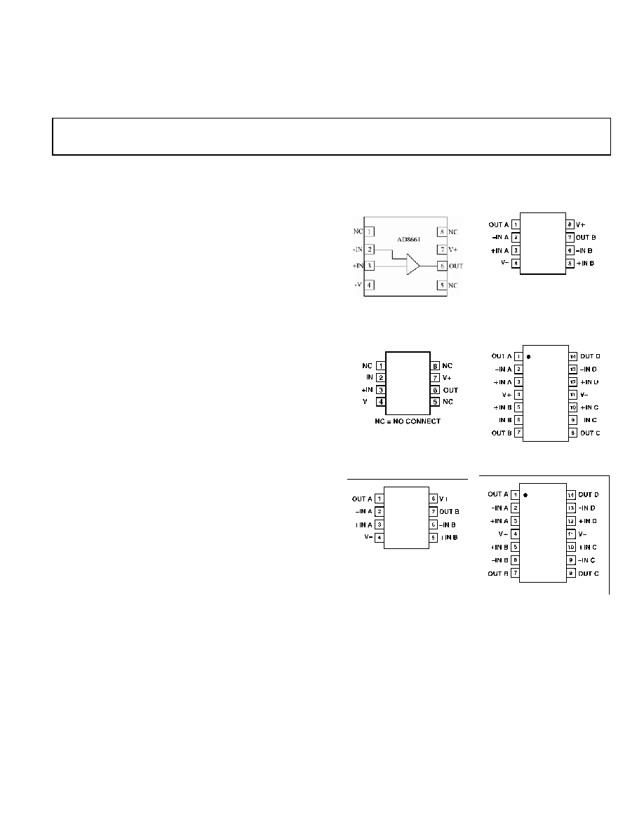
PIN CONFIGURATIONS
8-Lead LFCSP
(CP-8)
3mm x 3mm
8-Lead MSOP
(RM-8)
8-Lead SO
(R-8)
14-Lead TSSOP
(RU-14)
8-Lead SO
(R-8)
14-Lead SO
(R-14)
AD8662
AD8662
AD8664
AD8664
AD8661
a

Preliminary Technical Data
AD8661/AD8662/AD8664
-
2-
Rev PrA 10/5/04
ELECTRICAL CHARACTERISTICS
(V
S
=+5.0V, V
CM
= V
S
/2, T
A
=+25°C unless otherwise
noted)
Parameter
Symbol
Conditions
Min
Typ
Max
Units
INPUT CHARACTERISTICS
Offset Voltage
V
OS
V
SY
= 8V, V
CM
= 3V
75
µ
V
V
CM
= 0.1V to 3.0V
30
300
µ
V
-40°<
T
A
< +85°C
650
µ
V
-40°<
T
A
< +125°C
750
µ
V
Input Bias Current
I
B
0.3
1 pA
-40°<
T
A
< +85°C
50
pA
-40°<
T
A
< +125°C
300
pA
Input Offset Current
I
OS
0.2
TBD
pA
-40°<
T
A
< +85°C
20
pA
-40°<
T
A
< +125°C
75
pA
Input Voltage Range
tbd
3.0
V
Common-Mode Rejection Ratio
CMRR
V
CM
= 0.1V to 3.0V
80
95
dB
Large Signal Voltage Gain
A
VO
R
L
= 10 k
V
O
= 0.5V to 4.5V
70
100
V/mV
Offset Voltage Drift
V
OS
/
T
3
10
µ
V/°C
OUTPUT CHARACTERISTICS
Output Voltage High
V
OH
I
L
= 1mA
4.80
4.85
V
I
L
= 10mA
4.80
4.85
V
-40°C < T
A
< +125°C
4.75
V
Output Voltage Low
V
OL
I
L
= 1mA
60
120
mV
V
OL
I
L
= 1mA
60
120
mV
-40°C < T
A
< +125°C
150
mV
Output Current
I
OUT
±
19
mA
Closed Loop Output Impedance
Z
OUT
f=1 MHz, A
V
= 1
65
POWER SUPPLY
Power Supply Rejection Ratio
PSRR
V
S
= 5 V to 16 V
80
95
dB
Supply Current/Amplifier
I
SY
V
O
= 0V
1.2
1.8
mA
-40°<
T
A
< +125°C
2.0
mA
DYNAMIC PERFORMANCE
Slew Rate
SR
R
L
=10 k
3
V/
µ
s
Settling Time
t
s
To 0.1%, 0 V to 1V step
<1
µ
s
Gain Bandwidth Product
GBP
4
MHz
Phase Margin
Øo
C
L
= 15 pF
60
degrees
NOISE PERFORMANCE
Peak-to-Peak Noise
e
n
p-p
f=0.1Hz to 10 Hz
2.5
µ
V p-p
Voltage Noise Density
e
n
f=1kHz
12
nV/
Hz
Voltage Noise Density
e
n
f=10kHz
10
nV/
Hz
Current Noise Density
i
n
f=1kHz
0.1
pA/
Hz

Preliminary Technical Data
AD8661/AD8662/AD8664
-
3-
Rev PrA 10/5/04
ELECTRICAL CHARACTERISTICS
(V
S
=
±
8.0V, V
CM
= 0, T
A
=+25°C unless otherwise noted)
Parameter
Symbol
Conditions
Min
Typ
Max
Units
INPUT CHARACTERISTICS
Offset Voltage
V
OS
V
SY
= 8V, V
CM
= 3V
75
µ
V
V
CM
= -8.1V to +6.0V
30
300
µ
V
-40°<
T
A
< +85°C
650
µ
V
-40°<
T
A
< +125°C
750
µ
V
Input Bias Current
I
B
0.3
1 pA
-40°<
T
A
< +85°C
50
pA
-40°<
T
A
< +125°C
300
pA
Input Offset Current
I
OS
0.2
TBD
pA
-40°<
T
A
< +85°C
20
pA
-40°<
T
A
< +125°C
75
pA
Input Voltage Range
tbd
6
V
Common-Mode Rejection Ratio
CMRR
V
CM
= -8.1V to +6.0V
80
95
dB
Large Signal Voltage Gain
A
VO
R
L
=10 k
V
O
= -7.5V to+7.5V
70
85
V/mV
Offset Voltage Drift
V
OS
/
T
3
10
µ
V/°C
OUTPUT CHARACTERISTICS
Output Voltage High
V
OH
I
L
= 1mA
7.90
7.95
V
I
L
= 10mA
7.6
7.7
V
-40°C < T
A
< +125°C
7.4
V
Output Voltage Low
V
OL
I
L
= 1mA
-7.97
-7.93
mV
I
L
= 10mA
-7.8
-7.7
mV
-40°C < T
A
< +125°C
-7.5
mV
Output Current
I
OUT
±
140
mA
Closed Loop Output Impedance
Z
OUT
f=1 MHz, A
V
= 1
45
POWER SUPPLY
Power Supply Rejection Ratio
PSRR
V
S
= 5V to 16V
80
95
dB
Supply Current/Amplifier
I
SY
V
O
= 0V
1.5
1.8
mA
-40°<
T
A
< +125°C
2.0
mA
DYNAMIC PERFORMANCE
Slew Rate
SR
R
L
=10 k
3
V/
µ
s
Settling Time
t
s
To 0.1%, 0 V to 1V step
<1
µ
s
Gain Bandwidth Product
GBP
4
MHz
Phase Margin
Øo
C
L
= 15 pF
60 degrees
NOISE PERFORMANCE
Peak-to-Peak Noise
e
n
p-p
f=0.1Hz to 10 Hz
2.5
µ
V p-p
Voltage Noise Density
e
n
f=1kHz
12
nV/
Hz
Voltage Noise Density
e
n
f=10kHz
10
nV/
Hz
Current Noise Density
i
n
f=1kHz
0.1
pA/
Hz
Preliminary Technical Data
AD8661/AD8662/AD8664
-
4-
Rev PrA 10/5/04
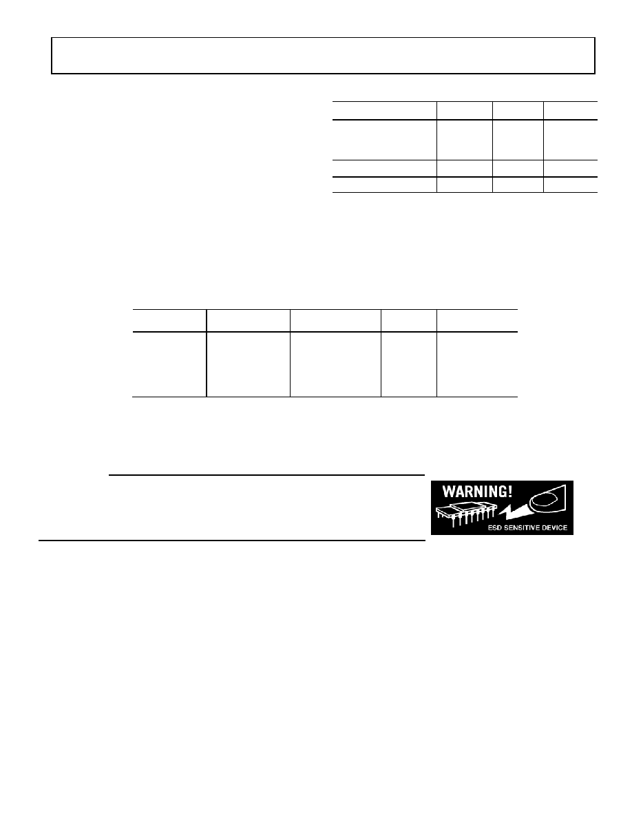
ABSOLUTE MAXIMUM RATINGS
1
Supply voltage.........................................................................+18V
Input Voltage ....................................................................Gnd to Vs
Differential Input Voltage .......................................................±18V
Output Short-Circuit Duration to Gnd
2
.....Observe Derating Curves
Storage Temperature Range
R, CP, RM, RU Package................................-65°C to +150°C
Operating Temperature Range
AD8661/AD8662/AD8664 ............................-40°C to +125°C
Junction Temperature Range
R, CP, RM, RU Package................................-65°C to +150°C
Lead Temperature Range (Soldering, 60 Sec)
............. +300°C
Package Type
JA
JC Units
8-Pin LFCSP (CP)
--
°C/W
8-Pin microSOIC (RM)
210
45
°C/W
8-Pin SOIC (R)
158
43
°C/W
14-Pin SOIC (R)
120
36
°C/W
14-Pin TSSOP (RU)
180
35
°C/W
NOTES
1 Absolute maximum ratings apply at 25°C, unless otherwise noted.
2 JA is specified for the worst-case conditions, i.e., JAis specified for device soldered
in circuit board for surface mount packages.
ORDERING GUIDE
Model
Temperature
Range
Package
Description
Package
Option
Branding
Information
AD8661ACP
-40°C to +125°C
8-Pin LFCSP
CP-8
AD8661ARZ
-40°C to +125°C
8-Pin SOIC
R-8
AD8662ARMZ -40°C to +125°C
8-Pin micro-SOIC
RM-8
AD8662ARZ
-40°C to +125°C
8-Pin SOIC
R-8
AD8664ARZ
-40°C to +125°C
14-Pin SOIC
R-14
AD8664ARUZ -40°C to +125°C
14-Pin TSSOP
RU-14
CAUTION
ESD (electrostatic discharge) sensitive device. Electrostatic charges as high as 1500 V
readily accumulate on the human body and test equipment and can discharge without
detection. Although this device features proprietary ESD protection circuitry, permanent
damage may occur on devices subjected to high-energy electrostatic discharges.
Therefore, proper ESD precautions are recommended to avoid performance degradation or
loss of functionality.
Preliminary Technical Data
AD8661/AD8662/AD8664
-
5-
Rev PrA 10/5/04
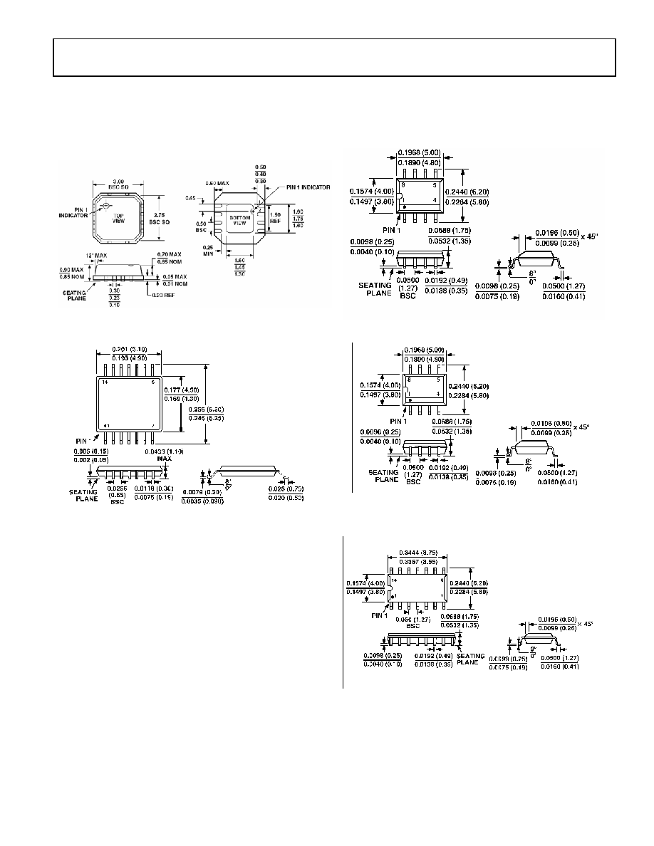
OUTLINE DIMENSIONS
8-Lead LFCSP
(CP-8 Suffix)
8-Lead SOIC
(RM-8)
14-Lead TSSOP
(RU-14)
8-Lead SO
(R-8)
14-Lead SO
(R-14)
PR05200-0-10/04(PRA)