 | –≠–ª–µ–∫—Ç—Ä–æ–Ω–Ω—ã–π –∫–æ–º–ø–æ–Ω–µ–Ω—Ç: AD8675 | –°–∫–∞—á–∞—Ç—å:  PDF PDF  ZIP ZIP |
Information furnished by Analog Devices is believed to be accurate and
reliable. However, no responsibility is assumed by Analog Devices for its use,
nor for any infringements of patents or other rights of third parties which may
result from its use. No license is granted by implication or otherwise under any
patent or patent rights of Analog Devices.
One Technology Way, P.O. Box 9106, Norwood, MA 02062-9106, U.S.A.
Tel: 617/329-4700
World Wide Web Site: http://www.analog.com
Fax: 617/326-8703
© Analog Devices, Inc., 2005
AD8675 -
1 -
Rev. PrA 5/11/2005
36V Precision, 2.5 nV/Hz,
Rail-to-Rail Output Amplifier
Preliminary Technical Data
AD8675
FEATURES
Very Low Voltage Noise 2.5nV/
Hz
Rail-to-Rail Output Swing
Low Input Bias Current: 5 nA Max
Very Low Offset Voltage: 50 µV Max
Low Input Offset Drift: 0.6 µV/
∞C Max
Very High Gain: 120 dB
Wide Bandwidth: 10MHz
± 5
V to
±
15V Operation
APPLICATIONS
Precision Instrumentation
PLL Filters
Laser Diode Control Loops
Strain Gage Amplifiers
Medical Instrumentation
Thermocouple Amplifiers
GENERAL DESCRIPTION
This new precision amplifier has ultra-low offset, drift and
voltage noise combined with very low input bias currents over
the full operating temperature range. The AD8675 is a
precision, wide bandwidth amplifier featuring rail-to-rail output
swings and very low noise. Operation is fully specified from
±5V to ±15 volts.
The AD8675 combines the R-R output of the OP184 with wide
bandwidth and even lower voltage noise and with the precision
and low power consumption of the industry-standard OP07
amplifier. Unlike other low noise R-R amplifiers the AD8675
has very low input bias current and low input current noise.
With an offset voltage of only 20µV, offset drift of 0.2 µV/∞C
and noise of only 0.25uV P-P (0.1Hz to 10 Hz) the AD8675 is
perfectly suited for applications where large error sources
cannot be tolerated. For applications with even lower offset
tolerances, the proprietary nulling capability allows a
combination of both device and system offset errors up to
1mV(referred to the input) to be compensated externally. Unlike
previous circuits, the AD8675 accommodates this adjustment
without adversely affecting the offset drift, CMRR and PSRR of
the amplifier. Precision Instrumentation, PLL and other
precision filter circuits, position and pressure sensors, medical
instrumentation, and strain gage amplifiers benefit greatly from
the very low noise, low input bias current and wide bandwidth.
Many systems may take advantage of the low noise, DC
precision and rail-to-rail output swing provided by the AD8675
to maximize SNR and dynamic range.
The smaller packages and low power consumption afforded by
the AD8675 allow maximum channel density or minimum
board size for space-critical equipment.
The AD8675 is specified for the extended industrial (-40∞ to
+125∞C) temperature range. The AD8675 amplifier is
available in the tiny MSOP-8 and the popular 8-pin narrow
SOIC lead-free packages. MSOP packaged devices are only
available in Tape-and-Reel format.
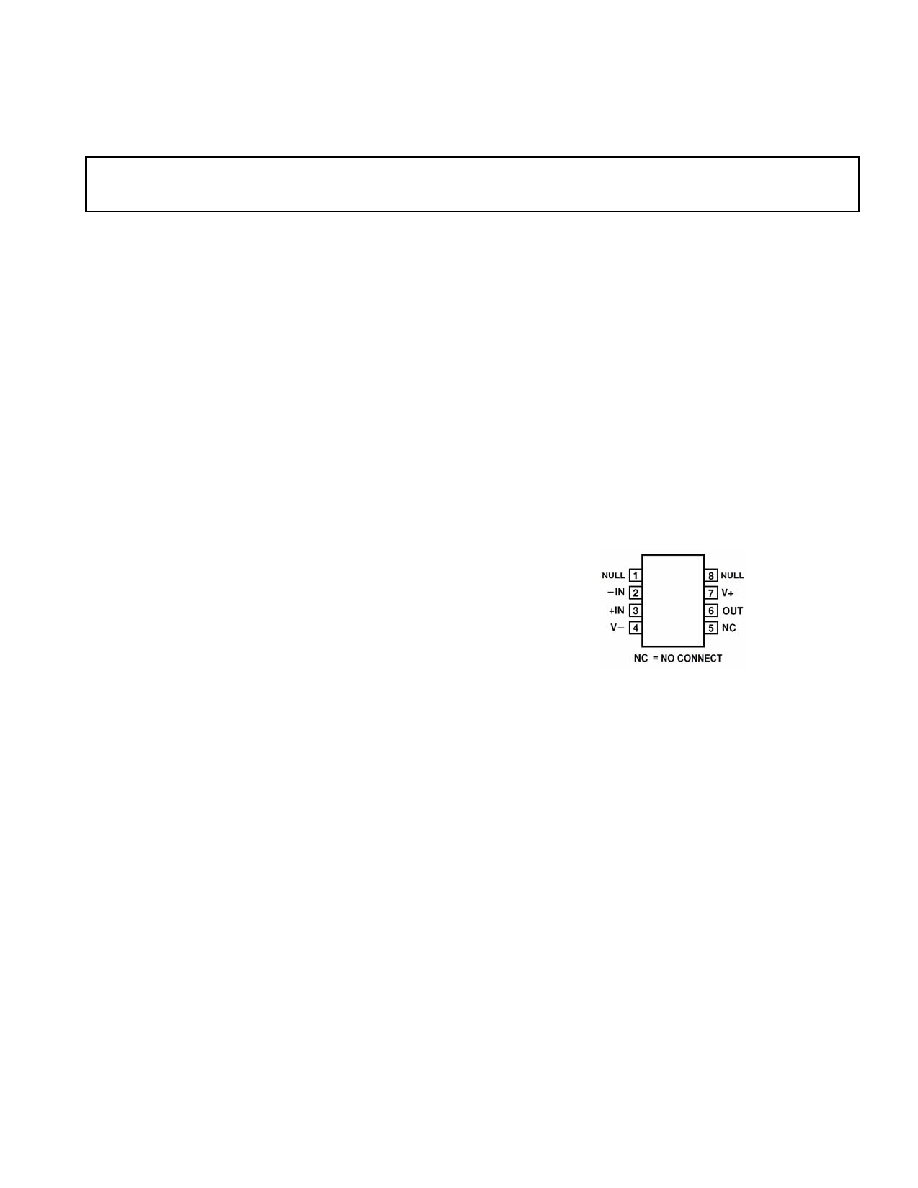
8-Lead SOIC/8-Lead MSOP
(R-8/RM-8)
AD8675
a

Preliminary Technical Data
AD8675
AD8675 ≠ 2 ≠ Rev. PrA 5/11/2005
ELECTRICAL SPECIFICATIONS
(VS=±5.0V, VCM = 0V, VO=0V, TA=+25∞C unless otherwise specified.)
Parameter
Symbol
Conditions
Min
Typ
Max
Units
INPUT CHARACTERISTICS
Offset Voltage
V
OS
20 50
µV
Input Bias Current
I
B
2 5
nA
-40∞C
T
A
+125∞C
3
6
nA
Input Offset Current
I
OS
0.5 1
nA
-40∞C
T
A
+125∞C
2
nA
Input Voltage Range
-3.5
3.5
V
Common-Mode Rejection Ratio
CMRR
V
CM
= -3.5V to 3.5V
110
120
dB
-40∞C
T
A
+125∞C
105
115
dB
Open Loop Gain (Note 1)
A
VO
R
L
= 2 k
to Ground,
120
dB
Vo=-4.0V to 4.0V
-40∞C
T
A
+125∞C
120
dB
Offset Voltage Drift
V
OS
/
T -40∞C
T
A
+125∞C
0.2
0.6
µV/∞C
OUTPUT CHARACTERISTICS
Output Voltage High
V
OH
R
L
= 2k
to Ground
4.9
4.92
V
-40∞C
T
A
+125∞C
4.8
4.85
V
R
L
= 600
to Ground
4.5
4.55
V
-40∞C
T
A
+125∞C
4.4
4.45
V
Output Voltage Low
V
OL
R
L
= 2k
to Ground
-4.92
-4.9
V
-40∞C
T
A
+125∞C
-4.85
-4.8
V
R
L
= 600
to Ground
-4.55
-4.5
V
-40∞C
T
A
+125∞C
-4.45
4.4
V
Short Circuit Limit
I
SC
40
mA
-40∞C
T
A
+125∞C
30
mA
Output Current
I
O
±
20
mA
-40∞C
T
A
+125∞C
± 15
mA
POWER SUPPLY
Power Supply Rejection Ratio
PSRR
V
S
=
=
±5.0V
to
±15.0V
100
110
dB
-40∞C
T
A
+125∞C
100
110
dB
Supply Current/Amplifier
I
SY
V
O
= 0V
2.5
3
mA
-40∞C
T
A
+125∞C
3.2
mA
DYNAMIC PERFORMANCE
Slew Rate
SR
R
L
=2 k
1
V/µs
Gain Bandwidth Product
GBP
10
MHz
NOISE PERFORMANCE
Voltage Noise
e
n p-p
0.1 to 10 Hz
0.1
µV
p-p
Voltage Noise Density
e
n
f = 1 kHz
2.5
nV/
Hz
Current Noise Density
in
f =10 Hz
0.3
pA/
Hz

Preliminary Technical Data
AD8675
AD8675 ≠ 3 ≠ Rev. PrA 5/11/2005
ELECTRICAL SPECIFICATIONS
(VS = ±15V, VCM = 0V, VO = 0V, TA=+25∞C unless otherwise specified.)
Parameter
Symbol
Conditions
Min
Typ
Max
Units
INPUT CHARACTERISTICS
Offset Voltage
V
OS
20 50
µV
Input Bias Current
I
B
2.5 5
nA
-40∞C
T
A
+125∞C
3
6
nA
Input Offset Current
I
OS
50 1
nA
-40∞C
T
A
+125∞C
2
nA
Input Voltage Range
-13.5
13.5
V
Common-Mode Rejection Ratio
CMRR
V
CM
= -12.5V to 12.5V
110
120
dB
-40∞C
T
A
+125∞C
105
110
dB
Open Loop Gain
A
VO
R
L
= 2k
to Ground,
120
dB
Vo=-14.0V to 14.0V
-40∞C
T
A
+125∞C
120
dB
Offset Voltage Drift
V
OS
/
T -40∞C
T
A
+125∞C
0.2
0.6
µV/∞C
OUTPUT CHARACTERISTICS
Output Voltage High
V
OH
R
L
= 2k
to Ground
14.9
14.95
V
-40∞C
T
A
+125∞C
14.8
14.85
V
R
L
= 600
to Ground
14.5
14.55
V
-40∞C
T
A
+125∞C
14.4
14.45
V
Output Voltage Low
V
OL
R
L
= 2k
to Ground
-14.95
-14.9
V
-40∞C
T
A
+125∞C
-14.85
-14.8
V
R
L
= 600
to Ground
-14.55
-14.5
V
-40∞C
T
A
+125∞C
-14.45
-14.4
V
Short Circuit Limit
I
SC
40
mA
-40∞C
T
A
+125∞C
30
mA
Output Current
I
O
±
20
mA
-40∞C
T
A
+125∞C
± 15
mA
POWER SUPPLY
Power Supply Rejection Ratio
PSRR
V
S
=
=
±5.0V
to
±15.0V
100
110
dB
-40∞C
T
A
+125∞C
100
110
dB
Supply Current/Amplifier
I
SY
V
O
= 0V
2.5
3
mA
-40∞C
T
A
+125∞C
3.2
mA
DYNAMIC PERFORMANCE
Slew Rate
SR
R
L
=10 k
1
V/µs
Gain Bandwidth Product
GBP
10
MHz
NOISE PERFORMANCE
Voltage Noise
e
n p-p
0.1 to 10 Hz
0.1
µV
p-p
Voltage Noise Density
e
n
f = 1 kHz
2.5
nV/
Hz
Current Noise Density
in
f = 10 Hz
0.3
pA/
Hz

Preliminary Technical Data
AD8675
AD8675 ≠ 4 ≠ Rev. PrA 5/11/2005
ABSOLUTE MAXIMUM RATINGS
Supply Voltage .......................................................................
±18V
Input Voltage....................................................................
±
Vsupply
Differential Input Voltage .....................................................
±0.7V
Output Short-Circuit Duration to Gnd .............................. Indefinite
Storage Temperature Range
RM, R Package.............................................. -65∞C to +150∞C
Operating Temperature Range
AD8675 ......................................................... -40∞C to +125∞C
Junction Temperature Range
RM, R Package.............................................. -65∞C to +150∞C
Lead Temperature Range (Soldering, 10 sec) ......................+300∞C
Package Type
JA
1
JC Units
8-Pin MSOP (RM)
210
45
∞C/W
8-Pin SOIC (R)
158
43
∞C/W
NOTES
1 JA is specified for the worst case conditions, i.e., JA is specified for device in socket
for P-DIP packages;
JAis specified for device soldered in circuit board for SOIC and
TSSOP packages.
ORDERING GUIDE
Temperature
Package Package
Model Range Description
Option
AD8675ARMZ -40∞C to +125∞C 8-Pin MSOP
RM-8
AD8675ARZ
-40∞C to +125∞C 8-Pin SOIC
R-8
Stresses above those listed under Absolute Maximum Ratings
may cause permanent damage to the device. This is a stress
rating only; functional operation of the device at these or any
other conditions above those listed in the operational sections
of this specification is not implied. Exposure to absolute
maximum rating conditions for extended periods may affect
device reliability.
PR05564-0-5/05(PrA)