 | ÐлекÑÑоннÑй компоненÑ: AD8692 | СкаÑаÑÑ:  PDF PDF  ZIP ZIP |
Äîêóìåíòàöèÿ è îïèñàíèÿ www.docs.chipfind.ru
Low Cost, High Performance, CMOS
Rail-to-Rail Output Operational Amplifier
AD8692
Rev. 0
Information furnished by Analog Devices is believed to be accurate and reliable.
However, no responsibility is assumed by Analog Devices for its use, nor for any
infringements of patents or other rights of third parties that may result from its use.
Specifications subject to change without notice. No license is granted by implication
or otherwise under any patent or patent rights of Analog Devices. Trademarks and
registered trademarks are the property of their respective owners.
One Technology Way, P.O. Box 9106, Norwood, MA 02062-9106, U.S.A.
Tel: 781.329.4700
www.analog.com
Fax: 781.326.8703
© 2004 Analog Devices, Inc. All rights reserved.
FEATURES
Offset voltage: 400 µV typ
Low offset voltage drift: 6 µV/°C maximum
Very low input bias currents: 1 pA maximum
Low noise: 8 nV/
Hz
Low
distortion: 0.0006%
Wide bandwidth: 10 MHz
Unity gain stable
Single-supply operation: 2.7 V to 6 V
APPLICATIONS
Photodiode amplification
Battery-powered instrumentation
Medical instruments
Multipole filters
Sensors
Portable audio devices
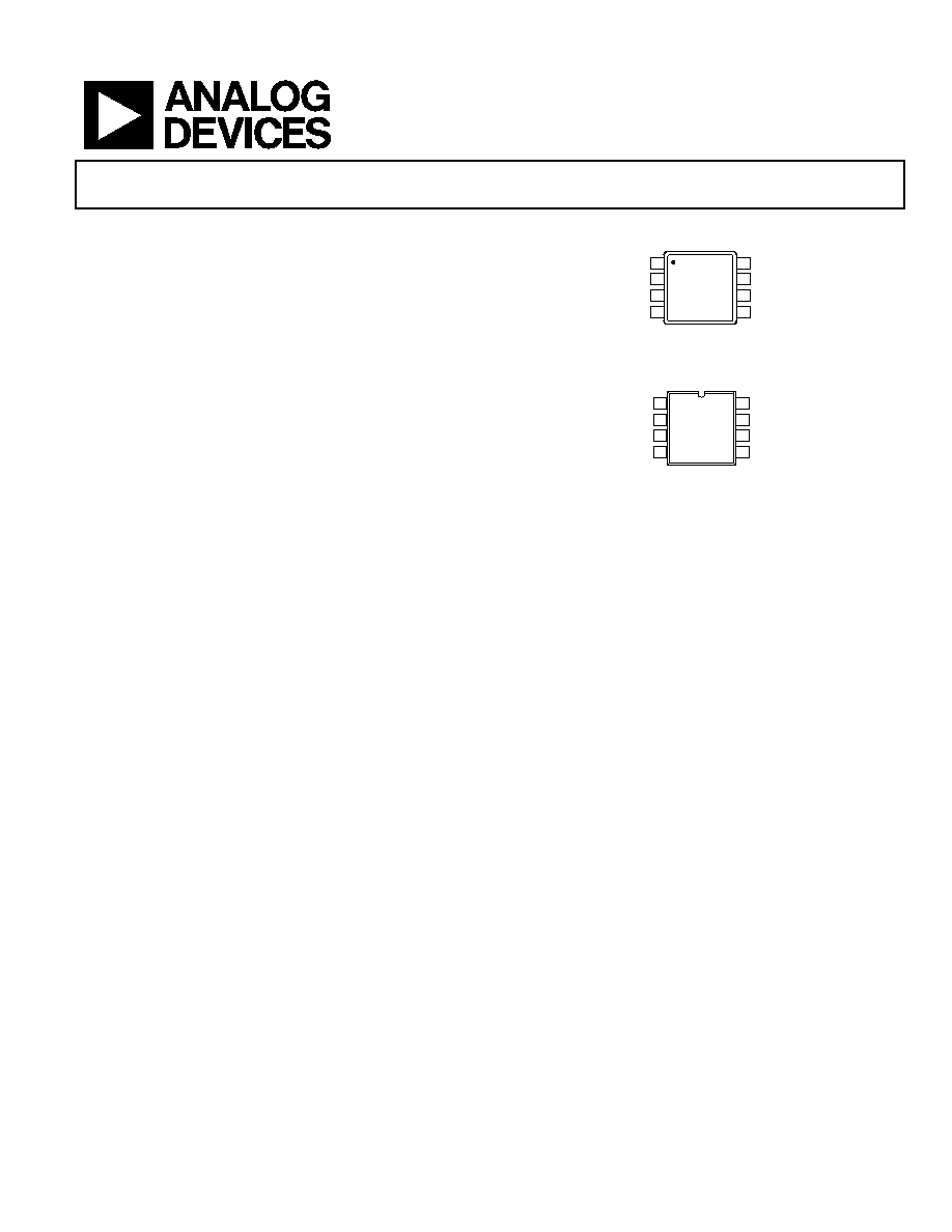
PIN CONFIGURATIONS
OUT A
1
IN A
2
+IN A
3
V
4
V+
8
OUT B
7
IN B
6
+IN B
5
AD8692
TOP VIEW
(Not to Scale)
04991-001
Figure 1. 8-Lead MSOP Pin Configuration
OUT A
1
IN A
2
+IN A
3
V
4
V+
8
OUT B
7
IN B
6
+IN B
5
AD8692
TOP VIEW
(Not to Scale)
04991-002
Figure 2. 8-Lead SOIC Pin Configuration
GENERAL DESCRIPTION
The AD8692 is a low cost, dual rail-to-rail output, single-supply
amplifier featuring low offset voltage, low input voltage and
current noise, and wide signal bandwidth. The combination of
low offset, low noise, very low input bias currents, and high
speed makes this amplifier useful in a wide variety of applica-
tions. Filters, integrators, photodiode amplifiers, and high
impedance sensors all benefit from the combination of
performance features. Audio and other ac applications benefit
from the wide bandwidth and low distortion.
Applications for this amplifier include PA controls, laser diode
control loops, portable and loop-powered instrumentation,
audio amplification for portable devices, and ASIC input and
output amplifiers.
The AD8692 is specified over the extended industrial tempera-
ture range of -40°C to +125°C. The AD8692 is available in the
micro-SOIC and 8-lead narrow SOIC surface-mount packages.

AD8692
Rev. 0 | Page 2 of 12
TABLE OF CONTENTS
Electrical Characteristics ................................................................. 3
Absolute Maximum Ratings............................................................ 5
Thermal Characteristics .............................................................. 5
ESD Caution.................................................................................. 5
Typical Performance Characteristics ..............................................6
Outline Dimensions ....................................................................... 11
Ordering Guide .......................................................................... 11
REVISION HISTORY
10/04--Revision 0: Initial Version

AD8692
Rev. 0 | Page 3 of 12
ELECTRICAL CHARACTERISTICS
V
S
= 2.7 V, V
CM
= V
S
/2, T
A
= 25°C, unless otherwise noted.
Table 1.
Parameter Symbol
Conditions
Min
Typ
Max
Unit
INPUT
CHARACTERISTICS
Offset Voltage
V
OS
V
CM
= -0.3 V to +1.6 V
0.4
2.0
mV
V
CM
= -0.1 V to +1.6 V; -40°C < T
A
< +125°C
3.0
mV
Input Bias Current
I
B
0.2
1
pA
-40°C < T
A
< +85°C
50
pA
-40°C < T
A
< +125°C
260
pA
Input Offset Current
I
OS
0.1
0.5
pA
-40°C < T
A
< +85°C
20
pA
-40°C < T
A
< +125°C
75
pA
Input Voltage Range
-0.3
+1.6
V
Common-Mode Rejection Ratio
CMRR
V
CM
= -0.3 V to +1.6 V
70
90
dB
V
CM
= -0.1 V to +1.6 V; -40°C < T
A
< +125°C
65
85
dB
Large Signal Voltage Gain
A
VO
R
L
= 2 k, V
O
= 0.5 V to 2.2 V
90
250
V/mV
Offset Voltage Drift
V
OS
/T
1.3
6.0 µV/°C
OUTPUT
CHARACTERISTICS
Output Voltage High
V
OH
I
L
= 1 mA
2.64
2.66
V
-40°C < T
A
< +125°C
2.6
V
Output Voltage Low
V
OL
I
L
= 1 mA
25
40
mV
-40°C < T
A
< +125°C
50
mV
Short-Circuit Current
I
SC
±20
mA
Closed-Loop Output Impedance
Z
OUT
f = 1 MHz, A
V
= 1
12
POWER
SUPPLY
Power-Supply Rejection Ratio
PSRR
V
S
= 2.7 V to 5.5 V
80
95
dB
-40°C < T
A
< +125°C
75
95
dB
Supply Current/Amplifier
I
SY
V
O
= 0 V
0.85
0.95
mA
-40°C < T
A
< +125°C
1.2
mA
DYNAMIC
PERFORMANCE
Slew Rate
SR
R
L
= 2 k
5
V/µs
Settling Time
t
S
To
0.01%
1 µs
Gain Bandwidth Product
GBP
10
MHz
Phase
Margin
Øo
60 Degrees
Total Harmonic Distortion + Noise
THD+N
G = 1, R
L
= 600 , f = 1 kHz, V
O
= 250 mV p-p
0.003
%
NOISE PERFORMANCE
Voltage Noise
e
n p-p
f = 0.1 Hz to 10 Hz
1.6
3.0
µV p-p
Voltage Noise Density
e
n
f = 1 kHz
8
12
nV/Hz
e
n
f = 10 kHz
6.5
nV/Hz
Current Noise Density
i
n
f = 1 kHz
0.05
pA/Hz

AD8692
Rev. 0 | Page 4 of 12
V
S
= 5.0 V, V
CM
= V
S
/2, T
A
= 5°C, unless otherwise noted.
Table 2.
A
Grade
Parameter Symbol
Conditions
Min
Typ
Max
Unit
INPUT
CHARACTERISTICS
Offset Voltage
V
OS
V
CM
= -0.3 V to +3.9 V
0.4
2.0
mV
V
CM
= -0.1 V to +3.9 V; -40°C < T
A
< +125°C
3.0
mV
Input Bias Current
I
B
0.2
1
pA
-40°C < T
A
< +85°C
50
pA
-40°C < T
A
< +125°C
260
pA
Input Offset Current
I
OS
0.1
0.5
pA
-40°C < T
A
< +85°C
20
pA
-40°C < T
A
< +125°C
75
pA
Input Voltage Range
-0.3
+3.9
V
Common-Mode Rejection Ratio
CMRR
V
CM
= -0.3 V to +3.9 V
75
95
dB
V
CM
= -0.1 V to +3.9 V; -40°C < T
A
< +125°C
70
95
dB
Large Signal Voltage Gain
A
VO
V
O
= 0.5 V to 4.5 V, R
L
= 2 k, V
CM
= 0 V
250
2,000
V/mV
Offset Voltage Drift
V
OS
/
T
1.3
6
µV/°C
OUTPUT
CHARACTERISTICS
Output Voltage High
V
OH
I
L
= 1 mA
4.96
4.98
V
I
L
= 10 mA
4.7
4.78
V
-40°C to +125°C
4.6
V
Voltage Low
V
OL
I
L
= 1 mA
16.5
40
mV
I
L
= 10 mA
165
210
mV
-40°C to +125°C
290
mV
Short-Circuit Current
I
SC
±80 mA
Closed-Loop Output Impedance
Z
OUT
f = 1 MHz, A
V
= 1
10
POWER
SUPPLY
Power-Supply Rejection Ratio
PSRR
V
S
= 2.7 V to 5.5 V
80
95
dB
-40°C < T
A
< +125°C
75
95
dB
Supply Current/Amplifier
I
SY
V
O
= 0 V
0.95
1.05
mA
-40°C < T
A
< +125°C
1.3
mA
DYNAMIC
PERFORMANCE
Slew Rate
SR
R
L
= 2 k
5
V/µs
Settling Time
t
S
To
0.01%
1
µs
Full Power Bandwidth
BW
P
<1%
distortion
360 kHz
Gain Bandwidth Product
GBP
10
MHz
Phase
Margin
Øo
65 Degrees
Total Harmonic Distortion + Noise
THD+N
G = 1, R
L
= 600 , f = 1 kHz, V
O
= 1 V p-p
0.0006
%
NOISE
PERFORMANCE
Voltage Noise
e
n p-p
f = 0.1 Hz to 10 Hz
1.6
3.0
µV p-p
Voltage Noise Density
e
n
f = 1 kHz
8
12
nV/
Hz
e
n
f = 10 kHz
6.5
nV/
Hz
Current Noise Density
i
n
f = 1 kHz
0.05
pA/
Hz
AD8692
Rev. 0 | Page 5 of 12
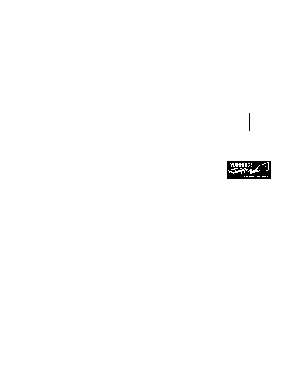
ABSOLUTE MAXIMUM RATINGS
T
A
= 25°C, unless otherwise noted.
Table 3.
Parameters Ratings
Supply Voltage
6 V
Input Voltage
V
SS
- 0.3 V to V
DD
+ 0.3 V
Differential Input Voltage
±6 V
Output Short-Circuit Duration to Gnd
1
Observe derating curves
Storage Temperature Range
-65°C to +150°C
Operating Temperature Range
-40°C to +125°C
Junction Temperature Range
-65°C to +150°C
Lead Temperature Range
(Soldering, 60 s)
300°C
1
JA
is specified for the worst-case conditions, that is, the device soldered in
the circuit board for surface-mount packages.
Stresses above those listed under Absolute Maximum Ratings
may cause permanent damage to the device. This is a stress
rating only and functional operation of the device at these or
any other conditions above those indicated in the operational
section of this specification is not implied. Exposure to absolute
maximum rating conditions for extended periods may affect
device reliability.
THERMAL CHARACTERISTICS
Table 4.
Package Type
JA
JC
Unit
8-Lead MSOP (RM)
210
45
°C/W
8-Lead SOIC (R)
158
43
°C/W
ESD CAUTION
ESD (electrostatic discharge) sensitive device. Electrostatic charges as high as 4000 V readily accumulate on
the human body and test equipment and can discharge without detection. Although this product features
proprietary ESD protection circuitry, permanent damage may occur on devices subjected to high energy
electrostatic discharges. Therefore, proper ESD precautions are recommended to avoid performance
degradation or loss of functionality.
AD8692
Rev. 0 | Page 6 of 12
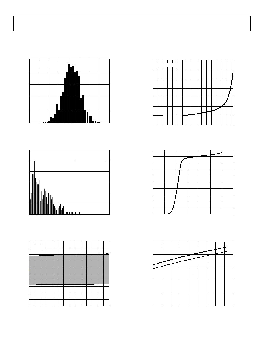
TYPICAL PERFORMANCE CHARACTERISTICS
V
S
= +5 V or ±2.5 V.
NUMBE
R OF AMP
L
IFIE
RS
V
OS
(mV)
04991-003
0
500
1.0k
1.5k
2.0k
2.5k
2.0
1.5
1.0
0.5
0
0.5
1.0
1.5
2.0
V
S
= 5V
V
CM
= 0.3V TO +3.9V
Figure 3. Input Offset Voltage Distribution
NUMBE
R OF AMP
L
IFIE
RS
T
C
V
OS
(
µV/°C)
04991-004
0
5
10
15
20
25
30
V
S
= 5V AND 2.7V
V
CM
= 2.5V
T
A
= 40
°C TO +125°C
4.0 4.5 5.0 5.5 6.0 6.5 7.0 7.5 8.0
0
0.5 1.0 1.5 2.0 2.5 3.0 3.5
Figure 4. Input Offset Voltage Drift Distribution
2.0k
1.6k
1.2k
800
400
0
400
800
1.2k
1.6k
2.0k
IN
PU
T OFFSET VOLTA
GE (
µ
V)
0.3 0
0.3 0.6 0.9 1.2
1.8
3.0
1.5
2.1 2.4 2.7
3.6
3.3
3.9
COMMON-MODE VOLTAGE (V)
04991-005
V
S
= 5V
T
A
= 25
°C
Figure 5. Input Offset Voltage vs. Common-Mode Voltage
IB (
p
A)
TEMPERATURE (
°C)
04991-006
50
0
50
100
150
200
250
300
IB (
p
A)
40
20
0
20
40
60
80
100
120
10
10
30
50
70
90
110
30
V
S
= 5V AND 2.7V
Figure 6. Input Bias Current vs. Temperature
0
0.2
0.4
0.6
0.8
1.0
1.2
1.4
1.6
1.8
2.0
I
SY
(mA)
0
1
2
3
4
5
6
7
V
SY
(V)
04991-007
Figure 7. Supply Current vs. Supply Voltage
0
0.5
1.0
1.5
2.0
2.5
S
U
P
P
L
Y
CURRE
NT (mA)
40
20
0
20
40
60
80
100
120
140
TEMPERATURE (
°C)
04991-008
V
S
=
±2.5V AND ±1.35V
I
SY
@
±2.5V
I
SY
@
±1.35V
Figure 8. Supply Current vs. Temperature
AD8692
Rev. 0 | Page 7 of 12
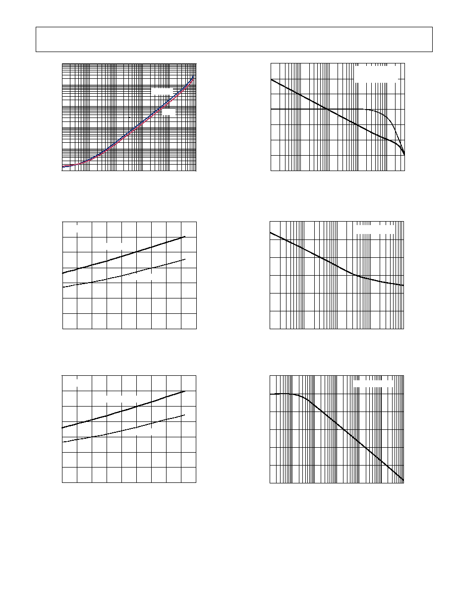
0.1
1
10
100
1k
10k
0.001
0.01
0.1
1
10
100
OU
TPU
T
VOLTA
G
E TO SU
PPLY R
A
IL (
m
V)
LOAD CURRENT (mA)
04991-009
SOURCE
SINK
Figure 9. Output Voltage to Supply Rail vs. Load Current
0
5
10
15
20
25
30
35
OU
TPU
T
VOLTA
GE SW
IN
G (
m
V)
40
20
0
20
40
60
80
100
120
140
TEMPERATURE (
°C)
04991-010
V
S
= 5V
V
DD
V
OH
@ 1mA
V
OL
@ 1mA
Figure 10. Output Voltage Swing vs. Temperature
(IL = 1 mA)
0
50
100
150
200
250
300
350
OUTPUT VOLTAGE SW
ING (mV)
40
20
0
20
40
60
80
100
120
140
TEMPERATURE (
°C)
04991-011
V
S
= 5V
V
DD
V
OH
@ 10mA
V
OL
@ 10mA
Figure 11. Output Voltage Swing vs. Temperature
(IL = 10 mA)
1k
10k
100k
1M
10M
OPEN-LOOP GAIN (dB)
FREQUENCY (Hz)
04991-012
40
20
20
40
60
80
100
0
PH
A
SE (
D
egrees)
90
45
45
90
0
V
SY
=
±2.5V, ±1.35V
R
L
= 2k
C
L
= 15pF
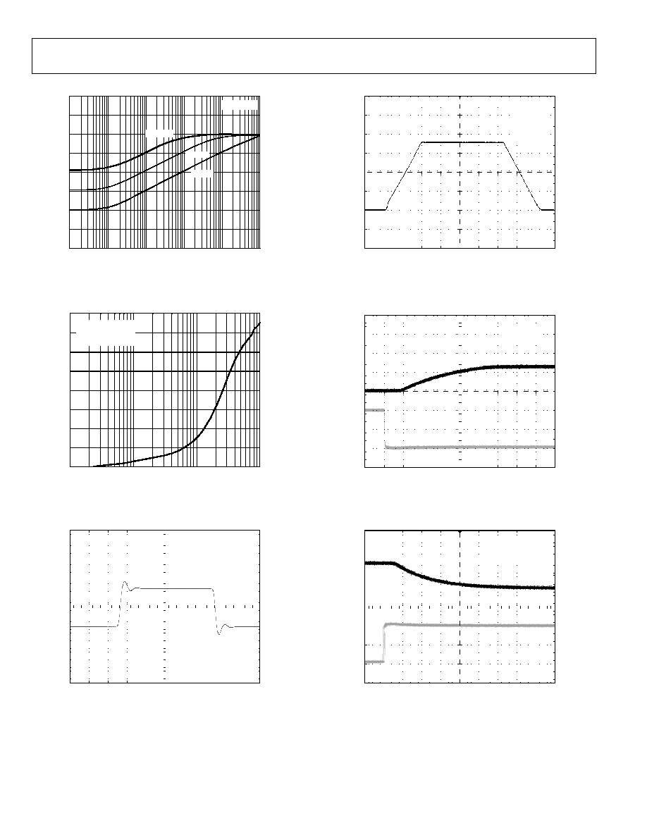
Figure 12. Open-Loop Gain and Phase vs. Frequency
1k
10k
100k
1M
10M
CMRR (dB)
FREQUENCY (Hz)
04991-013
0
40
60
80
100
120
20
V
S
= 5V AND 2.7V
Figure 13. CMRR vs. Frequency
P
S
RR (dB)
FREQUENCY (Hz)
04991-014
0
40
60
80
100
120
20
10
100
1k
10k
100k
1M
10M
V
S
= 5V AND 2.7V
Figure 14. PSRR vs. Frequency
AD8692
Rev. 0 | Page 8 of 12
0.0001
0.001
0.01
0.1
1
10
100
1k
10k
100
1k
10k
100k
1M
10M
IMP
E
DANCE
(
)
FREQUENCY (Hz)
04991-015
V
S
=
±2.5V
A
V
= 100
A
V
= 10
A
V
= 1
Figure 15. Closed-Loop Output Impedance vs. Frequency
OVER
SH
OOT (
%
)
1
10
100
1k
LOAD CAPACITANCE (pF)
04991-016
0
5
10
15
20
25
30
35
40
V
S
= 5V AND 2.7V
R
L
=
A
V
= 1
Figure 16. Small Signal Overshoot vs. Load Capacitance
VOLTA
GE (
50mV/D
I
V)
TIME (200ns/DIV)
04991-017
V
S
=
±2.5V, ±1.35V
R
L
= 10k
C
L
= 200pF
A
V
= 1
Figure 17. Small Signal Transient Response
VOLTA
GE (
1
V/D
I
V)
TIME (400nV/DIV)
04991-018
V
S
= 5V
C
L
= 200pF
R
L
=
A
V
= 1
Figure 18. Large Signal Transient Response
V
OUT
(V
)
TIME (400ns/DIV)
04991-019
V
S
=
±2.5V
A
V
= 50
2.5
100
0
0
V
IN
(mV
)
Figure 19. Positive Overload Recovery
V
OUT
(V
)
TIME (400ns/DIV)
04991-020
V
S
=
±2.5V
A
V
= 50
2.5
100
0
0
V
IN
(mV
)
Figure 20. Negative Overload Recovery
AD8692
Rev. 0 | Page 9 of 12
0.0001
0.001
0.01
THD + N (%)
20
100
1k
10k
20k
FREQUENCY (Hz)
04991-021
0.1
V
S
=
±2.5V
A
V
= 1
V
IN
= 1V p-p
BW = 20kHz
R
L
= 1k
R
L
= 600
R
L
= 100k
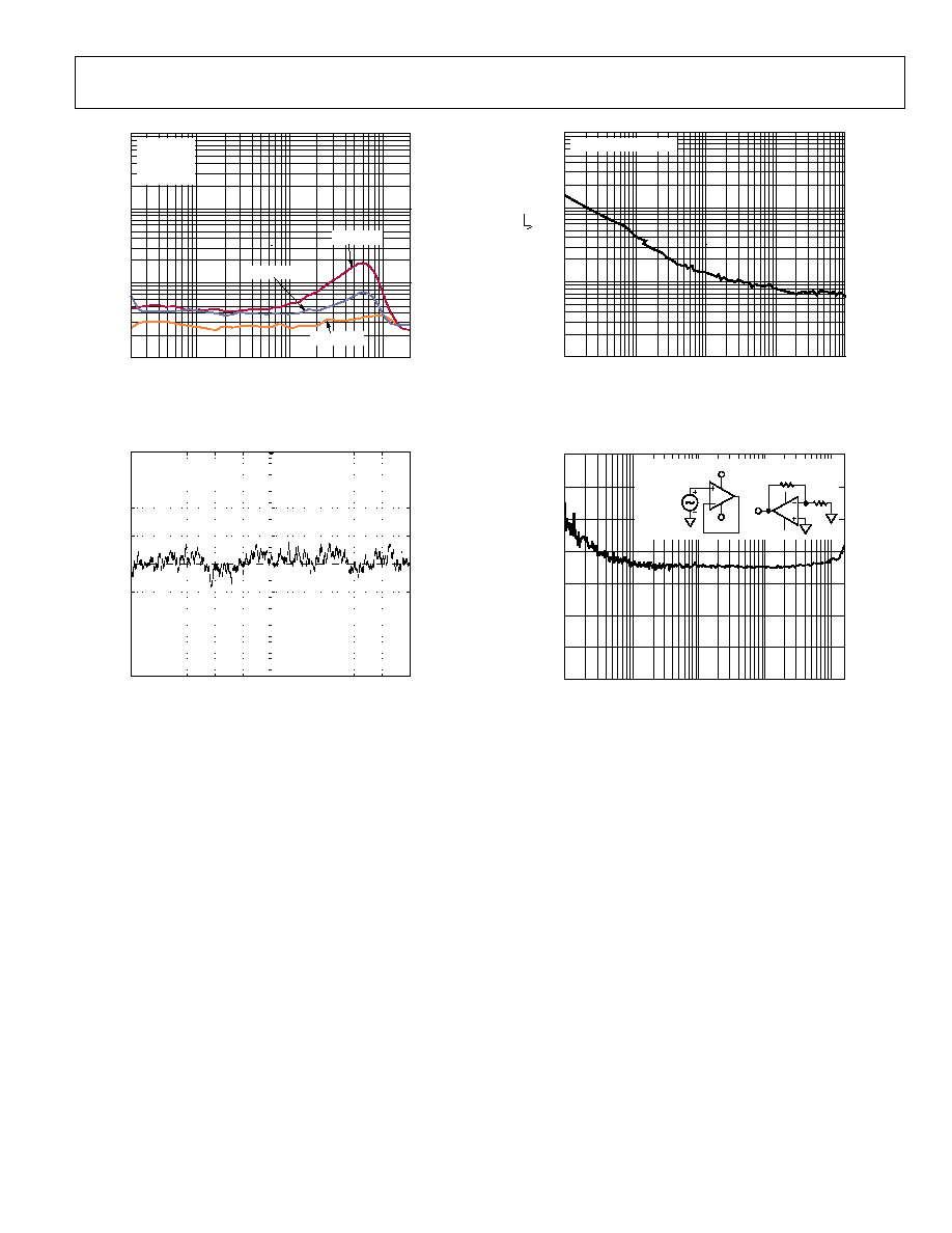
Figure 21. THD + N vs. Frequency
VOLTA
GE N
O
ISE (
1
µ
V/D
I
V)
TIME (1s/DIV)
04991-022
V
S
= 5V AND 2.7V
Figure 22. 0.1 Hz to 10 Hz Input Voltage Noise
N
O
ISE (
n
V/ H
z
)
1
100
10
1k
FREQUENCY (Hz)
10
1
100
1k
10k
04991-023
V
S
=
±2.5V AND ±1.35V
Figure 23. Voltage Noise Density
1k
10k
100k
1M
10M
CHANNEL SEPARATION (dB)
FREQUENCY (Hz)
04991-024
80
90
110
120
130
140
150
100
V
IN
28mV p-p
V
2.5V
V+
+2.5V
A
B
V
OUT
V+
V
R1
10k
R2
100
Figure 24. Channel Separation
AD8692
Rev. 0 | Page 10 of 12
V
S
= +2.7 V or ±1.35 V.
NUM
B
ER OF AM
PLIFIERS
V
OS
(mV)
04991-025
0
200
400
600
800
1.0k
1.2k
2.0
1.5
1.0
0.5
0
0.5
1.0
1.5
2.0
V
S
= 2.7V
V
CM
= 0.3V TO +1.6V
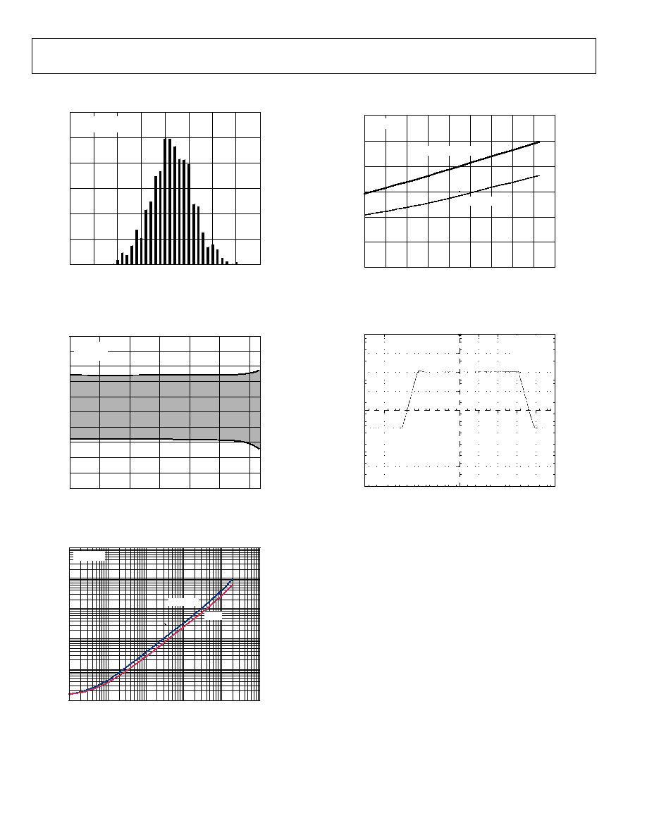
Figure 25. Input Offset Voltage Distribution
INPUT OFFSET VOLTAGE (
µ
V)
COMMON-MODE VOLTAGE (V)
04991-026
2.0k
1.6k
1.2k
800
400
400
800
1.2k
1.6k
2.0k
0.3
0
0.3
0.6
0.9
1.2
1.5 1.6
0
V
S
= 2.7V
T
A
= 25
°C
Figure 26. Input Offset Voltage vs. Common-Mode Voltage
0.1
1
10
100
1k
10k
0.001
0.01
0.1
1
10
100
OU
TPU
T
VOLTA
GE TO SU
PPLY R
A
I
L (
m
V)
LOAD CURRENT (mA)
04991-027
SOURCE
SINK
V
S
= 2.7V
Figure 27. Output Voltage to Supply Rail vs. Load Current
0
10
20
30
40
50
60
OU
TPU
T
VOLTA
GE SW
IN
G (
m
V)
40
20
0
20
40
60
80
100
120
140
TEMPERATURE (
°C)
04991-028
V
S
= 2.7V
V
DD
V
OH
@ 1mA
V
OL
@ 1mA
Figure 28. Output Voltage Swing vs. Temperature
VOLTA
GE (
500mV/D
I
V)
TIME (400ns/DIV)
04991-029
V
S
= 2.7V
C
L
= 200pF
R
L
=
A
V
= 1
Figure 29. Large Signal Transient Response
AD8692
Rev. 0 | Page 11 of 12
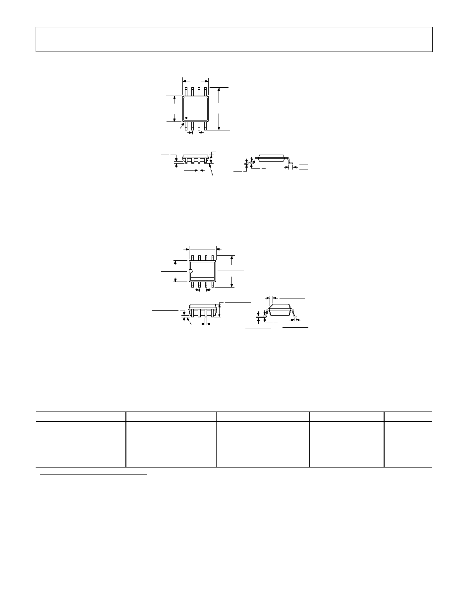
OUTLINE DIMENSIONS
0.80
0.60
0.40
8°
0°
4
8
5
4.90
BSC
PIN 1
0.65 BSC
3.00
BSC
SEATING
PLANE
0.15
0.00
0.38
0.22
1.10 MAX
3.00
BSC
COPLANARITY
0.10
0.23
0.08
COMPLIANT TO JEDEC STANDARDS MO-187AA
Figure 30. 8-Lead Mini Small Outline Package [MSOP]
(RM-8)
Dimensions shown in millimeters
0.25 (0.0098)
0.17 (0.0067)
1.27 (0.0500)
0.40 (0.0157)
0.50 (0.0196)
0.25 (0.0099)
× 45°
8°
0°
1.75 (0.0688)
1.35 (0.0532)
SEATING
PLANE
0.25 (0.0098)
0.10 (0.0040)
4
1
8
5
5.00 (0.1968)
4.80 (0.1890)
4.00 (0.1574)
3.80 (0.1497)
1.27 (0.0500)
BSC
6.20 (0.2440)
5.80 (0.2284)
0.51 (0.0201)
0.31 (0.0122)
COPLANARITY
0.10
CONTROLLING DIMENSIONS ARE IN MILLIMETERS; INCH DIMENSIONS
(IN PARENTHESES) ARE ROUNDED-OFF MILLIMETER EQUIVALENTS FOR
REFERENCE ONLY AND ARE NOT APPROPRIATE FOR USE IN DESIGN
COMPLIANT TO JEDEC STANDARDS MS-012AA
Figure 31. 8-Lead Standard Small Outline Package [SOIC]
(R-8)
Dimensions shown in millimeters and (inches)
ORDERING GUIDE
Model
Temperature Range
Package Description Package
Option
Branding
AD8692ARMZ-R2
1
-40°C to +125°C
8-Lead MSOP
RM-8
APA
AD8692ARMZ-REEL
1
-40°C to +125°C
8-Lead MSOP
RM-8
APA
AD8692ARZ
1
-40°C to +125°C
8-Lead SOIC
R-8
AD8692ARZ-REEL
1
-40°C to +125°C
8-Lead SOIC
R-8
AD8692ARZ-REEL7
1
-40°C to +125°C
8-Lead SOIC
R-8
1
Z = Pb-free part.

AD8692
Rev. 0 | Page 12 of 12
NOTES
© 2004 Analog Devices, Inc. All rights reserved. Trademarks and
registered trademarks are the property of their respective owners.
D04991010/04(0)
Document Outline