 | ÐлекÑÑоннÑй компоненÑ: AD9222 | СкаÑаÑÑ:  PDF PDF  ZIP ZIP |
Äîêóìåíòàöèÿ è îïèñàíèÿ www.docs.chipfind.ru
Octal, 12-Bit, 40/50 MSPS
Serial LVDS 1.8 V A/D Converter
AD9222
Rev. 0
Information furnished by Analog Devices is believed to be accurate and reliable. However, no
responsibility is assumed by Analog Devices for its use, nor for any infringements of patents or other
rights of third parties that may result from its use. Specifications subject to change without notice. No
license is granted by implication or otherwise under any patent or patent rights of Analog Devices.
Trademarks and registered trademarks are the property of their respective owners.
One Technology Way, P.O. Box 9106, Norwood, MA 02062-9106, U.S.A.
Tel: 781.329.4700
www.analog.com
Fax: 781.461.3113
©2006 Analog Devices, Inc. All rights reserved.
FEATURES
8 ADCs integrated into 1 package
93 mW ADC power per channel at 50 MSPS
SNR = 70 dB (to Nyquist)
ENOB = 11.3 bits
SFDR = 84 dBc
Excellent linearity
DNL = ±0.3 LSB (typical)
INL = ±0.4 LSB (typical)
Serial LVDS (ANSI-644, default)
Low power reduced signal option, IEEE 1596.3 similar
Data and frame clock outputs
325 MHz full power analog bandwidth
2 V p-p input voltage range
1.8 V supply operation
Serial port control
Full-chip and individual-channel power-down modes
Flexible bit orientation
Built-in and custom digital test pattern generation
Programmable clock and data alignment
Programmable output resolution
Standby mode
APPLICATIONS
Medical imaging and nondestructive ultrasound
Portable ultrasound and digital beam forming systems
Quadrature radio receivers
Diversity radio receivers
Tape drives
Optical networking
Test equipment
GENERAL DESCRIPTION
The AD9222 is an octal, 12-bit, 40/50 MSPS analog-to-digital
converter (ADC) with an on-chip sample-and-hold circuit that
is designed for low cost, low power, small size, and ease of use.
The product operates at a conversion rate of up to 50 MSPS and
is optimized for outstanding dynamic performance and low
power in applications where a small package size is critical.
The ADC requires a single 1.8 V power supply and LVPECL-/
CMOS-/LVDS-compatible sample rate clock for full performance
operation. No external reference or driver components are
required for many applications.
The ADC automatically multiplies the sample rate clock for
the appropriate LVDS serial data rate. A data clock (DCO)
for capturing data on the output and a frame clock (FCO) for
signaling a new output byte are provided. Individual channel
power-down is supported and typically consumes less than
2 mW when all channels are disabled.
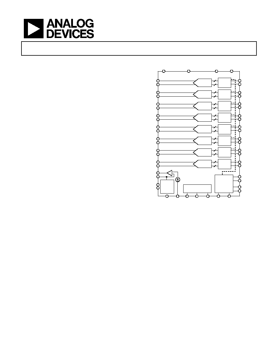
FUNCTIONAL BLOCK DIAGRAM
SERIAL
LVDS
REF
SELECT
AD9222
AGND
VINA
VIN+A
VINB
VIN+B
VIND
VIN+D
VINC
VIN+C
SENSE
VREF
AVDD
DRVDD
12
12
12
12
PDWN
REFT
REFB
DA
D+A
DB
D+B
DD
D+D
DC
D+C
FCO
FCO+
DCO+
DCO
CLK+
DRGND
CLK
SERIAL PORT
INTERFACE
CSB
SCLK/
DTP
SDIO/
ODM
RBIAS
SERIAL
LVDS
SERIAL
LVDS
SERIAL
LVDS
ADC
ADC
ADC
ADC
DATA RATE
MULTIPLIER
0.5V
SERIAL
LVDS
VINE
VIN+E
VINF
VIN+F
VINH
VIN+H
VING
VIN+G
12
12
12
12
DE
D+E
DF
D+F
DH
D+H
DG
D+G
SERIAL
LVDS
SERIAL
LVDS
SERIAL
LVDS
ADC
ADC
ADC
ADC
0
5967-
0
01
Figure 1.
The ADC contains several features designed to maximize
flexibility and minimize system cost, such as programmable
clock and data alignment and programmable digital test pattern
generation. The available digital test patterns include built-in
deterministic and pseudorandom patterns, along with custom user-
defined test patterns entered via the serial port interface (SPI®).
The AD9222 is available in a Pb-free, 64-lead LFCSP package. It is
specified over the industrial temperature range of -40°C to +85°C.
PRODUCT HIGHLIGHTS
1. Small Footprint. Eight ADCs are contained in a small, space-
saving package; low power of 93 mW/channel at 50 MSPS.
2. Ease of Use. A data clock output (DCO) operates up to
300 MHz and supports double data rate operation (DDR).
3. User Flexibility. Serial port interface (SPI) control offers a wide
range of flexible features to meet specific system requirements.
4. Pin-Compatible Family. This includes the AD9212 (10-bit),
and AD9252 (14-bit).

AD9222
Rev. 0 | Page 2 of 56
TABLE OF CONTENTS
Features .............................................................................................. 1
Applications....................................................................................... 1
General Description ......................................................................... 1
Functional Block Diagram .............................................................. 1
Product Highlights ........................................................................... 1
Revision History ............................................................................... 2
Specifications..................................................................................... 3
AC Specifications.......................................................................... 4
Digital Specifications ................................................................... 5
Switching Specifications .............................................................. 6
Timing Diagrams.............................................................................. 7
Absolute Maximum Ratings............................................................ 9
Thermal Impedance ..................................................................... 9
ESD Caution.................................................................................. 9
Pin Configuration and Function Descriptions........................... 10
Equivalent Circuits ......................................................................... 12
Typical Performance Characteristics ........................................... 14
Theory of Operation ...................................................................... 18
Analog Input Considerations ................................................... 18
Clock Input Considerations...................................................... 21
Serial Port Interface (SPI).............................................................. 29
Hardware Interface..................................................................... 30
Memory Map .................................................................................. 32
Reading the Memory Map Table.............................................. 32
Reserved Locations .................................................................... 32
Default Values ............................................................................. 32
Logic Levels................................................................................. 32
Evaluation Board ............................................................................ 36
Power Supplies ............................................................................ 36
Input Signals................................................................................ 36
Output Signals ............................................................................ 36
Default Operation and Jumper Selection Settings................. 37
Alternative Analog Input Drive Configuration...................... 38
Outline Dimensions ....................................................................... 55
Ordering Guide .......................................................................... 55
REVISION HISTORY
9/06--Revision 0: Initial Version

AD9222
Rev. 0 | Page 3 of 56
SPECIFICATIONS
AVDD = 1.8 V, DRVDD = 1.8 V, 2 V p-p differential input, 1.0 V internal reference, AIN = -0.5 dBFS, unless otherwise noted.
Table 1.
AD9222-40
AD9222-50
Parameter
1
Temperature Min Typ
Max Min Typ
Max Unit
RESOLUTION
12
12
Bits
ACCURACY
No Missing Codes
Full
Guaranteed
Guaranteed
Offset Error
Full
±1
±8
±1
±8
mV
Offset Matching
Full
±3
±8
±3
±8
mV
Gain Error
Full
±0.4
±1.2
±1.5
±2.5
% FS
Gain Matching
Full
±0.3
±0.7
±0.3
±0.7
% FS
Differential Nonlinearity (DNL)
Full
±0.25
±0.5
±0.3
±0.65
LSB
Integral Nonlinearity (INL)
Full
±0.4
±1
±0.4
±1
LSB
TEMPERATURE DRIFT
Offset Error
Full
±2
±2
ppm/°C
Gain Error
Full
±17
±17
ppm/°C
Reference Voltage (1 V Mode)
Full
±21
±21
ppm/°C
REFERENCE
Output Voltage Error (VREF = 1 V)
Full
±2
±30
±2
±30
mV
Load Regulation @ 1.0 mA (VREF = 1 V)
Full
3
3
mV
Input Resistance
Full
6
6
k
ANALOG INPUTS
Differential Input Voltage Range (VREF = 1 V)
Full
2
2
V p-p
Common-Mode Voltage
Full
AVDD/2
AVDD/2
V
Differential Input Capacitance
Full
7
7
pF
Analog Bandwidth, Full Power
Full
325
325
MHz
POWER SUPPLY
AVDD Full
1.7
1.8
1.9
1.7
1.8
1.9
V
DRVDD Full
1.7
1.8
1.9
1.7
1.8
1.9
V
IAVDD Full
338
348.5
357.5
367.5
mA
IDRVDD Full
51
53.6
53.5
56.2
mA
Total Power Dissipation (Including Output Drivers)
Full
700
722
740
760
mW
Power-Down Dissipation
Full
2
11
2
11
mW
Standby Dissipation
2
Full
83
89
mW
CROSSTALK Full
-90
-90
dB
CROSSTALK (Overrange Condition)
3
Full
-90
-90
dB
1
See the AN-835 Application Note, Understanding High Speed ADC Testing and Evaluation, for a complete set of definitions and how these tests were completed.
2
Can be controlled via SPI.
3
Overrange condition is specific with 6 dB of the full-scale input range.

AD9222
Rev. 0 | Page 4 of 56
AC SPECIFICATIONS
AVDD = 1.8 V, DRVDD = 1.8 V, 2 V p-p differential input, 1.0 V internal reference, AIN = -0.5 dBFS, unless otherwise noted.
Table 2.
AD9222-40
AD9222-50
Parameter
1
Temperature
Min Typ Max
Min Typ Max
Unit
SIGNAL-TO-NOISE RATIO (SNR)
f
IN
= 2.4 MHz
Full
70.3
70.4
dB
f
IN
= 19.7 MHz
Full
69.5
70.3
69.5
70.3
dB
f
IN
= 35 MHz
Full
69.9
70.0
dB
f
IN
= 70 MHz
Full
68.8
69.0
dB
SIGNAL-TO-NOISE AND DISTORTION RATIO (SINAD)
f
IN
= 2.4 MHz
Full
70.0
70.0
dB
f
IN
= 19.7 MHz
Full
68.7
70.0
68.5
70.0
dB
f
IN
= 35 MHz
Full
69.5
69.8
dB
f
IN
= 70 MHz
Full
68.0
68.5
dB
EFFECTIVE NUMBER OF BITS (ENOB)
f
IN
= 2.4 MHz
Full
11.38
11.4
Bits
f
IN
= 19.7 MHz
Full
11.25
11.38
11.25
11.38
Bits
f
IN
= 35 MHz
Full
11.32
11.33
Bits
f
IN
= 70 MHz
Full
11.14
11.17
Bits
SPURIOUS-FREE DYNAMIC RANGE (SFDR)
f
IN
= 2.4 MHz
Full
85
85
dBc
f
IN
= 19.7 MHz
Full
73
85
73
84
dBc
f
IN
= 35 MHz
Full
80
83
dBc
f
IN
= 70 MHz
Full
76
77
dBc
WORST HARMONIC (Second or Third)
f
IN
= 2.4 MHz
Full
-85
-85
dBc
f
IN
= 19.7 MHz
Full
-85
-74
-84
-73
dBc
f
IN
= 35 MHz
Full
-80
-83
dBc
f
IN
= 70 MHz
Full
-76
-77
dBc
WORST OTHER (Excluding Second or Third)
f
IN
= 2.4 MHz
Full
-92
-92
dBc
f
IN
= 19.7 MHz
Full
-92
-80
-92
-80
dBc
f
IN
= 35 MHz
Full
-92
-92
dBc
f
IN
= 70 MHz
Full
-90
-90
dBc
TWO-TONE INTERMODULATION DISTORTION (IMD)--
AIN1 AND AIN2 = -7.0 dBFS
f
IN1
= 15 MHz,
f
IN2
= 16 MHz
25°C
80.0
80.0
dBc
f
IN1
= 70 MHz,
f
IN2
= 71 MHz
25°C
77.0
77.0
dBc
1
See the AN-835 Application Note, Understanding High Speed ADC Testing and Evaluation, for a complete set of definitions and how these tests were completed.

AD9222
Rev. 0 | Page 5 of 56
DIGITAL SPECIFICATIONS
AVDD = 1.8 V, DRVDD = 1.8 V, 2 V p-p differential input, 1.0 V internal reference, AIN = -0.5 dBFS, unless otherwise noted.
Table 3.
AD9222-40
AD9222-50
Parameter
1
Temperature Min Typ Max
Min Typ Max
Unit
CLOCK INPUTS (CLK+, CLK-)
Logic Compliance
CMOS/LVDS/LVPECL
CMOS/LVDS/LVPECL
Differential Input Voltage
2
Full
250
250
mV
p-p
Input
Common-Mode
Voltage
Full
1.2
1.2
V
Input
Resistance
(Differential)
25°C
20
20
k
Input
Capacitance
25°C
1.5
1.5
pF
LOGIC INPUTS (PDWN, SCLK/DTP)
Logic
1
Voltage
Full
1.2
3.6
1.2
3.6
V
Logic
0
Voltage
Full
0 0.3
0.3
V
Input
Resistance
25°C
30
30
k
Input
Capacitance
25°C
0.5
0.5
pF
LOGIC
INPUT
(CSB)
Logic
1
Voltage
Full
1.2
3.6
1.2
3.6
V
Logic
0
Voltage
Full
0 0.3
0.3
V
Input
Resistance
25°C
70
70
k
Input
Capacitance
25°C
0.5
0.5
pF
LOGIC
INPUT
(SDIO/ODM)
Logic 1 Voltage
Full
1.2
DRVDD + 0.3
1.2
DRVDD + 0.3
V
Logic
0
Voltage
Full
0 0.3
0 0.3
V
Input
Resistance
25°C
30
30
k
Input
Capacitance
25°C
2
2
pF
LOGIC OUTPUT (SDIO/ODM)
3
Logic 1 Voltage (I
OH
= 800 A)
Full
1.79
1.79
V
Logic 0 Voltage (I
OL
= 50 A)
Full
0.05
0.05
V
DIGITAL OUTPUTS (D+, D-), (ANSI-644)
1
Logic
Compliance
LVDS
LVDS
Differential Output Voltage (V
OD
)
Full
247
454
247
454
mV
Output Offset Voltage (V
OS
)
Full
1.125
1.375
1.125
1.375
V
Output Coding (Default)
Offset binary
Offset binary
DIGITAL OUTPUTS (D+, D-),
(Low Power, Reduced Signal Option)
1
Logic
Compliance
LVDS
LVDS
Differential Output Voltage (V
OD
)
Full
150
250
150
250
mV
Output Offset Voltage (V
OS
)
Full
1.10
1.30
1.10
1.30
V
Output Coding (Default)
Offset binary
Offset binary
1
See the AN-835 Application Note, Understanding High Speed ADC Testing and Evaluation, for a complete set of definitions and how these tests were completed.
2
This is specified for LVDS and LVPECL only.
3
This is specified for 13 SDIO pins sharing the same connection.

AD9222
Rev. 0 | Page 6 of 56
SWITCHING SPECIFICATIONS
AVDD = 1.8 V, DRVDD = 1.8 V, 2 V p-p differential input, 1.0 V internal reference, AIN = -0.5 dBFS, unless otherwise noted.
Table 4.
AD9222-40 AD9222-50
Parameter
1
Temp
Min
Typ Max
Min
Typ Max
Unit
CLOCK
2
Maximum
Clock
Rate
Full
40
50
MSPS
Minimum Clock Rate
Full
10
10
MSPS
Clock Pulse Width High (t
EH
)
Full
12.5
10.0
ns
Clock Pulse Width Low (t
EL
)
Full
12.5
10.0
ns
OUTPUT PARAMETERS
2
, 3
Propagation Delay (t
PD
)
Full
1.5
2.3 3.1
1.5
2.3 3.1
ns
Rise Time (t
R
) (20% to 80%)
Full
300
300
ps
Fall Time (t
F
) (20% to 80%)
Full
300
300
ps
FCO Propagation Delay (t
FCO
)
Full
1.5
2.3 3.1
1.5
2.3 3.1
ns
DCO Propagation Delay (t
CPD
)
4
Full
t
FCO
+
(t
SAMPLE
/24)
t
FCO
+
(t
SAMPLE
/24)
ns
DCO to Data Delay (t
DATA
)
4
Full (t
SAMPLE
/24) - 300
(t
SAMPLE
/24) (t
SAMPLE
/24) + 300
(t
SAMPLE
/24) - 300
(t
SAMPLE
/24) (t
SAMPLE
/24) + 300
ps
DCO to FCO Delay (t
FRAME
)
4
Full (t
SAMPLE
/24) - 300
(t
SAMPLE
/24) (t
SAMPLE
/24) + 300
(t
SAMPLE
/24) - 300
(t
SAMPLE
/24) (t
SAMPLE
/24) + 300
ps
Data to Data Skew
(t
DATA-MAX
- t
DATA-MIN
)
Full
±50 ±200
±50 ±200
ps
Wake-Up Time (Standby)
25°C
600
600
ns
Wake-Up Time (Power Down)
25°C
375
375
s
Pipeline
Latency
Full
8
8
CLK
cycles
APERTURE
Aperture Delay (t
A
)
25°C
750
750
ps
Aperture Uncertainty (Jitter)
25°C
<1
<1
ps
rms
Out-of-Range Recovery Time
25°C
1
1
CLK
cycles
1
See the AN-835 Application Note, Understanding High Speed ADC Testing and Evaluation, for a complete set of definitions and how these tests were completed.
2
Can be adjusted via the SPI interface.
3
Measurements were made using a part soldered to FR4 material.
4
t
SAMPLE
/24 is based on the number of bits divided by 2 because the delays are based on half duty cycles.
AD9222
Rev. 0 | Page 7 of 56
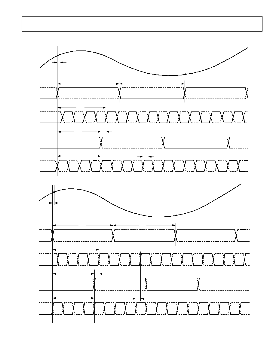
TIMING DIAGRAMS
DCO
DCO+
D
D+
FCO
FCO+
AIN
CLK
CLK+
MSB
N 8
D10
N 8
D9
N 8
D8
N 8
D7
N 8
D6
N 8
D5
N 8
D4
N 8
D3
N 8
D2
N 8
D1
N 8
D0
N 8
D10
N 7
MSB
N 7
N 1
N
t
DATA
t
FRAME
t
FCO
t
PD
t
CPD
t
EH
t
A
t
EL
0
59
67
-
0
02
Figure 2. 12-Bit Data Serial Stream (Default)
DCO+
DCO
CLK+
FCO+
FCO
D
D+
CLK
AIN
MSB
N 8
N 1
N
D8
N 8
D7
N 8
D5
N 8
t
DATA
t
FRAME
t
FCO
t
PD
D4
N 8
D6
N 8
D8
N 7
D7
N 7
D5
N 7
D6
N 7
D3
N 8
D1
N 8
MSB
N 7
D0
N 8
D2
N 8
t
CPD
t
EH
t
A
t
EL
0
59
67
-
0
03
Figure 3. 10-Bit Data Serial Stream
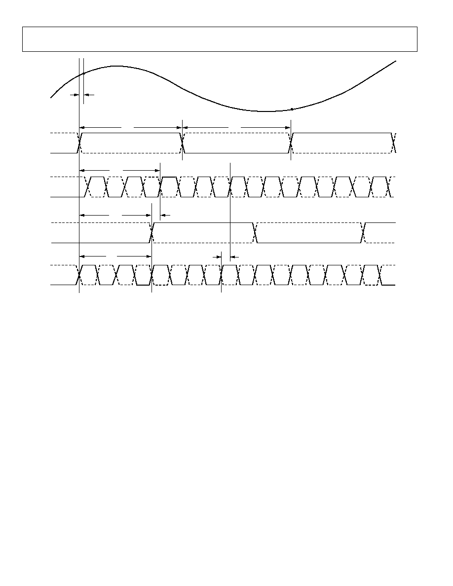
AD9222
Rev. 0 | Page 8 of 56
DCO
DCO+
D
D+
FCO
FCO+
AIN
CLK
CLK+
LSB
(N 8)
D0
(N 8)
D1
(N 8)
D2
(N 8)
D3
(N 8)
D4
(N 8)
D5
(N 8)
D6
(N 8)
D7
(N 8)
D8
(N 8)
D9
(N 8)
D10
(N 8)
D0
(N 7)
LSB
(N 7)
N 1
t
A
N
t
DATA
t
FRAME
t
FCO
t
PD
t
CPD
t
EH
t
EL
05
96
7-
00
4
Figure 4. 12-Bit Data Serial Stream, LSB First
AD9222
Rev. 0 | Page 9 of 56
ABSOLUTE MAXIMUM RATINGS
Table 5.
Parameter
With
Respect To
Rating
ELECTRICAL
AVDD
AGND
-0.3 V to +2.0 V
DRVDD
DRGND
-0.3 V to +2.0 V
AGND
DRGND
-0.3 V to +0.3 V
AVDD
DRVDD
-2.0 V to +2.0 V
Digital Outputs
(D+, D-, DCO+,
DCO-, FCO+, FCO-)
DRGND
-0.3 V to +2.0 V
CLK+, CLK-
AGND
-0.3 V to +3.9 V
VIN+, VIN-
AGND
-0.3 V to +2.0 V
SDIO/ODM
AGND
-0.3 V to +2.0 V
PDWN, SCLK/DTP, CSB
AGND
-0.3 V to +3.9 V
REFT, REFB, RBIAS
AGND
-0.3 V to +2.0 V
VREF, SENSE
AGND
-0.3 V to +2.0 V
ENVIRONMENTAL
Operating Temperature
Range (Ambient)
-40°C to +85°C
Maximum Junction
Temperature
150°C
Lead Temperature
(Soldering, 10 sec)
300°C
Storage Temperature
Range (Ambient)
-65°C to +150°C
Stresses above those listed under Absolute Maximum Ratings
may cause permanent damage to the device. This is a stress
rating only; functional operation of the device at these or any
other conditions above those indicated in the operational
section of this specification is not implied. Exposure to absolute
maximum rating conditions for extended periods may affect
device reliability.
THERMAL IMPEDANCE
Table 6.
Air Flow
Velocity (m/s)
JA
1
JB
JC
0.0 17.7°C/W
1.0 15.5°C/W
8.7°C/W
0.6°C/W
2.5 13.9°C/W
1
JA
for a 4-layer PCB with solid ground plane (simulated). Exposed pad
soldered to PCB.
ESD CAUTION
AD9222
Rev. 0 | Page 10 of 56
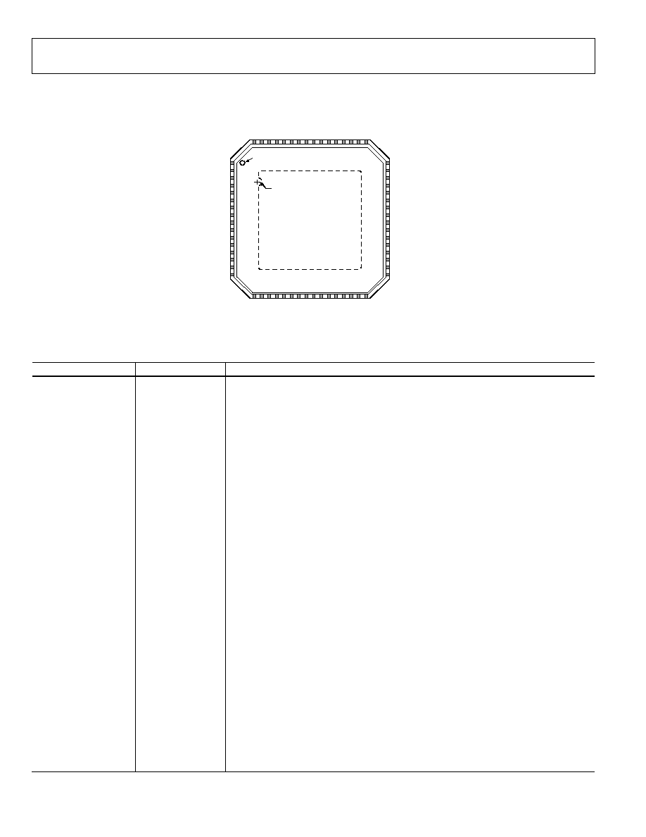
PIN CONFIGURATION AND FUNCTION DESCRIPTIONS
PIN 1
INDICATOR
17
18
19
20
21
22
23
24
25
26
27
28
29
30
31
32
DG
D+
G
DF
D+
F
DE
D+
E
DCO
DCO
+
FC
O
FC
O
+
DD
D+
D
DC
D+
C
DB
D+
B
64
63
62
61
60
59
58
57
56
55
54
53
52
51
50
49
VI
N
+
F
VI
N
F
AV
D
D
VI
N
E
VI
N
+
E
AV
D
D
RE
F
T
RE
F
B
VR
E
F
SEN
SE
RBI
AS
VI
N
+
D
VI
N
D
AV
D
D
VI
N
C
VI
N
+
C
1
2
3
4
5
6
7
8
9
10
11
12
13
14
15
16
AVDD
VIN+G
VING
AVDD
VINH
VIN+H
AVDD
AVDD
CLK
CLK+
AVDD
AVDD
DRGND
DRVDD
DH
D+H
NC = NO CONNECT
AVDD
VIN+B
VINB
AVDD
VINA
VIN+A
AVDD
PDWN
CSB
SDIO/ODM
SCLK/DTP
AVDD
DRGND
DRVDD
D+A
DA
48
47
46
45
44
43
42
41
40
39
38
37
36
35
34
33
AD9222
TOP VIEW
(Not to Scale)
05
96
7-
00
5
EXPOSED PADDLE, PIN 0
(BOTTOM OF PACKAGE)
Figure 5. 64-Lead LFCSP Top View
Table 7. Pin Function Descriptions
Pin No.
Mnemonic
Description
0
AGND
Analog Ground (Exposed Paddle)
1, 4, 7, 8, 11,
12, 37, 42, 45,
48, 51, 59, 62
AVDD
1.8 V Analog Supply
13, 36
DRGND
Digital Output Driver Ground
14, 35
DRVDD
1.8 V Digital Output Driver Supply
2
VIN+G
ADC G Analog Input--True
3
VIN-G
ADC G Analog Input--Complement
5
VIN-H
ADC H Analog Input--Complement
6
VIN+H
ADC H Analog Input--True
9
CLK-
Input Clock--Complement
10
CLK+
Input Clock--True
15
D-H
ADC H Digital Output--Complement
16
D+H
ADC H True Digital Output--True
17
D-G
ADC G Digital Output--Complement
18
D+G
ADC G True Digital Output--True
19
D-F
ADC F Digital Output--Complement
20
D+F
ADC F True Digital Output--True
21
D-E
ADC E Digital Output--Complement
22
D+E
ADC E True Digital Output--True
23
DCO-
Data Clock Digital Output--Complement
24
DCO+
Data Clock Digital Output--True
25
FCO-
Frame Clock Digital Output--Complement
26
FCO+
Frame Clock Digital Output--True
27
D-D
ADC D Digital Output--Complement
28
D+D
ADC D True Digital Output--True
29
D-C
ADC C Digital Output--Complement
30
D+C
ADC C True Digital Output
31
D-B
ADC B Digital Output--Complement
32
D+B
ADC B True Digital Output--True
33
D-A
ADC A Digital Output--Complement

AD9222
Rev. 0 | Page 11 of 56
Pin No.
Mnemonic
Description
34
D+A
ADC A True Digital Output--True
38
SCLK/DTP
Serial Clock/Digital Test Pattern
39
SDIO/ODM
Serial Data Input-Output/Output Driver Mode
40
CSB
Chip Select Bar
41 PDWN
Power
Down
43
VIN+A
ADC A Analog Input--True
44
VIN-A
ADC A Analog Input--Complement
46
VIN-B
ADC B Analog Input--Complement
47
VIN+B
ADC B Analog Input--True
49
VIN+C
ADC C Analog Input--True
50
VIN-C
ADC C Analog Input--Complement
52
VIN-D
ADC D Analog Input--Complement
53
VIN+D
ADC D Analog Input--True
54
RBIAS
External Resistor to Set the Internal ADC Core Bias Current
55
SENSE
Reference Mode Selection
56
VREF
Voltage Reference Input/Output
57
REFB
Differential Reference (Negative)
58
REFT
Differential Reference (Positive)
60
VIN+E
ADC E Analog Input--True
61
VIN-E
ADC E Analog Input--Complement
63
VIN-F
ADC F Analog Input--Complement
64
VIN+F
ADC F Analog Input--True
AD9222
Rev. 0 | Page 12 of 56
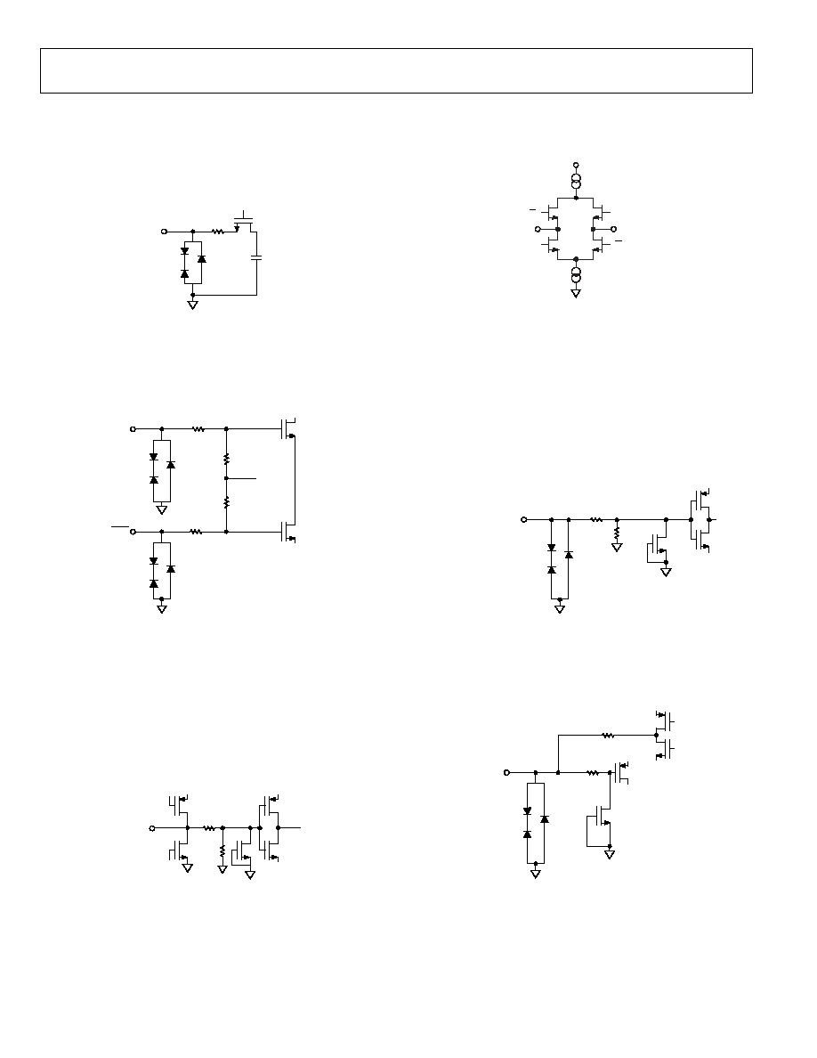
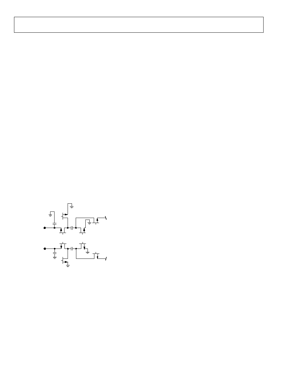
EQUIVALENT CIRCUITS
VIN
05
96
7-
0
06
Figure 6. Equivalent Analog Input Circuit
10
10k
10k
CLK
10
1.25V
CLK
059
67
-
0
07
Figure 7. Equivalent Clock Input Circuit
SDIO/ODM
350
30k
05
96
7
-
00
8
Figure 8. Equivalent SDIO/ODM Input Circuit
DRVDD
DRGND
D
D+
V
V
V
V
0
59
67
-
00
9
Figure 9. Equivalent Digital Output Circuit
SCLK/DTP OR PDWN
30k
1k
05
96
7-
01
0
Figure 10. Equivalent SCLK/DTP or PDWN Input Circuit
100
RBIAS
05
96
7-
0
11
Figure 11. Equivalent RBIAS Circuit
AD9222
Rev. 0 | Page 13 of 56
CSB
70k
1k
AVDD
05
96
7-
0
1
2
VREF
6k
0
59
67-
0
14
Figure 12. Equivalent CSB Input Circuit
Figure 14. Equivalent VREF Circuit
SENSE
1k
05
967
-
0
13
Figure 13. Equivalent SENSE Circuit
AD9222
Rev. 0 | Page 14 of 56
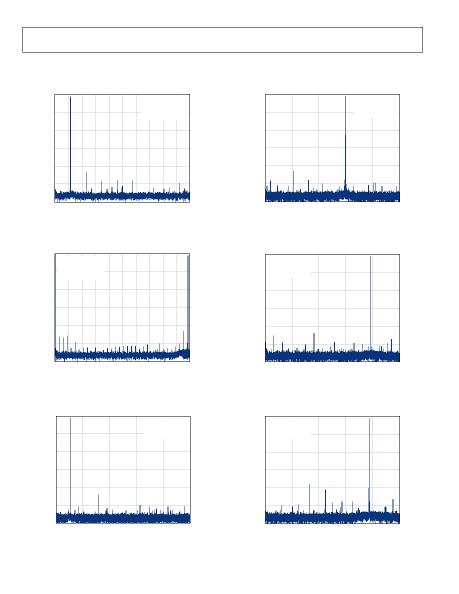
TYPICAL PERFORMANCE CHARACTERISTICS
0
596
7-
0
15
FREQUENCY (MHz)
A
M
PL
I
T
U
D
E (
d
B
F
S
)
120
0
0
20
100
80
60
40
20
2
4
6
8
10
12
14
16
18
AIN = 0.5dBFS
SNR = 70.79dB
ENOB = 11.47 BITS
SFDR = 84.71dBc
Figure 15. Single-Tone 32k FFT with f
IN
= 2.3 MHz, AD9222-40
05
96
7-
01
6
FREQUENCY (MHz)
A
M
PL
I
T
U
D
E (
d
B
F
S
)
120
0
0
20
0
120
100
80
60
40
20
0
5
10
15
20
25
AM
P
L
I
T
UDE
(
d
BF
S
)
FREQUENCY (MHz)
AIN = 0.5dBFS
SNR = 70.35dB
ENOB = 11.40 BITS
SFDR = 83.86dBc
05
96
7-
01
8
100
80
60
40
20
2
4
6
8
10
12
14
16
18
AIN = 0.5dBFS
SNR = 70.32dB
ENOB = 11.39 BITS
SFDR = 84.28dBc
Figure 16. Single-Tone 32k FFT with f
IN
= 19.7 MHz, AD9222-40
0
120
100
80
60
40
20
0
5
10
15
20
25
AM
P
L
I
T
UDE
(
d
BF
S
)
FREQUENCY (MHz)
AIN = 0.5dBFS
SNR = 70.72dB
ENOB = 11.45 BITS
SFDR = 85.79dBc
05
96
7-
01
7
Figure 17. Single-Tone 32k FFT with f
IN
= 2.3 MHz, AD9222-50
Figure 18. Single-Tone 32k FFT with f
IN
= 35 MHz, AD9222-50
0
120
100
80
60
40
20
0
5
10
15
20
25
AM
P
L
I
T
UDE
(
d
BF
S
)
FREQUENCY (MHz)
AIN = 0.5dBFS
SNR = 70.02dB
ENOB = 11.45 BITS
SFDR = 86.3dBc
05
96
7-
01
9
Figure 19. Single-Tone 32k FFT with f
IN
= 70 MHz, AD9222-50
0
120
100
80
60
40
20
0
5
10
15
20
25
AM
P
L
I
T
UDE
(
d
BF
S
)
FREQUENCY (MHz)
AIN = 0.5dBFS
SNR = 69.25dB
ENOB = 11.21 BITS
SFDR = 72.85dBc
05
96
7-
02
0
Figure 20. Single-Tone 32k FFT with f
IN
= 120 MHz, AD9222-50
AD9222
Rev. 0 | Page 15 of 56
100
90
95
85
80
75
70
65
60
10
50
45
40
35
30
25
20
15
S
N
R/
S
F
DR
(
d
B
)
ENCODE (MSPS)
2V p-p, SFDR
2V p-p, SNR
05
96
7-
02
1
Figure 21. SNR/SFDR vs. f
SAMPLE
, f
IN
= 2.61 MHz, AD9222-50
90
85
80
75
70
65
60
10
50
45
40
35
30
25
20
15
S
N
R/
S
F
DR
(
d
B
)
ENCODE (MSPS)
2V p-p, SFDR
2V p-p, SNR
05
96
7-
02
2
Figure 22. SNR/SFDR vs. f
SAMPLE
, f
IN
= 20.1 MHz, AD9222-50
100
90
80
70
60
50
40
30
20
10
0
60
50
40
30
20
10
0
S
N
R/
S
F
DR
(
d
B
)
INPUT AMPLITUDE (dBFS)
F
IN
= 10.3MHz
F
SAMPLE
= 50MSPS
80dB
REFERENCE
2V p-p, SFDR
2V p-p, SNR
05
96
7-
02
3
Figure 23. SNR/SFDR vs. Analog Input Level, f
IN
= 10.3 MHz, AD9222-50
100
90
80
70
60
50
40
30
20
10
0
60
50
40
30
20
10
0
S
N
R/
S
F
DR
(
d
B
)
INPUT AMPLITUDE (dBFS)
F
IN
= 35MHz
F
SAMPLE
= 50MSPS
80dB
REFERENCE
2V p-p, SFDR
2V p-p, SNR
05
96
7-
02
4
Figure 24. SNR/SFDR vs. Analog Input Level, f
IN
= 35 MHz, AD9222-50
0
120
100
80
60
40
20
0
2
4
6
8
10
12
14
16
18
20
AM
P
L
I
T
UDE
(
d
BF
S
)
FREQUENCY (MHz)
AIN1 AND AIN2 = 7dBFS
SFDR = 89.87dB
IMD2 = 96.07dBc
IMD3 = 90.16dBc
05
96
7-
02
5
Figure 25. Two-Tone 32k FFT with f
IN1
= 15 MHz and f
IN2
= 16 MHz,
AD9222-40
0
120
100
80
60
40
20
0
2
4
6
8
10
12
14
16
18
20
AM
P
L
I
T
UDE
(
d
BF
S
)
FREQUENCY (MHz)
AIN1 AND AIN2 = 7dBFS
SFDR = 77.24dB
IMD2 = 91.66dBc
IMD3 = 77.72dBc
05
96
7-
02
6
Figure 26. Two-Tone 32k FFT with f
IN1
= 70 MHz and f
IN2
= 71 MHz,
AD9222-40
AD9222
Rev. 0 | Page 16 of 56
0
120
100
80
60
40
20
0
5
10
15
20
25
AM
P
L
I
T
UDE
(
d
BF
S
)
FREQUENCY (MHz)
AIN1 AND AIN2 = 7dBFS
SFDR = 84.49dB
IMD2 = 85.83dBc
IMD3 = 84.54dBc
05
96
7-
02
7
Figure 27. Two-Tone 32k FFT with f
IN1
= 15 MHz and
f
IN2
= 16 MHz, AD9222-50
0
120
100
80
60
40
20
0
5
10
15
20
25
AM
P
L
I
T
UDE
(
d
BF
S
)
FREQUENCY (MHz)
AIN1 AND AIN2 = 7dBFS
SFDR = 80.42dB
IMD2 = 83.92dBc
IMD3 = 80.60dBc
05
96
7-
03
2
Figure 28. Two-Tone 32k FFT with f
IN1
= 70 MHz and
f
IN2
= 71 MHz, AD9222-50
90
85
80
75
70
65
60
1
1000
100
10
SN
R
/
S
F
D
R
(d
B
)
ANALOG INPUT FREQUENCY (MHz)
SFDR
SNR
05
96
7-
02
9
Figure 29. SNR/SFDR vs. f
IN
, AD9222-50
100
90
95
85
80
75
70
65
60
40
20
0
20
40
60
80
SI
N
A
D
/
SF
D
R
(d
B
)
TEMPERATURE (°C)
2V p-p, SFDR
2V p-p, SINAD
05
96
7-
03
0
Figure 30. SINAD/SFDR vs. Temperature, f
IN
= 2.61 MHz, AD9222-50
90
85
80
75
70
65
60
40
20
0
20
40
60
80
SI
N
A
D
/
SF
D
R
(d
B
)
TEMPERATURE (°C)
2V p-p, SFDR
2V p-p, SINAD
05
96
7-
03
1
Figure 31. SINAD/SFDR vs. Temperature, f
IN
= 20.1 MHz, AD9222-50
05
96
7-
03
6
CODE
IN
L
(
L
S
B
)
1.0
1.0
0
0.8
0.6
0.4
0.2
0
0.8
0.6
0.4
0.2
500
1000
1500
2000
2500
3000
3500
4000
Figure 32. INL, f
IN
= 2.3 MHz, AD9222-50
AD9222
Rev. 0 | Page 17 of 56
0.5
0.5
0.4
0.3
0.2
0.1
0
0.1
0.2
0.3
0.4
0
4000
3500
3000
2500
2000
1500
1000
500
DN
L
(
L
S
B
)
CODE
05
96
7-
03
3
Figure 33. DNL, f
IN
= 2.3 MHz, AD9222-50
05
96
7-
05
6
FREQUENCY (MHz)
CM
RR (
d
B
)
70
30
0
5
10
15
20
25
30
35
40
65
60
55
50
45
40
35
Figure 34. CMRR vs. Frequency, AD9222-50
1.8
1.6
1.4
1.2
1.0
0.8
0.6
0.4
0.2
0
N
N 1
N 2
N 3
N + 1
N + 2
N + 3
N
U
MB
E
R
OF
H
I
TS
(
M
illio
ns
)
CODE
0.27 LSB rms
05
96
7-
03
8
Figure 35. Input Referred Noise Histogram, AD9222-50
AM
P
L
I
T
UD
E
(
d
BF
S
)
120
0
20
40
60
80
100
0
5
10
15
20
25
FREQUENCY (MHz)
NPR = 60.3dB
NOTCH = 18.0MHz
NOTCH WIDTH = 3.0MHz
05
96
7-
0
41
Figure 36. Noise Power Ratio (NPR), AD9222-50
0
11
10
9
8
7
6
5
4
3
2
1
0
500
450
400
350
300
250
200
150
100
50
AM
P
L
I
T
UDE
(
d
BF
S
)
FREQUENCY (MHz)
3dB BANDWIDTH = 325MHz
05
96
7-
04
0
Figure 37. Full Power Bandwidth vs. Frequency, AD9222-50
AD9222
Rev. 0 | Page 18 of 56
THEORY OF OPERATION
The AD9222 architecture consists of a pipelined ADC that is
divided into three sections: a 4-bit first stage followed by eight
1.5-bit stages and a final 3-bit flash. Each stage provides
sufficient overlap to correct for flash errors in the preceding
stages. The quantized outputs from each stage are combined
into a final 12-bit result in the digital correction logic. The
pipelined architecture permits the first stage to operate on a
new input sample while the remaining stages operate on preceding
samples. Sampling occurs on the rising edge of the clock.
Each stage of the pipeline, excluding the last, consists of a low
resolution flash ADC connected to a switched-capacitor DAC
and interstage residue amplifier (MDAC). The residue amplifier
magnifies the difference between the reconstructed DAC output
and the flash input for the next stage in the pipeline. One bit of
redundancy is used in each stage to facilitate digital correction
of flash errors. The last stage simply consists of a flash ADC.
The output staging block aligns the data, carries out the error
correction, and passes the data to the output buffers. The data is
then serialized and aligned to the frame and output clock.
ANALOG INPUT CONSIDERATIONS
The analog input to the AD9222 is a differential switched-capacitor
circuit designed for processing differential input signals. The input
can support a wide common-mode range and maintain excellent
performance. An input common-mode voltage of midsupply
minimizes signal-dependent errors and provides optimum
performance.
S
S
H
C
PAR
C
SAMPLE
C
SAMPLE
C
PAR
VIN
H
S
S
H
VIN+
H
0
59
67
-
04
3
Figure 38. Switched-Capacitor Input Circuit
The clock signal alternately switches the input circuit between
sample mode and hold mode (see Figure 38). When the input
circuit is switched into sample mode, the signal source must be
capable of charging the sample capacitors and settling within
one-half of a clock cycle. A small resistor in series with each
input can help reduce the peak transient current injected from
the output stage of the driving source. In addition, low-Q inductors
or ferrite beads can be placed on each leg of the input to reduce
the high differential capacitance seen at the analog inputs, thus
realizing the maximum bandwidth of the ADC. Such use of
low-Q inductors or ferrite beads is required when driving the
converter front end at high IF frequencies. Either a shunt capacitor
or two single-ended capacitors can be placed on the inputs to
provide a matching passive network. This ultimately creates a
low-pass filter at the input to limit any unwanted broadband
noise. See the AN-742 Application Note, the AN-827 Application
Note, and the Analog Dialogue article "Transformer-Coupled
Front-End for Wideband A/D Converters" for more information
on this subject. In general, the precise values depend on the
application.
The analog inputs of the AD9222 are not internally dc-biased.
In ac-coupled applications, the user must provide this bias
externally. Setting the device so that V
CM
= AVDD/2 is recom-
mended for optimum performance, but the device can function
over a wider range with reasonable performance, as shown in
Figure 39 and Figure 40.
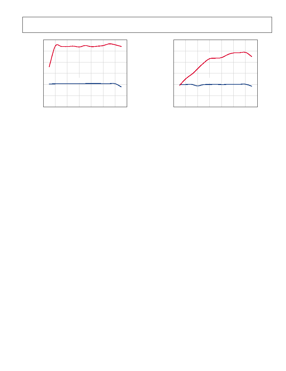
AD9222
Rev. 0 | Page 19 of 56
90
85
80
75
70
65
60
0.2
1.6
1.4
1.2
1.0
0.8
0.6
0.4
S
N
R/
S
F
DR
(
d
B
)
ANALOG INPUT COMMON-MODE VOLTAGE (V)
SFDR (dBc)
SNR (dB)
05
96
7-
04
4
Figure 39. SNR/SFDR vs. Common-Mode Voltage,
f
IN
= 2.3 MHz, AD9222-50
90
85
80
75
70
65
60
0.2
1.6
1.4
1.2
1.0
0.8
0.6
0.4
S
N
R/
S
F
DR
(
d
B
)
ANALOG INPUT COMMON-MODE VOLTAGE (V)
SFDR (dBc)
SNR (dB)
05
96
7-
04
2
Figure 40. SNR/SFDR vs. Common-Mode Voltage,
f
IN
= 35 MHz, AD9222-50
AD9222
Rev. 0 | Page 20 of 56
For best dynamic performance, the source impedances driving
VIN+ and VIN- should be matched such that common-mode
settling errors are symmetrical. These errors are reduced by the
common-mode rejection of the ADC. An internal reference
buffer creates the positive and negative reference voltages, REFT
and REFB, respectively, that define the span of the ADC core.
The output common-mode of the reference buffer is set to
midsupply, and the REFT and REFB voltages and span are
defined as
REFT = 1/2 (AVDD + VREF)
REFB = 1/2 (AVDD - VREF)
Span = 2 × (REFT - REFB) = 2 × VREF
It can be seen from these equations that the REFT and REFB
voltages are symmetrical about the midsupply voltage and, by
definition, the input span is twice the value of the VREF voltage.
Maximum SNR performance is always achieved by setting the
ADC to the largest span in a differential configuration. In the
case of the AD9222, the largest input span available is 2 V p-p.
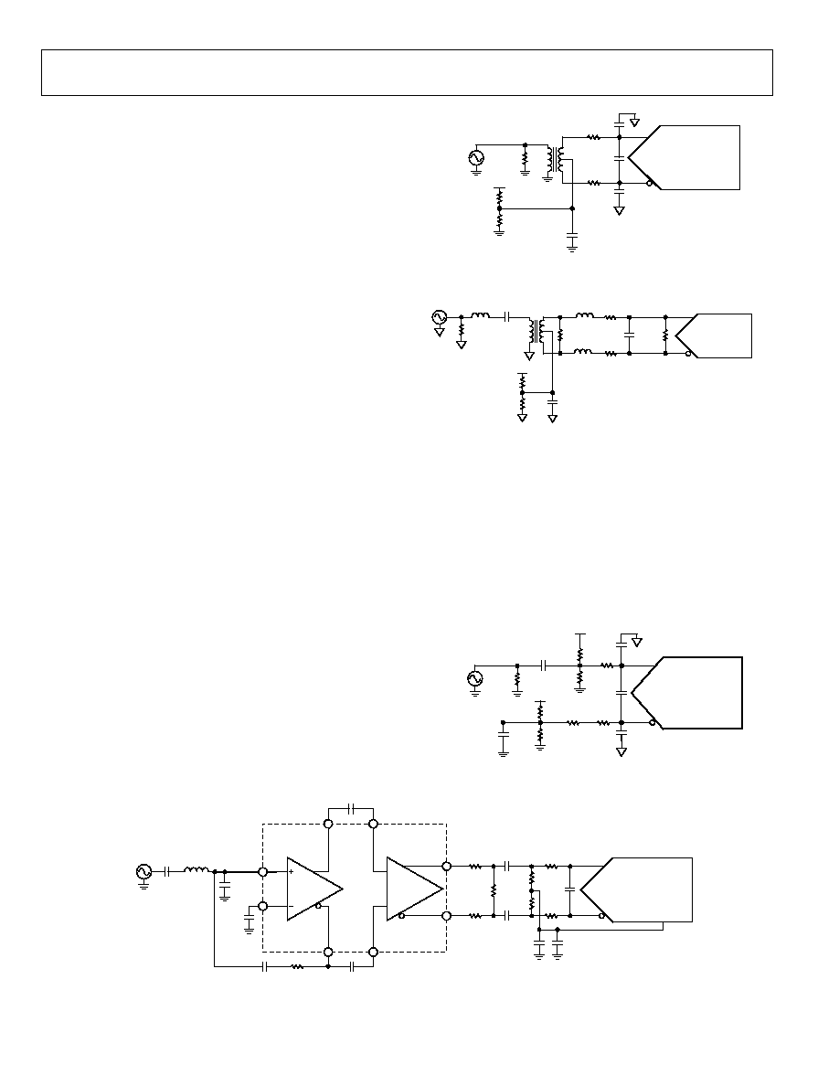
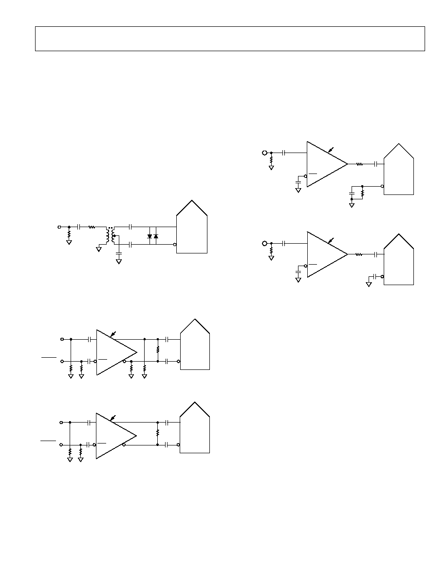
Differential Input Configurations
There are several ways in which to drive the AD9222 either
actively or passively. In either case, the optimum performance is
achieved by driving the analog input differentially. One example
is by using the AD8334 differential driver. It provides excellent
performance and a flexible interface to the ADC (see Figure 44)
for baseband applications. This configuration is common for
medical ultrasound systems.
However, the noise performance of most amplifiers is not
adequate to achieve the true performance of the AD9222. For
applications where SNR is a key parameter, differential transfor-
mer coupling is the recommended input configuration. Two
examples are shown in Figure 41 and Figure 42.
In any configuration, the value of the shunt capacitor, C, is
dependent on the input frequency and may need to be reduced
or removed.
2V p-p
R
R
1
C
DIFF
C
1
C
DIFF
IS OPTIONAL.
49.9
0.1F
1k
1k
AGND
AVDD
ADT11WT
1:1 Z RATIO
VIN
ADC
AD9222
VIN+
C
05
96
7-
04
6
Figure 41. Differential Transformer-Coupled Configuration
for Baseband Applications
ADC
AD9222
2V p-p
2.2pF
1k
0.1F
1k
1k
AVDD
ADT11WT
1:1 Z RATIO
16nH
16nH
0.1F
16nH
33
33
499
65
VIN+
VIN
059
67
-
04
7
Figure 42. Differential Transformer-Coupled Configuration for IF Applications
Single-Ended Input Configuration
A single-ended input may provide adequate performance in
cost-sensitive applications. In this configuration, SFDR and
distortion performance degrade due to the large input common-
mode swing. If the application requires a single-ended input
configuration, ensure that the source impedances on each input
are well matched in order to achieve the best possible performance.
A full-scale input of 2 V p-p can still be applied to the ADC's VIN+
pin while the VIN- pin is terminated. Figure 43 details a typical
single-ended input configuration.
2V p-p
R
R
49.9
0.1µF
0.1µF
AVDD
1k 25
1k
1k
AVDD
VIN
ADC
AD9222
VIN+
1
C
DIFF
C
1
C
DIFF
IS OPTIONAL.
C
05
967
-
04
8
Figure 43. Single-Ended Input Configuration
AD8334
1.0k
1.0k
374
187
R
R
C
0.1F
187
0.1F
0.1F
0.1F
0.1F
10F
0.1F
1V p-p
0.1F
LNA
120nH
VGA
VOH
VIP
INH
22pF
LMD
VIN
LOP
LON
VOL
18nF
274
VIN
ADC
AD9222
VIN+
VREF
05
96
7-
0
49
Figure 44. Differential Input Configuration Using the AD8334
AD9222
Rev. 0 | Page 21 of 56
CLOCK INPUT CONSIDERATIONS
For optimum performance, the AD9222 sample clock inputs
(CLK+ and CLK-) should be clocked with a differential signal.
This signal is typically ac-coupled into the CLK+ and CLK- pins
via a transformer or capacitors. These pins are biased internally
and require no additional bias.
Figure 45 shows one preferred method for clocking the AD9222.
The low jitter clock source is converted from single-ended to
differential using an RF transformer. The back-to-back Schottky
diodes across the secondary transformer limit clock excursions
into the AD9222 to approximately 0.8 V p-p differential. This
helps prevent the large voltage swings of the clock from feeding
through to other portions of the AD9222 and preserves the fast
rise and fall times of the signal, which are critical to low jitter
performance.
0.1µF
0.1µF
0.1µF
0.1µF
SCHOTTKY
DIODES:
HSM2812
CLOCK
INPUT
50
100
CLK
CLK+
ADC
AD9222
MIN-CIRCUITS
ADT11WT, 1:1Z
XFMR
05
96
7-
05
0
Figure 45. Transformer-Coupled Differential Clock
If a low jitter clock is available, another option is to ac-couple a
differential PECL signal to the sample clock input pins as shown
in Figure 46. The AD9510/AD9511/AD9512/AD9513/AD9514/
AD9515 family of clock drivers offers excellent jitter performance.
CLOCK
INPUT
100
0.1µF
0.1µF
0.1µF
0.1µF
240
240
CLOCK
INPUT
AD9510/AD9511/
AD9512/AD9513/
AD9514/AD9515
50
1
50
1
CLK
CLK
1
50
RESISTORS ARE OPTIONAL.
CLK
CLK+
ADC
AD9222
05
967-
051
PECL DRIVER
Figure 46. Differential PECL Sample Clock
CLOCK
INPUT
100
0.1µF
0.1µF
0.1µF
0.1µF
50
1
CLOCK
INPUT
LVDS DRIVER
50
1
CLK
CLK
1
50 RESISTORS ARE OPTIONAL.
CLK
CLK+
ADC
AD9222
059
67-
05
2
AD9510/AD9511/
AD9512/AD9513/
AD9514/AD9515
Figure 47. Differential LVDS Sample Clock
In some applications, it is acceptable to drive the sample clock
inputs with a single-ended CMOS signal. In such applications,
CLK+ should be directly driven from a CMOS gate, and the
CLK- pin should be bypassed to ground with a 0.1 F capacitor
in parallel with a 39 k resistor (see Figure 48). Although the
CLK+ input circuit supply is AVDD (1.8 V), this input is
designed to withstand input voltages up to 3.3 V, making the
selection of the drive logic voltage very flexible.
CLOCK
INPUT
0.1µF
0.1µF
0.1µF
39
k
CMOS DRIVER
50
1
OPTIONAL
100
0.1µF
CLK
CLK
1
50 RESISTOR IS OPTIONAL.
CLK
CLK+
ADC
AD9222
0596
7-
053
AD9510/AD9511/
AD9512/AD9513/
AD9514/AD9515
Figure 48. Single-Ended 1.8 V CMOS Sample Clock
CLOCK
INPUT
0.1µF
0.1µF
0.1µF
CMOS DRIVER
50
1
OPTIONAL
100
CLK
CLK
1
50
RESISTOR IS OPTIONAL.
0.1µF
CLK
CLK+
ADC
AD9222
0596
7-
05
4
AD9510/AD9511/
AD9512/AD9513/
AD9514/AD9515
Figure 49. Single-Ended 3.3 V CMOS Sample Clock
Clock Duty Cycle Considerations
Typical high speed ADCs use both clock edges to generate a
variety of internal timing signals. As a result, these ADCs may
be sensitive to clock duty cycle. Commonly, a 5% tolerance is
required on the clock duty cycle to maintain dynamic performance
characteristics. The AD9222 contains a duty cycle stabilizer (DCS)
that retimes the nonsampling edge, providing an internal clock
signal with a nominal 50% duty cycle. This allows a wide range
of clock input duty cycles without affecting the performance of
the AD9222. When the DCS is on, noise and distortion perfor-
mance are nearly flat for a wide range of duty cycles. However,
some applications may require the DCS function to be off. If so,
keep in mind that the dynamic range performance can be affected
when operated in this mode. See the Memory Map section for
more details on using this feature.
The duty cycle stabilizer uses a delay-locked loop (DLL) to
create the nonsampling edge. As a result, any changes to the
sampling frequency require approximately eight clock cycles
to allow the DLL to acquire and lock to the new rate.
AD9222
Rev. 0 | Page 22 of 56
Clock Jitter Considerations
High speed, high resolution ADCs are sensitive to the quality of the
clock input. The degradation in SNR at a given input frequency
(f
A
) due only to aperture jitter (t
J
) can be calculated by
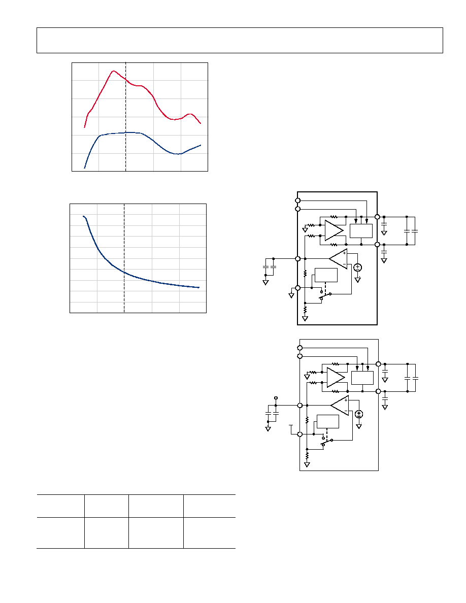
SNR degradation = 20 × log 10 [1/2 × × f
A
× t
J
]
In this equation, the rms aperture jitter represents the root mean
square of all jitter sources, including the clock input, analog input
signal, and ADC aperture jitter specifications. IF undersampling
applications are particularly sensitive to jitter (see Figure 50).
The clock input should be treated as an analog signal in cases
where aperture jitter may affect the dynamic range of the AD9222.
Power supplies for clock drivers should be separated from the
ADC output driver supplies to avoid modulating the clock signal
with digital noise. Low jitter, crystal-controlled oscillators make
the best clock sources. If the clock is generated from another
type of source (by gating, dividing, or other methods), it should
be retimed by the original clock at the last step.
Refer to the AN-501 Application Note
and the AN-756
Application Note for more in-depth information about jitter
performance as it relates to ADCs (visit
www.analog.com
).
1
10
100
1000
16 BITS
14 BITS
12 BITS
30
40
50
60
70
80
90
100
110
120
130
0.125ps
0.25ps
0.5ps
1.0ps
2.0ps
ANALOG INPUT FREQUENCY (MHz)
10 BITS
8 BITS
RMS CLOCK JITTER REQUIREMENT
S
NR (
d
B
)
059
66
-
03
8
Figure 50. Ideal SNR vs. Input Frequency and Jitter
Power Dissipation and Power-Down Mode
As shown in Figure 51, the power dissipated by the AD9222 is
proportional to its sample rate. The digital power dissipation
does not vary much because it is determined primarily by the
DRVDD supply and bias current of the LVDS output drivers.
05
967
-
05
7
ENCODE (MSPS)
C
URR
E
NT
(
A
)
10
50
0
0.05
0.10
0.15
0.20
0.25
0.30
0.35
0.40
15
20
25
30
35
40
45
0.500
0.550
0.600
0.650
0.700
0.750
0.800
PO
WER
(
W
)
TOTAL POWER
AVDD CURRENT
DRVDD CURRENT
Figure 51. Supply Current vs. f
SAMPLE
for f
IN
= 10.3 MHz, AD9222- 50
AD9222
Rev. 0 | Page 23 of 56
By asserting the PDWN pin high, the AD9222 is placed in
power-down mode. In this state, the ADC typically dissipates
11 mW. During power-down, the LVDS output drivers are placed
in a high impedance state. The AD9222 returns to normal
operating mode when the PDWN pin is pulled low. This pin is
both 1.8 V and 3.3 V tolerant.
In power-down mode, low power dissipation is achieved by
shutting down the reference, reference buffer, PLL, and biasing
networks. The decoupling capacitors on REFT and REFB are
discharged when entering power-down mode and must be
recharged when returning to normal operation. As a result, the
wake-up time is related to the time spent in the power-down
mode; shorter cycles result in proportionally shorter wake-up
times. With the recommended 0.1 F and 4.7 F decoupling
capacitors on REFT and REFB, it takes approximately 1 sec to
fully discharge the reference buffer decoupling capacitors and
375 s to restore full operation.
There are a number of other power-down options available
when using the SPI port interface. The user can individually
power down each channel or put the entire device into standby
mode. This allows the user to keep the internal PLL powered
when fast wake-up times (~600 ns) are required. See the
Memory Map section for more details on using these features.
Digital Outputs and Timing
The AD9222 differential outputs conform to the ANSI-644 LVDS
standard on default power-up. This can be changed to a low power,
reduced signal option similar to the IEEE 1596.3 standard using the
SDIO/ODM pin or via the SPI. This LVDS standard can further
reduce the overall power dissipation of the device by approximately
36 mW. See the SDIO/ODM Pin section or Table 15 in the
Memory Map section for more information. The LVDS driver
current is derived on-chip and sets the output current at each
output equal to a nominal 3.5 mA. A 100 differential termination
resistor placed at the LVDS receiver inputs results in a nominal
350 mV swing at the receiver.
The AD9222 LVDS outputs facilitate interfacing with LVDS
receivers in custom ASICs and FPGAs that have LVDS capability
for superior switching performance in noisy environments.
Single point-to-point net topologies are recommended with a
100 termination resistor placed as close to the receiver as
possible. No far-end receiver termination and poor differential
trace routing may result in timing errors. It is recommended
that the trace length is no longer than 24 inches and that the
differential output traces are kept close together and at equal
lengths. An example of the FCO and data stream with proper
trace length and position can be found in Figure 52.
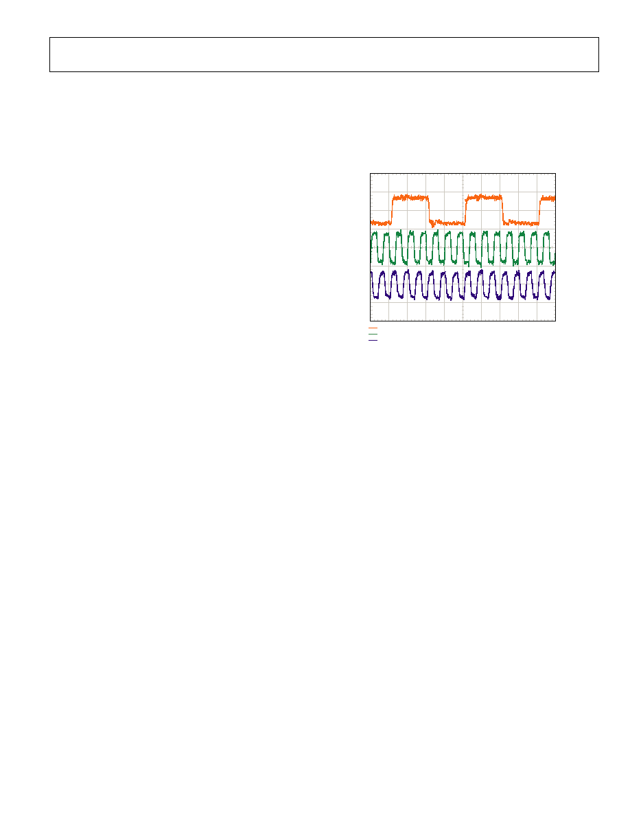
CH1 500mV/DIV = FCO
CH2 500mV/DIV = DCO
CH3 500mV/DIV = DATA
5.0ns/DIV
0
596
7-
0
58
Figure 52. LVDS Output Timing Example in ANSI Mode (Default), AD9222-50
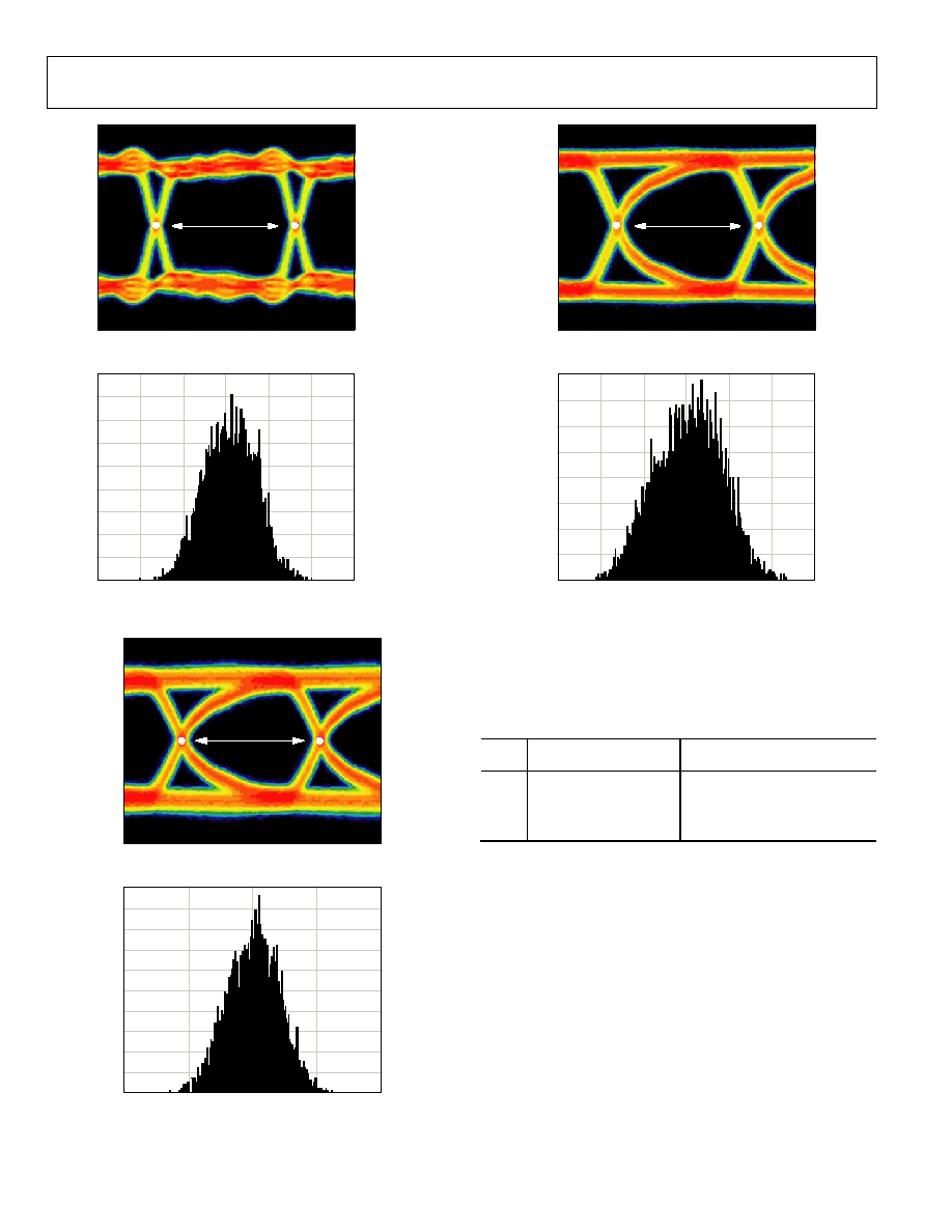
An example of the LVDS output using the ANSI standard (default)
data eye and a time interval error (TIE) jitter histogram with
trace lengths less than 24 inches on regular FR-4 material is
shown in Figure 53. Figure 54 shows an example of when the
trace lengths exceed 24 inches on regular FR-4 material. Notice
that the TIE jitter histogram reflects the decrease of the data eye
opening as the edge deviates from the ideal position. It is up to
the user to determine if the waveforms meet the timing budget
of the design when the trace lengths exceed 24 inches. Additional
SPI options allow the user to further increase the internal ter-
mination (increasing the current) of all eight outputs in order to
drive longer trace lengths (see Figure 55). Even though this
produces sharper rise and fall times on the data edges and is less
prone to bit errors, the power dissipation of the DRVDD supply
increases when this option is used. Also notice in Figure 55 that
the histogram has improved.
In cases that require increased driver strength to the DCO and
FCO outputs because of load mismatch, Register 15 allows the
user to increase the drive strength by 2×. To do this, set the
appropriate bit in Register 5. Note that this feature cannot be
used with Bit 4 and Bit 5 in Register 15. Bit 4 and Bit 5 will take
precedence over this feature. See the Memory Map section for
more details.
AD9222
Rev. 0 | Page 24 of 56
500
400
300
200
100
500
400
300
200
100
0
1.0ns
1.5ns
0.5ns
0ns
0.5ns
1.0ns
1.5ns
EY
E D
I
A
G
R
A
M V
O
L
T
A
G
E (
m
V)
EYE: ALL BITS
ULS: 12071/12071
90
50
10
20
30
40
60
70
80
0
150ps
100ps
50ps
0ps
50ps
100ps
150ps
T
I
E
J
I
T
T
ER H
I
ST
O
G
R
AM
(Hi
t
s
)
0
596
7-
06
1
Figure 53. Data Eye for LVDS Outputs in ANSI Mode with Trace Lengths Less
than 24 Inches on Standard FR-4, AD9222-50
60
80
90
70
50
40
20
10
100
30
0
200ps
100ps
100ps
0ps
200ps
T
I
E J
I
T
T
ER
HI
S
T
O
G
R
AM (
H
i
t
s
)
500
400
300
200
100
500
400
300
200
100
0
1.0ns
0.5ns
0ns
0.5ns
1.5ns
1.5ns
1.0ns
E
Y
E
DI
AG
RAM
V
O
L
T
A
G
E
(
m
V
)
EYE: ALL BITS
ULS: 12067/12067
0
5
967
-
05
9
Figure 54. Data Eye for LVDS Outputs in ANSI Mode with Trace Lengths
Greater than 24 Inches on Standard FR-4, AD9222-50
400
300
200
100
400
300
200
100
0
0.5ns
0ns
0.5ns
EY
E D
I
A
G
R
A
M V
O
L
T
A
G
E
(
m
V)
EYE: ALL BITS
ULS: 12072/12072
80
50
10
20
30
40
60
70
0
150ps
100ps
50ps
0ps
50ps
100ps
150ps
T
I
E
J
I
T
T
E
R H
I
ST
O
G
R
AM
(Hi
t
s
)
1.0ns
1.5ns
1.5ns
1.0ns
0
596
7-
06
0
Figure 55. Data Eye for LVDS Outputs in ANSI Mode with 100 Termination
on and Trace Lengths Greater than 24 Inches on Standard FR-4, AD9222-50
The format of the output data is offset binary by default. An
example of the output coding format can be found in Table 8.
If it is desired to change the output data format to twos
complement, see the Memory Map section.
Table 8. Digital Output Coding
Code
(VIN+) - (VIN-), Input
Span = 2 V p-p (V)
Digital Output Offset Binary
(D11 ... D0)
4095
+1.00
1111 1111 1111
2048
0.00
1000 0000 0000
2047
-0.000488
0111 1111 1111
0
-1.00
0000 0000 0000
Data from each ADC is serialized and provided on a separate
channel. The data rate for each serial stream is equal to 12 bits
times the sample clock rate, with a maximum of 600 Mbps
(12 bits × 50 MSPS = 600 Mbps). The lowest typical conversion
rate is 10 MSPS. However, if lower sample rates are required for
a specific application, the PLL can be set up for encode rates
lower than 10 MSPS via the SPI. This allows encode rates as low
as 5 MSPS. See the Memory Map section to enable this feature.

AD9222
Rev. 0 | Page 25 of 56
Two output clocks are provided to assist in capturing data from
the AD9222. The DCO is used to clock the output data and is
equal to six times the sampling clock (CLK) rate. Data is
clocked out of the AD9222 and must be captured on the rising
and falling edges of the DCO that supports double data rate
(DDR) capturing. The frame clock out (FCO) is used to signal
the start of a new output byte and is equal to the sampling clock
rate. See the timing diagram shown in Figure 2 for more
information.
Table 9. Flex Output Test Modes
Output Test
Mode Bit
Sequence
Pattern Name
Digital Output Word 1
Digital Output Word 2
Subject
to Data
Format
Select
0000 Off
(default)
N/A
N/A
N/A
0001 Midscale
short 1000 0000 (8-bit)
10 0000 0000 (10-bit)
1000 0000 0000 (12-bit)
10 0000 0000 0000 (14-bit)
Same Yes
0010 +Full-scale
short 1111 1111 (8-bit)
11 1111 1111 (10-bit)
1111 1111 1111 (12-bit)
11 1111 1111 1111 (14-bit)
Same Yes
0011 -Full-scale
short 0000 0000 (8-bit)
00 0000 0000 (10-bit)
0000 0000 0000 (12-bit)
00 0000 0000 0000 (14-bit)
Same Yes
0100 Checker
board 1010 1010 (8-bit)
10 1010 1010 (10-bit)
1010 1010 1010 (12-bit)
10 1010 1010 1010 (14-bit)
0101 0101 (8-bit)
01 0101 0101 (10-bit)
0101 0101 0101 (12-bit)
01 0101 0101 0101 (14-bit)
No
0101
PN sequence long
1
N/A N/A Yes
0110
PN sequence short
1
N/A
N/A
Yes
0111 One/zero
word
toggle
1111 1111 (8-bit)
11 1111 1111 (10-bit)
1111 1111 1111 (12-bit)
11 1111 1111 1111 (14-bit)
0000 0000 (8-bit)
00 0000 0000 (10-bit)
0000 0000 0000 (12-bit)
00 0000 0000 0000 (14-bit)
No
1000
User input
Register 0x19 to Register 0x1A
Register 0x1B to Register 0x1C
No
1001
One/zero bit toggle
1010 1010 (8-bit)
10 1010 1010 (10-bit)
1010 1010 1010 (12-bit)
10 1010 1010 1010 (14-bit)
N/A No
1010 1×
sync
0000 1111 (8-bit)
00 0001 1111 (10-bit)
0000 0011 1111 (12-bit)
00 0000 0111 1111 (14-bit)
N/A No
1011
One bit high
1000 0000 (8-bit)
10 0000 0000 (10-bit)
1000 0000 0000 (12-bit)
10 0000 0000 0000 (14-bit)
N/A No
1100 Mixed
frequency 1010 0011 (8-bit)
10 0110 0011 (10-bit)
1010 0011 0011 (12-bit)
10 1000 0110 0111 (14-bit)
N/A No
1
PN, or pseudorandom number, sequence is determined by the number of bits in the shift register. The long sequence is 23 bits and the short sequence is
9 bits. How the sequence is generated and utilized is described in the ITU O.150 standard. In general, the polynomial, X23 + X18 + 1 (long) and X9 + X5 + 1
(short), defines the pseudorandom sequence.
AD9222
Rev. 0 | Page 26 of 56
When using the serial port interface (SPI), the DCO phase can
be adjusted in 60° increments relative to the data edge. This
enables the user to refine system timing margins if required.
The default DCO timing, as shown in Figure 2, is 90° relative to
the output data edge.
An 8-, 10-, and 14-bit serial stream can also be initiated from
the SPI. This allows the user to implement and test compatibility
to lower and higher resolution systems. When changing the
resolution to an 8- or 10-bit serial stream, the data stream is
shortened. See Figure 3 for the 10-bit example. However, when
using the 14-bit option, the data stream stuffs two 0s at the end
of the normal 14-bit serial data.
When using the SPI, all of the data outputs can also be inverted
from their nominal state. This is not to be confused with
inverting the serial stream to an LSB-first mode. In default
mode, as shown in Figure 2, the MSB is represented first in the
data output serial stream. However, this can be inverted so that
the LSB is represented first in the data output serial stream (see
Figure 4).
There are 12 digital output test pattern options available that
can be initiated through the SPI. This is a useful feature when
validating receiver capture and timing. Refer to Table 9 for the
output bit sequencing options available. Some test patterns have
two serial sequential words and can be alternated in various
ways, depending on the test pattern chosen. It should be noted
that some patterns may not adhere to the data format select
option. In addition, customer user patterns can be assigned in
the 0x19, 0x1A, 0x1B, and 0x1C register addresses. All test mode
options can support 8- to 14-bit word lengths in order to verify
data capture to the receiver.
Please consult the Memory Map section for information on how
to change these additional digital output timing features through
the serial port interface or SPI.
SDIO/ODM Pin
This pin is for applications that do not require SPI mode operation.
The SDIO/ODM pin can enable a low power, reduced signal option
similar to the IEEE 1596.3 reduced range link output standard if
this pin and the CSB pin are tied to AVDD during device power-
up. This option should only be used when the digital output trace
lengths are less than 2 inches from the LVDS receiver. The FCO,
DCO, and outputs function normally, but the LVDS signal swing
of all channels is reduced from 350 mV p-p to 200 mV p-p. This
output mode allows the user to further lower the power on the
DRVDD supply. For applications where this pin is not used, it
should be tied low. In this case, the device pin can be left open,
and the 30 k internal pull-down resistor pulls this pin low. This
pin is only 1.8 V tolerant. If applications require this pin to be
driven from a 3.3 V logic level, insert a 1 k resistor in series
with this pin to limit the current.
Table 10. Output Driver Mode Pin Settings
Selected ODM
ODM Voltage
Resulting
Output Standard
Resulting
FCO and DCO
Normal
operation
10 k to AGND
ANSI-644
(default)
ANSI-644
(default)
ODM AVDD
Low power,
reduced signal
option
Low power,
reduced
signal
option
SCLK/DTP Pin
This pin is for applications that do not require SPI mode operation.
The serial clock/digital test pattern (SCLK/DTP) pin can enable
a single digital test pattern if this pin and the CSB pin are held
high during device power-up. When the DTP is tied to AVDD,
all the ADC channel outputs shift out the following pattern:
1000 0000 0000. The FCO and DCO outputs still work as usual
while all channels shift out the repeatable test pattern. This pattern
allows the user to perform timing alignment adjustments among
the FCO, DCO, and output data. For normal operation, this pin
should be tied to AGND through a 10 k resistor. This pin is
both 1.8 V and 3.3 V tolerant.
Table 11. Digital Test Pattern Pin Settings
Selected DTP
DTP Voltage
Resulting
D+ and D-
Resulting
FCO and DCO
Normal
operation
10 k to AGND
Normal
operation
Normal operation
DTP
AVDD
1000 0000 0000
Normal operation
Additional and custom test patterns can also be observed when
commanded from the SPI port. Consult the Memory Map
section to choose from the different options available.
CSB Pin
The chip select bar (CSB) pin should be tied to AVDD for
applications that do not require SPI mode operation. By tying
CSB high, all SCLK and SDIO information is ignored. This pin
is both 1.8 V and 3.3 V tolerant.
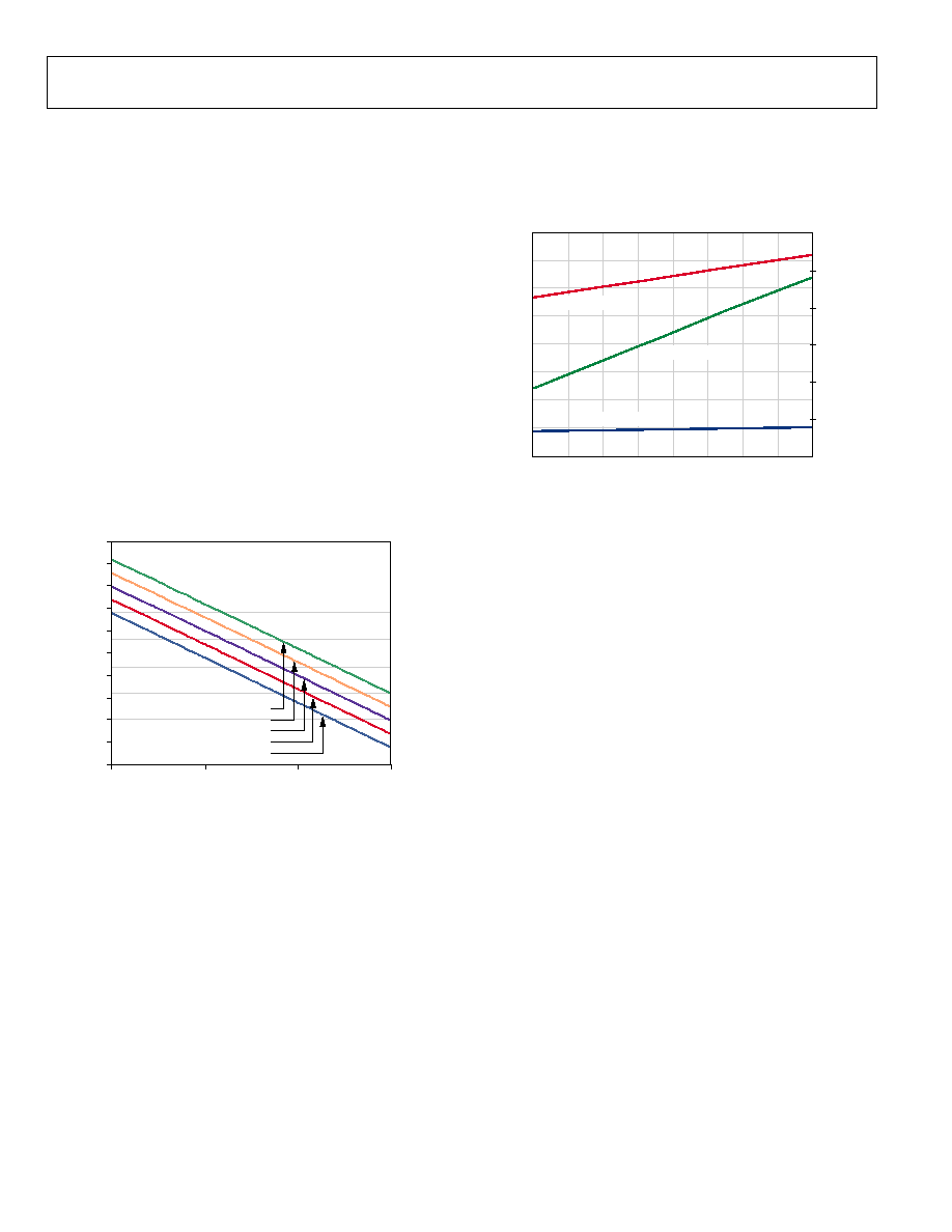
RBIAS Pin
To set the internal core bias current of the ADC, place a resistor
(nominally equal to 10.0 k) to ground at the RBIAS pin. The
resistor current is derived on-chip and sets the ADC's AVDD
current to a nominal 358 mA at 50 MSPS. Therefore, it is
imperative that at least a 1% tolerance on this resistor be used to
achieve consistent performance. If SFDR performance is not as
critical as power, simply adjust the ADC core current to achieve
a lower power. Figure 56 and Figure 57 show the relationship
between the dynamic range and power as the RBIAS resistance
is changed. Nominally, a 10.0 k value is used, as indicated by
the dashed line.
AD9222
Rev. 0 | Page 27 of 56
90
85
80
75
70
65
60
0
5
10
15
20
25
S
N
R/
S
F
DR
(
d
B
)
R
BIAS
(k)
05
96
7-
06
2
SNR
SFDR
Figure 56. SNR/SFDR vs. RBIAS, F
IN
= 10.3 MHz, AD9222-50
059
67
-
0
63
R
BIAS
(k)
IA
V
D
D
(
A
)
0
0.1
0.2
0.3
0.4
0.5
0.6
0.7
0.8
0.9
1.0
0
5
10
15
20
25
Figure 57. IAVDD vs. RBIAS, AD9222-50
Voltage Reference
A stable and accurate 0.5 V voltage reference is built into the
AD9222. This is gained up by a factor of 2 internally, setting
V
REF
to 1.0 V, which results in a full-scale differential input span
of 2 V p-p. The V
REF
is set internally by default; however, the
VREF pin can be driven externally with a 1.0 V reference to
achieve more accuracy.
When applying the decoupling capacitors to the VREF, REFT,
and REFB pins, use ceramic low ESR capacitors. These capacitors
should be close to the ADC pins and on the same layer of the
PCB as the AD9222. The recommended capacitor values and
configurations for the AD9222 reference pin can be found in
Figure 58.
Table 12. Reference Settings
Selected
Mode
SENSE
Voltage
Resulting
VREF (V)
Resulting
Differential
Span (V p-p)
External
Reference
AVDD
N/A
2 × external
reference
Internal,
2 V p-p FSR
AGND to 0.2 V
1.0
2.0
Internal Reference Operation
A comparator within the AD9222 detects the potential at the
SENSE pin and configures the reference. If SENSE is grounded,
the reference amplifier switch is connected to the internal
resistor divider (see Figure 58), setting VREF to 1 V.
The REFT and REFB pins establish their input span of the ADC
core from the reference configuration. The analog input full-
scale range of the ADC equals twice the voltage at the reference
pin for either an internal or an external reference configuration.
If the reference of the AD9222 is used to drive multiple
converters to improve gain matching, the loading of the refer-
ence by the other converters must be considered. Figure 60
depicts how the internal reference voltage is affected by loading.
1µF
0.1µF
V
REF
SENSE
0.5V
REFT
0.1µF
0.1µF
2.2µF
0.1µF
REFB
SELECT
LOGIC
ADC
CORE
+
VIN
VIN+
05
96
7-
0
64
Figure 58. Internal Reference Configuration
1µF
1
0.1µF
1
V
REF
SENSE
AVDD
0.5V
REFT
0.1µF
0.1µF
2.2µF
0.1µF
REFB
SELECT
LOGIC
ADC
CORE
+
VIN
VIN+
EXTERNAL
REFERENCE
1
OPTIONAL.
0
5967-
065
Figure 59. External Reference Operation
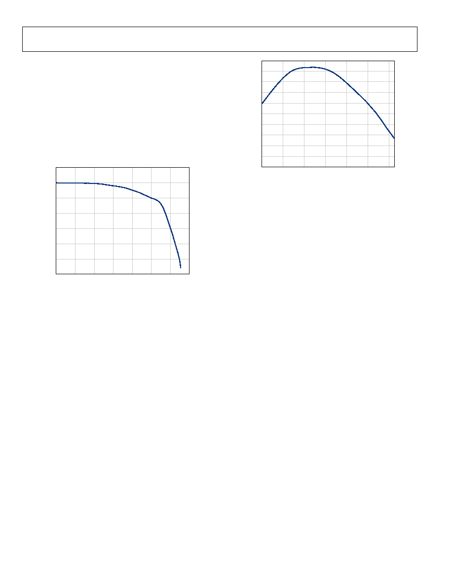
AD9222
Rev. 0 | Page 28 of 56
External Reference Operation
The use of an external reference may be necessary to enhance
the gain accuracy of the ADC or improve thermal drift charac-
teristics. Figure 61 shows the typical drift characteristics of the
internal reference in 1 V mode.
When the SENSE pin is tied to AVDD, the internal reference is
disabled, allowing the use of an external reference. The external
reference is loaded with an equivalent 6 k load. An internal
reference buffer generates the positive and negative full-scale
references, REFT and REFB, for the ADC core. Therefore, the
external reference must be limited to a nominal of 1.0 V.
0
1.0
0.5
2.0
1.5
3.0
2.5
3.5
V
REF
E
R
RO
R
(
%
)
CURRENT LOAD (mA)
05
72
7-
08
3
30
5
10
15
20
25
5
0
Figure 60. V
REF
Accuracy vs. Load, AD9222-50
0.02
0.18
0.14
0.10
0.06
0.02
0.16
0.12
0.08
0.04
0
40
V
REF
E
R
RO
R
(
%
)
TEMPERATURE (°C)
05
96
7-
02
8
20
0
20
40
60
80
Figure 61. Typical V
REF
Drift, AD9222-50

AD9222
Rev. 0 | Page 29 of 56
SERIAL PORT INTERFACE (SPI)
The AD9222 serial port interface allows the user to configure
the converter for specific functions or operations through a
structured register space provided inside the ADC. This gives
the user added flexibility and customization depending on the
application. Addresses are accessed via the serial port and can
be written to or read from via the port. Memory is organized
into bytes that can be further divided down into fields, as doc-
umented in the Memory Map section. Detailed operational
information can be found in the Analog Devices, Inc., user
manual Interfacing to High Speed ADCs via SPI.
There are three pins that define the serial port interface, or SPI,
to this particular ADC. They are the SCLK, SDIO, and CSB
pins. The SCLK (serial clock) is used to synchronize the read
and write data presented to the ADC. The SDIO (serial data
input/output) is a dual-purpose pin that allows data to be sent
to and read from the internal ADC memory map registers. The
CSB (chip select bar) is an active low control that enables or
disables the read and write cycles (see Table 13).
Table 13. Serial Port Pins
Pin Function
SCLK
Serial Clock. The serial shift clock in. SCLK is used to
synchronize serial interface reads and writes.
SDIO
Serial Data Input/Output. A dual-purpose pin. The
typical role for this pin is an input or output, depending
on the instruction sent and the relative position in the
timing frame.
CSB
Chip Select Bar (Active Low). This control gates the read
and write cycles.
The falling edge of the CSB in conjunction with the rising edge
of the SCLK determines the start of the framing sequence. During
an instruction phase, a 16-bit instruction is transmitted, followed
by one or more data bytes, which is determined by Bit Fields
W0 and W1. An example of the serial timing and its definitions
can be found in Figure 63 and Table 14. In normal operation,
CSB is used to signal to the device that SPI commands are to be
received and processed. When CSB is brought low, the device
processes SCLK and SDIO to process instructions. Normally,
CSB remains low until the communication cycle is complete.
However, if connected to a slow device, CSB can be brought
high between bytes, allowing older microcontrollers enough
time to transfer data into shift registers. CSB can be stalled
when transferring one, two, or three bytes of data. When W0
and W1 are set to 11, the device enters streaming mode and
continues to process data, either reading or writing, until the
CSB is taken high to end the communication cycle. This allows
complete memory transfers without having to provide additional
instructions. Regardless of the mode, if CSB is taken high in the
middle of any byte transfer, the SPI state machine is reset and
the device waits for a new instruction.
In addition to the operation modes, the SPI port can be
configured to operate in different manners. For applications
that do not require a control port, the CSB line can be tied and
held high. This places the remainder of the SPI pins in their
secondary mode as defined in the Serial Port Interface (SPI)
section. CSB can also be tied low to enable 2-wire mode. When
CSB is tied low, SCLK and SDIO are the only pins required for
communication. Although the device is synchronized during
power-up, caution must be exercised when using this mode to
ensure that the serial port remains synchronized with the CSB
line. When operating in 2-wire mode, it is recommended to use
a 1-, 2-, or 3-byte transfer exclusively. Without an active CSB
line, streaming mode can be entered but not exited.
In addition to word length, the instruction phase determines if
the serial frame is a read or write operation, allowing the serial
port to be used to both program the chip and read the contents
of the on-chip memory. If the instruction is a readback operation,
performing a readback causes the serial data input/output (SDIO)
pin to change direction from an input to an output at the
appropriate point in the serial frame.
Data can be sent in MSB- or LSB-first mode. MSB-first mode
is the default at power-up and can be changed by adjusting the
configuration register. For more information about this and
other features, see the user manual Interfacing to High Speed
ADCs via SPI.

AD9222
Rev. 0 | Page 30 of 56
This interface is flexible enough to be controlled by either serial
PROMS or PIC mirocontrollers. This provides the user an
alternative method, other than a full SPI controller, to program
the ADC (see the AN-812 Application Note).
HARDWARE INTERFACE
The pins described in Table 13 compose the physical interface
between the user's programming device and the serial port of
the AD9222. The SCLK and CSB pins function as inputs when
using the SPI interface. The SDIO pin is bidirectional, functioning
as an input during write phases and as an output during readback.
If the user chooses not to use the SPI interface, these pins serve
a dual function and are associated with secondary functions
when the CSB is strapped to AVDD during device power-up.
See the Theory of Operation section for details on which pin-
strappable functions are supported on the SPI pins.
If multiple SDIO pins share a common connection, care should
be taken to ensure that proper V
OH
levels are met. Assuming the
same load as the AD9222, Figure 62 shows the number of SDIO
pins that can be connected together and the resulting V
OH
level.
05
96
7-
03
7
NUMBER OF SDIO PINS CONNECTED TOGETHER
V
OH
1.715
1.720
1.725
1.730
1.735
1.740
1.745
1.750
1.755
1.760
1.765
1.770
1.775
1.780
1.785
1.790
1.795
1.800
0
30
20
10
40
50
60
70
80
90
100
Figure 62. SDIO Pin Loading
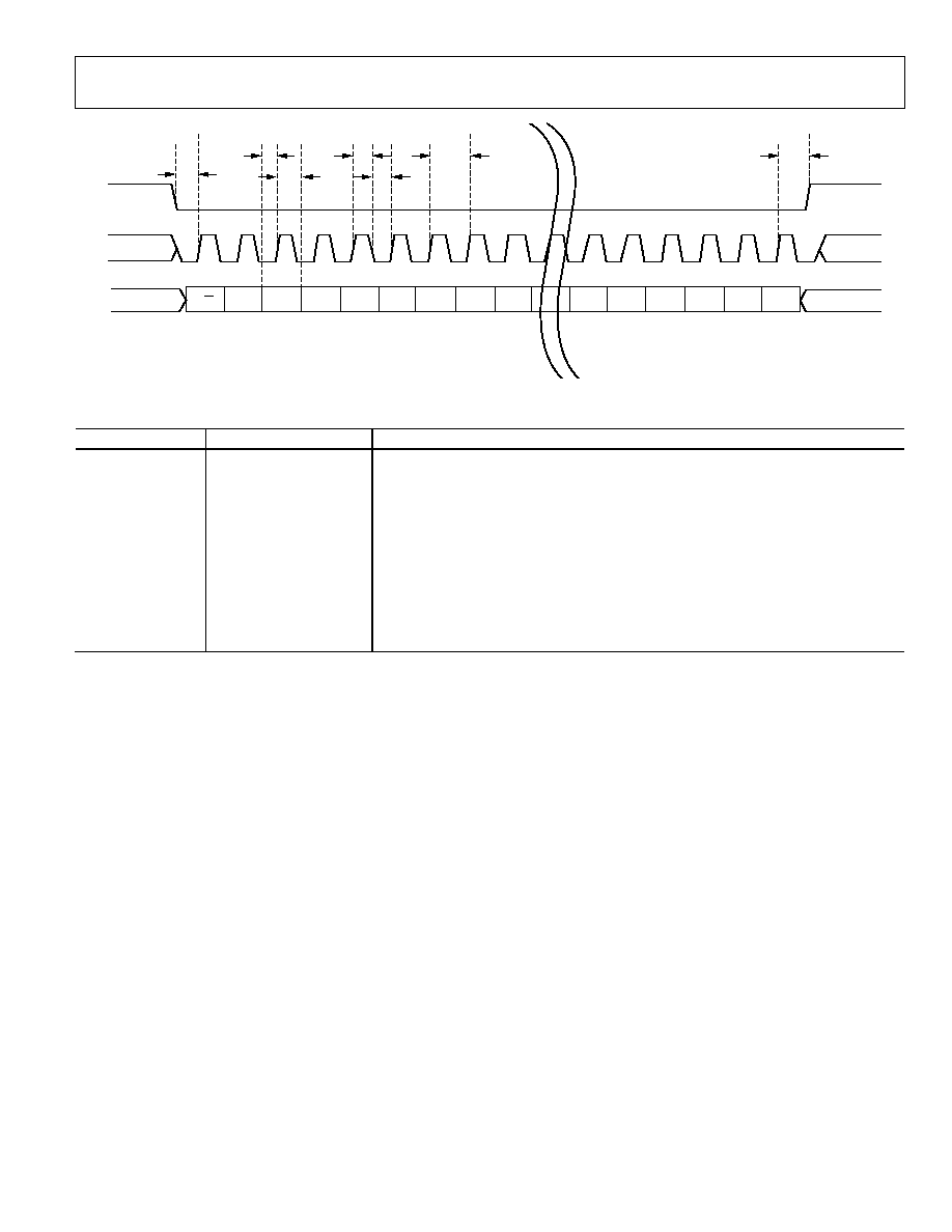
AD9222
Rev. 0 | Page 31 of 56
DON'T CARE
DON'T CARE
DON'T CARE
DON'T CARE
SDIO
SCLK
CSB
t
S
t
DH
t
HI
t
CLK
t
LO
t
DS
t
H
R/W
W1
W0
A12
A11
A10
A9
A8
A7
D5
D4
D3
D2
D1
D0
0
5967
-
068
Figure 63. Serial Timing Details
Table 14. Serial Timing Definitions
Parameter
Timing (minimum, ns)
Description
t
DS
5
Set-up time between the data and the rising edge of SCLK
t
DH
2
Hold time between the data and the rising edge of SCLK
t
CLK
40
Period of the clock
t
S
5
Set-up time between CSB and SCLK
t
H
2
Hold time between CSB and SCLK
t
HI
16
Minimum period that SCLK should be in a logic high state
t
LO
16
Minimum period that SCLK should be in a logic low state
t
EN_SDIO
1
Minimum time for the SDIO pin to switch from an input to an output relative to the SCLK
falling edge (not shown in Figure 63)
t
DIS_SDIO
5
Minimum time for the SDIO pin to switch from an output to an input relative to the SCLK
rising edge (not shown in Figure 63)

AD9222
Rev. 0 | Page 32 of 56
MEMORY MAP
READING THE MEMORY MAP TABLE
Each row in the memory map table has eight address locations.
The memory map is roughly divided into three sections: chip
configuration register map (Address 0x00 to Address 0x02), device
index and transfer register map (Address 0x05 and Address 0xFF),
and program register map (Address 0x08 to Address 0x25).
The left-hand column of the memory map indicates the register
address number in hexadecimal. The default value of this address is
shown in hexadecimal in the right-hand column. The Bit 7 (MSB)
column is the start of the default hexadecimal value given. For
example, Hexadecimal Address 0x09, Clock, has a hexadecimal
default value of 0x01. This means Bit 7 = 0, Bit 6 = 0, Bit 5 = 0,
Bit 4 = 0, Bit 3 = 0, Bit 2 = 0, Bit 1 = 0, and Bit 0 = 1, or 0000 0001
in binary. This setting is the default for the duty cycle stabilizer in
the on condition. By writing a 0 to Bit 6 at this address, the duty
cycle stabilizer turns off. For more information on this and other
functions, consult the user manual Interfacing to High Speed
ADCs via SPI.
RESERVED LOCATIONS
Undefined memory locations should not be written to except
when writing the default values suggested in this data sheet.
Addresses that have values marked as 0 should be considered
reserved and have a 0 written into their registers during power-up.
DEFAULT VALUES
Coming out of reset, critical registers are preloaded with default
values. These values are indicated in Table 15, where an X refers
to an undefined feature.
LOGIC LEVELS
An explanation of various registers follows: "Bit is set" is
synonymous with "bit is set to Logic 1" or "writing Logic 1 for
the bit." Similarly, "clear a bit" is synonymous with "bit is set to
Logic 0" or "writing Logic 0 for the bit."
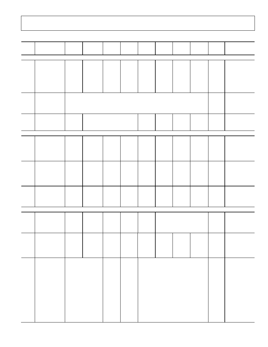
AD9222
Rev. 0 | Page 33 of 56
Table 15. Memory Map Register
Addr.
(Hex)
Parameter Name
Bit 7
(MSB)
Bit 6
Bit 5
Bit 4
Bit 3
Bit 2
Bit 1
Bit 0
(LSB)
Default
Value
(Hex)
Default Notes/
Comments
Chip Configuration Registers
00 chip_port_config
0
LSB
first
1 = on
0 = off
(default)
Soft
reset
1 = on
0 = off
(default)
1 1 Soft
reset
1 = on
0 = off
(default)
LSB first
1 = on
0 = off
(default)
0 0x18
The
nibbles
should be
mirrored so that
LSB- or MSB-first
mode registers
correctly
regardless of
shift mode.
01
chip_id
8-bit Chip ID Bits 7:0
(AD9222 = 0x07), (default)
Read
only
Default is unique
chip ID, different
for each device.
This is a read-
only register.
02
chip_grade
X
Child ID 6:4
(identify device variants of Chip ID)
011 = 50 MSPS
001 = 40 MSPS
X X X X Read
only
Child ID used to
differentiate
graded devices.
Device Index and Transfer Registers
04 device_index_2
X
X
X
X
Data
Channel
H
1 = on
(default)
0 = off
Data
Channel
G
1 = on
(default)
0 = off
Data
Channel
F
1 = on
(default)
0 = off
Data
Channel
E
1 = on
(default)
0 = off
0x0F
Bits are set to
determine which
on-chip device
receives the next
write command.
05 device_index_1
X
X
Clock
Channel
DCO
1 = on
0 = off
(default)
Clock
Channel
FCO
1 = on
0 = off
(default)
Data
Channel
D
1 = on
(default)
0 = off
Data
Channel
C
1 = on
(default)
0 = off
Data
Channel
B
1 = on
(default)
0 = off
Data
Channel
A
1 = on
(default)
0 = off
0x0F
Bits are set to
determine which
on-chip device
receives the next
write command.
FF
device_update
X X X X X X X SW
transfer
1 = on
0 = off
(default)
0x00 Synchronously
transfers data
from the master
shift register to
the slave.
ADC Functions
08
modes
X
X
X
X
X
Internal power-down mode
000 = chip run (default)
001 = full power-down
010 = standby
011 = reset
0x00 Determines
various generic
modes of chip
operation.
09
clock
X X X X X X X Duty
cycle
stabilizer
1 = on
(default)
0 = off
0x01 Turns
the
internal duty
cycle stabilizer
on and off.
0D
test_io
User test mode
00 = off (default)
01 = on, single alternate
10 = on, single once
11 = on, alternate once
Reset PN
long gen
1 = on
0 = off
(default)
Reset
PN short
gen
1 = on
0 = off
(default)
Output test mode--see Table 9 in the
Digital Outputs and Timing section
0000 = off (default)
0001 = midscale short
0010 = +FS short
0011 = -FS short
0100 = checker board output
0101 = PN 23 sequence
0110 = PN 9
0111 = one/zero word toggle
1000 = user input
1001 = one/zero bit toggle
1010 = 1× sync
1011 = one bit high
1100 = mixed bit frequency
(format determined by output_mode)
0x00
When set, the
test data is
placed on the
output pins in
place of normal
data.
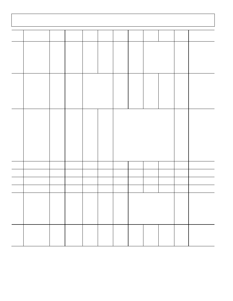
AD9222
Rev. 0 | Page 34 of 56
Addr.
(Hex)
Parameter Name
Bit 7
(MSB)
Bit 6
Bit 5
Bit 4
Bit 3
Bit 2
Bit 1
Bit 0
(LSB)
Default
Value
(Hex)
Default Notes/
Comments
14
output_mode
X
0 = LVDS
ANSI
(default)
1 = LVDS
low
power,
(IEEE
1596.3
similar)
X X X Output
invert
1 = on
0 = off
(default)
00 = offset binary
(default)
01 = twos
complement
0x00 Configures
the
outputs and the
format of the
data.
15 output_adjust X
X
Output driver
termination
00 = none (default)
01 = 200
10 = 100
11 = 100
X
X
X
DCO and
FCO
2× Drive
Strength
1 = on
0 = off
(default)
0x00 Determines
LVDS or other
output properties.
Primarily func-
tions to set the
LVDS span and
common-mode
levels in place of
an external
resistor.
16 output_phase X
X
X
X
0011 = output clock phase adjust
(0000 through 1010)
(Default: 180° relative to DATA edge)
0000 = 0° relative to DATA edge
0001 = 60° relative to DATA edge
0010 = 120° relative to DATA edge
0011 = 180° relative to DATA edge
0100 = 240° relative to DATA edge
0101 = 300° relative to DATA edge
0110 = 360° relative to DATA edge
0111 = 420° relative to DATA edge
1000 = 480° relative to DATA edge
1001 = 540° relative to DATA edge
1010 = 600° relative to DATA edge
1011 to 1111 = 660° relative to DATA edge
0x03
On devices that
utilize global
clock divide,
determines
which phase of
the divider
output is used to
supply the
output clock.
Internal latching
is unaffected.
19
user_patt1_lsb
B7 B6 B5 B4 B3 B2 B1 B0 0x00
User-defined
pattern, 1 LSB.
1A user_patt1_msb
B15 B14
B13 B12 B11 B10 B9 B8 0x00
User-defined
pattern, 1 MSB.
1B
user_patt2_lsb
B7 B6 B5 B4 B3 B2 B1 B0 0x00
User-defined
pattern, 2 LSB.
1C user_patt2_msb
B15 B14
B13 B12 B11 B10 B9 B8 0x00
User-defined
pattern, 2 MSB.
21 serial_control LSB
first
1 = on
0 = off
(default)
X X
X
<10
MSPS,
low
encode
rate
mode
1 = on
0 = off
(default)
000 = 12 bits (default, normal bit
stream)
001 = 8 bits
010 = 10 bits
011 = 12 bits
100 = 14 bits
0x00 Serial
stream
control. Default
causes MSB first
and the native
bit stream
(global).
22
serial_ch_stat
X X X X X X Channel
output
reset
1 = on
0 = off
(default)
Channel
power-
down
1 = on
0 = off
(default)
0x00
Used to power
down individual
sections of a
converter (local).
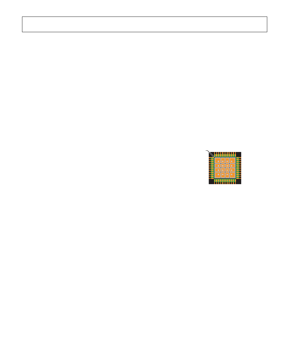
AD9222
Rev. 0 | Page 35 of 56
Power and Ground Recommendations
When connecting power to the AD9222, it is recommended
that two separate 1.8 V supplies be used: one for analog (AVDD)
and one for digital (DRVDD). If only one supply is available, it
should be routed to the AVDD first and then tapped off and
isolated with a ferrite bead or a filter choke preceded by
decoupling capacitors for the DRVDD. The user can employ
several different decoupling capacitors to cover both high and
low frequencies. These should be located close to the point of
entry at the PC board level and close to the parts with minimal
trace length.
A single PC board ground plane should be sufficient when
using the AD9222. With proper decoupling and smart parti-
tioning of the PC board's analog, digital, and clock sections,
optimum performance is easily achieved.
Exposed Paddle Thermal Heat Slug Recommendations
It is required that the exposed paddle on the underside of the
ADC is connected to analog ground (AGND) to achieve the
best electrical and thermal performance of the AD9222. An
exposed continuous copper plane on the PCB should mate to
the AD9222 exposed paddle, Pin 0. The copper plane should
have several vias to achieve the lowest possible resistive thermal
path for heat dissipation to flow through the bottom of the PCB.
These vias should be solder filled or plugged.
To maximize the coverage and adhesion between the ADC and
PCB, partition the continuous copper plane by overlaying a
silkscreen on the PCB into several uniform sections. This provides
several tie points between the two during the reflow process.
Using one continuous plane with no partitions only guarantees
one tie point between the ADC and PCB. See Figure 64 for a
PCB layout example. For detailed information on packaging
and the PCB layout of chip scale packages, see the AN-772
Application Note, A Design and Manufacturing Guide for the
Lead Frame Chip Scale Package (LFCSP), at
www.analog.com
.
SILKSCREEN PARTITION
PIN 1 INDICATOR
059
67-
06
9
Figure 64. Typical PCB Layout
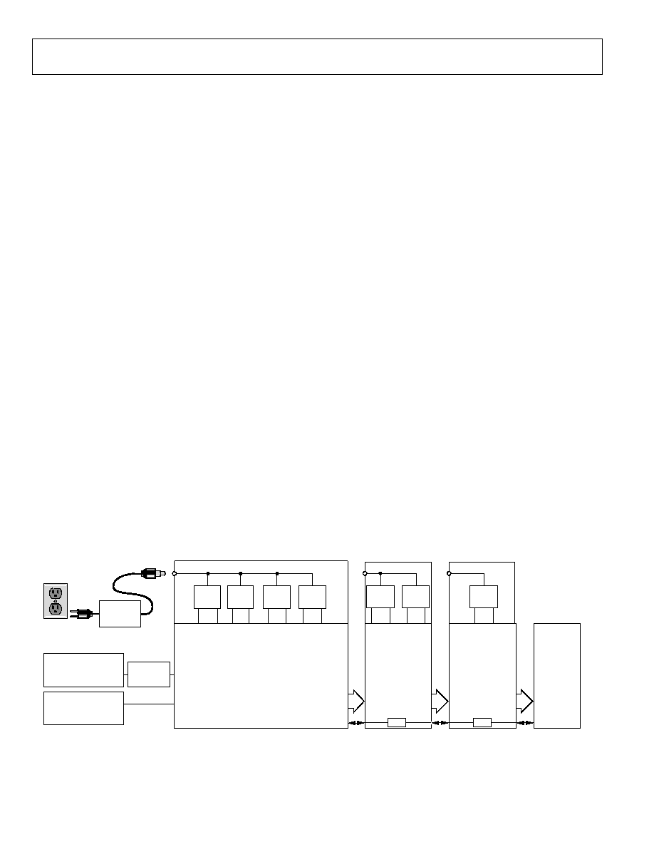
AD9222
Rev. 0 | Page 36 of 56
EVALUATION BOARD
The AD9222 evaluation board provides all of the support cir-
cuitry required to operate the ADC in its various modes and
configurations. The converter can be driven differentially through a
transformer (default) or through the AD8334 driver. The ADC
can also be driven in a single-ended fashion. Separate power pins
are provided to isolate the DUT from the AD8334 drive circuitry.
Each input configuration can be selected by proper connection
of various jumpers (see Figure 67 to Figure 71). Figure 65 shows
the typical bench characterization setup used to evaluate the ac
performance of the AD9222. It is critical that the signal sources
used for the analog input and clock have very low phase noise
(<1 ps rms jitter) to realize the optimum performance of the
converter. Proper filtering of the analog input signal to remove
harmonics and lower the integrated or broadband noise at the
input is also necessary to achieve the specified noise performance.
See Figure 67 to Figure 77 for the complete schematics and
layout diagrams that demonstrate the routing and grounding
techniques that should be applied at the system level.
POWER SUPPLIES
This evaluation board comes with a wall-mountable switching
power supply that provides a 6 V, 2 A maximum output. Simply
connect the supply to the rated 100 V ac to 240 V ac wall outlet
at 47 Hz to 63 Hz. The other end is a 2.1 mm inner diameter
jack that connects to the PCB at P701. Once on the PC board,
the 6 V supply is fused and conditioned before connecting to
three low dropout linear regulators that supply the proper bias
to each of the various sections on the board.
When operating the evaluation board in a nondefault condition,
L701 to L704 can be removed to disconnect the switching
power supply. This enables the user to bias each section of the
board individually. Use P702 to connect a different supply for
each section. At least one 1.8 V supply is needed with a 1 A current
capability for AVDD_DUT and DRVDD_DUT; however, it is
recommended that separate supplies be used for both analog
and digital. To operate the evaluation board using the VGA
option, a separate 5.0 V analog supply is needed. The 5.0 V
supply, or AVDD_5 V, should have a 1 A current capability. To
operate the evaluation board using the SPI and alternate clock
options, a separate 3.3 V analog supply is needed in addition to
the other supplies. The 3.3 V supply, or AVDD_3.3 V, should
have a 1 A current capability as well.
INPUT SIGNALS
When connecting the clock and analog source, use clean signal
generators with low phase noise, such as Rohde & Schwarz SMHU
or HP8644 signal generators or the equivalent. Use a 1 m, shielded,
RG-58, 50 coaxial cable for making connections to the evalu-
ation board. Enter the desired frequency and amplitude from the
ADC specifications tables. Typically, most Analog Devices
evaluation boards can accept ~2.8 V p-p or 13 dBm sine wave
input for the clock. When connecting the analog input source, it
is recommended to use a multipole, narrow-band, band-pass
filter with 50 terminations. Analog Devices uses TTE, Allen
Avionics, and K&L types of band-pass filters. The filter should
be connected directly to the evaluation board if possible.
OUTPUT SIGNALS
The default setup uses the HSC-ADC-FPGA high speed
deserialization board to deserialize the digital output data and
convert it to parallel CMOS. These two channels interface
directly with the Analog Devices standard dual-channel FIFO
data capture board (HSC-ADC-EVALA-DC). Two of the eight
channels can then be evaluated at the same time. For more
information on channel settings on these boards and their
optional settings, visit www.analog.com/FIFO.
ROHDE & SCHWARZ,
SMHU,
2V p-p SIGNAL
SYNTHESIZER
ROHDE & SCHWARZ,
SMHU,
2V p-p SIGNAL
SYNTHESIZER
BAND-PASS
FILTER
XFMR
INPUT
CLK
CHA TO CHH
12-BIT
SERIAL
LVDS
2-CH
12-BIT
PARALLEL
CMOS
USB
CONNECTION
AD9222
EVALUATION BOARD
HSC-ADC-FPGA
HIGH SPEED
DESERIALIZATION
BOARD
HSC-ADC-EVALA-DC
FIFO DATA
CAPTURE
BOARD
PC
RUNNING
ADC
ANALYZER
AND SPI
USER
SOFTWARE
1.8V
+
+
A
V
DD_DU
T
A
V
DD_3.
3V
D
R
V
DD_DU
T
GN
D
GN
D
+
5.0V
GN
D
A
V
DD_5V
1.8V
6V DC
2A MAX
WALL OUTLET
100V TO 240V AC
47Hz TO 63Hz
SWITCHING
POWER
SUPPLY
+
GN
D
3.3V
+
1.
5V
_
F
P
G
A
3.
3
V
_D
GN
D
3.3V
+
GN
D
1.5V
+
VC
C
GN
D
3.3V
SPI
SPI
SPI
SPI
0
59
67
-
0
70
Figure 65. Evaluation Board Connection
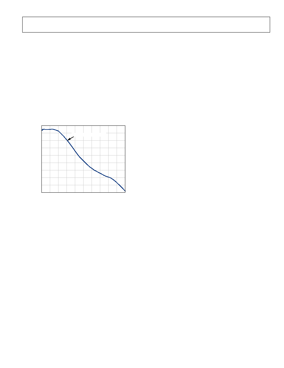
AD9222
Rev. 0 | Page 37 of 56
DEFAULT OPERATION AND JUMPER SELECTION
SETTINGS
The following is a list of the default and optional settings or
modes allowed on the AD9222 Rev. A evaluation board.
· POWER: Connect the switching power supply that is
supplied in the evaluation kit between a rated 100 V ac
to 240 V ac wall outlet at 47 Hz to 63 Hz and P701.
· AIN: The evaluation board is set up for a transformer-
coupled analog input with optimum 50 impedance
matching out to 150 MHz (see Figure 66). For more
bandwidth response, the differential capacitor across the
analog inputs can be changed or removed. The common
mode of the analog inputs is developed from the center
tap of the transformer or AVDD_DUT/2.
0
AM
P
L
I
T
UD
E
(
d
BF
S
)
FREQUENCY (MHz)
0
18
16
14
12
10
8
6
4
2
50
100
150
200
250
300
350
400
450
500
3dB CUTOFF = 150MHz
0
59
67
-
07
1
Figure 66. Evaluation Board Full Power Bandwidth, AD9222-50
· VREF: VREF is set to 1.0 V by tying the SENSE pin to
ground, R317. This causes the ADC to operate in 2.0 V p-p
full-scale range. A separate external reference option using
the ADR510 or ADR520 is also included on the evaluation
board. Simply populate R312 and R313 and remove C307.
Proper use of the VREF options is noted in the Voltage
Reference section.
· RBIAS: RBIAS has a default setting of 10 k (R301) to
ground and is used to set the ADC core bias current. To
further lower the core power (excluding the LVDS driver
supply) simply change the resistor setting. However,
performance of the ADC will degrade depending on the
resistor chosen. See RBIAS section for more information.
· CLOCK: The default clock input circuitry is derived from a
simple transformer-coupled circuit using a high bandwidth
1:1 impedance ratio transformer (T401) that adds a very
low amount of jitter to the clock path. The clock input is
50 terminated and ac-coupled to handle single-ended
sine wave types of inputs. The transformer converts the
single-ended input to a differential signal that is clipped
before entering the ADC clock inputs.
A differential LVPECL clock can also be used to clock the
ADC input using the AD9515 (U401). Simply populate
R406 and R407 with 0 resistors and remove R215 and
R216 to disconnect the default clock path inputs. In addition,
populate C205 and C206 with a 0.1 F capacitor and remove
C409 and C410 to disconnect the default cloth path outputs.
The AD9515 has many pin-strappable options that are set
to a default working condition. Consult the AD9515 data
sheet for more information about these and other options.
If using an oscillator, two oscillator footprint options are
also available (OSC401) to check the ADC performance.
J401 gives the user flexibility in using the enable pin, which
is common on most oscillators.
· PDWN: To enable the power-down feature, simply short
J301 to the on position (AVDD) on the PDWN pin.
· SCLK/DTP: To enable a digital test pattern on the digital
outputs of the ADC, use J304. If J304 is tied to AVDD during
device power-up, Test Pattern 1000 0000 0000 will be enabled.
See the SCLK/DTP Pin section for details.
· SDIO/ODM: To enable the low power, reduced signal option
similar to the IEEE 1595.3 reduced range link LVDS output
standard, use J303. If J303 is tied to AVDD during device
power-up, it enables the LVDS outputs in a low power,
reduced signal option from the default ANSI standard.
This option changes the signal swing from 350 mV p-p to
200 mV p-p, which reduces the power of the DRVDD supply.
See the SDIO/ODM Pin section for more details.
· CSB: To enable the SPI information on the SDIO and
SCLK pins that is to be processed, simply tie J302 low in
the always enable mode. To ignore the SDIO and SCLK
information, tie J302 to AVDD.
· Non-SPI Mode: For users who wish to operate the DUT
without using SPI, simply remove Jumpers J302, J303, and
J304. This disconnects the CSB, SCLK/DTP, and SDIO/OMD
pins from the control bus, allowing the DUT to operate in
its simplest mode. Each of these pins has internal termination
and will float to its respective level.
· D+, D-: If an alternative data capture method to the setup
described in Figure 67 is used, optional receiver terminations,
R318, R320 to R328, can be installed next to the high speed
backplane connector.

AD9222
Rev. 0 | Page 38 of 56
ALTERNATIVE ANALOG INPUT DRIVE
CONFIGURATION
The following is a brief description of the alternative analog
input drive configuration using the AD8334 dual VGA. If this
particular drive option is in use, some components may need to
be populated, in which case all the necessary components are
listed in Table 16. For more details on the AD8334 dual VGA,
including how it works and its optional pin settings, consult the
AD8334 data sheet.
To configure the analog input to drive the VGA instead of the
default transformer option, the following components need to
be removed and/or changed.
· Remove R102, R115, R128, R141, R202, R218, R234, R252,
T101, T102, T103, T104, T201, T202, T203, and T204 in
the default analog input path.
· Populate R101, R114, R127, R140, R201, R217, R233 and
R251 with 0 resistors in the analog input path.
· Populate R106, R107, R119, R120, R132, R133, R144, R145,
R206, R207, R223, R224, R239, R240, R257 and R258 with
10 k resistors to provide an input common-mode level to
the analog input.
· Populate R105, R113, R118, R124, R131, R137, R151, and
R160, R205, R213, R221, R222, R255, R256 with 0 resistors
in the analog input path.
Currently, L505 to L520 and L605 to L620 are populated with 0
resistors to allow signal connection. This area allows the user to
design a filter if additional requirements are necessary.
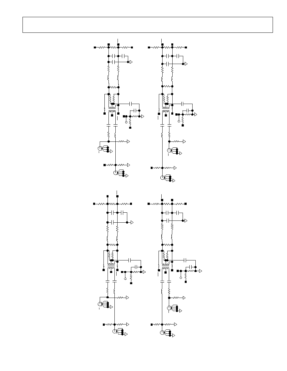
AD9222
Rev. 0 | Page 39 of 56
DN
P
DN
P
DN
P
V
G
A
I
nput
Ai
n
Ai
n
Ain
V
G
A
I
nput
V
G
A
I
nput
C
onne
c
t
i
on
C
onne
c
t
i
on
C
onn
ec
t
i
on
C
onn
ec
t
i
on
V
G
A
I
nput
C
hanne
l
C
Ai
n
DN
P
Ai
n
C
hanne
l
A
Ai
n
Ai
n
C
ha
nnel
B
Ai
n
C
hannel
D
R1
3
4
33
P
105
P1
0
2
R1
4
8
1k
R1
6
0
0
-
DN
P
R
151
0
-
DN
P
R
137
0
-
DN
P
R1
3
1
0
-
DN
P
R1
2
4
0
-
DN
P
R1
1
8
0
-
DN
P
R
113
0
-
DN
P
R
105
0
-
DN
P
R
101
0
-
DN
P
R1
4
0
0
-
DN
P
R1
2
7
0
-
DN
P
R
114
0
-
DN
P
R
107 DN
P
1
2
5
6
T
104
1
2
34
34
5
6
T1
0
3
CM
3
1
2
5
6
T
101
1
2
34
3
4
5
6
T
102
1
E1
0
2
1
E
101
DN
P
C1
2
7
10
F
B
112
10
FB
1
1
1
10
FB
1
1
0
10
FB
1
0
9
10
FB
1
0
8
10
F
B
107
10
F
B
106
10
F
B
105
10
FB
1
0
4
DN
P
C
113
10
F
B
103
10
F
B
102
10
FB
1
0
1
DN
P
C
106
2.
2
p
F
C
118
DN
P
C
124
VI
N
_
D
0.
1
µ
F
C1
1
4
0.
1µ
F
C1
0
7
VI
N
_
D
VI
N
_
C
VI
N
_
B
VI
N
_
B
AV
DD
_
D
UT
AV
DD
_
D
UT
CM
2
CM
1
CH
_
D
CH
_
D
CM
3
CM
1
IN
H
4
IN
H
3
IN
H
1
CH
_
A
CH
_
A
CH
_
C
CM
4
AV
D
D
_
D
U
T
AVD
D
_
D
U
T
AVD
D
_
D
U
T
CM
4
AVD
D
_
D
U
T
IN
H
2
CH
_
B
CH
_
B
CM
2
CH
_
C
R
104
0
R
116
0
R
130
0
R1
4
3
0
AV
DD
_
D
UT
A
V
DD_
DU
T
AV
D
D
_
D
UT
AV
D
D
_
D
U
T
AVD
D
_
D
U
T
AV
DD
_
D
UT
DN
P
C1
2
0
0.
1µF
C1
2
8
0.
1µ
F
C
121
0.
1
µ
F
C1
0
1
2.
2
pF
C1
2
5
DN
P
C
117
DN
P
C
126
DN
P
C
119
DN
P
C1
1
2
0.
1
µ
F
C
108
0.
1
µ
F
C
109
0.
1
µ
F
C1
1
6
0.
1µ
F
C1
1
5
0.
1µF
C1
2
2
0.
1
µ
F
C1
2
3
DN
P
C
110
2
.
2pF
C
111
DN
P
C
103
2.
2
pF
C1
0
4
DN
P
C
105
0.
1µF
C
102
VI
N
_
A
VI
N
_
A
CM
1
CM
2
1
E
103
1
E
104
CM
3
CM
4
R1
3
5
1k
R
123
1k
R
109
1k
49
9
R1
6
4
R
163
499
R
162
49
9
499
R
161
DN
P
R1
5
9
DN
P
R1
5
8
DN
P
R1
5
7
R1
5
6
DN
P
R
108
33
DN
P
R1
5
2
DN
P
R1
5
5
DN
P
R1
5
4
DN
P
R1
5
3
R
102
64.
9
R1
4
7
33
R1
4
6
33
R1
4
5
DN
P
R
149
1k
R
136
33
R1
3
3
DN
P
R1
3
2
DN
P
R1
2
5
1K
R
122
33
R
121
33
R
111
1k
R
106
DN
P
R
112
1k
R1
5
0
1k
R1
3
9
1k
R1
3
8
1k
R
126 1k
R
110
33
R1
4
1
64.
9
R1
4
2
0
R1
2
8
64.
9
R1
2
9
0
R
115
64
.
9
R
117
0
R
103
0
R1
4
4
DN
P
R1
2
0
DN
P
R
119
DN
P
P
101
P
106
P
108
P1
0
7
P
104
P1
0
3
VI
N
_
C
05967-
072
D
N
P:
D
O
N
O
T
PO
PU
L
A
TE.
Figure 67. Evaluation Board Schematic, DUT Analog Inputs
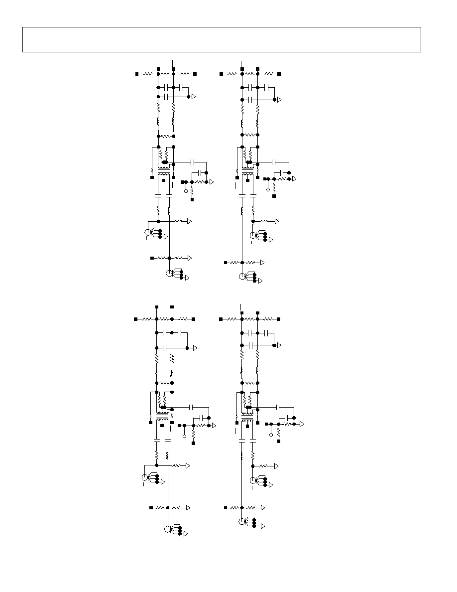
AD9222
Rev. 0 | Page 40 of 56
DN
P
DN
P
DN
P
DN
P
V
G
A
I
nput
Ain
Ai
n
Ai
n
Ain
V
G
A
I
nput
V
G
A
I
nput
V
G
A
I
nput
Ai
n
C
onnec
t
i
o
n
C
onnec
t
i
o
n
C
on
nec
t
i
on
C
onne
c
t
i
on
C
hann
el
E
DN
P
Ai
n
C
hanne
l
G
Ai
n
C
hanne
l
H
C
ha
nnel
F
Ai
n
1
25
6
T2
0
4
R
266
1k
10
F
B
212
R
265
1k
10
FB
2
0
9
10
FB
2
0
7
R
245
33
R
240 DN
P
1
25
34
34
6
T
203
2.
2pF
C
211
R
231
1k
10
FB
2
0
6
10
FB
2
0
3
1
25
6
T
202
R
220
0
R2
5
7
DN
P
R2
5
8
DN
P
R
224 DN
P
R
223
DN
P
2.
2pF
C
204
R2
0
7
DN
P
R
206
DN
P
1
25
34
34
6
T2
0
1
10
F
B
201
R2
6
2
1k
R2
5
6
0
-
DN
P
R
255
0
-
DN
P
R2
3
8
0
-
DN
P
R2
3
7
0
-
DN
P
R
222
0
-
DN
P
R
221
0
-
DN
P
R
213
0
-
DN
P
R2
0
5
0
-
DN
P
R2
0
1
0
-
DN
P
R
251
0
-
DN
P
R
233
0
-
DN
P
R
217
0
-
DN
P
CM
7
1
E
202
1
E
201
DN
P
C
227
10
FB
2
1
1
10
F
B
210
10
F
B
208
10
F
B
205
10
F
B
204
DN
P
C
213
10
FB
2
0
2
DN
P
C
206
2.
2pF
C2
1
8
DN
P
C
224
VI
N
_
H
0.
1
µ
F
C2
1
4
0.
1µ
F
C2
0
7
VI
N
_
H
VI
N
_
G
VI
N
_
G
VI
N
_
F
VI
N
_
F
AV
D
D
_
D
U
T
AV
D
D
_
D
UT
CM
6
CM
5
CH
_
H
CH
_
H
CM
7
CM
5
IN
H
8
IN
H
7
IN
H
5
CH
_
E
CH
_
E
CH
_
G
CM
8
A
V
D
D_
DU
T
AV
D
D
_
D
U
T
AV
D
D
_
D
UT
CM
8
A
V
D
D_
DU
T
IN
H
6
CH
_
F
CH
_
F
CM
6
CH
_
G
R
204
0
R
236
0
R
254
0
AV
DD
_
D
UT
A
V
DD
_
D
UT
AV
D
D
_
D
UT
AV
D
D
_
D
U
T
AVD
D
_
D
U
T
AV
DD
_
D
UT
DN
P
C
220
0.
1µ
F
C2
2
8
0.
1
µ
F
C
221
0.
1µF
C
201
2.
2pF
C2
2
5
DN
P
C2
1
7
DN
P
C2
2
6
DN
P
C
219
DN
P
C
212
0.
1µ
F
C
208
0.
1µ
F
C
209
0
.
1µF
C2
1
6
0.
1
µ
F
C
215
0.
1µ
F
C
222
0.
1
µ
F
C2
2
3
DN
P
C2
1
0
DN
P
C2
0
3
DN
P
C
205
0.
1µ
F
C2
0
2
VI
N
_
E
VI
N
_
E
CM
5
CM
6
1
E
203
1
E
204
CM
7
CM
8
R
246
1k
R
228
1k
R
214
1k
499
R2
5
9
R2
4
1
499
R2
2
5
499
499
R2
0
8
DN
P
R
263
DN
P
R
247
DN
P
R2
2
9
R2
1
5
DN
P
R
209
33
DN
P
R2
1
6
DN
P
R
264
DN
P
R
248
DN
P
R2
3
0
R
202
64
.
9
R
261
33
R
260
33
R2
3
9
DN
P
R
227
33
R
226
33
R2
1
1
1k
R
212
1k
R
250
1k
R
249
1k
R
232 1k
R
210
33
R
242
33
R
252
64
.
9
R
253 0
R
234
64
.
9
k
R
235 0
R
218
64
.
9
R2
1
9
0
R
203 0
P
201
P
202
P
205
P
206
P
208
P
207
P
203
P
204
05967-
073
DN
P
:
DO
N
O
T
P
O
P
U
L
A
T
E
.
Figure 68. Evaluation Board Schematic, DUT Analog Inputs (Continued)
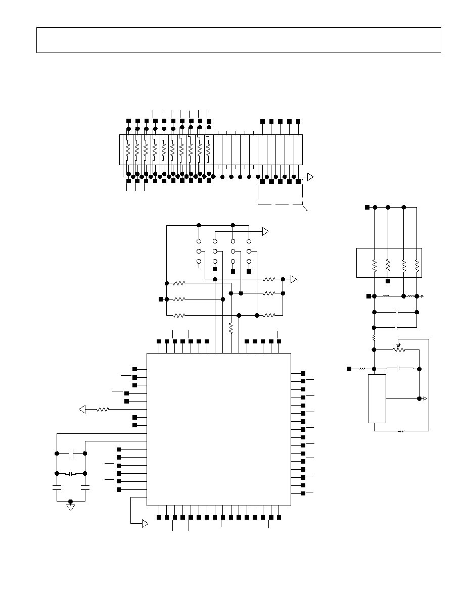
AD9222
Rev. 0 | Page 41 of 56
4.
7
µ
F
CW
GND
VO
UT
TR
I
M
/
N
C
A
D
9222B
CP
Z
-
50
AV
DD
CL
K+
CL
K
-
D+B
D+C
D+D
D+E
D+F
D+G
D+
H
D-B
D-C
D-D
D-E
D-F
D-G
D
-
H
DCO+
DCO-
DRG
ND
DRV
DD
FCO+
FCO-
PDW
N
AV
D
D
RBIAS
REFB
REFT
SCL
K
/
D
T
P
SDI
O
/
O
DM
VI
N+
A
VIN+C
VIN+D
VIN+E
VI
N
+
G
VI
N
-
A
VI
N
-
B
VIN-C
VIN-D
VIN-F
VI
N
-
G
VREF
VIN+F
SLUG
AVDD
AV
D
D
AVDD
DRG
ND
VI
N
-
H
D+
A
D
-
A
VI
N+
B
CSB
SENSE
VIN-E
VI
N
+
H
DRV
DD
AV
D
D
AVDD
AVDD
AVDD
AVDD
AV
DD
AV
D
D
AVDD
A1
A1
0
A2
A3
A4
A5
A6
A7
A8
A9
B1
B1
0
B2
B3
B4
B5
B6
B7
B8
B9
C1
C1
0
C2
C3
C4
C5
C6
C7
C8
C9
D1
D1
0
D2
D3
D4
D5
D6
D7
D8
D9
G
N
D
AB1
GN
D
A
B
1
0
GN
D
A
B
2
GN
D
A
B
3
G
N
D
AB4
GN
D
A
B
5
GN
D
A
B
6
GN
D
A
B
7
G
N
D
AB8
GN
D
A
B
9
G
N
DC
D1
G
N
DC
D1
0
G
N
DC
D2
G
N
DC
D3
G
N
DC
D4
G
N
DC
D5
G
N
DC
D6
G
N
DC
D7
G
N
DC
D8
G
N
DC
D9
O
p
t
i
on
al
O
ut
pu
t
Te
r
m
i
n
a
t
i
o
n
s
Di
g
i
t
a
l
O
u
t
p
u
t
s
us
i
n
g ex
t
e
r
na
l
V
r
ef
V
RE
F
= 1
V
V
RE
F
=
E
x
te
rn
a
l
V
RE
F
= 0
.
5
V
Re
m
o
v
e
C2
1
4
wh
e
n
AL
W
AY
S EN
A
BL
E
SP
I
ODM
E
n
a
b
le
D
T
P
E
nabl
e
V
RE
F
=
0.
5
V
(
1
+
R
2
19
/
R
22
0)
Vr
e
f
S
e
l
e
c
t
1.
0
V
Re
f
e
r
e
n
c
e
De
c
o
u
p
lin
g
OP
T
I
ON
A
L
EX
T REF
P
W
DN
ENAB
L
E
NC
Re
fe
re
n
c
e
C
i
r
c
u
i
t
r
y
R3
1
8
,
R3
2
0
-
R3
2
8
DNP
R3
2
2
CHB
1
10
2
3
4
5
6
7
8
9
11
20
12
13
14
15
16
17
18
19
31
40
32
33
34
35
36
37
38
39
41
50
42
43
44
45
46
47
48
49
21
30
22
23
24
25
26
27
28
29
51
60
52
53
54
55
56
57
58
59
P3
0
1
CHB
DNP
R3
1
8
DNP
R3
2
0
DNP
R3
2
1
DNP
R3
2
3
DNP
R3
2
4
DNP
R3
2
5
DNP
R3
2
8
DNP
R3
2
6
3
2
1
J3
04
1
2
3
J3
03
1
2
3
J3
02
3
2
1
J3
01
R3
1
9
1k
A
V
DD_
DUT
AVDD_DUT
AVDD_DUT
VIN_E
VIN_E
VIN_F
VIN_F
1
59
4
42
45
48
51
62
7
10
9
11
8
32
30
28
22
20
18
16
31
29
27
21
19
17
15
24
23
13
36
14
35
37
26
25
33
34
40
47
55
61
5
6
41
12
54
57
58
38
39
43
49
53
60
2
44
46
50
52
63
3
56
64
0
U3
0
1
R306
100k
R305
100k
R3
0
3
10
0k
DNP
R3
0
4
DNP
R302
S
C
LK
_D
T
P
SDI
O
_
O
DM
CSB_
DUT
0.
1µ
F
C3
0
5
4.
99
k
R3
0
9
1µF
C3
0
7
C3
0
1
0.
1
µ
F
C3
0
4
0.
1µF
C3
0
2
0.
1
µ
F
A
DR5
1
0
ART
Z
U3
0
2
10
k
R3
1
0
DNP
R3
1
1
R307
10k
VSENS
E
_
DUT
47
0k
R3
0
8
DNP
R3
1
3
DNP
R3
1
2
0
R3
1
7
DNP
R3
1
DNP
R3
1
5
DNP
R3
1
4
R301
10k
0.
1µ
F
C3
0
6
AVDD_
DUT
VRE
F
_
DUT
AVDD_DUT
A
V
DD_
DUT
DRV
DD_
DUT
A
V
DD_
DUT
AVDD_DUT
A
V
DD_
DUT
CL
K
CL
K
CHB
CHC
CHD
CHH
CHB
CHC
CHD
CHH
DCO
DCO
GN
D
DRVDD_
DUT
FCO
FCO
VSENSE_DUT
VI
N
_
H
VI
N
_
H
VIN_C
VIN_D
VI
N_
G
VIN_C
VIN_D
VI
N_
G
VREF_DUT
CHG
CHG
CHF
CHF
CHE
CHE
A
V
DD_
DUT
A
V
DD_
DUT
GN
D
A
V
DD_
DUT
VI
N
_
A
VI
N
_
A
CHA
CHA
A
V
DD_
DUT
VI
N
_
B
VI
N
_
B
A
V
DD_
DUT
A
V
DD_
DUT
A
V
DD_
DUT
DNP
R3
2
7
SCL
K
_
CHA
SDI
_
CHA
CSB1
_
CHA
CSB2
_
CHA
SDO
_
CHA
S
CL
K
_
CHB
SDI
_
CHB
CS
B3
_
CHB
CS
B4
_
CHB
S
DO
_
CHB
DCO
FC
O
CHA
CHC
CHD
CHE
CHF
CHG
CHH
CHH
CHG
CHF
CHE
CHD
CHC
CHA
FC
O
DCO
C3
0
3
0596
7-074
DNP:
DO
NO
T
PO
PUL
A
T
E
.
Figure 69. Evaluation Board Schematic, DUT, VREF, and Digital Output Interface
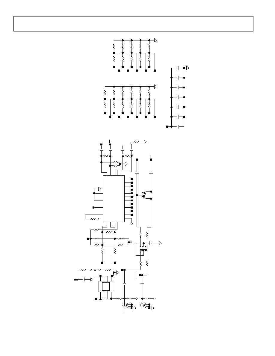
AD9222
Rev. 0 | Page 42 of 56
C
R
YST
A
L
_
3
GN
D
OE
OU
T
VC
C
OE
GN
D
OU
T
VC
C
CL
K
CL
K
B
GND
G
N
D
_
PAD
OU
T
0
OU
T
0
B
OU
T
1
OU
T
1
B
RSET
S0
S1
S10
S2
S3
S4
S5
S6
S7
S8
S9
SY
N
C
B
VREF
VS
S
I
G
N
A
L
=
D
N
C
;
27,
28
DN
P
DN
P
DN
P
DN
P
DN
P
DN
P
DN
P
DN
P
I
npu
t
E
nc
ode
En
c
En
c
Cl
o
c
k
Ci
r
c
u
i
t
DN
P
DN
P
DN
P
DN
P
D
I
S
A
B
LE
O
S
C
401
EN
ABL
E
O
SC
4
0
1
O
pt
i
onal
C
l
oc
k
O
s
c
i
l
l
at
or
A
D
9515 P
i
n
-
s
t
r
ap set
t
i
ngs
O
P
T
I
O
N
AL
C
L
O
C
K DR
I
VE CI
R
C
U
I
T
LV
P
E
C
L O
U
T
P
U
T
DN
P
:
D
O
NO
T
P
O
P
U
L
A
T
E
.
DN
P
DN
P
DN
P
LV
D
S
O
U
T
P
U
T
C
L
IP
S
I
N
E
O
U
T
(
D
E
F
A
U
L
T
)
DN
P
12
6
7
25
8
16
9
15
10
14
11
13
3
2
5
18
19
23
22
32
1
31
33
U4
0
1
S
I
G
N
A
L
=
A
V
D
D
_
3.
3V
;
4,
17,
20,
21,
2
4,
26
,
29,
30
A
D
951
5B
C
P
Z
0
R4
3
0
R4
4
6
0
R4
2
4
R4
2
8
0
R4
2
5
0
R4
2
7
0
1
2
3
J
401
10
12
3
5
7
1
8
14
OS
C
4
0
1
0
R4
2
6
S0
0
R
436
R4
3
7
0
10k
R
413
C4
0
1
0.
1µ
F
R4
0
1
10
k
R
403
0
DN
P
0.
1µ
F
5
1
4
C
2
1
4
C
0.
1µ
F
C4
1
6
C
411
0.
1
µ
F
0
R
406
0
R
415
10
k
R
402
49
.
9
R
411
R
407
0
0
R4
3
4
C4
0
5
0.
1
µ
F
DN
P
0.
1
µ
F
C4
0
6
DN
P
0.
1
µ
F
C4
0
7
DN
P
C4
0
8
0.
1
µ
F
DN
P
R4
4
4
0
0
R4
4
2
R4
4
0
0
0
R4
3
8
R4
3
2
0
0
R4
4
5
R4
4
3
0
0
R4
4
1
R4
3
9
0
R4
3
5
0
0
R4
3
3
R4
3
1
0
0
R4
2
9
S4
1
E4
0
1
AV
D
D
_
3
.
3
V
0
R
416
3
2
1
C
R
401
H
S
M
S
-
2
812-
T
R
1
G
R
414
4.
12k
S5
S3
S2
S1
AVD
D
_
3
.
3
V
R
421 24
0
C4
0
9
0.
1µ
F
R
409
DN
P
24
0
R
420
6
5
4
3
2
1
T
401
0.
1µ
F
C4
0
2
C4
1
0
0.
1
µ
F
49
.
9
R
404
R
410
10k
R
412
DN
P
DN
P
R
408
R
405
0
C4
0
3
0.
1µ
F
10
0
R
423
R
422
100
R4
1
8
0
R4
1
7
0
S0
S1
S2
S3
S4
S5
S6
S7
S8
S9
S1
0
OP
T
_
C
L
K
OP
T
_
C
L
K
CL
K
A
V
D
D
_3.
3V
OP
T
_
C
L
K
OP
T
_
C
L
K
CL
K
CL
K
CL
K
A
V
D
D
_
3.
3V
AVD
D
_
3
.
3
V
AVD
D
_
3
.
3
V
AVD
D
_
3
.
3
V
AVD
D
_
3
.
3
V
A
V
D
D
_3.
3V
AVD
D
_
3
.
3
V
A
V
D
D
_
3.
3V
A
V
D
D
_
3.
3V
A
V
D
D
_
3.
3V
A
V
D
D
_
3.
3V
S6
S7
S8
S9
S1
0
C
413
0.
1µF
0.
1
µ
F
8
1
4
C
4
1
4
C
0.
1µF
0.
1µF
C
417
AV
D
D
_
3
.
3
V
A
V
D
D
_3.
3
V
P
401
P
402
05967
-07
5
0.
1
µ
F
Figure 70. Evaluation Board Schematic, Clock Circuitry
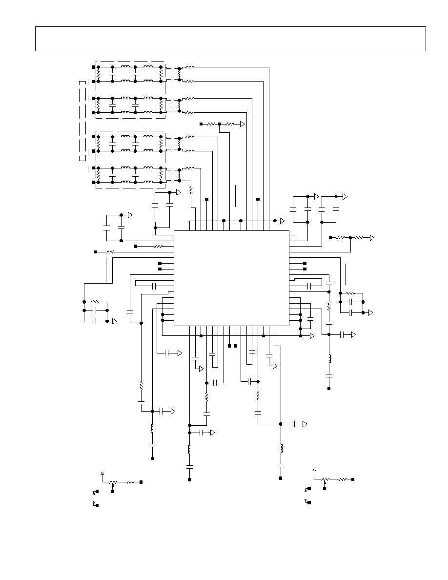
AD9222
Rev. 0 | Page 43 of 56
CW
CW
A
D
833
4A
CP
Z
-
RE
E
L
IN
H
2
LM
D
2
CO
M
2
X
LO
N
2
LO
P
2
VI
P2
VI
N
2
VP
S2
VP
S3
VI
N
3
VI
P3
LO
P
3
LO
N
3
CO
M
3
X
LM
D
3
IN
H
3
COM4
INH4
LMD4
COM4X
LON4
LOP4
VIP4
VIN4
VPS4
HILO
MOD
E
VPS1
VIN1
VIP1
LOP1
LON1
COM1X
LMD1
INH1
COM1
NC
NC
VO
L
2
VO
H
2
COM2
VCM2
COM3
VCM3
VO
L
3
VO
H
3
VCM4
VO
H
4
VO
L
4
VO
L
1
VO
H
1
VCM1
GAIN12
CLMP12
EN12
CO
M
1
2
VP
S1
2
CO
M
1
2
EN34
CO
M
3
4
VP
S3
4
CO
M
3
4
CLMP34
GAIN34
EX
T
V
G
External
Variable Gain Drive
Variable Gain Circuit
(0-1.0V DC)
H
I
LO
P
i
n=
H
=
+
/
-
75m
V
H
I
LO
P
i
n=
L
O
=
+
/
-
50m
V
Rc
l
a
m
p
P
in
EX
T
V
G
H
I
LO
P
i
n=
H
=
+
/
-
75m
V
H
I
LO
P
i
n=
LO
=
+
/
-
50
m
V
Rc
l
a
m
p
Pin
External
Variable Gain Drive
Variable Gain Circuit
(0-1.0V DC)
r
es
i
s
t
or
s
o
r
des
i
gn y
o
ur
ow
n f
i
l
t
er
.
P
o
w
e
r
Do
wn
E
n
a
b
le
(0
-
1V
=
D
i
s
ab
l
e P
ow
er
)
DN
P
:
D
O
NO
T
PO
P
U
L
A
T
E
.
MO
D
E
P
i
n
P
o
si
t
i
ve
G
a
i
n
S
l
o
p
e
=
0
-
1.
0
V
N
egi
t
i
v
e G
ai
n
S
l
ope
=
2.
25
-
5.
0V
P
opul
at
e L505
-
L520 w
i
t
h
0
0.
1µ
F
C5
3
7
0
L519
0
L51
5
374
R5
3
2
374
R
527
DN
P
R5
2
2
DN
P
R
517
0.
1
µ
F
C5
3
0
0.
1µ
F
C5
2
9
0.
1
µ
F
C5
2
8
120nH
L503
0.
1µF
C
524
0.
1
µ
F
C5
2
3
0.
1µ
F
C5
1
8
37
4
R5
1
5
10k
R504
0.
1µ
F
C5
0
4
62
61
60
59
58
57
56
55
54
53
52
51
50
49
33
34
35
36
37
38
39
41
42
43
44
45
46
47
17
18
19
20
21
22
23
24
25
26
27
28
29
30
31
32
16
15
14
13
12
11
10
9
8
7
6
5
4
3
2
1
63
64
48
40
U
501
0.
1µ
F
C
506
AV
D
D
_
5
V
10k
R511
10k
R512
10k
R505
AVDD_5V
AV
D
D
_
5
V
AV
D
D
_
5
V
AVDD_5V
VG34
0.
1µ
F
C5
3
8
AVD
D
_
5
V
AVD
D
_
5
V
0.1µF
C505
22pF
C503
VG12
C512
10µF
AVD
D
_
5
V
AVDD_5V
0.1µF
C501
187
R513
10
k
DN
P
R
506
10k
R
501
274
R503
0.018µF
C502
12
J
P
501
120nH
L501
0.
1µ
F
C5
0
8
0.1µF
C509
1000pF
C
507
39
k
R
502
C510
10µF
AVDD_5V
VG12
VG12
GND
R
521
DN
P
0
L
510
R
516
DN
P
C
542
DN
P
187
R
518
187
R
514
0.
1µ
F
C
545
0.
1
µ
F
C
541
0.
1µ
F
C5
4
0
0
L505
0
L5
1
1
0
L508
0
L5
07
0
L509
0
L506
0
L
512
374
R
520
18
7
R
519
0.
1
µ
F
C5
4
4
C
546
DN
P
C
543
DN
P
C
547
DN
P
CH
_
C
CH
_
D
CH
_
D
CH
_
C
DN
P
R5
3
4
R
533
DN
P
0
L5
1
8
R
528
DN
P
C5
5
0
DN
P
18
7
R
530
18
7
R
526
0.
1
µ
F
C
553
0.
1µ
F
C
549
0.
1µ
F
C5
4
8
0
L
513
0
L51
6
0
L
517
0
L514
0
L520
187
R5
3
1
187
R5
2
5
0.
1µ
F
C
552
C
554
DN
P
C5
5
1
DN
P
C
555
DN
P
DN
P
R5
2
9
CH
_
A
CH
_
B
CH
_
B
CH
_
A
IN
H
4
0.1µF
C511
22pF
C514
0.1µF
C513
120nH
L502
IN
H
3
274
R507
0.018µF
C515
0.
1
µ
F
C
522
22pF
C520
0.1µF
C519
274
R508
0.018µF
C521
IN
H
2
C526
22pF
C525
0.1µF
L504
120nH
R509
274
C527
0.018µF
IN
H
1
0.1µF
0.1µF
C536
C535
C534
C533
10µF
10µF
10k
DN
P
R5
1
0
0.
1µ
F
C
532
1000pF
C
531
10k
R
535
1
J
P
502
39k
R
536
AVDD_5V
VG34
VG34
GND
10k
R523
10k
R524
A
V
D
D
_5V
059
67-0
76
2
Figure 71. Evaluation Board Schematic, Optional DUT Analog Input Drive
AD9222
Rev. 0 | Page 44 of 56
CW
CW
A
D
833
4A
CP
Z
-
RE
E
L
IN
H
2
LM
D
2
CO
M
2
X
LO
N
2
LO
P
2
VI
P
2
VI
N
2
VPS
2
VPS
3
VI
N
3
VI
P
3
LO
P
3
LO
N
3
CO
M
3
X
LM
D
3
IN
H
3
COM4
INH4
LMD4
COM4X
LON4
LOP4
VIP4
VIN4
VPS4
HILO
MO
D
E
VPS1
VIN1
VIP1
LOP1
LON1
COM1X
LMD1
INH1
COM1
NC
NC
VO
L
2
VO
H
2
COM2
VCM2
COM3
VCM3
VO
L
3
VO
H
3
VCM4
VO
H
4
VO
L
4
VO
L
1
VO
H
1
VCM1
GAIN12
CLMP12
EN12
CO
M
1
2
VP
S1
2
CO
M
1
2
EN34
CO
M
3
4
VP
S3
4
CO
M
3
4
CLMP34
GAIN34
MO
D
E
P
i
n
P
o
si
t
i
ve
G
a
i
n
S
l
o
p
e
=
0
-
1.
0
V
N
egat
i
v
e G
ai
n S
l
o
pe
=
2.
25
-
5.
0V
EX
T
V
G
External
Variable Gain Drive
Variable Gain Circuit
(0-1.0V DC)
H
I
LO
P
i
n=
H
=
+
/
-
75m
V
H
I
LO
P
i
n=
LO
=
+
/
-
50m
V
Rc
l
a
m
p
P
in
EXT
VG
H
I
LO
P
i
n=
H
=
+
/
-
75m
V
H
I
LO
P
i
n=
LO
=
+
/
-
50m
V
Rc
l
a
m
p
P
i
n
External
Variable Gain Drive
Variable Gain Circuit
(0-1.0V DC)
P
o
pul
a
t
e L605
-
L620 w
i
t
h 0
r
es
i
s
t
or
s
or
des
i
g
n y
ou
r
ow
n
f
i
l
t
er
.
P
o
we
r
Do
w
n
E
n
a
b
l
e
(0
-
1V
=
D
i
s
ab
l
e P
ow
er
)
DN
P
:
D
O
NO
T
P
O
P
U
L
A
T
E
.
62
61
60
59
58
57
56
55
54
53
52
51
50
49
33
34
35
36
37
38
39
41
42
43
44
45
46
47
17
18
19
20
21
22
23
24
25
26
27
28
29
30
31
32
16
15
14
13
12
11
10
9
8
7
6
5
4
3
2
1
63
64
48
40
U
601
374
R
620
DN
P
R
636
374
R
632
37
4
R
627
DN
P
R
622
0
L
619
0
L61
1
0.
1µF
C
630
0.
1
µ
F
C6
2
9
0.
1µ
F
C6
2
8
0.
1µF
C
624
0.
1µ
F
C6
2
3
0.
1µ
F
C
618
0.
1µ
F
C
616
10k
R604
0.
1µ
F
C6
0
4
10k
R612
10k
R6
2
4
AVDD_5V
A
V
D
D
_5V
AVD
D
_
5
V
AVDD_5V
VG78
0.
1µF
C
617
A
V
D
D
_5V
A
V
D
D
_5V
0.1µF
C605
22pF
C603
0.
1µ
F
C6
0
6
VG56
C612
10µF
AVD
D
_
5
V
AVDD_5V
0.1µF
C601
187
R613
10
k
DN
P
R
606
10k
R6
0
1
274
R603
0.018µF
C602
12
JP
6
0
1
L601
120nH
0.
1µ
F
C6
0
8
0.1µF
C609
10k
R605
1000p
F
C
607
39k
R6
0
2
C610
10µF
AVDD_5V
VG56
VG56
GND
R
621
DN
P
0
L6
10
R
616
DN
P
C6
4
2
DN
P
37
4
R
615
18
7
R
618
187
R
614
0.
1
µ
F
C6
4
5
0.
1µF
C
641
0.
1µF
C
640
0
L605
0
L608
0
L60
7
0
L609
0
L606
0
L
612
187
R
619
0.
1µF
C
644
C
646
DN
P
C6
4
3
DN
P
C
647
DN
P
DN
P
R
617
CH
_
G
CH
_
H
CH
_
H
CH
_
G
R
633
DN
P
0
L
618
R
628
DN
P
C6
5
0
DN
P
187
R
630
187
R6
2
6
0.
1µ
F
C
653
0.
1µ
F
C
649
0.
1
µ
F
C
648
0
L613
0
L61
6
0
L61
5
0
L
617
0
L61
4
0
L620
187
R6
3
1
187
R
625
0.
1
µ
F
C
652
C
654
DN
P
C6
5
1
DN
P
C
655
DN
P
DN
P
R
629
CH
_
E
CH
_
F
CH
_
F
CH
_
E
IN
H
8
0.1µF
C611
22pF
C614
0.1µF
C613
L602
120nH
IN
H
7
274
R607
0.018µF
C615
0.
1µ
F
C6
2
2
22pF
C620
0.1µF
C619
L603
120nH
274
R608
C621
IN
H
6
C626
22pF
C625
0.1µF
L604
120nH
R609
274
C627
0.018µF
IN
H
5
0.1µF
0.1µF
C636
10µF
C634
C633
10µF
10k
DN
P
R
610
0.
1µ
F
C
632
100
0pF
C
631
10k
R
634
12
J
P
602
39k
R
635
AVDD_5V
VG78
VG78
GND
10k
R611
AVD
D
_
5
V
10k
R6
2
3
A
V
D
D
_5V
C635
0596
7-077
0.018µF
Figure 72. Evaluation Board Schematic, Optional DUT Analog Input Drive (Continued)
AD9222
Rev. 0 | Page 45 of 56
NA
NO
S
M
DC
1
1
0
F
-
2
S2
A
-
T
P
GP
0
GP
1
GP
2
GP
4
GP
5
VD
D
VSS
MC
L
R
/
G
P
3
P
I
C
12F
62
9-
I
/
S
N
G
4
Y1
VC
C
Y2
A2
GN
D
A1
CO
N0
0
5
7.
5
V
P
O
W
E
R
2.
5
M
M
J
A
C
K
P1
P2
P3
P4
P5
P6
P7
P8
GND
GND
GND
GND
OU
T
Y1
VC
C
Y2
A2
GN
D
A1
OPTIONAL
+3
.
3
V =
N
O
R
M
A
L
O
PER
AT
I
O
N
=
AV
D
D
_
3
.
3
V
+5
V
= PR
O
G
R
A
M
M
I
N
G
=
A
V
D
D
_
5
V
R
ESE
T
/
R
E
PR
O
G
R
AM
IS
P
PI
C
P
R
O
G
R
AM
M
I
N
G
H
EAD
ER
R
E
M
O
V
E
W
H
E
N
U
S
I
N
G
O
R
P
R
O
G
R
A
M
M
I
N
G
P
I
C
(
U
402)
S
P
I
C
I
R
C
U
I
TR
Y FR
O
M
FI
FO
P
o
w
er
S
uppl
y
I
nput
I
n
put
6V
,
2A
m
ax
+5
.
0
V
DN
P
:
D
O
NO
T
P
O
P
U
L
A
T
E
.
+1
.
8
V
+1
.
8
V
+3
.
3
V
D
ec
oup
l
i
ng C
apac
i
t
o
r
s
O
pt
i
on
al
P
ow
er
D7
0
2
6
5
4
3
2
1
U
703
N
C
7W
Z
16P
6X
_N
L
3.
3
V
_A
V
D
D
5V
_
A
V
D
D
D
U
T
_
AVD
D
DU
T
_
D
RV
D
D
L701 10µ
H
AVD
D
_
5
V
1
2
3
4
U
707
AD
P3
3
3
9
Z
AK
C
-
1.
8
-
R
L
AVD
D
_
5
V
AVD
D
_
D
U
T
CR702
GREEN
MCLR/GP3
CR701
GREEN
4
2
3
1
A
D
P
333
9Z
A
K
C
-
5-
R
L7
U7
0
6
1
2
3
4
U
704
A
D
P
3
339Z
A
K
C
-
1.
8-
R
L
4
2
3
1
A
D
P
3339
Z
A
K
C
-
3.
3-
R
L
U
705
2
43
1
F
E
R
701
1
2
3
4
5
6
7
8
P
702
DN
P
1
3
2
P7
0
1
1
2
34
5
6
N
C
7W
207P
6X
_N
L
U
702
1k
R
713
0
R709
R708
0
0
0
R706
2
4
6
8
10
9
7
5
3
1
J7
0
2
1
2
3
S
701
4
3
7
6
5
2
8
1
U7
0
1
0.
1µF
C
726
0.
1
µ
F
C
742
A
V
D
D_
DU
T
0.
1
µ
F
C7
3
0
D7
0
1
F7
0
1
A
V
D
D
_3.
3V
0.
1µ
F
C
740
0.
1µ
F
C
741
L702 10µ
H
C7
1
0
0.
1µ
F
C
709
10
µ
F
10
µ
H
L
705
R
716
261
10
µ
H
L
706
L704 10µ
H
C
715
1µ
F
0.
1µ
F
C7
0
8
0.
1µ
F
C7
1
2
C7
0
6
0.
1µ
F
C
717
1µ
F
C7
1
6
1µF
C
714 1µ
F
PW
R
_
I
N
PW
R
_
I
N
10
µ
F
C
707
C7
0
5
10µ
F
10µ
F
C7
1
1
DU
T
_
AV
DD
DU
T
_
D
RV
D
D
0.
1
µ
F
C
735
0.
1µ
F
C7
3
4
0.
1µF
C
733
0.
1µ
F
C7
2
7
0.
1µ
F
C
732
0.
1µF
C
731
0.
1
µ
F
C7
4
3
0.
1
µ
F
C7
2
3
0.
1µ
F
C
725
0.
1µF
C
724
10µ
H
L703
5V
_A
V
D
D
3.
3V
_A
V
D
D
PW
R
_
I
N
PW
R
_
I
N
1µ
F
C
719
1µ
F
C
721
1µ
F
C7
2
2
1µ
F
C
720
L7
08
10
µ
H
L707 10
µ
H
DR
V
D
D_
D
UT
1k
R
712
1k
R
710
R707
C7
0
1
0.
1
µ
F
R
715
10k
10k
R7
1
1
0.1µF
C703
R
704
0
-
DN
P
0
-
DN
P
R
703
0
-
DN
P
R
705
261
R
702
3
2
1
J
701
R7
0
1
4.
7
k
1
E
701
C702
0.1µF
10
k
R
714
PICVCC
GP1
GP0
MCLR/GP3
PICVCC
AVD
D
_
D
U
T
AVD
D
_
3
.
3
V
AVD
D
_
5
V
AVD
D
_
D
U
T
SC
L
K_
D
T
P
CS
B_
DU
T
A
V
D
D
_3.
3V
GP0
CSB1_CHA
SCLK_CHA
SDI_CHA
GP1
SDO_CHA
AV
D
D
_
D
UT
SD
I
O
_
O
D
M
PW
R
_
I
N
A
V
D
D
_3.
3V
A
V
D
D
_5V
AV
DD
_
D
UT
DR
V
D
D_
D
UT
0.
1
µ
F
C
744
0.
1µ
F
C
748
0.
1
µ
F
C
747
0.
1µ
F
C
746
0.
1
µ
F
C
745
0.
1µ
F
C
752
0.
1µ
F
C7
5
3
0.
1µ
F
C7
4
9
0.
1µ
F
C7
5
1
0.
1µF
C
750
C7
0
4
10µ
F
059
67-0
78
IN
IN
OU
T
OU
T
OU
T
S
K
33-
T
P
OU
T
IN
IN
OU
T
OU
T
OU
T
Figure 73. Evaluation Board Schematic, Power Supply Inputs and SPI Interface Circuitry
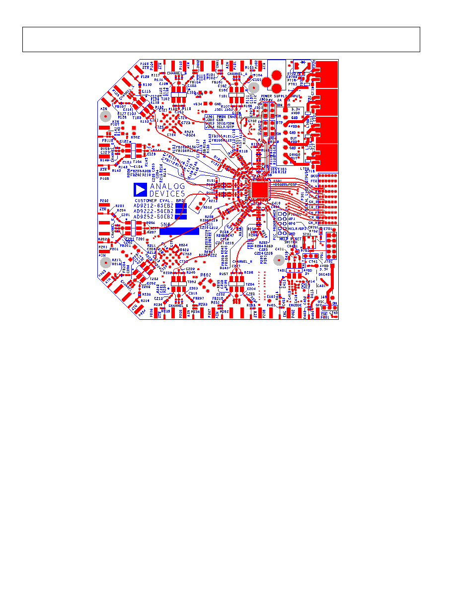
AD9222
Rev. 0 | Page 46 of 56
05
96
7-
0
79
Figure 74. Evaluation Board Layout, Primary Side
AD9222
Rev. 0 | Page 47 of 56
05
96
7-
0
80
Figure 75. Evaluation Board Layout, Ground Plane
AD9222
Rev. 0 | Page 48 of 56
05
96
7-
08
1
Figure 76. Evaluation Board Layout, Power Plane
AD9222
Rev. 0 | Page 49 of 56
05
96
7-
0
82
Figure 77. Evaluation Board Layout, Secondary Side (Mirrored Image)
AD9222
Rev. 0 | Page 50 of 56
Table 16. Evaluation Board Bill of Materials (BOM)
1
Item
Qnty.
per
Board REFDES
Device
Pkg.
Value
Mfg.
Mfg.
Part
Number
1 1 AD9222-50EBZ PCB
PCB
PCB
2 118 C101, C102, C107,
C108, C109, C114,
C115, C116, C121,
C122, C123, C128,
C201, C202, C207,
C208, C209, C214,
C215, C216, C221,
C222, C223, C228,
C301, C302, C304,
C305, C306, C401,
C402, C403, C409,
C410, C411, C412,
C413, C414, C415,
C416, C417, C418,
C501, C504, C505,
C506, C508, C509,
C511, C513, C518,
C519, C522, C523,
C524, C525, C528,
C529, C530, C532,
C534, C536, C537,
C538, C601, C604,
C605, C606, C608,
C609, C611, C613,
C616, C617, C618,
C619, C622, C623,
C624, C625, C628,
C629, C630, C632,
C634, C636, C701,
C702, C703, C706,
C708, C710, C712,
C723, C724, C725,
C726, C727, C730,
C731, C732, C733,
C734, C735, C740,
C741, C742, C743,
C744, C745, C746,
C747, C748, C749,
C750, C751, C752,
C753
Capacitor 402 0.1 F, ceramic, X5R,
10 V, 10% tol
Murata GRM155R71C104KA88D
3 8 C104, C111, C118,
C125, C204, C211,
C218, C225
Capacitor 402 2.2 pF, ceramic, COG,
0.25 pF tol, 50 V
Murata GRM1555C1H2R20CZ01D
4 8 C510, C512, C533,
C535, C610, C612,
C633, C635
Capacitor 805 10 F, 6.3 V ±10%
ceramic, X5R
Murata GRM219R60J106KE19D
5 1 C303
Capacitor 603
4.7 F, ceramic, X5R,
6.3 V, 10% tol
Murata GRM188R60J475KE19D
6 4 C507, C531, C607,
C631
Capacitor 402 1000 pF, ceramic, X7R,
25 V, 10% tol
Murata GRM155R71H102KA01D
7 8 C502, C515, C521,
C527, C602, C615,
C621, C627
Capacitor 402 0.018 F, ceramic, X7R,
16 V, 10% tol
AVX 0402YC183KAT2A
AD9222
Rev. 0 | Page 51 of 56
Item
Qnty.
per
Board REFDES
Device
Pkg.
Value
Mfg.
Mfg.
Part
Number
8 8 C503, C514, C520,
C526, C603, C614,
C620, C626
Capacitor 402 22 pF, ceramic, NPO,
5% tol, 50 V
Murata GRM1555C1H220JZ01D
9 1 C704
Capacitor 1206 10 F, tantalum,
16 V, 20% tol
Rohm TCA1C106M8R
10 9
C307, C714, C715,
C716, C717, C719,
C720, C721, C722
Capacitor 603 1 F, ceramic, X5R,
6.3 V, 10% tol
Murata GRM188R61C105KA93D
11 16 C540, C541, C544,
C545, C548, C549,
C552, C553, C640,
C641, C644, C645,
C648, C649, C652,
C653
Capacitor 805 0.1 F, ceramic, X7R,
50 V, 10% tol
Murata GRM21BR71H104KA01L
12 4
C705, C707, C709,
C711
Capacitor 603 10 F, ceramic, X5R,
6.3 V, 20% tol
Murata GRM188R60J106ME47D
13 1
CR401
Diode
SOT-23 30 V, 20 mA, dual
Schottky
Agilent
Technologies
HSMS-2812-TR1G
14
2
CR701, CR702
LED
603
Green, 4 V, 5 m candela
Panasonic
LNJ314G8TRA
15
1
D702
Diode
DO-214AB
3 A, 30 V, SMC
Micro
Commercial Co.
SK33-TP
16
1
D701
Diode
DO-214AA
5 A, 50 V, SMC
Micro
Commercial Co.
S2A-TP
17 1
F701
Fuse
1210
6.0 V, 2.2 A trip-current
resettable fuse
Tyco/Raychem NANOSMDC110F-2
18 1
FER701
Choke
coil 2020
10 H, 5 A, 50 V, 190
@ 100 MHz
Murata DLW5BSN191SQ2L
19 24 FB101, FB102,
FB103, FB104,
FB105, FB106,
FB107, FB108,
FB109, FB110,
FB111, FB112,
FB201, FB202,
FB203, FB204,
FB205, FB206,
FB207, FB208,
FB209, FB210,
FB211, FB212
Ferrite bead
603
10 , test frequency
100 MHz, 25% tol,
500 mA
Murata BLM18BA100SN1D
20 4
JP501, JP502,
JP601, JP602
Connector 2-pin 100 mil header jumper,
2-pin
Samtec TSW-102-07-G-S
21 6
J301, J302, J303,
J304, J401, J701
Connector 3-pin 100 mil header jumper,
3-pin
Samtec TSW-103-07-G-S
23 1
J702
Connector 10-pin 100 mil header, male,
2 × 5 double row
straight
Samtec TSW-105-08-G-D
24 8
L701, L702, L703,
L704, L705, L706,
L707, L708
Ferrite bead
1210
10 H, bead core 3.2 ×
2.5 × 1.6 SMD, 2 A
Murata BLM31PG500SN1L
25 8
L501, L502, L503,
L504, L601, L602,
L603, L604
Inductor 402 120 nH, test freq
100 MHz, 5% tol,
150 mA
Murata LQG15HNR12J02D
AD9222
Rev. 0 | Page 52 of 56
Item
Qnty.
per
Board REFDES
Device
Pkg.
Value
Mfg.
Mfg.
Part
Number
26 20 L505, L506, L507,
L508, L509, L510,
L511, L512, L513,
L514, L515, L516,
L517, L518, L519,
L520, L605, L606,
L607, L608, L609,
L610, L611, L612,
L613, L614, L615,
L616, L617, L618,
L619, L620
Resistor
805
0 , 1/8 W, 5% tol
NIC
Components
Corp.
NRC04Z0TRF
27 1
OSC401
Oscillator
SMT
Clock oscillator,
50.00 MHz, 3.3 V,
±5% duty cycle
Valphey Fisher
VFAC3H-L-50MHz
28 9
P101, P103, P105,
P107, P201, P203,
P205, P207, P401
Connector SMA Side-mount SMA for
0.063" board thickness
Johnson
Components
142-0701-851
29 1
P301
Connector HEADER 1469169-1, right angle
2-pair, 25 mm, header
assembly
Tyco 6469169-1
30 1
P701
Connector 0.1",
PCMT
RAPC722, power
supply connector
Switchcraft RAPC722X
31 21 R301, R307, R401,
R402, R410, R413,
R504, R505, R511,
R512, R523, R524,
R604, R605, R611,
R612, R623, R624,
R711, R714, R715
Resistor 402 10 k, 1/16 W,
5% tol
NIC
Components
Corp.
NRC04J103TRF
32 18 R103, R117, R129,
R142, R203, R219,
R235, R253, R317,
R405, R415, R416,
R417, R418, R706,
R707, R708, R709
Resistor 402 0 , 1/16 W,
5% tol
NIC
Components
Corp.
NRC04Z0TRF
33 8
R102, R115, R128,
R141, R202, R218,
R234, R252
Resistor 402 64.9 , 1/16 W,
1% tol
NIC
Components
Corp.
NRC04F64R9TRF
34 8
R104, R116, R130,
R143, R204, R220,
R236, R254
Resistor 603 0 , 1/10 W,
5% tol
NIC
Components
Corp.
NRC06Z0TRF
35 28 R109, R111, R112,
R123, R125, R126,
R135, R138, R139,
R148, R149, R150,
R211, R212, R214,
R228, R231, R232,
R246, R249, R250,
R262, R265, R266,
R319, R710, R712,
R713
Resistor 402 1 k, 1/16 W,
1% tol
NIC
Components
Corp.
NRC04F1001TRF
36 16 R108, R110, R121,
R122, R134, R136,
R146, R147, R209,
R210, R226, R227,
R242, R245, R260,
R261
Resistor 402 33 , 1/16 W,
5% tol
NIC
Components
Corp.
NRC04J330TRF
AD9222
Rev. 0 | Page 53 of 56
Item
Qnty.
per
Board REFDES
Device
Pkg.
Value
Mfg.
Mfg.
Part
Number
37 8
R161, R162, R163,
R164, R208, R225,
R241, R259
Resistor 402 499 , 1/16 W,
1% tol
NIC
Components
Corp.
NRC04F4990TRF
38 3
R303,
R305,
R306
Resistor
402
100 k, 1/16 W,
1% tol
NIC
Components
Corp.
NRC04F1003TRF
39 1
R414
Resistor
402
4.12 k, 1/16W,
1% tol
NIC
Components
Corp.
NRC04F4121TRF
40 1
R404
Resistor
402
49.9 , 1/16 W,
0.5% tol
Susumu RR0510R-49R9-D
41 1
R309
Resistor
402
4.99 k, 1/16 W,
5% tol
NIC
Components
Corp.
NRC04F4991TRF
42 2
R310, R501, R535,
R601, R634
Potentiometer 3-lead
10 k, Cermet trimmer
potentiometer, 18 turn
top adjust, 10%, 1/2 W
COPAL
ELECTRONICS
CT94EW103
43 1
R308
Resistor
402
470 k, 1/16 W,
5% tol
NIC
Components
Corp.
NRC04J474TRF
44 4
R502, R536, R602,
R635
Resistor 402 39 k, 1/16 W,
5% tol
NIC
Components
Corp.
NRC04J393TRF
45 16 R513, R514, R518,
R519, R525, R526,
R530, R531, R613,
R614, R618, R619,
R625, R626, R630,
R631
Resistor 402 187 , 1/16 W,
1% tol
NIC
Components
Corp.
NRC04F1870TRF
46 8
R515, R520, R527,
R532, R615, R620,
R627, R632
Resistor 402 374 , 1/16 W,
1% tol
NIC
Components
Corp.
NRC04F3740TRF
47 8
R503, R507, R508,
R509, R603, R607,
R608, R609
Resistor 402 274 , 1/16 W,
1% tol
NIC
Components
Corp.
NRC04F2740TRF
48 11 R425,R427, R429,
R431, R433, R435,
R436, R439, R441,
R443, R445
Resistor 201 0 , 1/20 W,
5% tol
NIC
Components
Corp.
NRC02Z0TRF
49 4
R701
Resistor
402
4.7 k, 1/16 W,
1% tol
NIC
Components
Corp.
NRC04J472TRF
50 1
R702
Resistor
402
261 , 1/16 W,
1% tol
NIC
Components
Corp.
NRC04F2610TRF
51 1
R716
Resistor
603
261 , 1/16 W,
1% tol
NIC
Components
Corp.
NRC06F261OTRF
52 2
R420,
R421
Resistor
402
240 , 1/16 W,
5% tol
NIC
Components
Corp.
NRC04J241TRF
53 2
R422,
R423
Resistor
402
100 , 1/16 W,
1% tol
NIC
Components
Corp.
NRC04F1000TRF
54 1
S701
Switch
SMD
LIGHT TOUCH,
100GE, 5 mm
Panasonic EVQ-PLDA15
AD9222
Rev. 0 | Page 54 of 56
Item
Qnty.
per
Board REFDES
Device
Pkg.
Value
Mfg.
Mfg.
Part
Number
55 9
T101, T102, T103,
T104, T201, T202,
T203, T204, T401
Transformer CD542 ADT1-1WT+,
1:1 impedance ratio
transformer
Mini-Circuits ADT1-1WT+
56 2
U704,
U707
IC
SOT-223 ADP33339AKC-1.8-RL,
1.5 A, 1.8 V LDO
regulator
Analog Devices
ADP3339AKCZ-1.8-RL
57 2
U501,
U601
IC
CP-64-3 AD8334ACPZ-REEL,
ultralow noise
precision dual VGA
Analog Devices
AD8334ACPZ-REEL
58 1
U706
IC
SOT-223 ADP33339AKC-5-RL7 Analog
Devices
ADP3339AKCZ-5-RL7
59 1
U705
IC
SOT-223 ADP33339AKC-3.3-RL Analog
Devices
ADP3339AKCZ-3.3-RL
60 1
U301
IC
CP-64-3 AD9222BCPZ-50, octal,
12-bit, 50 MSPS serial
LVDS 1.8 V ADC
Analog Devices
AD9222BCPZ-50
61 1
U302
IC
SOT-23 ADR510ARTZ, 1.0 V,
precision low noise
shunt voltage
reference
Analog Devices
ADR510ARTZ
62 1
U401
IC
LFCSP
CP-32-2
AD9515BCPZ, 1.6 GHz
clock distribution IC
Analog Devices
AD9515BCPZ
63 1
U702
IC
SC70,
MAA06A
NC7WZ07P6X_NL,
UHS dual buffer
Fairchild NC7WZ07P6X_NL
64 1
U703
IC
SC70,
MAA06A
NC7WZ16P6X_NL,
UHS dual buffer
Fairchild NC7WZ16P6X_NL
65 1
U701
IC
8-SOIC Flash prog
mem 1kx14,
RAM size 64 × 8,
20 MHz speed, PIC12F
controller series
Microchip PIC12F629-I/SNG
1
This BOM is RoHS compliant.
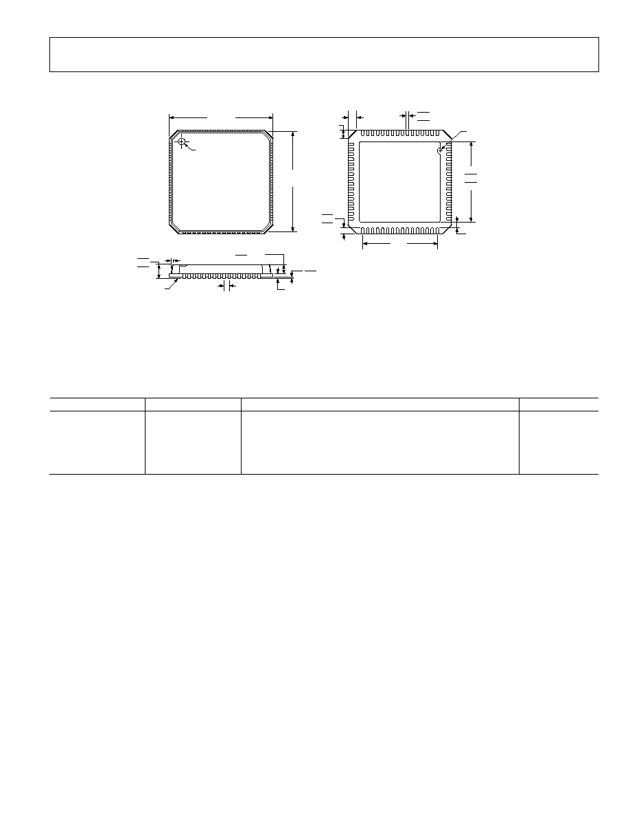
AD9222
Rev. 0 | Page 55 of 56
OUTLINE DIMENSIONS
0.25 MIN
COMPLIANT TO JEDEC STANDARDS MO-220-VMMD-4
PIN 1
INDICATOR
TOP
VIEW
8.75
BSC SQ
9.00
BSC SQ
1
64
16
17
49
48
32
33
0.45
0.40
0.35
0.50 BSC
0.20 REF
12° MAX
0.80 MAX
0.65 TYP
1.00
0.85
0.80
7.50
REF
0.05 MAX
0.02 NOM
0.60 MAX
0.60 MAX
EXPOSED PAD
(BOTTOM VIEW)
0.30
0.25
0.18
SEATING
PLANE
PIN 1
INDICATOR
7.25
7.10 SQ
6.95
12
21
05
-
0
Figure 78. 64-Lead Lead Frame Chip Scale Package [LFCSP_VQ]
9 mm × 9 mm Body, Very Thin Octal
(CP-64-3)
Dimensions shown in millimeters
ORDERING GUIDE
Model
Temperature Range
Package Description
Package Option
AD9222BCPZ-40
1
-40°C to +85°C
64-Lead Lead Frame Chip Scale Package [LFCSP_VQ]
CP-64-3
AD9222BCPZRL7-40
1
-40°C to +85°C
64-Lead Lead Frame Chip Scale Package [LFCSP_VQ] Tape and Reel
CP-64-3
AD9222BCPZ-50
1
-40°C to +85°C
64-Lead Lead Frame Chip Scale Package [LFCSP_VQ]
CP-64-3
AD9222BCPZRL7-50
1
-40°C to +85°C
64-Lead Lead Frame Chip Scale Package [LFCSP_VQ] Tape and Reel
CP-64-3
AD9222-50EBZ
Evaluation
Board
1
Z = Pb-free part.

AD9222
Rev. 0 | Page 56 of 56
NOTES
©2006 Analog Devices, Inc. All rights reserved. Trademarks and
registered trademarks are the property of their respective owners.
D05967-0-9/06(0)
Document Outline
- þÿ
- þÿ
- þÿ
- þÿ
- þÿ
- þÿ
- þÿ
- þÿ
- þÿ
- þÿ
- þÿ
- þÿ
- þÿ
- þÿ
- þÿ
- þÿ
- þÿ
- Power Dissipation and Power-Down Mode
- þÿ
- þÿ
- þÿ
- þÿ
- þÿ
- þÿ
- þÿ
- External Reference Operation
- þÿ
- þÿ
- þÿ
- RESERVED LOCATIONS
- þÿ
- þÿ
- þÿ
- Exposed Paddle Thermal Heat Slug Recommendations
- þÿ
- þÿ