 | ÐлекÑÑоннÑй компоненÑ: AD9229 | СкаÑаÑÑ:  PDF PDF  ZIP ZIP |
Äîêóìåíòàöèÿ è îïèñàíèÿ www.docs.chipfind.ru
Quad 12-Bit, 50/65 MSPS
Serial LVDS 3V A/D Converter
Preliminary Technical Data
AD9229
FEATURES
·
Four ADCs in one package
·
Serial LVDS digital output data rates (ANSI-644)
·
Data clock output provided
·
On Chip Reference and SHA
·
SNR = 70 dB at Fin up to Nyquist
·
Excellent Linearity:
-
DNL =
±
0.3 LSB (Typical)
-
INL =
±
0.6 LSB (Typical)
·
500 MHz full power analog bandwidth
·
Per Channel Core Power Dissipation = 270mW at 65MSPS /
200mW at 50MSPS
·
1 Vpp 2 Vpp input voltage range
·
+3.0 V supply operation
·
Power down mode
APPLICATIONS
·
Digital beam forming systems in ultrasound
·
Wireless and wired broadband communications
·
Communications test equipment
·
Radar and satellite imaging sub-systems
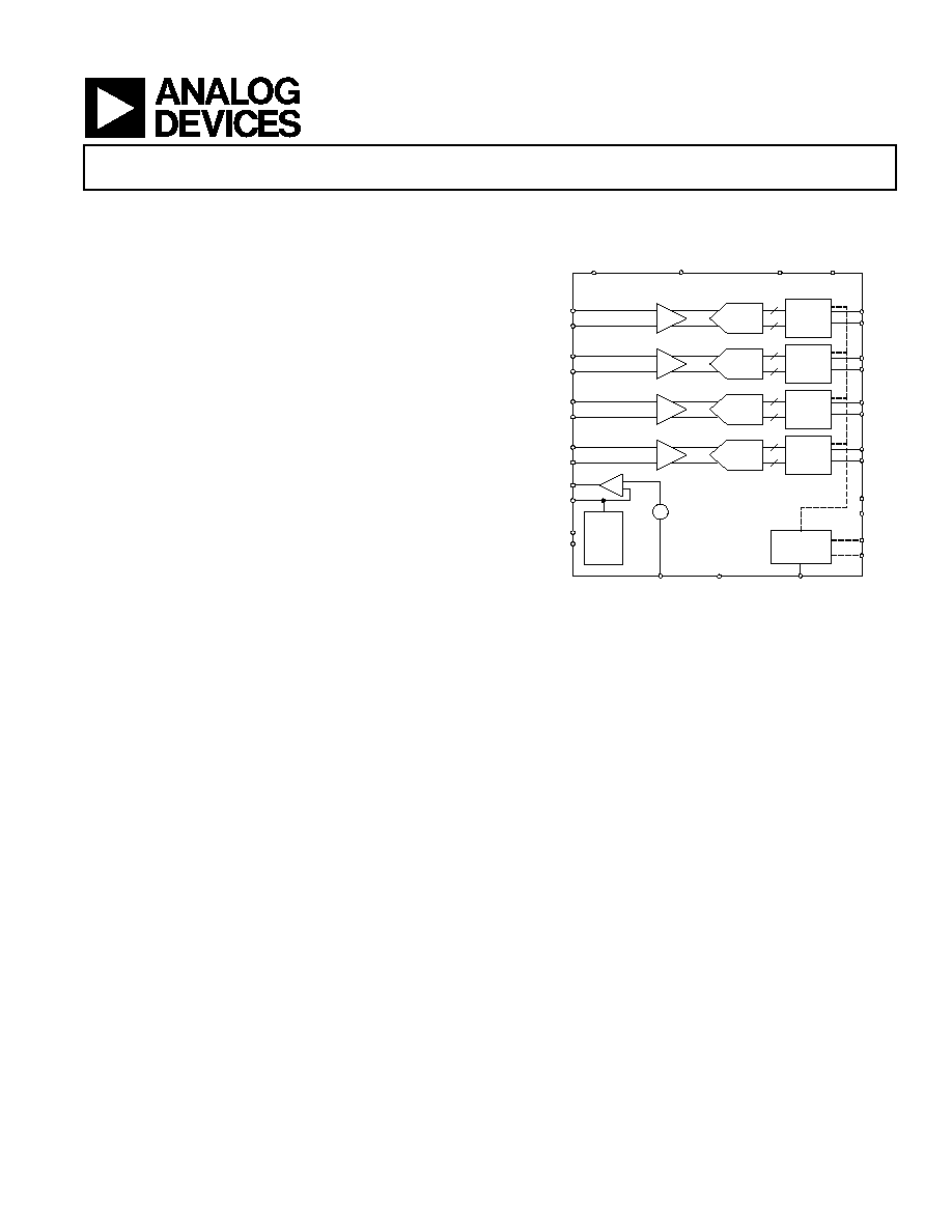
FUNCTIONAL BLOCK DIAGRAM
Serial
LVDS
Pipeline
ADC
SHA
Data Rate
Multiplier
Ref
Select
+
-
0.5 V
Serial
LVDS
Pipeline
ADC
SHA
Serial
LVDS
Pipeline
ADC
SHA
Serial
LVDS
Pipeline
ADC
SHA
AD9229
D1+A
D1-A
LVDSBIAS
AGND
VREF
SENSE
VIN+A
VIN-A
VIN+B
VIN-B
VIN+C
VIN-C
VIN+D
VIN-D
AVDD
DRVDD
12
12
12
12
PDWN
DCO+
DCO-
REFT
REFB
CLK
D1+B
D1-B
D1+C
D1-C
D1+D
D1-D
DRGND
DCO+
DCO-
FCO+
FCO-
Figure 1. Functional Block Diagram
PRODUCT DESCRIPTION
The AD9229 is a quad 12-bit monolithic sampling analogto
digital converter with an onchip trackandhold circuit and is
designed for low cost, low power, small size and ease of use. The
product operates up to a 65 MSPS conversion rate and is optimized
for outstanding dynamic performance where a small package size is
critical.
The ADC requires a single+3.0 V power supply and a TTL/CMOS
compatible sample rate clock for full performance operation. No
external reference or driver components are required for many
applications. A separate output power supply pin supports LVDS
compatible serial digital output levels.
The ADC automatically multiplies up the sample rate clock for the
appropriate LVDS serial data rate. An MSB trigger is provided to
signal a new output byte. Power down is supported and consumes
less than 3mW when enabled.
Fabricated on an advanced CMOS process, the AD9229 is available
in a 48-LFCSP package specified over the industrial temperature
range (40°C to +85°C).
PRODUCT HIGHLIGHTS
1. Four analog-to-digital converters are contained in one small,
space saving package.
2. A Data Clock Output (DCO) is provided which operates up to
390 MHz.
3. The outputs of each ADC are serialized with a maximum data
output rate of 780 Mbps (12-bits x 65 MSPS).
4. The AD9229 operates from a single +3.0 V analog power
supply.
Rev. PrF 10/06/2003
Information furnished by Analog Devices is believed to be accurate and reliable.
However, no responsibility is assumed by Analog Devices for its use, nor for any
infringements of patents or other rights of third parties that may result from its
use. No license is granted by implication or otherwise under any patent or patent
rights of Analog Devices. Trademarks and registered trademarks are the property
of their respective companies.
One Technology Way, P.O. Box 9106, Norwood, MA 02062-9106, U.S.A.
Tel: 781.329.4700
www.analog.com
Fax: 781.326.8703
© 2003 Analog Devices, Inc. All rights reserved.

AD9229
Preliminary Technical Data
Rev. PrF | Page 2 of 15
Oct. 6, 2003
TABLE OF CONTENTS
AD9229--Specifications ........................................................................ 3
DIGITAL SPECIFICATIONS ........................................................... 4
AC SPECIFICATIONS....................................................................... 4
SWITCHING SPECIFICATIONS.................................................... 5
EXPLANATION OF TEST LEVELS................................................ 5
Absolute Maximum Ratings .................................................................. 6
EQuivalent circuits.................................................................................. 7
TYPICAL PERFORMANCE CHARACTERISTICS ......................... 8
Theory of Operation.............................................................................11
Analog Inputs ....................................................................................11
Voltage Reference..............................................................................11
Digital Outputs..................................................................................11
Timing ................................................................................................11
PLL ......................................................................................................11
Pin Function Descriptions ...................................................................12
Pin Configurations ................................................................................13
Timing Diagram ....................................................................................14
Ordering Guide .................................................................................15
REVISION HISTORY
Revision PrA: Initial Version
Revision PrB: Added Definition and Theory of Operation sections, updated Pin Configurations
Revision PrC: Deleted demux outputs
Revision PrD: Added Pin Info, Package Info
Revision PrE: Ch. 3.3V to 3.0V for supply, Updated Sinad spec typo, Added analog typical Cin, Overange Recovery Time, Latency
Revision PrF: Added 50MSPS Grade, Removed Clk-, Updated Power, SNR,LVDS Rset, Tpd Estimates, Added Equiv Ckts, Added FFT, VREF
figure, Corrected FCO, DCO polarity timing
Preliminary Technical Data
AD9229
Rev. PrF | Page 3 of 15
Oct. 6, 2003
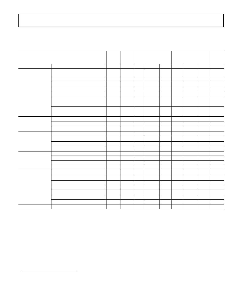
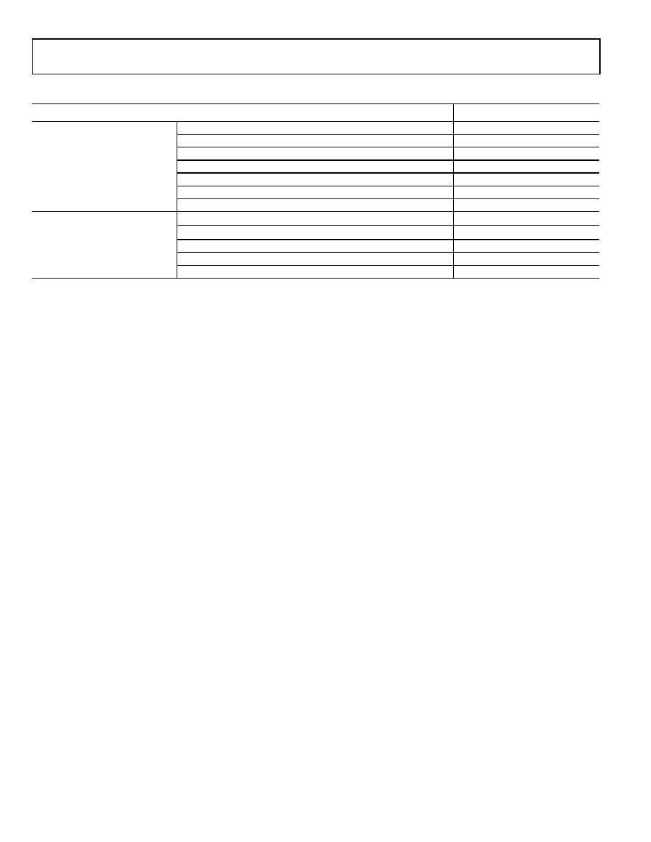
AD9229--SPECIFICATIONS
1
AVDD =
3.0
V, DRVDD =
3.0
V; INTERNAL REFERENCE; DIFFERENTIAL ANALOG INPUTS,MAXIMUM SAMPLE RATE,T
MIN
TO
T
MAX
, UNLESS OTHERWISE NOTED
Parameter
Temp
Test
Level
AD9229BCP-50
Min Typ Max
AD9229BCP-65
Min Typ Max
Unit
RESOLUTION
12
12
Bits
No Missing Codes
Full
VI
Guaran
teed
Guaran
teed
Offset Error
25
°
C
I
±
0.5
±
0.5
mV
Gain Error
25
°
C
I
±
0.5
±
0.5
%FS
Offset Matching
25
°
C
I
mV
Gain Matching
2
25
°
C
I
% FS
Differential Nonlinearity (DNL)
25
°
C
I
±
0.3
±
0.3
LSB
Full
VI
LSB
Integral Nonlinearity (INL)
25
°
C
I
±
0.6
±
0.6
LSB
ACCURACY
Full
VI
LSB
Offset Error
Full
V
ppm/
°
C
Gain Error
2
Full
V
ppm/
°
C
TEMPERATURE
DRIFT
Reference
Full
V
ppm/
°
C
Internal Reference Voltage
25
°
C
I
0.5
0.5
V
Output Current
Full
V
uA
Input Current
Full
V
uA
REFERENCE
Input Resistance
Full
V
k
Differential Input Voltage Range
1 2
1 2
Vpp
Common Mode Voltage
Full
V
1.5
1.5
V
Input Capacitance
Full
V
7
7
pF
ANALOG INPUTS
Analog Bandwidth, Full Power
Full
V
500
500
MHz
AVDD
Full
IV
2.7
3.0
3.6
2.7
3.0
3.6
V
DRVDD
Full
IV
2.7
3.0
3.6
2.7
3.0
3.6
V
Power Dissipation
3
Full
VI
940
1250
mW
Power Down Dissipation
Full
VI
<3
<3
mW
Power Supply Rejection Ratio (PSRR)
25
°
C
I
mV/V
IAVDD
3
Full
VI
268
367
mA
POWER SUPPLY
IDRVDD
3
Full
VI
28
30
mA
IPLLVDD
3
Full
VI
18
19
Table 1: DC Specifications
1
Specifications subject to change without notice
2
Gain error and gain temperature coefficients are based on the ADC only (with a fixed 0.5 V external reference and a 1 V p-p differential analog input).
3
Power dissipation measured with rated encode and a dc analog input (Outputs Static, I
VDD
= 0.). I
VCC
and I
VDD
measured with TBD MHz analog input @ 0.5dBFS.
AD9229
Preliminary Technical Data
Rev. PrF | Page 4 of 15
Oct. 6, 2003
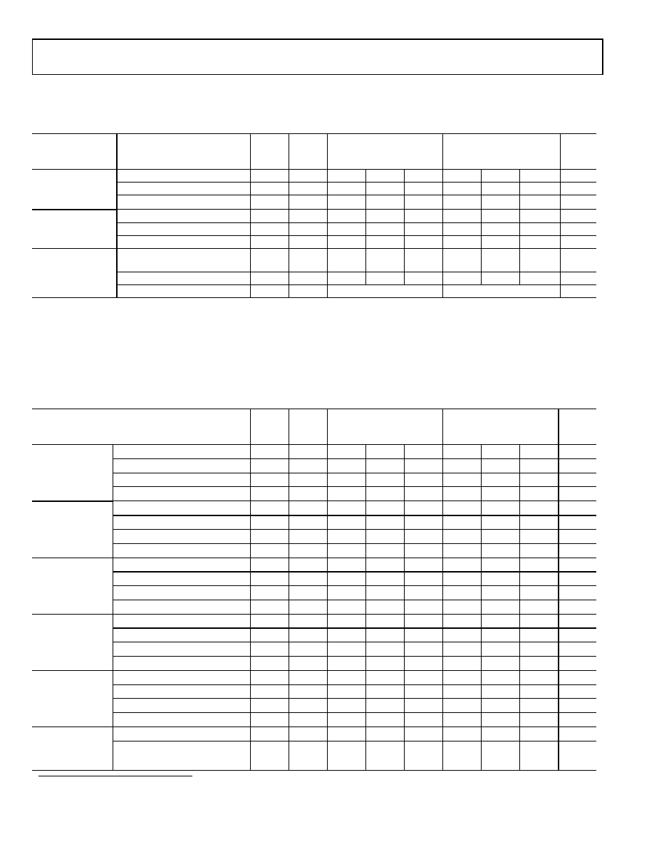
DIGITAL SPECIFICATIONS
AVDD =
3.0
V, DRVDD =
3.0
V
Parameter
Temp
Test
Level
AD9229BCP-50
Min Typ Max
AD9229BCP-65
Min Typ Max
Unit
V
IH
Full
IV
2.0
2.0
V
V
IL
Full
IV
0.8
0.8
V
CLOCK INPUT
Input Capacitance
25
°
C
IV
2
2
pF
Logic `1' Voltage
Full
IV
2.0
2.0
V
Logic `0' Voltage
Full
IV
0.8
0.8
V
PDWN INPUT
Input Capacitance
Full
IV
2
2
PF
Differential Output Voltage
(V
OD
)
Full
IV
247
454
247
454
mV
Output Offset Voltage (V
OS
)
Full
IV
1.125
1.375
1.125
1.375
V
DIGITAL OUTPUTS
(LVDS Mode)*
Output Coding
Full
IV
Offset Binary
Offset Binary
Table 2: Digital Specifications
*
LVDS Rset resistor = 3.6K, LVDS Output Termination Resistor= 100 Ohms.
AC SPECIFICATIONS
1
AVDD =
3.0
V, DRVDD =
3.0
V; INTERNAL REFERENCE; DIFFERENTIAL ANALOG INPUTS,MAXIMUM SAMPLE RATE,T
MIN
TO
T
MAX
, UNLESS OTHERWISE NOTED
Parameter
Temp
Test
Level
AD9229BCP-50
Min Typ Max
AD9229BCP-65
Min Typ Max
Unit
f
IN
= 10.3 MHz
25
°
C
V
70.5
70.5
dB
f
IN
= 19.6 MHz
25
°
C
V
dB
f
IN
= 32.5 MHz
25
°
C
I
69.7
69.7
dB
SIGNAL TO NOISE
RATIO (SNR)
Without
Harmonics
f
IN
= 51 MHz
25
°
C
V
dB
f
IN
= 10.3 MHz
25
°
C
V
70.3
70.3
dB
f
IN
= 19.6 MHz
25
°
C
V
dB
f
IN
= 32.5 MHz
25
°
C
I
69.5
69.5
dB
SIGNAL TO NOISE
RATIO (SINAD)
With Harmonics
f
IN
= 51 MHz
25
°
C
V
dB
f
IN
= 10.3 MHz
25
°
C
V
Bits
f
IN
= 19.6 MHz
25
°
C
V
Bits
f
IN
= 32.5 MHz
25
°
C
I
Bits
EFFECTIVE
NUMBER OF BITS
(ENOB)
f
IN
= 51 MHz
25
°
C
V
Bits
f
IN
= 10.3 MHz
25
°
C
V
dB
f
IN
= 19.6 MHz
25
°
C
V
85
85
dB
f
IN
= 32.5 MHz
25
°
C
I
dB
SPURIOUS FREE
DYNAMIC RANGE
(SFDR)
f
IN
= 51 MHz
25
°
C
V
dB
f
IN
= 10.3 MHz
25
°
C
V
dBc
f
IN
= 19.6 MHz
25
°
C
V
-85
-85
dBc
f
IN
= 32.5 MHz
25
°
C
I
dBc
SECOND AND
THIRD
HARMONIC
DISTORTION
f
IN
= 51 MHz
25
°
C
V
dBc
f
IN1
= 19 MHz, f
IN2
= 20 MHz
25
°
C
V
-85
-85
dBc
TWO TONE
INTERMOD
DISTORTION
(IMD)
f
IN1
= xx MHz, f
IN2
= xx MHz
25
°
C
V
dBc
1
SNR/harmonics based on an analog input voltage of 0.5 dBFS referenced to a 1 Vpp full-scale input range.
Preliminary Technical Data
AD9229
Rev. PrF | Page 5 of 15
Oct. 6, 2003
Parameter
Temp
Test
Level
AD9229BCP-50
Min Typ Max
AD9229BCP-65
Min Typ Max
Unit
CROSSTALK
Full
V
-80
-80
dB
Table 3: AC Specifications
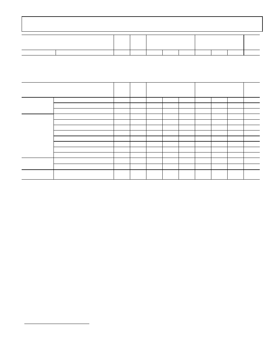
SWITCHING SPECIFICATIONS
AVDD = 3.0 V, DRVDD = 3.0 V; DIFFERENTIAL ENCODE INPUT
Parameter
Temp
Test
Level
AD9229BCP-50
Min Typ Max
AD9229BCP-65
Min Typ Max
Unit
Clock Rate
Full
VI
10
50
10
65
MSPS
Clock Pulse Width High (t
EH
)
Full
IV
ns
CLOCK
Clock Pulse Width Low (t
EL
)
Full
IV
ns
Valid Time (t
V
)
1
Full
VI
ns
Propagation Delay (t
PD
)
1
Full
VI
5
5
ns
MSB Propagation Delay (t
MSB
)
1
Full
VI
5
5
ns
Rise Time (t
R
) (20% to 80%)
Full
V
ns
Fall Time (t
F
) (20% to 80%)
Full
V
ns
DCO Propagation Delay (t
CPD
)
Full
VI
5
5
ns
Data to DCO Skew (t
PD
t
CPD
)
Full
IV
ns
OUTPUT
PARAMETERS IN
LVDS MODE
Pipeline Latency
Full
VI
9
9
cycles
Aperture Delay (t
A
)
25
°
C
V
ps
APERTURE
Aperture Uncertainty (Jitter)
25
°
C
V
<1
<1
ps rms
Out of Range
Recovery Time
Full
IV
2
2
cycles
Table 4: Switching Specifications
EXPLANATION OF TEST LEVELS
TEST LEVEL
I
100% production tested.
II
100% production tested at +25
°
C and guaranteed by design and characterization at specified temperatures.
III
Sample tested only.
IV
Parameter is guaranteed by design and characterization testing.
V
Parameter is a typical value only.
VI
100% production tested at +25
°
C and guaranteed by design and characterization for industrial temperature range.
1
t
V
and
t
PD
are measured from the transition points of the CLK input to the 50%/50% levels of the digital outputs swing. The digital output load during test is
not to exceed an ac load of 5 pF or a dc current of ±40 µA. Rise and fall times measured from 20% to 80%.
AD9229
Preliminary Technical Data
Rev. PrF | Page 6 of 15
Oct. 6, 2003
ABSOLUTE MAXIMUM RATINGS
Parameter
Rating
AVDD Voltage
3.9V
DRVDD Voltage
3.9V
Analog Input Voltage
Analog Input Current
Digital Input Voltage
Digital Output Current
Electrical
VREF Input Voltage
Operating Temperature Range (Ambient)
-40
°
C to +85
°
C
Maximum Junction Temperature
150
°
C
Lead Temperature (Soldering, 10 sec)
Maximum Case Temperature
Environmental
Storage Temperature Range (Ambient)
Table 5: Absolute Maximum Ratings
Stresses above those listed under the Absolute Maximum Ratings may cause permanent damage to the device. This is a stress rating only;
functional operation of the device at these or any other conditions above those indicated in the operational section of this specification is not
implied. Exposure to absolute maximum rating conditions for extended periods may affect device reliability.
Preliminary Technical Data
AD9229
Rev. PrF | Page 7 of 15
Oct. 6, 2003
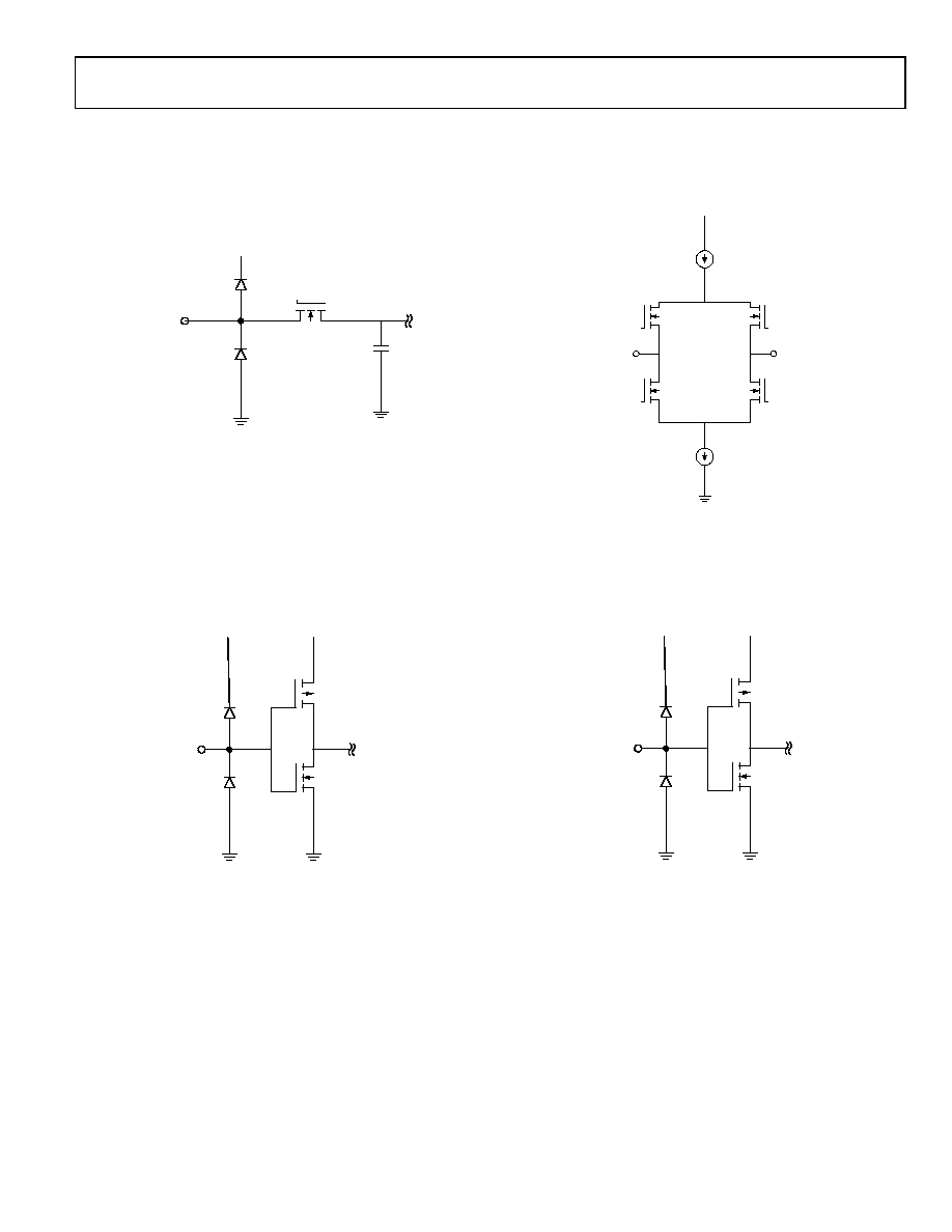
EQUIVALENT CIRCUITS
AVDD
ANALOG IN
Figure 2 Analog Inputs
CLK
AVDD
AVDD
Figure 3 Clock Input
DRVDD
V+
V+
V-
V-
DATAOUT+,
DCO+,FCO+
DATAOUT-,
DCO-,FCO-
3.5
M
A
3.5
M
A
Figure 4 LVDS Outputs
PDWN
AVDD
AVDD
Figure 5 PDWN Input
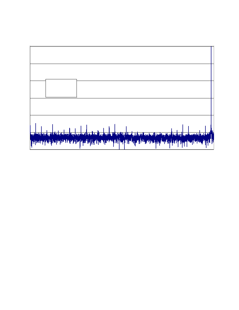
TYPICAL PERFORMANCE CHARACTERISTICS
-120
-100
-80
-60
-40
-20
0
0
5
10
15
20
25
30
MHz
dB
SNR = 68.7 dB
SINAD = 68.5 dB
SFDR = 88.6 dB
Measured FFT Performance 32MHz Ain at 65MSPS

Preliminary Technical Data
AD9229
Rev. PrF | Page 9 of 15
Oct. 6, 2003
Definitions
ANALOG BANDWIDTH
The analog input frequency at which the spectral power of the
fundamental frequency (as determined by the FFT analysis) is
reduced by 3 dB.
APERTURE DELAY
The delay between the 50% point of the rising edge of the
ENCODE command and the instant at which the analog input is
sampled.
APERTURE UNCERTAINTY (JITTER)
The sample-to-sample variation in aperture delay.
CROSSTALK
Coupling onto one channel being driven by a low level (-40 dBFS)
signal when the adjacent interfering channel is driven by a full-
scale signal.
DIFFERENTIAL ANALOG INPUT RESISTANCE,
DIFFERENTIAL ANALOG INPUT CAPACITANCE, AND
DIFFERENTIAL ANALOG INPUT IMPEDANCE
The real and complex impedances measured at each analog input
port. The resistance is measured statically and the capacitance and
differential input impedances are measured with a network
analyzer.
DIFFERENTIAL ANALOG INPUT VOLTAGE RANGE
The peak to peak differential voltage that must be applied to the
converter to generate a full scale response. Peak differential voltage
is computed by observing the voltage on a single pin and
subtracting the voltage from the other pin, which is 180 degrees out
of phase. Peak to peak differential is computed by rotating the
inputs phase 180 degrees and taking the peak measurement again.
Then the difference is computed between both peak measurements.
DIFFERENTIAL NONLINEARITY
The deviation of any code width from an ideal 1 LSB step.
EFFECTIVE NUMBER OF BITS
The effective number of bits (ENOB) is calculated from the
measured SNR based on the equation:
02
.
6
76
.
1
dB
SNR
ENOB
MEASURED
-
=
ENCODE PULSE WIDTH/DUTY CYCLE
Pulse width high is the minimum amount of time that the
ENCODE pulse should be left in logic "1" state to achieve rated
performance; pulse width low is the minimum time ENCODE
pulse should be left in low state. See timing implications of
changing tENCH in text. At a give clock rate, these specs define an
acceptable Encode duty cycle.
FULL SCALE INPUT POWER
Expressed in dBm. Computed using the following equation:
=
001
.
log
10
2
Input
Fullscale
Fullscale
Z
V
Power
rms
GAIN ERROR
Gain error is the difference between the measured and ideal full
scale input voltage range of the worst ADC.
GAIN MATCHING
Expressed in %FSR. Computed using the following equation:
%
100
*
2
min
max
min
max
+
-
=
FSR
FSR
FSR
FSR
ng
GainMatchi
where FSR
max
is the most positive gain error of the ADCs and
FSR
min
is the most negative gain error of the ADCs.
HARMONIC DISTORTION, SECOND
The ratio of the rms signal amplitude to the rms value of the
second harmonic component, reported in dBc.
HARMONIC DISTORTION, THIRD
The ratio of the rms signal amplitude to the rms value of the third
harmonic component, reported in dBc.
INTEGRAL NONLINEARITY
The deviation of the transfer function from a reference line
measured in fractions of 1 LSB using a "best straight line"
determined by a least square curve fit.

AD9229
Preliminary Technical Data
Rev. PrF | Page 10 of 15
Oct. 6, 2003
MINIMUM CONVERSION RATE
The encode rate at which the SNR of the lowest analog signal
frequency drops by no more than 3 dB below the guaranteed limit.
MAXIMUM CONVERSION RATE
The encode rate at which parametric testing is performed.
OFFSET ERROR
Offset error is the difference between the measured and ideal
voltage at the analog input that produces the midscale code at the
outputs. Offset error is given for the worst ADC.
OFFSET MATCHING
Expressed in mV. Computed using the following equation:
min
max
OFF
OFF
hing
OffsetMatc
-
=
where OFF
max
is the most positive offset error and OFF
min
is the
most negative offset error.
OUTPUT PROPAGATION DELAY
The delay between a differential crossing of CLK+ and CLK- and
the time when all output data bits are within valid logic levels.
NOISE (FOR ANY RANGE WITHIN THE ADC)
-
-
=
10
10
*
001
.
*
dBFS
dBc
dBm
Signal
SNR
FS
noise
Z
V
Where Z is the input impedance, FS is the full scale of the device
for the frequency in question, SNR is the value for the particular
input level and Signal is the signal level within the ADC reported in
dB below full scale. This value includes both thermal and
quantization noise.
POWER SUPPLY REJECTION RATIO
The ratio of a change in input offset voltage to a change in power
supply voltage.
SIGNAL-TO-NOISE-AND-DISTORTION (SINAD)
The ratio of the rms signal amplitude (set 1 dB below full scale) to
the rms value of the sum of all other spectral components,
including harmonics but excluding dc.
SIGNAL-TO-NOISE RATIO (WITHOUT HARMONICS)
The ratio of the rms signal amplitude (set at 1 dB below full scale)
to the rms value of the sum of all other spectral components,
excluding the first five harmonics and dc.
SPURIOUS-FREE DYNAMIC RANGE (SFDR)
The ratio of the rms signal amplitude to the rms value of the peak
spurious spectral component. The peak spurious component may
or may not be a harmonic. It also may be reported in dBc (i.e.,
degrades as signal level is lowered) or dBFS (i.e., always related back
to converter full scale).
TWO-TONE INTERMODULATION DISTORTION
REJECTION
The ratio of the rms value of either input tone to the rms value of
the worst third order intermodulation product; reported in dBc.
TWO-TONE SFDR
The ratio of the rms value of either input tone to the rms value of
the peak spurious component. The peak spurious component may
or may not be an IMD product. It also may be reported in dBc (i.e.,
degrades as signal level is lowered) or in dBFS (i.e., always relates
back to converter full scale).
WORST OTHER SPUR
The ratio of the rms signal amplitude to the rms value of the worst
spurious component (excluding the second and third harmonic)
reported in dBc.
TRANSIENT RESPONSE TIME
Transient response time is defined as the time it takes for the ADC
to reacquire the analog input after a transient from 10% above
negative full scale to 10% below positive full scale.
OUT-OF-RANGE RECOVERY TIME
Out of range recovery time is the time it takes for the ADC to
reacquire the analog input after a transient from 10% above positive
full scale to 10% above negative full scale, or from 10% below
negative full scale to 10% below positive full scale.
Preliminary Technical Data
AD9229
Rev. PrF | Page 11 of 15
Oct. 6, 2003
THEORY OF OPERATION
Analog Inputs
For best dynamic performance, the source impedances driving
VIN+ and VIN should be matched such that common-mode
settling errors are symmetrical. These errors will be reduced by the
common-mode rejection of the A/D.
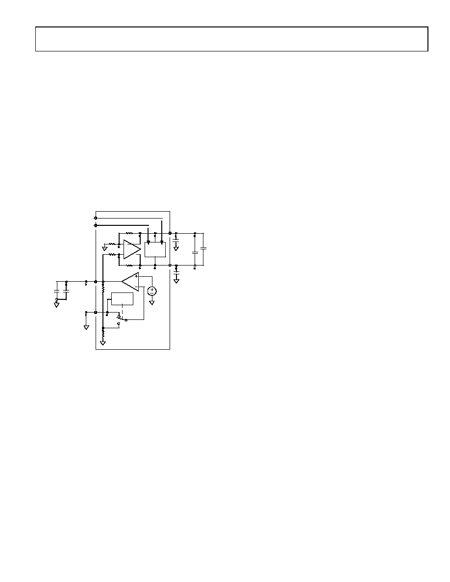
Voltage Reference
The AD9229 has a stable and accurate reference voltage on chip,
which sets the full-scale voltage at the analog input channels.
Internal reference mode is established by grounding the SENSE pin.
(Recommended decoupling capacitors shown below) The internal
reference can be bypassed by setting SENSE to AVDD and driving
VREF with an external 1V reference.
SENSE
ADC
CORE
SELECT
LOGIC
AD9229
VREF
VINB
VINA
REFB
REFT
0.1
u
F
10
uF
0.1
uF
10
uF
0.1
uF
0.1
uF
0.5V
Internal Reference Mode Connection
Digital Outputs
The AD9229's differential outputs conform to the ANSI-644 LVDS
standard. To set the LVDS bias current, place a resistor (RSET is
nominally equal to 3.6 k
) to ground at the LVDSBIAS pin. The
RSET resistor current (~ 1.2/RSET) is ratioed on-chip setting the
output current at each output equal to a nominal 3.5 mA. A 100
differential termination resistor placed at the LVDS receiver inputs
results in a nominal 350 mV swing at the receiver.
The AD9229's LVDS outputs facilitate interfacing with LVDS
receivers in custom ASICs and FPGAs that have LVDS capability
for superior switching performance in noisy environments. Single
point-to-point net topologies are recommended with a 100
termination resistor as close to the receiver as possible. It is
recommended to keep the trace length no longer than 12 inches
and to keep differential output trace lengths as equal as possible.
The format of the output data is offset binary.
Timing
Data from each A/D is serialized and provided on a separate
channel.
Two output clocks are provided to assist in capturing data from the
AD9229. The data clock out (DCO) is used to clock the output
data and is equal to 6 times the sample clock frequency. ( 390MHz
for 65MHz input clock) Data is clocked out of the AD9229 on the
rising and falling edges of DCO. The FCO clock signals the start of
a new serial word, the rising edge of FCO occurs at the start of an
MSB.
PLL
The AD9229 contains an internal PLL that is used to generate
internal clocking signals, if the PLL is unlocked, the data outputs
are static.
AD9229
Preliminary Technical Data
Rev. PrF | Page 12 of 15
Oct. 6, 2003
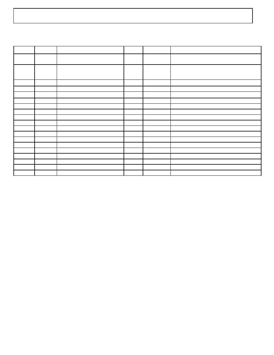
PIN FUNCTION DESCRIPTIONS
Pin No.
Name
Description
Pin No.
Name
Description
8,16,21,
29
AVDD
3.0
V Analog Supply
44
D+A
ADC A True Digital Output
9,12,15,
22,25,28,
31
AGND
Analog Ground
43
D-A
ADC A Complement Digital Output
2,35
DRVDD
3.0
V Digital Output Supply
42
D+B
ADC B True Digital Output
1,36
DRGND
Digital Ground
41
D-B
ADC B Complement Digital Output
32
PLLVDD
PLL
3.0
V Supply
40
D+C
ADC C True Digital Output
33
PLLGND
PLL Ground
39
D-C
ADC C Complement Digital Output
30
CLK
Input Clock
38
D+D
ADC D True Digital Output
18
VREF
Voltage Reference Input/Output
37
D1-D
ADC D Complement Digital Output
17
SENSE
Reference Mode Selection
48
DCO+
Data Clock Output True
20
REFT
Differential Reference (Positive)
47
DCO-
Data Clock Output Complement
19
REFB
Differential Reference (Negative)
46
FCO+
Frame Clock Indicator True Output
10
VIN+A
ADC A Analog Input True
45
FCO-
Frame Clock Indicator Complement Output
11
VIN-A
ADC A Analog Input Complement
34
LVDSBIAS
LVDS Output Current Set Resistor Pin
14
VIN+B
ADC B Analog Input True
7
PDWN
Power Down Selection ( Logic `1' = Power Down )
13
VIN-B
ADC B Analog Input Complement
3,4,5,6
DNC
Do Not Connect
23
VIN+C
ADC C Analog Input True
24
VIN-C
ADC C Analog Input Complement
27
VIN+D
ADC D Analog Input True
26
VIN-D
ADC D Analog Input Complement
Table 6: Pin Function Descriptions

Preliminary Technical Data
AD9229
Rev. PrF | Page 13 of 15
Oct. 6, 2003
PIN CONFIGURATIONS
1
12
13
24
25
36
37
48
DRGND
DRVDD
DNC
DNC
DNC
DNC
PDWN
AVDD
AGND
VIN+A
VIN-A
AGND
DRGND
DRVDD
LVDSBIAS
PLLGND
PLLVDD
AGND
CLK
AVDD
AGND
VIN+D
VIN-D
AGND
V
I
N
-
B
V
I
N
+
B
A
G
N
D
A
V
D
D
S
E
N
S
E
V
R
E
F
R
E
F
B
R
E
F
T
A
V
D
D
A
G
N
D
V
I
N
+
C
V
I
N
-
C
D
C
O
+
D
C
O
-
F
C
O
+
F
C
O
-
D
+
A
D
-
A
D
+
B
D
-
B
D
+
C
D
-
C
D
+
D
D
-
D
AD9229
AD9229
Preliminary Technical Data
Rev. PrF | Page 14 of 15
Oct. 6, 2003
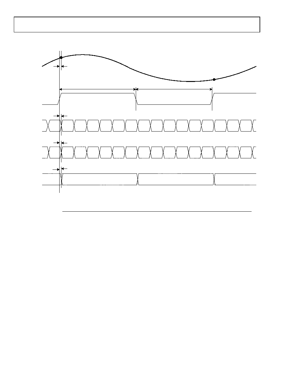
TIMING DIAGRAM
MSB
LSB
Data
Out
DCO+
MSB
AIN
DCO-
CLK
LSB
D10
D9
D8
D7
D6
D5
D4
D3
D2
D1
N-1
N
t
A
t
EH
t
EL
t
PD
t
CPD
FCO-
FCO+
t
FPD
Figure 6: Serial LVDS Outputs
NOTE : Latency = 9 cycles
Preliminary Technical Data
AD9229
Rev. PrF | Page 15 of 15
Oct. 6, 2003
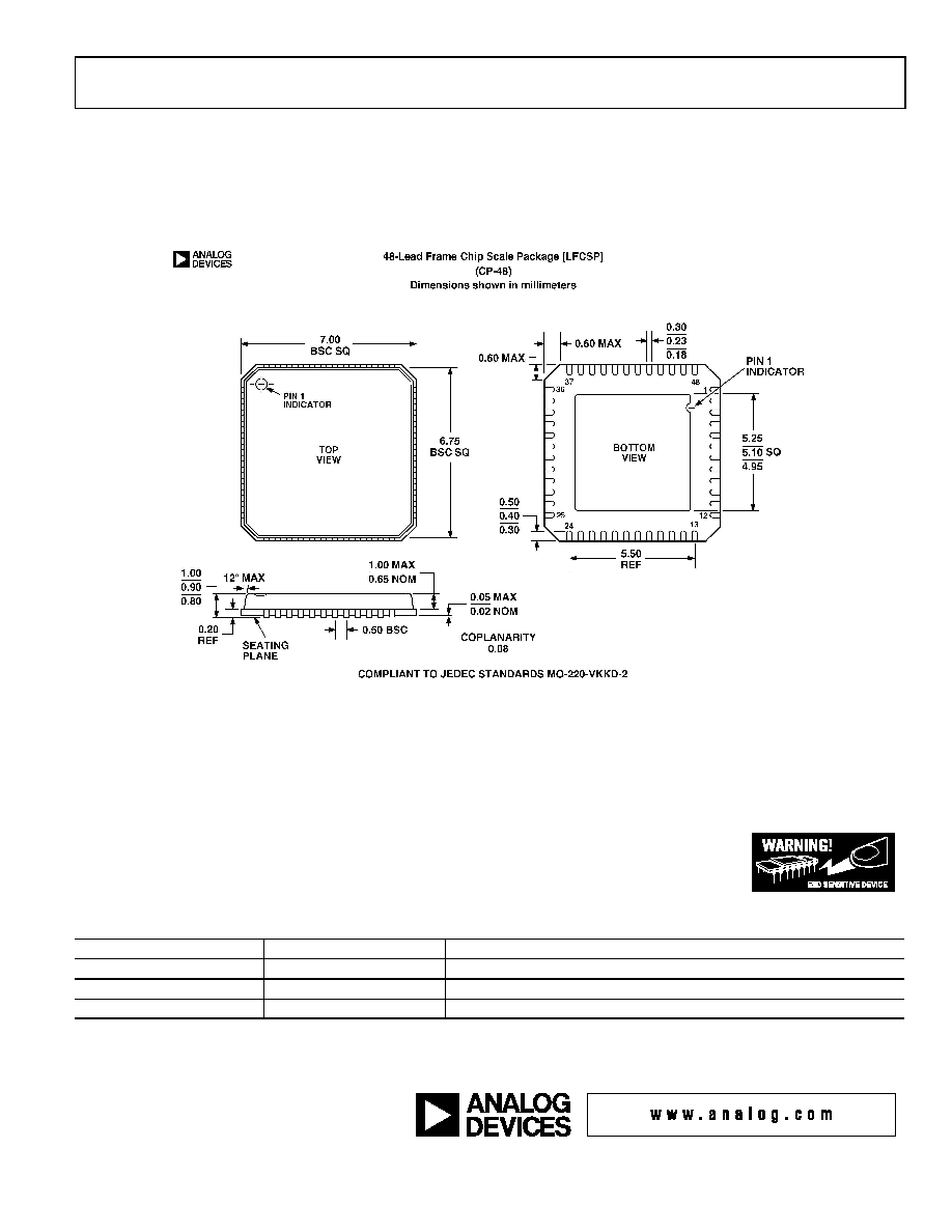
OUTLINE DIMENSIONS
Figure 7
ESD CAUTION
ESD (electrostatic discharge) sensitive device. Electrostatic charges as high as 4000 V readily accumulate on the
human body and test equipment and can discharge without detection. Although this product features proprietary
ESD protection circuitry, permanent damage may occur on devices subjected to high energy electrostatic discharges.
Therefore, proper ESD precautions are recommended to avoid performance degradation or loss of functionality.
Ordering Guide
Model
Temperature Range
Description
AD9229BCP-50
-40
°
C to +85
°
C (Ambient)
48-LFCSP
AD9229BCP-65
-40
°
C to +85
°
C (Ambient)
48-LFCSP
AD9229/PCB
25°C (Ambient)
Evaluation Board ( Supplied with 65 Grade )
Table 7: Ordering Guide
© 2002 Analog Devices, Inc. All rights reserved. Trademarks and
registered trademarks are the property of their respective companies.
Printed in the U.S.A.
C02959-0-11/02(0)