 | ÐлекÑÑоннÑй компоненÑ: AD9233 | СкаÑаÑÑ:  PDF PDF  ZIP ZIP |
AD9233, 12-Bit, 105/125 MSPS, 1.8 V ADC Preliminary Data Sheet (Rev. PrG)
12-Bit, 105/125 MSPS, 1.8 V ADC
Preliminary Technical Data
AD9233
Rev. PrG
Information furnished by Analog Devices is believed to be accurate and reliable.
However, no responsibility is assumed by Analog Devices for its use, nor for any
infringements of patents or other rights of third parties that may result from its use.
Specifications subject to change without notice. No license is granted by implication
or otherwise under any patent or patent rights of Analog Devices. Trademarks and
registered trademarks are the property of their respective owners.
One Technology Way, P.O. Box 9106, Norwood, MA 02062-9106, U.S.A.
Tel: 781.329.4700
www.analog.com
Fax: 781.461.3113
©2005 Analog Devices, Inc. All rights reserved.
FEATURES
1.8 V analog supply operation
1.8 V to 3.3 V output supply
SNR = 69.3 dBc (69.8dBFS) to Nyquist
SFDR = 85 dBc to Nyquist
Low power: 395 mW
Differential input with 650 MHz bandwidth
On-chip reference and sample-and-hold
DNL = ±0.13 LSB
Flexible analog input: 1 V p-p to 2 V p-p range
Offset binary or twos complement data format
Clock duty cycle stabilizer
APPLICATIONS
Ultrasound equipment
IF sampling in communications receivers:
IS-95, CDMA-One, IMT-2000
Battery-powered instruments
Hand-held scopemeters
Low cost digital oscilloscopes
GENERAL DESCRIPTION
The AD9233 is a monolithic, single 1.8 V analog supply, 12-bit,
125 MSPS analog-to-digital converter (ADC), featuring a high
performance sample-and-hold amplifier (SHA) and voltage
reference. The AD9233 uses a multistage differential pipelined
architecture with output error correction logic to provide 12-bit
accuracy at 125 MSPS data rates and guarantees no missing
codes over the full operating temperature range.
The wide bandwidth, truly differential SHA allows a variety of
user-selectable input ranges and offsets including single-ended
applications. It is suitable for multiplexed systems that switch
full-scale voltage levels in successive channels and for sampling
single-channel inputs at frequencies well beyond the Nyquist rate.
Combined with power and cost savings over previously available
ADCs, the AD9233 is suitable for applications in communications,
imaging, and medical ultrasound. A differential clock input is used
to control all internal conversion cycles. A duty cycle stabilizer
(DCS) compensates for wide variations in the clock duty cycle
while maintaining excellent overall ADC performance. The digital
output data is presented in straight binary or twos complement
formats. A differential data output clock (DCO) is provided to
ensure proper latch timing with receiving logic.
FUNCTIONAL BLOCK DIAGRAM
DRVDD
AVDD
AGND
0.5V
CLK+
PWDN DrGND
OTR
VIN+
VIN
REFT
REFB
AD9233
VREF
SENSE
SHA
A/D
MDAC1
4
8
13
1
A/D
8-STAGE
1 1/2-BIT PIPELINE
REF
SELECT
CLOCK
DUTY CYCLE
STABILIZER
MODE
SELECT
CORRECTION LOGIC
OUTPUT BUFFERS
D11 (MSB)
D0 (LSB)
SPI SCLK/DFS
SPI CSB
SPI SDIO/DCS
DCO
CLK-
Figure 1.
Fabricated on an advanced CMOS process, the AD9233 is avail-
able in a 48- lead LFCSP and is specified over the industrial
temperature range (-40°C to +85°C).
PRODUCT DESCRIPTIONS
1. The AD9233 operates from a single analog 1.8 V power
supply and features a separate digital output driver supply
to accommodate 1.6 - 3.3 V logic families.
2. The patented SHA input maintains excellent performance
for input frequencies up to 180 MHz and can be config-
ured for single-ended or differential operation.
3. The clock DCS maintains overall ADC performance over a
wide range of clock pulse widths.
4. Standard serial port interface supports various product
features and functions, such as data formatting (offset bi-
nary, 2's complement, or Gray coding), enabling a clock
duty cycle stabilizer, power-down, and voltage reference
mode.

AD9233
Preliminary Technical Data
Rev. PrG | Page 2 of 19
TABLE OF CONTENTS
DC Specifications ............................................................................. 3
AC Specifications.............................................................................. 4
Digital Specifications........................................................................ 5
Switching Specifications .................................................................. 6
Explanation of Test Levels...... Error! Bookmark not defined.
Absolute Maximum Ratings............................................................ 6
ESD Caution.................................................................................. 6
Terminology ...................................................................................... 7
Pin Configuration and Function Descriptions............................. 8
Theory of Operation ........................................................................ 9
Analog Input and Reference Overview ......................................9
Clock Input Considerations...................................................... 10
Power Dissipation and Standby Mode .................................... 11
Digital Outputs ........................................................................... 12
Timing ......................................................................................... 12
Voltage Reference ....................................................................... 13
Operational Mode Selection .. Error! Bookmark not defined.
Evaluation Board ..................... Error! Bookmark not defined.
Outline Dimensions ....................................................................... 19
Ordering Guide .......................................................................... 19
REVISION HISTORY
6/05--Revision PrG: Preliminary Version
Preliminary Technical Data
AD9233
Rev. PrG | Page 3 of 19
DC SPECIFICATIONS
AVDD = 1.8 V, DRVDD = 3.3 V, sample rate = 125 MSPS, 2 V p-p differential input, 1.0 V internal reference, unless otherwise noted.
Table 1.
AD9233BCPZ-105 AD9233BCPZ-125
Parameter Temp
Min Typ Max
Min Typ Max
Unit
RESOLUTION Full
12
12
Bits
ACCURACY
No Missing Codes
Full
Guaranteed
Guaranteed
Offset Error
Full
±0.25
±
±0.25
±
% FSR
Gain Error (External 1.0 V Reference)
25°C
±0.2
±0.2
%
FSR
Gain Error
Full
±0.3
±0.3
%
FSR
Differential Nonlinearity (DNL)
1
Full
±TBD
±TBD
LSB
25°C
±0.13
±0.13
LSB
Integral Nonlinearity (INL)
1
Full
±
±
LSB
25°C
±0.5
±0.5
LSB
TEMPERATURE DRIFT
Offset Error
Full
TBD
TBD
ppm/°C
Gain Error
Full
TBD
TBD
ppm/°C
Gain Error (External 1.0 V Reference)
Full
TBD
TBD
ppm/°C
INTERNAL VOLTAGE REFERENCE
Output Voltage Error (1 V Mode)
Full
TBD
TBD
mV
Load Regulation @ 1.0 mA
Full
TBD
TBD
mV
INPUT REFERRED NOISE
VREF = 1.0 V
25°C
TBD
TBD
LSB rms
ANALOG INPUT
Input Span, VREF = 1.0 V
Full
2
2
V
p-p
Input Capacitance
2
Full
8
8
pF
REFERENCE INPUT RESISTANCE
Full
TBD
TBD
k
POWER SUPPLIES
Supply Voltage
AVDD Full
1.7 1.8 1.9
1.7 1.8 1.9
V
DRVDD Full
1.6 3.3 3.6
1.6 3.3 3.6
V
Supply Current
IAVDD
1
Full
219
219
mA
IDRVDD
1
(3.3V) Full
17
17
mA
IDRVDD
1
(1.8V
Full
9
9
mA
PSRR Full
±0.01
±0.01
%
FSR
POWER CONSUMPTION
DC Input
Full
395
395
mW
Sine Wave Input
3
(DrVDD=1.8V)
Full
410
410
mW
Sine Wave Input
4
(DrVDD=3.3V)
Full
450
450
mW
Standby Power
Full
40
40
mW
Powerdown Power
5
Full
1.8
1.8
mW
1
Measured at the maximum clock rate, f
IN
= 2.4 MHz, full-scale sine wave, with approximately 5 pF loading on each output bit.
2
Input capacitance refers to the effective capacitance between one differential input pin and AGND. Refer to Figure 2 for the equivalent analog input structure.
3
Measured at ac specification conditions with approximately 5 pF loading on each output bit.
4
Measured at ac specification conditions with approximately 5 pF loading on each output bit.
5
Standby power is measured with a dc input, the CLK pin inactive (that is, set to AVDD or AGND).

AD9233
Preliminary Technical Data
Rev. PrG | Page 4 of 19
AC SPECIFICATIONS
AVDD = 1.8 V, DRVDD = 3.3 V, sample rate = 125 MSPS, 2 V p-p differential input, 1.0 V internal reference, AIN = -0.5 dBFS, DCS on,
unless otherwise noted.
Table 2.
AD9233BCPZ-105 AD9233BCPZ-125
Parameter Temp
Min Typ Max Min Typ Max
Unit
SIGNAL-TO-NOISE-RATIO
(SNR)
f
IN
= 2.4 MHz
25°C
69.5
69.5
dB
Full
69.0
69.0
dB
f
IN
= 70 MHz
25°C
69.3
69.3
dB
Full
68.8
68.8
dB
f
IN
= 100 MHz
25°C
69.2
69.2
dB
f
IN
= 180 MHz
25°C
68.0
68.0
dB
SIGNAL-TO-NOISE-AND DISTORTION (SINAD)
f
IN
= 2.4 MHz
25°C
69.2
69.2
dB
Full
68.7
68.7
dB
f
IN
= 70 MHz
25°C
69.0
69.0
dB
Full
68.5
68.5
dB
f
IN
= 100 MHz
25°C
67.9
67.9
dB
f
IN
= 180 MHz
25°C
67.7
67.7
dB
EFFECTIVE NUMBER OF BITS (ENOB)
f
IN
= 2.4 MHz
25°C
11.3
11.3
Bits
f
IN
= 70 MHz
25°C
11.2
11.2
Bits
f
IN
= 100 MHz
25°C
11.0
11.0
Bits
f
IN
= 180 MHz
25°C
11.0
11.0
Bits
WORST SECOND OR THIRD HARMONIC
f
IN
= 2.4 MHz
25°C
88
88
dBc
Full
82
82
dBc
f
IN
= 70 MHz
25°C
85
85
dBc
Full
82
82
dBc
f
IN
= 100 MHz
25°C
83
83
dBc
f
IN
= 180 MHz
25°C
80
80
dBc
SPURIOUS-FREE DYNAMIC RANGE (SFDR)
f
IN
= 2.4 MHz
25°C
88
88
dBc
Full
82
82
dBc
f
IN
= 70 MHz
25°C
85
85
dBc
Full
82
82
dBc
f
IN
= 100 MHz
25°C
83
83
dBc
f
IN
= 180 MHz
25°C
80
80
dBc
TWO TONE SFDR
f
IN
= 70 MHz, 71 MHz (-7 dBFS Each Tone)
25°C
dBFS
f
IN
= 70 MHz, 71 MHz (-7 dBFS Each Tone)
Full
dBFS
ANALOG INPUT BANDWIDTH
25°C
650
650
MHz
Preliminary Technical Data
AD9233
Rev. PrG | Page 5 of 19
DIGITAL SPECIFICATIONS
AVDD1 = 1.8V V, DRVDD = 3.3 V Unless otherwise noted
Table 3.
Parameter Temp
AD9233BCPZ-105
AD9233BCPZ-125
Unit
Min Typ Max Min Typ
Max
CMOS LOGIC INPUTS (SPI CSB ,
SPI SDIO / DFS, SPI SCLK / DCS,
CLKIN+, PWDN)
High Level Input Voltage
Full
2.0
2.0
V
Low Level Input Voltage
Full
0.8
0.8
V
High Level Input Current
Full
-10
+10
-10
+10
µA
Low Level Input Current
Full
-10
+10
-10
+10
µA
Input Capacitance
Full
2
2
pF
DIFFERENTIAL CLOCK INPUTS
Internal Common-Mode Bias
Full
1.2
1.2
V
Differential Input
(CLKIN+ - CLKIN-)
Full 0.2
6
0.2
6
Vp-p
Input Voltage Range
Full AVDD-0.3
AVDD+1.5
AVDD-0.3
AVDD+1.5
V
Input Common-Mode Range
Full 1.1V
AVDD 1.1V
AVDD V
Input Capacitance
Full
pF
Input Resistance
Full 8
10
12
8
10 12
DIGITAL OUTPUTS
DRVDD = 3.3 V
High Level Output Voltage
(IOH = 50 µA)
Full
3.29
3.29
V
High Level Output Voltage
(IOH = 0.5 mA)
Full
3.25
3.25
V
Low Level Output Voltage
(IOH = 1.6 mA)
Full
0.2
0.2
V
Low Level Output Voltage
(IOH = 50 µA)
Full
0.05
0.05
V
DRVDD = 1.8 V
High Level Output Voltage
(IOH = 50 µA)
Full
1.79
1.79
V
High Level Output Voltage
(IOH = 0.5 mA)
Full
1.75
1.75
V
Low Level Output Voltage
(IOH = 1.6 mA)
Full
0.2
0.2
V
Low Level Output Voltage
(IOH = 50 µA)
Full
0.05
0.05
V
AD9233
Preliminary Technical Data
Rev. PrG | Page 6 of 19
SWITCHING SPECIFICATIONS
AVDD = 3 V, DRVDD = 2.5 V, UNLESS OTHERWISE NOTED.
Table 4.
AD9233BCPZ-105 AD9233BCPZ-125
Parameter Temp
Min Typ Max Min Typ Max
Unit
CLOCK
INPUT
PARAMETERS
Maximum Conversion Rate
Full
105
125
MSPS
Minimum
Conversion
Rate Full
10
10
MSPS
CLK
Period
Full
9.5
8
ns
CLK Pulse Width High
1
Full TBD
TBD
ns
CLK Pulse Width Low
1
Full TBD
TBD
ns
DATA
OUTPUT
PARAMETERS
Output Propagation Delay (t
PD
)
2
Full
3.6
3.6
ns
Pipeline Delay (Latency)
Full
12
12
Cycles
Aperture Delay (t
A
)
Full
TBD
TBD
ns
Aperture Uncertainty (Jitter, t
J
)
Full
0.1
0.1
ps
rms
Wake-Up Time
3
Full
TBD
TBD
ms
OUT-OF-RANGE
RECOVERY
TIME
Full
TBD
TBD
Cycles
1
With duty cycle stabilizer (DCS) enabled.
2
Output propagation delay is measured from CLK 50% transition to DATA 50% transition, with 5 pF load.
3
Wake-up time is dependant on the value of the decoupling capacitors, typical values shown with 0.1 µF and 10 µF capacitors on REFT and REFB.
ABSOLUTE MAXIMUM RATINGS
Table 5.
Parameter With
Re-
spect to
Min Max Unit
ELECTRICAL
AVDD AGND
V
DRVDD DGND
V
AGND DGND
V
AVDD DRVDD
V
D0 to D13
DGND
V
CLK AGND
V
VIN+, VIN
AGND
V
VREF AGND
V
SENSE AGND
V
REFT, REFB
AGND
V
PDWN, SPI CSB, SPI
SDIO, SPI SCLK
AGND V
ENVIRONMENTAL
Storage Temperature
65
+125
°C
Operating Temperature Range
40
+85
°C
Lead Temperature Range
(Soldering 10 sec)
+300
°C
Junction Temperature
+150
°C
Stresses above those listed under Absolute Maximum Ratings
may cause permanent damage to the device. This is a stress rat-
ing only; functional operation of the device at these or any
other condition s above those indicated in the operational sec-
tion of this specification is not implied. Exposure to absolute
maximum rating conditions for extended periods may affect
device reliability.
Thermal Resistance
JA
is specified for the worst-case conditions on a 4-layer board
in still air, in accordance with EIA/JESD51-1.
Table 6. Thermal Resistance
Package Type
JA
JC
Unit
CP-48 32.5
TBD
°C/W
Airflow increases heat dissipation effectively reducing
JA
. Also,
more metal directly in contact with the package leads from
metal traces, through holes, ground, and power planes reduce
the
JA
. It is recommended that the exposed paddle be soldered
to the ground plane for the LFCSP package. There is an in-
creased reliability of the solder joints, and maximum thermal
capability of the package is achieved with the exposed paddle
soldered to the customer board.
ESD CAUTION
ESD (electrostatic discharge) sensitive device. Electrostatic charges as high as 4000 V readily accumulate on the
human body and test equipment and can discharge without detection. Although this product features proprie-
tary ESD protection circuitry, permanent damage may occur on devices subjected to high energy electrostatic
discharges. Therefore, proper ESD precautions are recommended to avoid performance degradation or loss of
functionality.

Preliminary Technical Data
AD9233
Rev. PrG | Page 7 of 19
TERMINOLOGY
Analog Bandwidth (Full Power Bandwidth)
The analog input frequency at which the spectral power of the
fundamental frequency (as determined by the FFT analysis) is
reduced by 3 dB.
Aperture Delay (t
A
)
The delay between the 50% point of the rising edge of the clock
and the instant at which the analog input is sampled.
Aperture Uncertainty (Jitter, t
J
)
The sample-to-sample variation in aperture delay.
Integral Nonlinearity (INL
)
The deviation of each individual code from a line drawn from
negative full scale through positive full scale. The point used as
negative full scale occurs ½ LSB before the first code transition.
Positive full scale is defined as a level 1½ LSB beyond the last
code transition. The deviation is measured from the middle of
each particular code to the true straight line.
Differential Nonlinearity (DNL, No Missing Codes)
An ideal ADC exhibits code transitions that are exactly 1 LSB
apart. DNL is the deviation from this ideal value. Guaranteed no
missing codes to 12-bit resolution indicates that all 4096 codes
must be present over all operating ranges.
Offset Error
The major carry transition should occur for an analog value
½ LSB below VIN+ = VIN. Offset error is defined as the
deviation of the actual transition from that point.
Gain Error
The first code transition should occur at an analog value ½ LSB
above negative full scale. The last transition should occur at an
analog value 1½ LSB below the positive full scale. Gain error is
the deviation of the actual difference between first and last code
transitions and the ideal difference between first and last code
transitions.
Temperature Drift
The temperature drift for offset error and gain error specifies
the maximum change from the initial (25°C) value to the value
at T
MIN
or T
MAX
.
Power Supply Rejection Ratio
The change in full scale from the value with the supply at the
minimum limit to the value with the supply at its maximum
limit.
Signal to Noise and Distortion (SINAD)
Error! Bookmark not defined.
The ratio of the rms input signal amplitude to the rms value of
the sum of all other spectral components below the Nyquist
frequency, including harmonics but excluding dc.
Effective Number of Bits (ENOB)
The effective number of bits for a sine wave input at a given
input frequency can be calculated directly from its measured
SINAD by
(
)
02
6
76
1
.
.
SINAD
ENOB
-
=
Signal to Noise Ratio (SNR)
Error! Bookmark not defined.
The ratio of the rms input signal amplitude to the rms value of
the sum of all other spectral components below the Nyquist
frequency, excluding the first six harmonics and dc.
Spurious-Free Dynamic Range (SFDR)
Error! Bookmark not defined.
The difference in dB between the rms input signal amplitude
and the peak spurious signal. The peak spurious component
may or may not be a harmonic.
Two Tone SFDR
Error! Bookmark not defined.
The ratio of the rms value of either input tone to the rms value
of the peak spurious component. The peak spurious component
may or may not be an IMD product.
Clock Pulse Width and Duty Cycle
Pulse width high is the minimum amount of time that the clock
pulse should be left in the Logic 1 state to achieve rated per-
formance. Pulse width low is the minimum time the clock pulse
should be left in the low state. At a given clock rate, these speci-
fications define an acceptable clock duty cycle.
Minimum Conversion Rate
The clock rate at which the SNR of the lowest analog signal fre-
quency drops by no more than 3 dB below the guaranteed limit.
Maximum Conversion Rate
The clock rate at which parametric testing is performed.
Output Propagation Delay (t
PD
)
The delay between the clock rising edge and the time when all
bits are within valid logic levels.
Out-of-Range Recovery Time
The time it takes for the ADC to reacquire the analog input
after a transition from 10% above positive full scale to 10%
above negative full scale, or from 10% below negative full scale
to 10% below positive full scale
AD9233
Preliminary Technical Data
Rev. PrG | Page 8 of 19
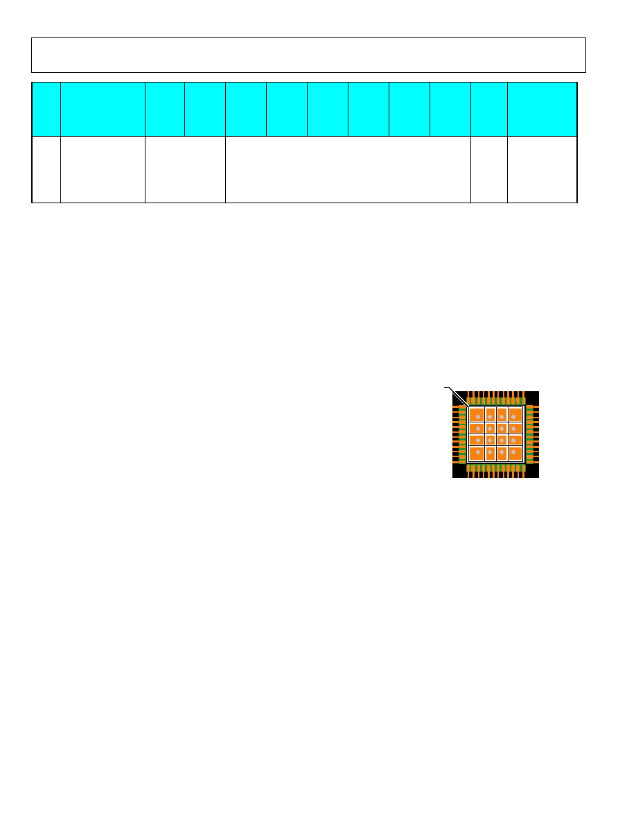
PIN CONFIGURATION AND FUNCTION DESCRIPTIONS
1
2
3
4
5
6
7
8
9
10
11
12
(LSB)D0
D1
D2
D3
D4
D5
DRGND
DRVDD
D6
D7
D8
D9
RBIAS
CML
AVDD
AGND
VIN
VIN+
AGND
REFT
REFB
VREF
SENSE
35
PWDN
36
34
33
32
31
30
29
28
27
26
25
AD9233
TOP VIEW
(Not to Scale)
Pin 0 (Exposed Paddle):AGND
PIN 1
INDICATOR
NC
NC
D1
0
(M
S
B
)
D
1
1
Figure 2. 48-Lead LFCSP
Table 7. Pin Function Description--48-Lead LFCSP
Pin No.
Mnemonic
Description
1 to 6, 9 to 14,
D0 (LSB) to D11 (MSB)
Data Output Bits.
45, 46
NC
No Connection
7, 16, 47
DRGND
Digital Output Ground.
8, 17, 48
DRVDD
Digital Output Driver Supply (1.8 V to 3.3 V).
15 OR
Out-of-Range
Indicator.
18 SPI
SDIO/DCS
Serial Port Interface Data Input/Output in Serial Port Mode; Duty Cycle Stabilizer
Select Pin in External Pin Mode.
19 SPI
SCLK/DFS
Serial Port Interface Clock in Serial Port Mode; Data Format Select Pin in External
Pin Mode.
20
SPI CSB
Serial Port Interface Chip Select (Active Low).
0, 21, 23, 29,
32, 37, 41
AGND
Analog Ground. (Pin 0 is the exposed thermal pad on bottom of package.)
22, 24, 33, 40, 42
AVDD
Analog Power Supply (Nominally 1.8 V).
25
SENSE
Reference Mode Selection(See Table 9 ).
26
VREF
Voltage Reference Input/Output.
27
REFB
Differential Reference (-).
28
REFT
Differential Reference (+).
30
VIN+
Analog Input Pin (+).
31
VIN
Analog Input Pin (-).
34
CML
Common-Mode Level Bias Output for Analog Inputs.
35 RBIAS
External Bias Resister Connection. A TBD k resister should be connected be-
tween
this pin and analog ground (GND).
36
PDWN
Power-Down Function Select.
38 CLKIN+
Clock
Input--True.
39 CLKIN
Clock
Input--Complement.
43
OE
Output Enable (Active Low).
44
DCO
Data Clock Output.
Pin 0 (Exposed Paddle):AGND
Preliminary Technical Data
AD9233
Rev. PrG | Page 9 of 19
THEORY OF OPERATION
The AD9233 architecture consists of a front-end sample and
hold amplifier (SHA) followed by a pipelined switched capaci-
tor ADC. The quantized outputs from each stage are combined
into a final 12-bit result in the digital correction logic. The pipe-
lined architecture permits the first stage to operate on a new
input sample, while the remaining stages operate on preceding
samples. Sampling occurs on the rising edge of the clock.
Each stage of the pipeline, excluding the last, consists of a low
resolution flash ADC connected to a switched capacitor DAC
and interstage residue amplifier (MDAC). The residue amplifier
magnifies the difference between the reconstructed DAC output
and the flash input for the next stage in the pipeline. One bit of
redundancy is used in each stage to facilitate digital correction
of flash errors. The last stage simply consists of a flash ADC.
The input stage contains a differential SHA that can be ac- or
dc-coupled in differential or single-ended modes. The output-
staging block aligns the data, carries out the error correction,
and passes the data to the output buffers. The output buffers are
powered from a separate supply, allowing adjustment of the
output voltage swing. During power-down, the output buffers
go into a high impedance state.
ANALOG INPUT AND REFERENCE OVERVIEW
The analog input to the AD9233 is a differential switched ca-
pacitor SHA that has been designed for optimum performance
while processing a differential input signal. An on-board com-
mon-mode voltage reference is included in the design and is
available from the CML pin. Optimum performance is
achieved when the common-mode voltage of the analog input is
set by the CML pin voltage (~0.55 × AVDD).
In Figure 3, the clock signal alternatively switches the SHA be-
tween sample mode and hold mode. When the SHA is switched
into sample mode, the signal source must be capable of charg-
ing the sample capacitors and settling within one-half of a clock
cycle. A small resistor in series with each input can help reduce
the peak transient current required from the output stage of the
driving source. Also, a small shunt capacitor can be placed
across the inputs to provide dynamic charging currents. This
passive network creates a low-pass filter at the ADC's input;
therefore, the precise values are dependant upon the application.
In IF undersampling applications, any shunt capacitors should
be reduced or removed. In combination with the driving source
impedance, they would limit the input bandwidth.
Figure 3.Switched-Capacitor SHA Input
For best dynamic performance, the source impedances driving
VIN+ and VIN should be matched such that common-mode
settling errors are symmetrical. These errors are reduced by the
common-mode rejection of the ADC.
An internal differential reference buffer creates positive and
negative reference voltages, REFT and REFB, that define the
span of the ADC core. The output common mode of the refer-
ence buffer is set to VCMREF (~1.6V), and the REFT and REFB
voltages and span are defined as:
REFT = VCMREF+½ VREF)
REFB = VCMREF-½ VREF
Span = 2 × (REFT - REFB) = 2 × VREF
It can be seen from the equations above that the REFT and
REFB voltages are symmetrical about the VCMREF voltage and,
by definition, the input span is twice the value of the VREF
voltage.
Differential Input Configurations
Optimum performance is achieved while driving the AD9233 in
a differential input configuration. For baseband applications, the
AD8138 differential driver provides excellent performance and
a flexible interface to the ADC. The output common-mode
voltage of the AD8138 is easily set to AVDD/2, and the driver
can be configured in a Sallen-Key filter topology to provide
band limiting of the input signal.
Figure 4. Differential Input Configuration Using the AD8138
AD9233
VIN+
VIN
CML
AVDD
1V p-p
49.9
523
0.1µF
33
33
20pF
499
499
499
AD8138
05491-004
AD9233
Preliminary Technical Data
Rev. PrG | Page 10 of 19
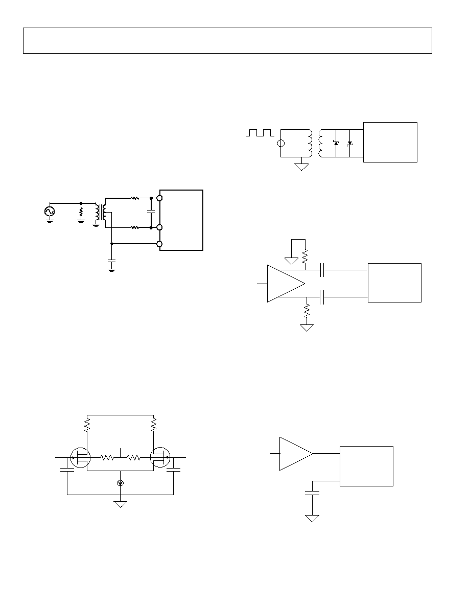
At input frequencies in the second Nyquist zone and above, the
performance of most amplifiers is not adequate to achieve the
true performance of the AD9233. This is especially true in IF
undersampling applications where frequencies in the 70 MHz to
100 MHz range are being sampled. For these applications, dif-
ferential transformer coupling is the recommended input con-
figuration. The value of the shunt capacitor is dependent on the
input frequency and source impedance and should be reduced
or removed. The CML voltage is connected to the center tap of
the transformer's secondary winding to bias the analog input.
An example is shown in Figure 5.
VIN
Figure 5. Differential Transformer-Coupled Configuration
The signal characteristics must be considered when selecting a
transformer. Most RF transformers saturate at frequencies be-
low a few MHz, and excessive signal power can also cause core
saturation, which leads to distortion.
CLOCK INPUT CONSIDERATIONS
For optimum performance, the AD9233 the sample clock inputs
(CLK+ and CLK-) should be clocked with a differential signal.
This signal is typically ac ac-coupled into the CLK+ and CLK-
pins via a transformer or capacitors. These pins are biased in-
ternally and require no additional bias(See Figure X).
1.2V
CLK+
CLK-
2pF
2pF
AVDD
Figure .Equivalent Clock Input Circuit
Figure X shows one preferred method for clocking the AD9233.
The clock source (low jitter) is converted from single-ended to
differential using an RF transformer. The back-to-back Schottky
diodes across the transformer secondary limit clock excursions
into the AD9233 to approximately 0.8 V p-p differential. This
helps prevent the large voltage swings of the clock from feeding
through to other portions of the AD9233 while preserving the
fast rise and fall times of the signal, which are critical to a low
jitter performance.
Clock
Source
CLK+
CLK-
AD9233
Figure X. Transformer Coupled Differential Clock
If a low jitter clock is available, another option is to ac-couple a
differential PECL signal to the sample clock input pins as shown
in Figure X. The AD9512 (or same family) from offers excellent
jitter performance.
CLK+
CLK-
AD9246
0.1uF
0.1uF
AD9512
PECL
150
150
Figure X. Differential PECL Sample Clock
In some applications it may acceptable to drive the sample clock
inputs with a single ended CMOS signal. In such applications,
CLK+ should be directly driven from a CMOS gate, while the
CLK- pin should be bypassed to ground with a 0.1uF capacitor
(see figure X). CLK+ may be directly driven from a CMOS gate.
While the CLK+ input circuit supply is AVDD (1.8V), this input
is designed to withstand input voltages up to 3.6V, making the
selection of the drive logic voltage very flexible.
CLK+
CLK-
AD9233
0.1uF
CMOS
Figure X. Differential PECL Sample Clock
AD9233
VIN+
VIN
33
33
10pF
49.9
CML
0.1µ
F
2V p-p
05491-005
Preliminary Technical Data
AD9233
Rev. PrG | Page 11 of 19
Clock Input Considerations
Typical high speed ADCs use both clock edges to generate a
variety of internal timing signals, and as a result may be sensi-
tive to clock duty cycle. Commonly, a 5% tolerance is required
on the clock duty cycle to maintain dynamic performance
characteristics. The AD9233 contains a DCS (duty cycle stabi-
lizer) that retimes the nonsampling edge, providing an internal
clock signal with a nominal 50% duty cycle. This allows a wide
range of clock input duty cycles without affecting the perform-
ance of the AD9233. Noise and distortion performance are
nearly flat for a wide range duty cycles with the DCS on. The
DCS
The duty cycle stabilizer uses a delay-locked loop (DLL) to
create the nonsampling edge. As a result, any changes to the
sampling frequency require approximately TBD clock cycles to
allow the DLL to acquire and lock to the new rate.
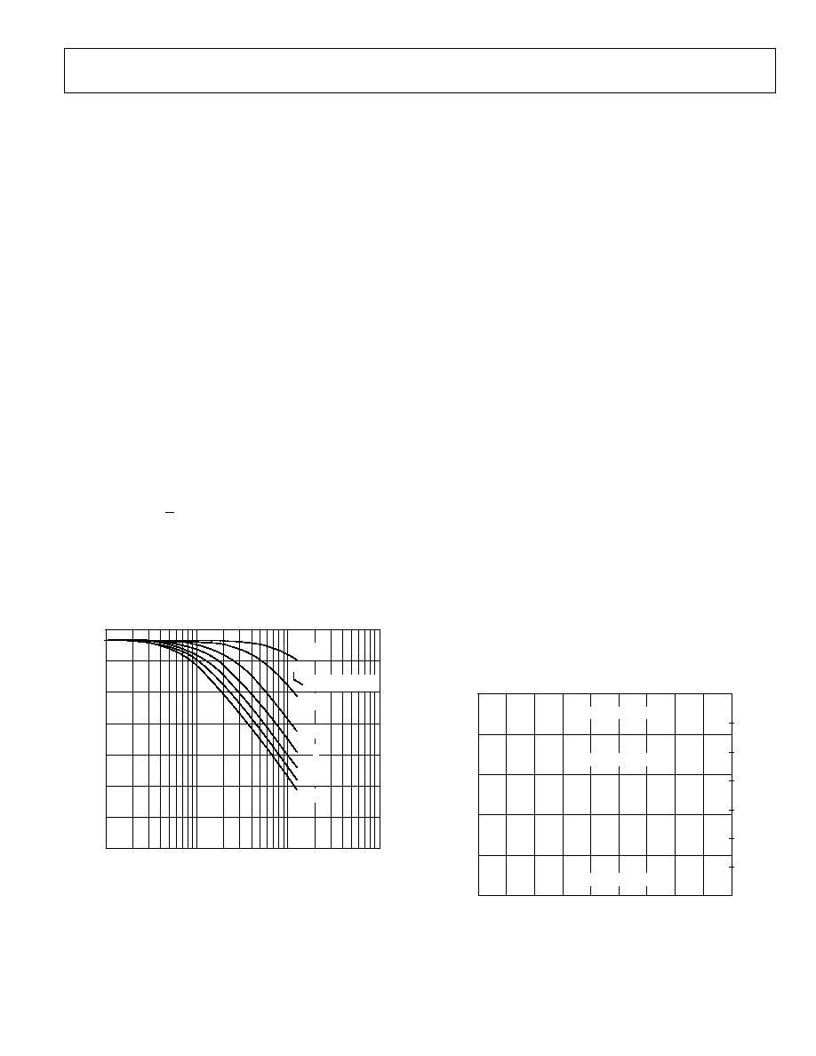
Jitter Considerations
High speed, high resolution ADCs are sensitive to the quality of
the clock input. The degradation in SNR at a given input fre-
quency (f
INPUT
) due only to aperture jitter (t
J
) can be calculated
by
×
=
J
INPUT
t
f
2
20
log
SNR
In the equation, the rms aperture jitter represents the root-mean
square of all jitter sources, which include the clock input, analog
input signal, and ADC aperture jitter specification. IF under-
sampling applications are particularly sensitive to jitter, see
Figure 6.
INPUT FREQUENCY (MHz)
1
40
75
70
65
60
55
50
45
1000
100
10
0.2ps
0.5ps
1.0ps
1.5ps
2.0ps
2.5ps
3.0ps
SNR (
d
Bc)
Figure 6. SNR vs. Input Frequency and Jitter
The clock input should be treated as an analog signal in cases
where aperture jitter may affect the dynamic range of the
AD9233. Power supplies for clock drivers should be separated
from the ADC output driver supplies to avoid modulating the
clock signal with digital noise. Low jitter, crystal-controlled
oscillators make the best clock sources. If the clock is generated
from another type of source (by gating, dividing, or other meth-
ods), it should be retimed by the original clock at the last step.
POWER DISSIPATION AND STANDBY MODE
As shown in Figure 7, the power dissipated by the AD9233 is
proportional to its sample rate. The digital power dissipation is
determined primarily by the strength of the digital drivers and
the load on each output bit. The maximum DRVDD current
(I
DRVDD
) can be calculated as
N
f
C
V
I
CLK
LOAD
DRVDD
DRVDD
×
×
×
=
where N is the number of output bits, 12 in the case of the
AD9233. This maximum current occurs when every output bit
switches on every clock cycle, that is, a full-scale square wave at
the Nyquist frequency, f
CLK
/2. In practice, the DRVDD current is
established by the average number of output bits switching,
which is determined by the sample rate and the characteristics
of the analog input signal. Reducing the capacitive load pre-
sented to the output drivers can minimize digital power con-
sumption. The data in Figure 7 was taken with the same operat-
ing conditions as the Typical Performance Characteristics and a
5 pF load on each output driver.
By asserting the PDWN pin high, the AD9233 is placed in
standby mode. In this state, the ADC typically dissipates
1 mW if the CLK and analog inputs are static. During standby,
the output drivers are placed in a high impedance state. Reas-
serting the PDWN pin low returns the AD9233 into its normal
operational mode.
SAMPLE RATE (MSPS)
10
20
30
40
50
60
70
80
90
300
325
350
375
400
425
0
20
40
60
80
100
120
140
100
ANALOG CURRENT
TOTAL POWER
DIGITAL CURRENT
Total P
o
wer (mW)
Curr
ent (mA)
Figure 7. Power and Current vs. Sample Rate @ 2.5 MHz
AD9233
Preliminary Technical Data
Rev. PrG | Page 12 of 19
Low power dissipation in standby mode is achieved by shutting
down the reference, reference buffer, and biasing networks. The
decoupling capacitors on REFT and REFB are discharged when
entering standby mode and then must be recharged when re-
turning to normal operation. As a result, the wake-up time is
related to the time spent in standby mode and shorter standby
cycles result in proportionally shorter wake-up times. With the
recommended 0.1 µF and 10 µF decoupling capacitors on REFT
and REFB, it takes approximately 1 sec to fully discharge the
reference buffer decoupling capacitors and 3 ms to restore full
operation.
DIGITAL OUTPUTS
The AD9233 output drivers can be configured to interface with
1.8 V to 3.3 V logic families by matching DRVDD to the digital
supply of the interfaced logic. The output drivers are sized to
provide sufficient output current to drive a wide variety of logic
families. However, large drive currents tend to cause current
glitches on the supplies that may affect converter performance.
Applications requiring the ADC to drive large capacitive loads
or large fan-outs may require external buffers or latches.
As detailed in Interfacing to ADC SPI, the data format can be
selected for either offset binary, twos complement, or Gray code
(SPI access only).
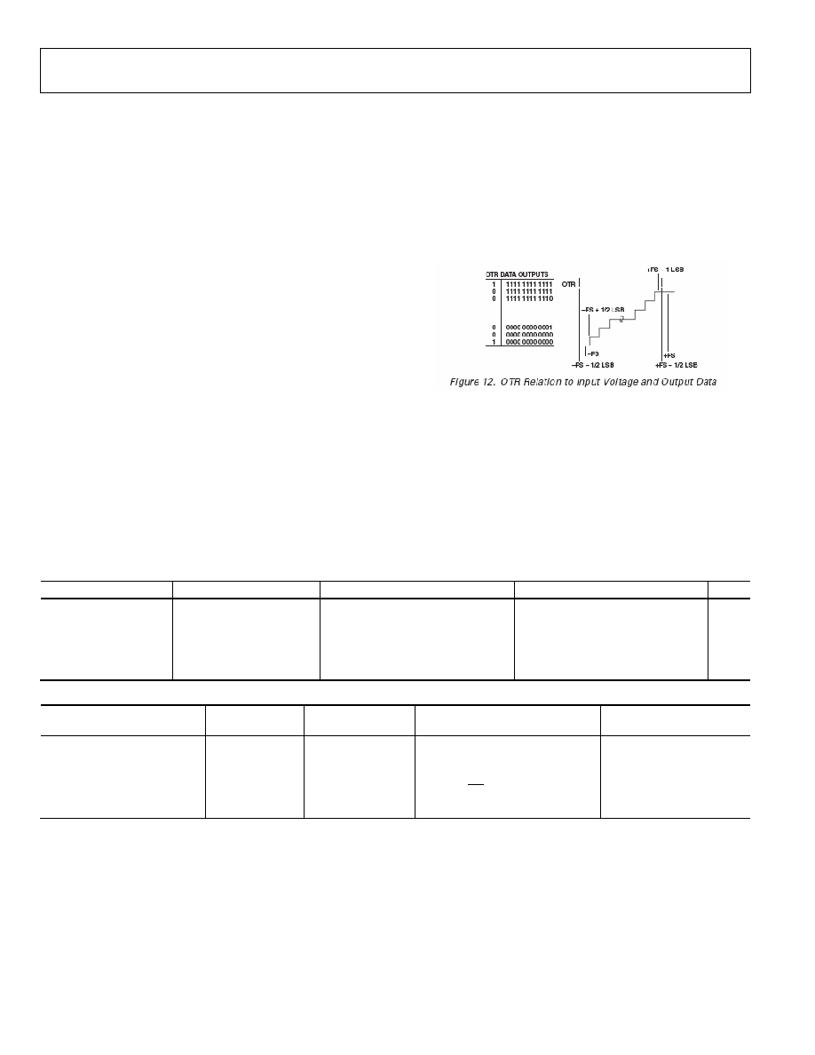
Out-of-Range (OTR)
An out-of-range condition exists when the analog input voltage
is beyond the input range of the ADC. OTR is a digital output
that is updated along with the data output corresponding to the
particular sampled input voltage. Thus, OTR has the same pipe-
line latency as the digital data. OTR is low when the analog in-
put voltage is within the analog input range and high when the
analog input voltage exceeds the input range as shown in Figure
8. OTR will remain high until the analog input returns to within
the input range and another conversion is completed. By logi-
cally AND-ing OTR with the MSB and its complement, over-
range high or underrange low conditions can be detected.
Figure 8. OTR Relation to Input Voltage and Output Data
TIMING
The AD9233 provides latched data outputs with a pipeline delay
of twelve clock cycles. Data outputs are available one propaga-
tion delay (t
PD
) after the rising edge of the clock signal.
Table 8. Table III. Output Data Format
Input (V)
Condition (V)
Binary Output Mode
Twos Complement Mode
OTR
VIN+ VIN
< VREF 0.5 LSB
0000 0000 0000
1000 0000 0000
1
VIN+ VIN
= VREF
0000 0000 0000
1000 0000 0000
0
VIN+ VIN
= 0
1000 0000 0000
0000 0000 0000
0
VIN+ VIN
= +VREF 1.0 LSB
1111 1111 1111
0111 1111 1111
0
VIN+ VIN
> +VREF 0.5 LSB
1111 1111 1111
0111 1111 1111
1
Table 9. Reference Configuration Summary
Selected Mode
SENSE
Voltage
Internal Switch
Position
Resulting VREF (V)
Resulting Differential
Span (V p-p)
External Reference
AVDD
N/A
N/A
2 × External Reference
Internal Fixed Reference
VREF
SENSE
0.5
1.0
Programmable Reference
0.2 V to VREF
SENSE
+
×
1
2
1
5
.
0
R
R
(See Figure 10)
2 × VREF
Internal Fixed Reference
AGND to 0.2 V
Internal Divider
1.0
2.0
Preliminary Technical Data
AD9233
Rev. PrG | Page 13 of 19
The length of the output data lines and loads placed on them
should be minimized to reduce transients within the AD9233.
These transients can degrade the converter's dynamic performance.
The AD9233 also provides data clock output (DCO) intended for
capturing the data in an external register. The data outputs are
valid on the rising edge of DCO.
The lowest typical conversion rate of the AD9233 is 10 MSPS.
At clock rates below 1 MSPS, dynamic performance can de-
grade.
Digital Output Enable Function (OEB)
The AD9233 has three-state ability. If the OEB pin is low, the
output data drivers are enabled. If the OEB pin is high, the out-
put data drivers are placed in a high impedance state. It is not
intended for rapid access to the data bus. Note that OEB is ref-
erenced to the digital supplies (DRVDD) and should not exceed
that supply voltage.
VOLTAGE REFERENCE
A stable and accurate 0.5 V voltage reference is built into the
AD9233. The input range can be adjusted by varying the refer-
ence voltage applied to the AD9233, using either the internal
reference or an externally applied reference voltage. The input
span of the ADC tracks reference voltage changes linearly. The
various reference modes are summarized in the next few sec-
tions.
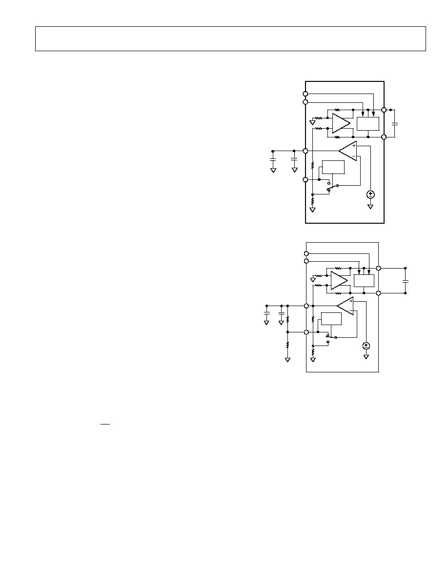
Internal Reference Connection
A comparator within the AD9233 detects the potential at the
SENSE pin and configures the reference into four possible
states, which are summarized in Table X. If SENSE is grounded,
the reference amplifier switch is connected to the internal resis-
tor divider (see Figure 9), setting VREF to 1 V. Connecting the
SENSE pin to VREF switches the reference amplifier output to
the SENSE pin, completing the loop and providing a 0.5 V ref-
erence output. If a resistor divider is connected as shown in
Figure 10, the switch again sets to the SENSE pin. This puts the
reference amplifier in a noninverting mode with the VREF out-
put defined as
+
×
=
1
2
1
5
0
R
R
.
VREF
The VREF pin should be externally decoupled to ground with a
low ESR 1.0uF capacitor in parallel with a 0.1uF cap. In all ref-
erence configurations, REFT and REFB drive the A/D converter
core and establish its input span. AN external 0.1uF capacitor
should be placed across REFT / REFB to stabilize this reference.
The input range of the ADC always equals twice the voltage at
the reference pin for either an internal or an external reference.
If the internal reference of the AD9233 is used to drive multiple
converters to improve gain matching, the loading of the refer-
ence by the other converters must be considered. Figure 11
depicts how the internal reference voltage is affected by loading.
0.1
uF
VREF
SENSE
0.5V
AD9233
VIN
VIN+
REFT
0.1
uF
REFB
SELECT
LOGIC
ADC
CORE
1.0
uF
Figure 9. Internal Reference Configuration
0.1
uF
VREF
SENSE
R2
R1
0.5V
AD923
VIN
VIN+
REFT
0.1
uF
REFB
SELECT
LOGIC
ADC
CORE
1.0
uF
Figure 10. Programmable Reference Configuration
External Reference Operation
The use of an external reference may be necessary to enhance
the gain accuracy of the ADC or improve thermal drift charac-
teristics. When multiple ADCs track one another, a single refer-
ence (internal or external) may be necessary to reduce gain
matching errors to an acceptable level. Figure 12 shows the typi-
cal drift characteristics of the internal reference in both 1 V and
0.5 V modes.
When the SENSE pin is tied to AVDD, the internal reference is
disabled, allowing the use of an external reference. An internal
reference buffer loads the external reference with an equivalent
TBD k load. The internal buffer still generates the positive and
negative full-scale references, REFT and REFB, for the ADC
core. The input span is always twice the value of the reference
voltage; therefore, the external reference must be limited to a
maximum of 1 V.
AD9233
Preliminary Technical Data
Rev. PrG | Page 14 of 19
LOAD (mA)
0.05
0
0.5
1.0
1.5
2.0
2.5
3.0
0
0.25
0.20
0.15
0.10
0.05
0.5V ERROR (%)
1V ERROR (%)
E
rro
r
(%
)
Figure 11. VREF Accuracy vs. Load
40
0
1.0
0.9
0.8
0.7
0.6
0.5
0.4
0.3
0.2
0.1
80
70
60
50
40
30
20
10
0
10
20
30
VREF = 0.5V
VREF = 1V
VREF
E
RRO
R(%)
Figure 12. Typical VREF Drift
RBIAS
The AD9233 requires the user to place a 10K resistor between
the RBIAS pin and ground. This resister should have a 1% tol-
erance, and is used to set the master current reference of the
ADC core.
AD9233 CONFIGURATION USING THE SPI
The AD9233 serial port interface allows the user to configure
the converter for specific functions or operations through a
structured register space inside the ADC. This gives the user
added flexibility to customize device opertation depending on
the application. Addresses are accessed (programmed or read
back) serially in one-byte words. Each byte may be further di-
vided down into fields which are documented in the Memory
Map Section below.
There are three pins that define the serial port interface or SPI
to this particular ADC. They are the SPI SCLK / DFS, SPI SDIO
/ DCS, and CSB pins. The SCLK/DFS (serial clock) is used to
synchronize the read and write data presented the ADC.. The
SDIO / DCS (serial data input/output) is a dual purpose pin
that allows data to be sent and read from the internal ADC
memory map registers. The CSB or chip select bar is an active
low control that enables or disables the read and write cycles.
See Table X.
Table X. Serial Port Pins
Pin Function
SCLK
SCLK (Serial Clock) is the serial shift clock in. SCLK is
used to synchronize serial interface reads and writes.
SDIO
SDIO (Serial Data Input/Output) is a dual purpose pin.
The typical role for this pin is an input and output de-
pending on the instruction being sent and the relative
position in the timing frame.
CSB
CSB (Chip Select Bar) is active low controls that gates
the read and write cycles.
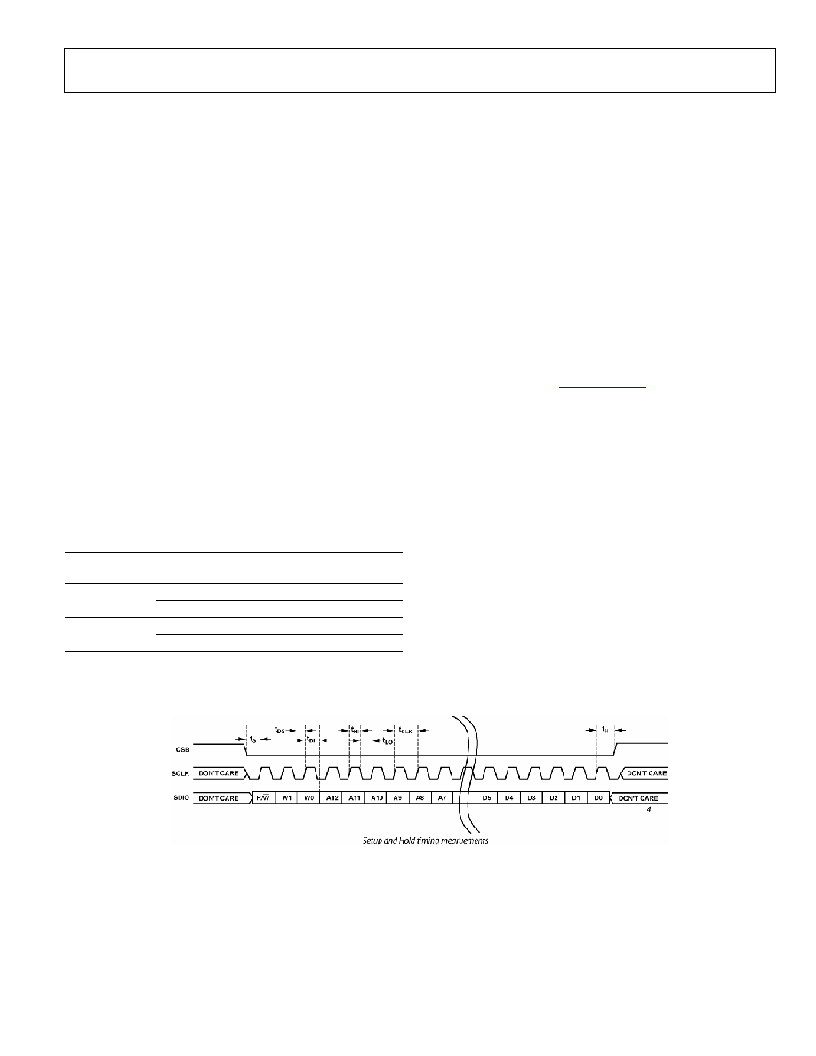
The falling edge of the CSB in conjunction with the rising edge
of the SCLK determines the start of the framing. An example of
the serial timing and its definitions can be found in Figure X
and Table X. Table X. SPI Timing Diagram specifications
Spec
Name
Meaning
t
DS
Setup time between data and rising edge of SCLK
t
DH
Hold time between data and rising edge of SCLK
t
CLK
Period of the clock
t
S
Setup time between CSB and SCLK
t
H
Hold time between CSB and SCLK
t
HI
Minimum period that SCLK should be in a logic high
state
t
LO
Minimum period that SCLK should be in a logic low
state
During an instruction phase a 16bit instruction is transmitted.
Data then follows the instruction phase and is determined by
the W0 and W1 bits which is 1 or more bytes of data. All data is
composed of 8bit words. The first bit of each individual byte of
serial data indicates whether this is a read or write command.
This allows the serial data input/output (SDIO) pin to change
direction from an input to an output.
Data may be sent in MSB or in LSB first mode. MSB first is de-
fault on power up and may be changed by changing the con-
figuration register. For more information about this feature and
others see SPI Doc at www.analog.com.
Preliminary Technical Data
AD9233
Rev. PrG | Page 15 of 19
HARDWARE INTERFACE
The pins described in Table X comprise the physical interface
between the user's programming device and the serial port of
the AD9233. All serial pins are inputs, which is an open-drain
output and should be tied to an external pull-up or pull-down
resistor (suggested value 10 k).
This interface is flexible enough to be controlled by either
PROMS or PIC mirocontrollers as well. This provides the user
to use an alternate method to program the ADC other than a
SPI controller.
If the user chooses to not use the SPI interface, some pins serve
a dual function and are associated with a specific function when
strapped externally to AVDD or ground during device power
on. The section below describes the strappable functions sup-
ported on the AD9233. AD9233
CONFIGURATION WITHOUT THE SPI
In applications that do not interface to the SPI control registers,
the SPI SDIO / DCS and SPI SCLK / DFS pins can alternately
serve as stand alone CMOS compatible control pins When the
device is powered up, it is assumed that the user intends to use
the pins as static control lines for the duty cycle stabilizer. In
this mode the SPI CSB chip select should be connected to
ground, which will disable the serial port interface.
Table 10. Mode Selection
Pin External
Voltage
Configuration
AVDD
Duty Cycle Stabilizer Enabled
SPI SDIO / DCS
AGND
Duty Cycle Stabilizer Disabled
AVDD
2's Complement Enabled
SPI SCLK / DFS
AGND
Offset Binary Enabled
READING THE MEMORY MAP TABLE
Each row in the memory map table has eight address locations.
The memory map is roughly divided into four sections: chip
configuration register map (Address 0x00 to Address 0x02),
device index and transfer register map (Address 0x04 to Ad-
dress 0x05, and Address 0xFF), global ADC function register
map (Address 0x08 to Address 0x09), and flexible ADC func-
tions register map (Address 0x0B to Address 0x25). The flexible
ADC functions register map is product specific.
Starting from the right hand column the memory map register
in Table X documents the default hex value for each hex ad-
dress shown. The column with the heading Byte 7 (MSB) is the
start of the default hex value giving. For example, hex address
0x14, flex_output_phase has a hex default value of 00h. This
means Bit 3 = 0, Bit 2 = 0, Bit 1 = 1, and Bit 0 = 1 or 0011 in
binary. This setting is the default output clock or DCO phase
adjust option. The default value adjusts the DCO phase 90deg
relative to the Nominal DCO edge and 180deg relative to the
data edge. For more information on this function and others
consult the SPI Doc at
www.analog.com
.
OPEN LOCATIONS
All locations marked as "open" are currently not supported for
this particular device. When required, these locations should be
written with 0s. Writing to these locations is required only when
part of an address location is open (for example, Address 0x14).
If the whole address location is open (for example, Address
0x13), then this address location does not need to be written.
DEFAULT VALUES
Coming out of reset, some of the address locations (but not all)
are loaded with default values. The default values for the regis-
ters are given in the Table X.
LOGIC LEVELS
An explanation of various registers, "bit is set" is synonymous
with "bit is set to Logic 1" or "writing Logic 1 for the bit." Simi-
larly "clear a bit" is synonymous with "bit is set to Logic 0" or
"writing Logic 0 for the bit."
Figure X. Serial Port Interface Timing Diagram
AD9233
Preliminary Technical Data
Rev. PrG | Page 16 of 19
Table X. AD9233 Device Configuration Register Memory Map
Addr
(Hex)
Parameter Name
Bit 7
(MSB)
Bit 6
Bit 5
Bit 4
Bit 3
Bit 2
Bit 1
Bit 0
(LSB)
Def.
Value
(Hex)
Default Notes
and comments
Chip Configuration Registers
00 chip_port_config OPEN LSB
First
Soft
Reset
OPEN OPEN
Soft
Reset
LSB
First
OPEN
18h The
nibbles
should be mir-
rored by the user
so that LSB or
MSB first mode
will register
correctly regard-
less of shift
mode.
01
chip_id
8-bit Chip ID bits 7:0
AD9233 01h
Read
only
Unique chip ID
02 chip_grade OPEN
Child ID
125MS -00h
105MS 08h
OPEN
Read
only
Read only. Child
ID used to dif-
ferentiate speed
grades.
Device Index and Transfer Registers
FF
device_update OPEN SW
Transfer
00h Synchronously
transfers data
from the master
shift register to
the slave
Global ADC Functions
08 global_modes
OPEN PWDN
Func-
tion
0 Full
Power
Down
1 -
Standb
y
OPEN
Internal Power Down Mode
0 normal (power up)
1 full power down
2 standby
3 normal (power up)
Note: External PWDN pin over-
rides internal power down mode
setting
00h Determines
various generic
modes of chip
operation.
09 global_clock
OPEN
Duty
Cycle
Stabi-
lizer
0-
disabled
1-
Enabled
01h
Flexible ADC Functions
Preliminary Technical Data
AD9233
Rev. PrG | Page 17 of 19
Addr
(Hex)
Parameter Name
Bit 7
(MSB)
Bit 6
Bit 5
Bit 4
Bit 3
Bit 2
Bit 1
Bit 0
(LSB)
Def.
Value
(Hex)
Default Notes
and comments
10
Digital Offset Adjust
10h<5:0> Offset in LSBs
011111 +7.75
011110 +7.50
011101 +7.25
.
.
.
000010 +0.5
000001 +0.25
000000 0
111111 -0.25
111110 -0.5
111101 -0.75
.
.
100001 -7.75
100000 -8.00
00h
0D flex_test_io
PN23
0=
normal
1=reset
PN9
0=
normal
1=reset
Global Output Test Options
0 off 1 midscale short
2 - +FS short 3 - -FS short
4 checker board output
5 PN 23 sequence 6 PN 9
7 one/zero word toggle
00h
When set, the
test data is placed
on the output
pins in place of
normal data
14 flex_output_mode
OPEN
Output
Disable
1- Ou-
puts
disabled
0 - Ou-
puts
Enabled
Note
External
OE/ pin
over
mist be
HIGH
OPEN
Output
Data
Invert
1=inver
t
Data Format
Select
0 offset binary
1 - 2's complement
3 Gray
4 offset binary
00h Configures
the
outputs and the
format of the
data.
16 flex_output_phase Output
Clock
Polarity
1=inver
ted
0=Nor
mal
OPEN 00h
17
flex_output_drive
RE-
SERVED
0
Output Driver Configuration
1000 for DrVDD =3.3V
1000 for DrVDD = V
1110 for DrVDD=1.8V
Reserved
000
70h
AD9233
Preliminary Technical Data
Rev. PrG | Page 18 of 19
Addr
(Hex)
Parameter Name
Bit 7
(MSB)
Bit 6
Bit 5
Bit 4
Bit 3
Bit 2
Bit 1
Bit 0
(LSB)
Def.
Value
(Hex)
Default Notes
and comments
18 flex_vref
Internal Reference
Resistor Divider
00 VREF=1.25V
01 VREF=1.5V
10 VREF=1.75V
11 VREF=2.00V
Open 0Ch
Power and Ground Recommendations
When connecting power to the AD9246, it is recommended that
two separate supplies be used: one for analog (AVDD, 1.8V
nominal) and one for digital (DRVDD, 1.8-3.3V nominal). If
only a single 1.8V supply is available, then it should be routed to
the AVDD first and tapped off and isolated with a ferrite bead
or filter choke with decoupling capacitors proceeding its con-
nection to DrVDD. The user can employ several different de-
coupling capacitors to cover both high and low frequencies.
These should be located close to the point of entry at the PC
board level and close to the parts with minimal trace length.
A single PC board ground plane should be sufficient when us-
ing the AD9246. With proper decoupling and smart parti-
tioning of the PC board's analog, digital, and clock sections,
optimum performance is easily achieved.
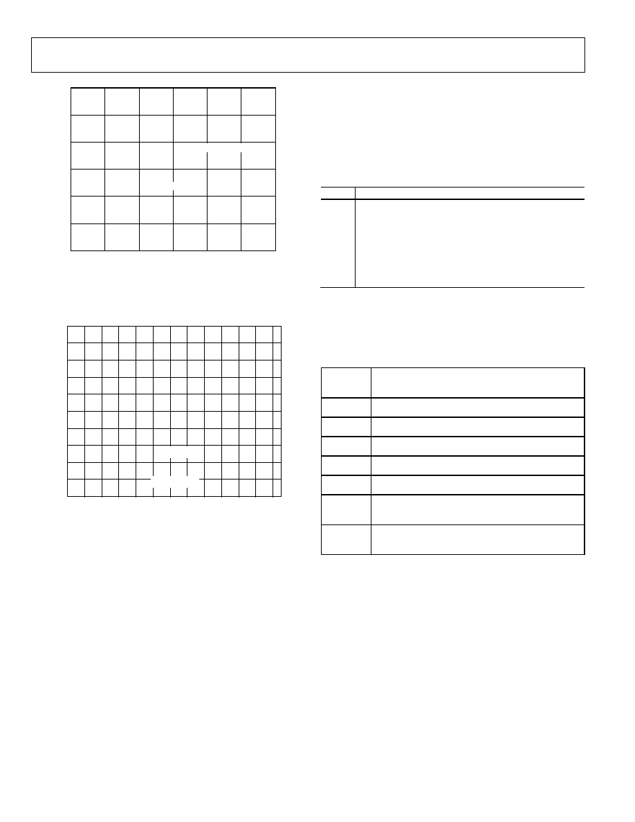
Exposed Paddle Thermal Heat Slug Recommendations
It is mandatory that the exposed paddle on the underside of the
ADC is connected to analog ground (AGND) to achieve the
best electrical and thermal performance of the AD9228. A con-
tinuous exposed (no solder mask) copper plane on the PCB
should mate to the AD9246 exposed paddle, Pin 0. The copper
plane should have several vias to achieve the lowest possible
resistive thermal path for heat dissipation to flow through the
bottom of the PCB. These vias should be solder filled or
plugged.
To maximize the coverage and adhesion between the ADC and
PCB, overlay a silkscreen to partition the continuous plane on
the PCB into several uniform sections. This provides several tie
points between the two during the reflow process. Using one
continuous plane with no partitions only guarantees one tie
point between the ADC and PCB. See Figure for a PCB layout
example. For detailed information on packaging and the PCB
layout of chip scale packages, go to
www.analog.com
.
SILKSCREEN PARTITION
PIN 1 INDICATOR
04418-
052
Figure 6. Typical PCB Layout
Preliminary Technical Data
AD9233
Rev. PrG | Page 19 of 19
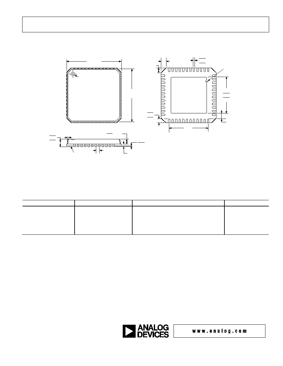
OUTLINE DIMENSIONS
PIN 1
INDICATOR
TOP
VIEW
6.75
BSC SQ
7.00
BSC SQ
1
48
12
13
37
36
24
25
5.25
5.10 SQ
4.95
0.50
0.40
0.30
0.30
0.23
0.18
0.50 BSC
12° MAX
0.20 REF
0.80 MAX
0.65 TYP
1.00
0.85
0.80
5.50
REF
0.05 MAX
0.02 NOM
0.60 MAX
0.60 MAX
PIN 1
INDICATOR
COPLANARITY
0.08
SEATING
PLANE
0.25 MIN
EXPOSED
PAD
(BOTTOM VIEW)
COMPLIANT TO JEDEC STANDARDS MO-220-VKKD-2
Figure 13. 48-Lead Frame Chip Scale Package [LFCSP_VQ]
7 mm × 7 mm Body, Very Thin Quad (CP-48-1)
Dimensions shown in millimeters
ORDERING GUIDE
Model
Temperature Package
Package Description
Package Outline
AD9233BCPZ-125
1
40°C to +85°C
48-Lead Lead Frame Chip Scale Package
CP-48-1
AD9233BCPZRL7125
1
40°C to +85°C
48-Lead Lead Frame Chip Scale Package
CP-48-1
AD9233BCPZ-105
1
40°C to +85°C
48-Lead Lead Frame Chip Scale Package
CP-48-1
AD9233BCPZRL7105
1
40°C to +85°C
48-Lead Lead Frame Chip Scale Package
CP-48-1
AD9233BCPZ-125EB
1
Evaluation
Board
1
It is recommended that the exposed paddle be soldered to the ground plane for the LFCSP package. There is an increased reliability of the solder joints, and the maxi-
mum thermal capability of the package is achieved with the exposed paddle soldered to the customer board.
©2005 Analog Devices, Inc. All rights reserved. Trademarks and
registered trademarks are the property of their respective owners.
(PrG)