 | –≠–ª–µ–∫—Ç—Ä–æ–Ω–Ω—ã–π –∫–æ–º–ø–æ–Ω–µ–Ω—Ç: AD9238 | –°–∫–∞—á–∞—Ç—å:  PDF PDF  ZIP ZIP |
ƒÓÍÛÏÂÌÚýˆËˇ Ë ÓÔËÒýÌˡ www.docs.chipfind.ru
Information furnished by Analog Devices is be lieved to be accurate and
reliable. However, no responsibility is assumed by Analog Devices for its
use, nor for any infringements of patents or other rights of third parties
that may result from its use. No license is granted by implication or oth-
erwise under any patent or patent rights of Analog Devices. Trademarks
and registered trademarks are the property of their respective owners.
One Technology Way, P.O. Box 9106, Norwood, MA 02062-9106, U.S.A.
Tel: 781/329-4700
www.analog.com
Fax: 781/326-8703 © 2003 Analog Devices, Inc. All rights reserved.
AD9238
12-Bit, 20/40/65 MSPS
Dual A/D Converter
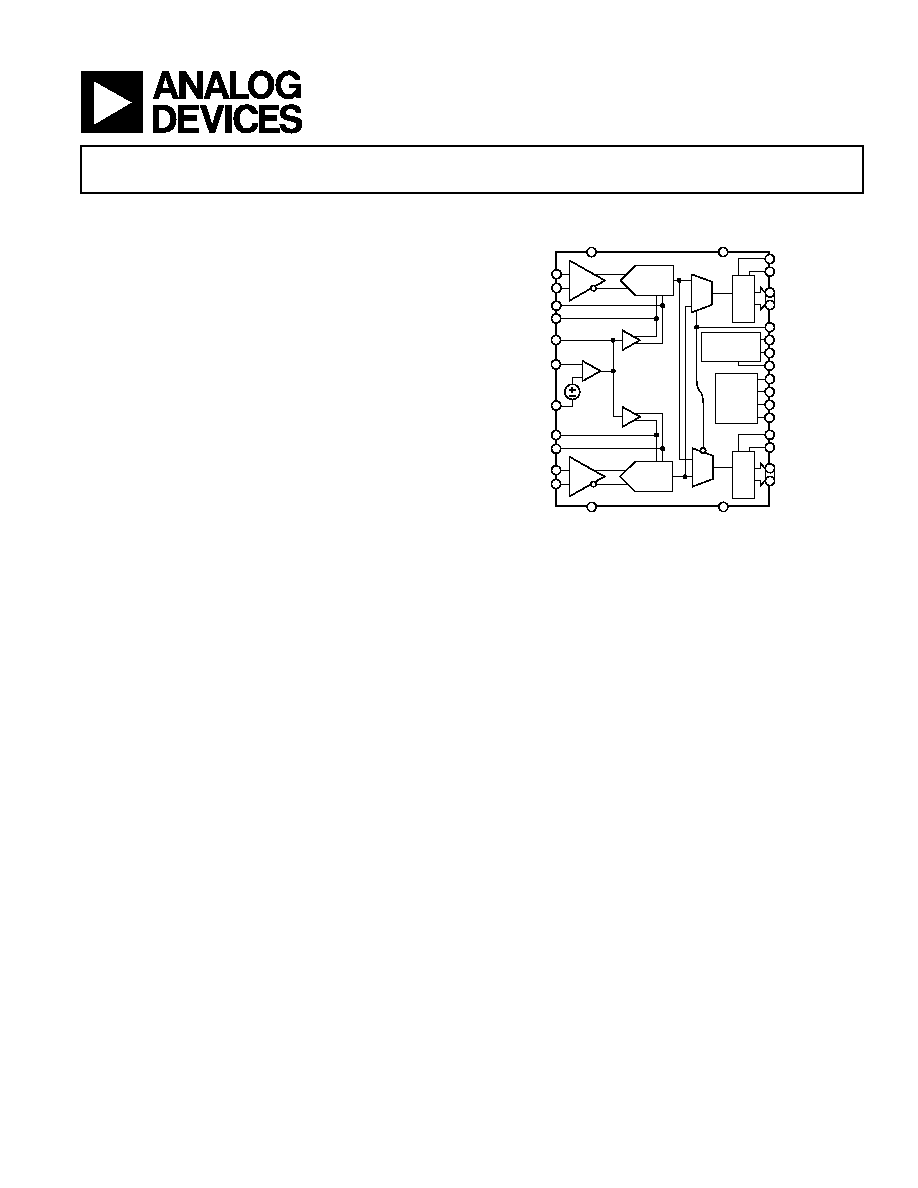
FUNCTIONAL BLOCK DIAGRAM
SHA
A/D
SHA
A/D
CLOCK
DUTY CYCLE
STABILIZER
MODE
SELECT
OEB_A
OTR_A
D11_A
D0_A
MUX_SELECT
CLK_A
CLK_B
DCS
DFS
PDWN_A
PDWN_B
SHARED_REF
OEB_B
OTR_B
D11_B
D0_B
DRGND
AGND
DRVDD
AVDD
0.5V
VIN+_A
VIN≠_A
REFT_A
REFB_A
VREF
SENSE
AGND
REFB_B
REFT_B
VIN≠_B
VIN+_B
O/P
BUFFERS
O/P
BUFFERS
FEATURES
Integrated Dual 12-Bit Analog-to-Digital Converters
Single 3 V Supply Operation (2.7 V to 3.6 V)
SNR = 70 dBc (to Nyquist, AD9238-65)
SFDR = 85 dBc (to Nyquist, AD9238-65)
Low Power: 600 mW at 65 MSPS
Differential Input with 500 MHz 3 dB Bandwidth
On-Chip Reference and SHA
Flexible Analog Input: 1 V p-p to 2 V p-p Range
Offset Binary or Twos Complement Data Format
Clock Duty Cycle Stabilizer
APPLICATIONS
Ultrasound Equipment
IF Sampling in Communications Receivers:
IS-95, CDMA One, IMT-2000
Battery-Powered Instruments
Hand-Held Scopemeters
Low Cost Digital Oscilloscopes
PRODUCT HIGHLIGHTS
1. Integrated, dual version of the AD9235--a 12-bit,
20 MSPS/40 MSPS/65 MSPS ADC.
2. Speed grade options of 20 MSPS, 40 MSPS, and 65 MSPS
allow fl exibility between power, cost, and performance to suit
an application.
3. The AD9238 operates from a single 3 V power supply and
features a separate digital output driver supply to accommo-
date 2.5 V and 3.3 V logic families.
4. Low power consumption:
AD9238-20 operating at 20 MSPS consumes a low 180 mW.
AD9238-40 operating at 40 MSPS consumes a low 330 mW.
AD9238-65 operating at 65 MSPS consumes a low 600 mW.
5. The patented SHA input maintains excellent performance for
input frequencies up to 100 MHz and can be confi gured for
single-ended or differential operation.
6. Typical channel isolation of 80 dB @ f
IN
= 10 MHz.
7. The clock duty cycle stabilizer (AD9238-65 only) maintains
performance over a wide range of clock duty cycles.
8. The OTR output bits indicate when either input signal is
beyond the selected input range.
9. Multiplexed data output option enables single-port operation
from either data port A or data port B.
GENERAL DESCRIPTION
The AD9238 is a dual, 3 V, 12-bit, 20 MSPS/40 MSPS/65 MSPS
analog-to-digital converter. It features dual high performance
sample-and-hold amplifi ers and an integrated voltage reference.
The AD9238 uses a multistage differential pipelined architecture
with output error correction logic to provide 12-bit accuracy and
guarantee no missing codes over the full operating temperature
range at data rates up to 65 MSPS.
The wide bandwidth, differential SHA allows for a variety of
user selectable input ranges and offsets including single-ended
applications. It is suitable for various applications including multi-
plexed systems that switch full-scale voltage levels in successive
channels and for sampling inputs at frequencies well beyond the
Nyquist rate. The AD9238 is suitable for applications in commu-
nications, imaging, and medical ultrasound.
Dual single-ended clock inputs are used to control all internal con-
version cycles. A duty cycle stabilizer is available on the AD9238-65
and can compensate for wide variations in the clock duty cycle,
allowing the converters to maintain excellent performance. The
digital output data is presented in either straight binary or twos
complement format. Out-of-range signals indicate an overfl ow
condition, which can be used with the most signifi cant bit to deter-
mine low or high overfl ow.
Fabricated on an advanced CMOS process, the AD9238 is avail-
able in a space saving 64-lead LQFP and is specifi ed over the
industrial temperature range (≠40∞C to +85∞C).
REV. A

≠2≠
AD9238≠SPECIFICATIONS
(AVDD = 3 V, DRVDD = 2.5 V, Maximum Sample Rate, CLK_A = CLK_B; AIN = ≠0.5 dBFS Differential Input,
1.0 V Internal Reference, T
MIN
to T
MAX
, un less oth er wise noted.)
DC SPECIFICATIONS
Test AD9238BST-20 AD9238BST-40 AD9238BST-65
Parameter
Temp Level Min Typ Max Min Typ
Max Min Typ
Max
Unit
RESOLUTION
Full VI 12
12
12
Bits
ACCURACY
No Missing Codes Guaranteed
Full VI 12
12
12
Bits
Offset Error
Full VI
±0.30 ±1.2
±0.50 ±1.1
±0.50 ±1.1
% FSR
Gain Error
1
Full IV
±0.30 ±2.2
±0.50 ±2.4
±0.50 ±2.5
% FSR
Differential Nonlinearity (DNL)
2
Full V
±0.35
±0.35
±0.35
LSB
25 C I
±0.35 ±0.9
±0.35 ±0.8
±0.35 ±1.0
LSB
Integral Nonlinearity (INL)
2
Full V
±0.45
±0.60
±0.70
LSB
25 C I
±0.40 ±1.4
±0.50 ±1.4
±0.55 ±1.75 LSB
TEMPERATURE DRIFT
Offset Error
Full V
±2
±2
±3
ppm/∞C
Gain Error
1
Full V
±12
±12
±12
ppm/∞C
INTERNAL VOLTAGE REFERENCE
Output Voltage Error (1 V Mode)
Full VI
±5 ±35
±5
±35
±5
±35
mV
Load Regulation @ 1.0 mA
Full V
0.8
0.8
0.8
mV
Output Voltage Error (0.5 V Mode)
Full V
±2.5
±2.5
±2.5
mV
Load Regulation @ 0.5 mA
Full V
0.1
0.1
0.1
mV
INPUT REFERRED NOISE
Input Span = 1 V
25 C V
0.54
0.54
0.54
LSB rms
Input Span = 2.0 V
25 C V
0.27
0.27
0.27
LSB rms
ANALOG INPUT
Input Span = 1.0 V
Full IV
1
1
1
V p-p
Input Span = 2.0 V
Full IV
2
2
2
V p-p
Input Capacitance
3
Full V
7
7
7
pF
REFERENCE INPUT RESISTANCE Full V
7
7
7
k
POWER SUPPLIES
Supply Voltages
AVDD
Full IV 2.7
3.0 3.6 2.7
3.0
3.6 2.7
3.0
3.6
V
DRVDD
Full IV 2.25 3.0 3.6 2.25 3.0
3.6 2.25 3.0
3.6
V
Supply Current
IAVDD
2
Full V
60
110
200
mA
IDRVDD
2
Full V
4
10
14
mA
PSRR
Full V
±0.01
±0.01
±0.01
% FSR
POWER CONSUMPTION
DC Input
4
Full V
180
330
600
mW
Sine Wave Input
2
Full VI
190 212
360
397
640
698
mW
Standby Power
5
Full V
2.0
2.0
2.0
mW
MATCHING CHARACTERISTICS
Offset Error
Full V
±0.1
±0.1
±0.1
% FSR
Gain Error
Full V
±0.05
±0.05
±0.05
% FSR
NOTES
1
Gain error and gain temperature coeffi cient are based on the A/D converter only (with a fi xed 1.0 V external reference).
2
Measured at maximum clock rate with a low frequency sine wave input and approximately 5 pF loading on each output bit.
3
Input capacitance refers to the effective capacitance between one differential input pin and AVSS. Refer to Figure 2 for the equivalent analog input structure.
4
Measured with dc input at maximum clock rate.
5
Standby power is measured with the CLK_A and CLK_B pins inactive (i.e., set to AVDD or AGND).
Specifi cations subject to change without notice.
REV. A

AD9238
≠3≠
DC SPECIFICATIONS
Test AD9238BST-20
AD9238BST-40 AD9238BST-65
Parameter Temp Level Min
Typ Max
Min
Typ Max Min
Typ
Max Unit
LOGIC INPUTS
High Level Input Voltage Full
IV 2.0
2.0
2.0
V
Low Level Input Voltage Full
IV
0.8
0.8
0.8
V
High Level Input Current Full
IV ≠10
+10
≠10
+10 ≠10
+10
µA
Low Level Input Current Full
IV ≠10
+10
≠10
+10 ≠10
+10
µA
Input Capacitance Full
V
2
2
2
pF
LOGIC OUTPUTS*
DRVDD = 3.3 V
High Level Output Voltage Full
IV 3.29
3.29
3.29
V
(IOH = 50 mA)
High Level Output Voltage Full
IV 3.25
3.25
3.25
V
(IOH = 0.5 mA)
Low Level Output Voltage Full
IV
0.05
0.05
0.05
V
(IOL = 50 mA)
Low Level Output Voltage Full
IV
0.2
0.2
0.2
V
(IOL = 1.6 mA)
DRVDD = 2.5 V
High Level Output Voltage Full
IV 2.49
2.49
2.49
V
(IOH = 50 mA)
High Level Output Voltage Full
IV 2.45
2.45
2.45
V
(IOH = 0.5 mA)
Low Level Output Voltage Full
IV
0.05
0.05
0.05
V
(IOL = 50 mA)
Low Level Output Voltage Full
IV
0.2
0.2
0.2
V
(IOL = 1.6 mA)
*Output Voltage Levels measured with 5 pF load on each output.
Specifi cations subject to change without notice.
SWITCHING SPECIFICATIONS
Test AD9238BST-20
AD9238BST-40 AD9238BST-65
Parameter Temp Level Min
Typ Max
Min
Typ Max Min
Typ
Max Unit
SWITCHING PERFORMANCE
Max Conversion Rate Full
VI 20
40
65
MSPS
Min Conversion Rate Full
V
1
1
1
MSPS
CLK Period Full
V 50.0
25.0
15.4
ns
CLK Pulsewidth High
1
Full
V 15.0
8.8
6.2
ns
CLK Pulsewidth Low
1
Full
V 15.0
8.8
6.2
ns
DATA OUTPUT PARAMETERS
Output Delay
2
(t
PD
) Full
IV 2
3.5 6
2
3.5 6 2
3.5
6
ns
Pipeline Delay (Latency) Full
V
7
7
7
Cycles
Aperture Delay (t
A
) Full V
1.0
1.0
1.0
ns
Aperture Uncertainty (t
J
) Full
V
0.5
0.5
0.5
ps rms
Wake-Up Time
3
Full
V
2.5
2.5
2.5
ms
OUT-OF-RANGE RECOVERY TIME Full
V
1
1
2
Cycles
NOTES
1
The AD9238-65 model has a duty cycle stabilizer circuit that, when enabled, corrects for a wide range of duty cycles (see TPC 20).
2
Output delay is measured from CLOCK 50% transition to DATA 50% transition, with a 5 pF load on each output.
3
Wake-up time is dependent on the value of the decoupling capacitors; typical values shown with 0.1 µF and 10 µF capacitors on REFT and REFB.
Specifi cations subject to change without notice.
(continued)
REV. A
≠4≠
AD9238
AC SPECIFICATIONS
Test AD9238BST-20 AD9238BST-40 AD9238BST-65
Parameter
Temp Level Min
Typ Max Min
Typ Max Min Typ
Max
Unit
SIGNAL-TO-NOISE RATIO
f
INPUT
f
f
= 2.4 MHz
25∞C V
70.4
70.4 70.3
dBc
f
INPUT
f
f
= 9.7 MHz
Full V
70.2
dBc
25∞C IV 69.7
70.4
dBc
f
INPUT
f
f
= 19.6 MHz
Full V
70.1
dBc
25∞C IV
69.7
70.3
dBc
f
INPUT
f
f
= 32.5 MHz
Full V
69.3
dBc
25∞C IV
68.7 69.5
dBc
f
INPUT
f
f
= 100 MHz
25∞C V
68.7
68.3 67.6
dBc
SIGNAL-TO-NOISE AND
DISTORTION RATIO
f
INPUT
f
f
= 2.4 MHz
25∞C V
70.2
70.2 70.1
dBc
f
INPUT
f
f
= 9.7 MHz
Full V
70.1
dBc
25∞C IV 69.3
70.2
dBc
f
INPUT
f
f
= 19.6 MHz
Full V
69.9
dBc
25∞C IV
69.4
70.1
dBc
f
INPUT
f
f
= 32.5 MHz
Full V
68.9
dBc
25∞C IV
68.1 69.1
dBc
f
INPUT
f
f
= 100 MHz
25∞C V
67.9
67.9 66.6
dBc
TOTAL HARMONIC
DISTORTION
f
INPUT
f
f
= 2.4 MHz
25∞C V
≠83.0
≠83.0 ≠83.0
dBc
f
INPUT
f
f
= 9.7 MHz
Full V
≠81.0
dBc
25∞C I
≠83.0 ≠74.6
dBc
f
INPUT
f
f
= 19.6 MHz
Full V
≠81.0
dBc
25∞C I
≠83.0 ≠75.5
dBc
f
INPUT
f
f
= 32.5 MHz
Full V
≠78.0
dBc
25∞C I
≠80.0
≠71.7 dBc
f
INPUT
f
f
= 100 MHz
25∞C V
≠77.0
≠79.0 ≠74.0
dBc
WORST HARMONIC
(2nd or 3rd)
f
INPUT
f
f
= 9.7 MHz
Full V
≠84.0
dBc
f
INPUT
f
f
= 19.6 MHz
Full V
≠85.0
dBc
f
INPUT
f
f
= 32.5 MHz
Full V
≠80.0
dBc
SPURIOUS FREE
DYNAMIC RANGE
f
INPUT
f
f
= 2.4 MHz
25∞C V
86.0
86.0 86.0
dBc
f
INPUT
f
f
= 9.7 MHz
Full V
84.0
dBc
25∞C I 76.1
86.0
dBc
f
INPUT
f
f
= 19.6 MHz
Full V
85.0
dBc
25∞C I
76.7
86.0
dBc
f
INPUT
f
f
= 32.5 MHz
Full V
80.0
dBc
25∞C I
72.5 83.0
dBc
f
INPUT
f
f
= 100 MHz
25∞C V
79.0
81.0 75.0
dBc
CROSSTALK
Full V
≠80
≠80 ≠80
dB
Specifi cations subject to change without notice.
(AVDD = 3 V, DRVDD = 2.5 V, Maximum Sample Rate, CLK_A = CLK_B; AIN = ≠0.5 dBFS Differential Input,
1.0 V Internal Reference, T
MIN
to T
MAX
, un less oth er wise noted.)
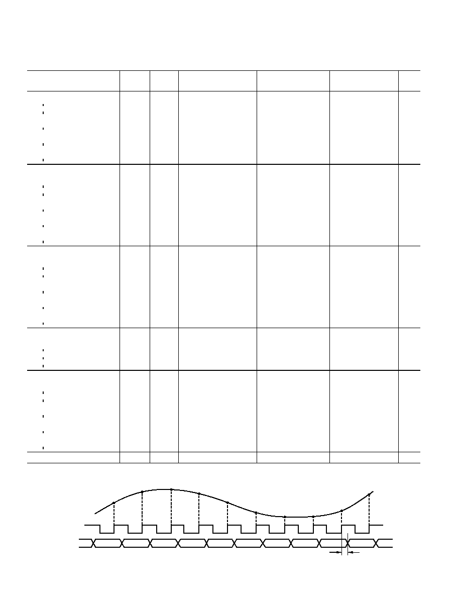
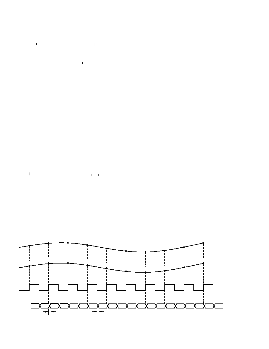
Figure 1. Timing Diagram
REV. A

AD9238
≠5≠
CAUTION
ESD (electrostatic discharge) sensitive device. Electrostatic charges as high as 4000 V readily ac cu mu late on
the human body and test equipment and can discharge without detection. Although the AD9238 features
proprietary ESD pro tec tion circuitry, permanent damage may occur on devices subjected to high energy
electrostatic discharges. Therefore, proper ESD pre cau tions are rec om mend ed to avoid per for mance
deg ra da tion or loss of functionality.
EXPLANATION OF TEST LEVELS
I 100% production tested.
II 100% production tested at 25∞C and sample tested at specifi ed
temperatures.
III Sample tested only.
IV Parameter is guaranteed by design and characterization testing.
V Parameter is a typical value only.
VI 100% production tested at 25∞C; guaranteed by design and
characterization testing for industrial temperature range; 100%
production tested at temperature extremes for military devices.
ABSOLUTE MAXIMUM RATINGS
1
With
Respect
Pin Name To
Min Max Unit
ELECTRICAL
AVDD AGND
≠0.3 +3.9 V
DRVDD DRGND ≠0.3 +3.9 V
AGND DRGND ≠0.3 +0.3 V
AVDD DRVDD
≠3.9 +3.9 V
Digital Outputs DRGND ≠0.3 DRVDD + 0.3 V
CLK, DCS,
MUX_SELECT,
SHARED_REF,
OEB, DFS AGND
≠0.3 AVDD + 0.3 V
VINA, VINB AGND
≠0.3 AVDD + 0.3 V
VREF AGND
≠0.3 AVDD + 0.3 V
SENSE AGND
≠0.3 AVDD + 0.3 V
REFB, REFT AGND
≠0.3 AVDD + 0.3 V
PDWN AGND
≠0.3 AVDD + 0.3 V
ENVIRONMENTAL
2
Operating Temperature
≠45 +85 ∞C
Junction Temperature
+150 ∞C
Lead Temperature (10 sec)
+300 ∞C
Storage Temperature
≠65 +150 ∞C
NOTES
1
Absolute maximum ratings are limiting values to be applied individually, and beyond
which the serviceability of the circuit may be impaired. Functional operability is
not necessarily implied. Exposure to absolute maximum rating conditions for an
extended period of time may affect device reliability.
2
Typical thermal impedances (64-lead LQFP);
JA
= 54∞C/W. These measurements
were taken on a 4-layer board in still air, in accordance with EIA/JESD51-7.
ORDERING GUIDE
Model Temperature Range Package Description Package Option
AD9238BST-20 ≠40∞C to +85∞C 64-Lead Low Profi le Quad Flat Pack (LQFP) ST-64-1
AD9238BST-40 ≠40∞C to +85∞C 64-Lead Low Profi le Quad Flat Pack (LQFP) ST-64-1
AD9238BST-65 ≠40∞C to +85∞C 64-Lead Low Profi le Quad Flat Pack (LQFP) ST-64-1
AD9238BSTRL-20 ≠40∞C to +85∞C 64-Lead Low Profi le Quad Flat Pack (LQFP) ST-64-1
AD9238BSTRL-40 ≠40∞C to +85∞C 64-Lead Low Profi le Quad Flat Pack (LQFP) ST-64-1
AD9238BSTRL-65 ≠40∞C to +85∞C 64-Lead Low Profi le Quad Flat Pack (LQFP) ST-64-1
AD9238-20PCB Evaluation Board with AD9238BST-20
AD9238-40PCB Evaluation Board with AD9238BST-40
AD9238-65PCB Evaluation Board with AD9238BST-65
REV. A
AD9238
≠6≠
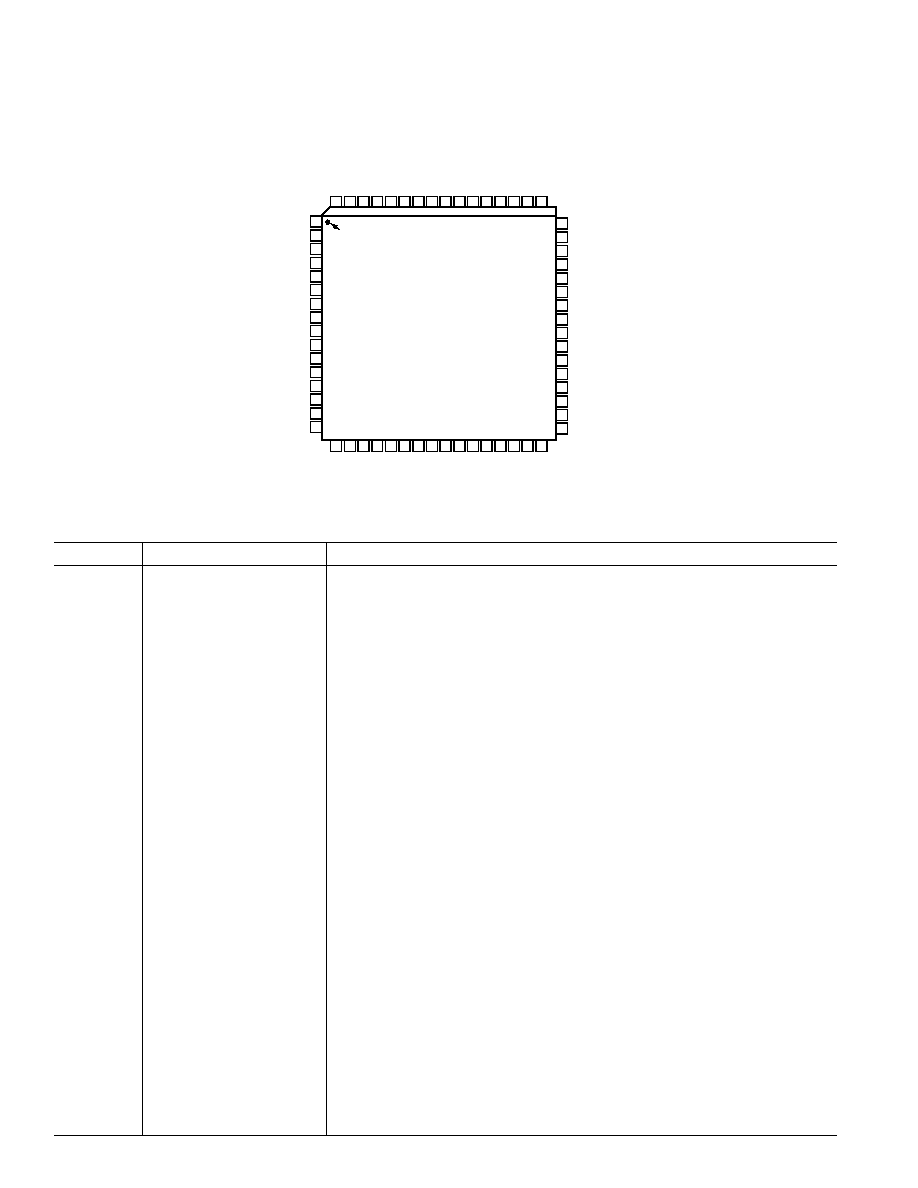
PIN FUNCTION DESCRIPTIONS
Pin Number Mnemonic Description
2 VIN+_A Analog Input Pin (+) for Channel A
3 VIN≠_A Analog Input Pin (≠) for Channel A
15 VIN+_B Analog Input Pin (+) for Channel B
14 VIN≠_B Analog Input Pin (≠) for Channel B
6 REFT_A Differential Reference (+) for Channel A
7 REFB_A Differential Reference (≠) for Channel A
11 REFT_B Differential Reference (+) for Channel B
10 REFB_B Differential Reference (≠) for Channel B
8 VREF Voltage Reference Input/Output
9 SENSE Reference Mode Selection
18 CLK_B Clock Input Pin for Channel B
63 CLK_A Clock Input Pin for Channel A
19 DCS Enable Duty Cycle Stabilizer (DCS) Mode
20 DFS Data Output Format Select Bit (Low for Offset Binary, High for Twos Complement)
21 PDWN_B Power-Down Function Selection for Channel B (Active High)
60 PDWN_A Power-Down Function Selection for Channel A (Active High)
22 OEB_B Output Enable Bit for Channel B
59 OEB_A Output Enable Bit for Channel A (Low Setting Enables Channel A Output Data Bus)
44≠51, 54≠57 D0_A (LSB)≠D11_A (MSB) Channel A Data Output Bits
25≠27, 30≠38 D0_B (LSB)≠D11_B (MSB) Channel B Data Output Bits
39 OTR_B Out-of-Range Indicator for Channel B
58 OTR_A Out-of-Range Indicator for Channel A
62 SHARED_REF Shared Reference Control Bit (Low for Independent Reference Mode,
High for Shared Reference Mode)
61 MUX_SELECT Data Multiplexed Mode. (See description for how to enable; high setting disables
output data Multiplexed mode).
5, 12, 17, 64 AVDD Analog Power Supply
1, 4, 13, 16 AGND Analog Ground
28, 40, 53 DRGND Digital Output Ground
29, 41, 52 DRVDD Digital Output Driver Supply. Must be decoupled to DRGND with a minimum
0.1 µF capacitor. Recommended decoupling is 0.1 µF capacitor in parallel with 10 µF.
23, 24, 42, 43 DNC Do Not Connect Pins. Should be left fl oating.
PIN CONFIGURATION
1
2
3
4
5
6
7
8
9
10
11
13
14
15
16
12
17 18 19 20 21 22 23 24 25 26 27 28 29 30 31 32
48
47
46
45
44
43
42
41
40
39
38
37
36
35
34
33
64 63 62 61 60
55 54 53 52 51 50 49
59 58 57 56
PIN 1
IDENTIFIER
64-LEAD LQFP
TOP VIEW
(Not to Scale)
D4_A
D3_A
D2_A
D1_A
D0_A
DNC
DNC
DRGND
OTR_B
D11_B (MSB)
D10_B
D9_B
D8_B
D7_B
D6_B
AD9238
AGND
AVDD
REFT_A
REFB_A
VREF
SENSE
REFB_B
AGND
VIN≠_B
VIN+_B
VIN+_A
VIN≠_A
AVDD
REFT_B
CLK_A
SHARED_REF
MUX_SELECT
OEB_A
D11_A (MSB)
D10_A
D9_A
D8_A
DRGND
D7_A
D6_A
D5_A
CLK_B
DC
S
DFS
PDWN_B
OEB_B
DN
C
D0_B
D1_B
D2_B
DRGND
D3_B
D4_B
D5_B
DN
C
AGND
AGND
AVDD
DRVDD
DRVDD
AVDD
PDWN_A
OTR_A
DRVDD
DNC = DO NOT CONNECT
REV. A

AD9238
≠6≠
AD9238
≠7≠
TERMINOLOGY
Aperture Delay
Aperture delay is a measure of the sample-and-hold amplifier
(SHA) performance and is measured from the rising edge of the
clock input to when the input signal is held for conversion.
Aperture Jitter
The variation in aperture delay for successive samples, which is
manifested as noise on the input to the A/D converter.
Integral Nonlinearity (INL)
INL refers to the deviation of each individual code from a line
drawn from negative full scale through positive full scale. The
point used as negative full scale occurs 1/2 LSB before the first
code transition. Positive full scale is defined as a level 1 1/2 LSB
beyond the last code transition. The deviation is measured from
the middle of each particular code to the true straight line.
Differential Nonlinearity (DNL, No Missing Codes)
An ideal ADC exhibits code transitions that are exactly 1 LSB
apart. DNL is the deviation from this ideal value. Guaranteed no
missing codes to 12-bit resolution indicates that all 4096 codes
must be present over all operating ranges.
Offset Error
The major carry transition should occur for an analog value
1/2 LSB below VIN+ = VIN≠. Offset error is defined as the
deviation of the actual transition from that point.
Gain Error
The first code transition should occur at an analog value 1/2 LSB
above negative full scale. The last transition should occur at an
analog value 1 1/2 LSB below the nominal full scale. Gain error
is the deviation of the actual difference between first and last code
transitions and the ideal difference between first and last code
transitions.
Temperature Drift
The temperature drift for zero error and gain error specifies the
maximum change from the initial (25∞C) value to the value at
T
MIN
or T
MAX
.
Power Supply Rejection
The specification shows the maximum change in full scale from
the value with the supply at the minimum limit to the value with
the supply at its maximum limit.
Total Harmonic Distortion (THD)
The ratio of the rms sum of the first six harmonic components
to the rms value of the measured input signal, expressed as a
percentage or in decibels relative to the peak carrier signal (dBc).
Signal-to-Noise and Distortion (S/N+D, SINAD) Ratio
The ratio of the rms value of the measured input signal to the rms
sum of all other spectral components below the Nyquist frequency,
including harmonics but excluding dc. The value for S/N+D is
expressed in decibels relative to the peak carrier signal (dBc).
Effective Number of Bits (ENOB)
Using the following formula:
ENOB
SINAD
=
(
)
≠ .
/ .
1 76 6 02
effective number of bits for a device for sine wave inputs at a
given input frequency can be calculated directly from its
measured SINAD.
Signal-to-Noise Ratio (SNR)
The ratio of the rms value of the measured input signal to the rms
sum of all other spectral components below the Nyquist frequency,
excluding the first six harmonics and dc. The value for SNR is
expressed in decibels relative to the peak carrier signal (dBc).
Spurious Free Dynamic Range (SFDR)
The difference in dB between the rms amplitude of the input
signal and the peak spurious signal.
Nyquist Sampling
When the frequency components of the analog input are below
the Nyquist frequency (f
CLOCK
/2), this is often referred to as
Nyquist sampling.
IF Sampling
Due to the effects of aliasing, an ADC is not necessarily limited
to Nyquist sampling. Higher sampled frequencies will be aliased
down into the first Nyquist zone (DC ≠ f
CLOCK
/2) on the output
of the ADC. Care must be taken that the bandwidth of the sam-
pled signal does not overlap Nyquist zones and alias onto itself.
Nyquist sampling performance is limited by the bandwidth of the
input SHA and clock jitter (jitter adds more noise at higher input
frequencies).
Two-Tone SFDR
The ratio of the rms value of either input tone to the rms value
of the peak spurious component. The peak spurious component
may or may not be an IMD product.
Out-of-Range Recovery Time
Out-of-range recovery time is the time it takes for the A/D con-
verter to reacquire the analog input after a transient from 10%
above positive full scale to 10% above negative full scale, or from
10% below negative full scale to 10% below positive full scale.
Crosstalk
Coupling onto one channel being driven by a (≠0.5 dBFS) signal
when the adjacent interfering channel is driven by a full-scale
signal. Measurement includes all spurs resulting from both direct
coupling and mixing components.
REV. A
REV. A
≠8≠
AD9238≠Typical Performance Characteristics
AD9238
≠9≠
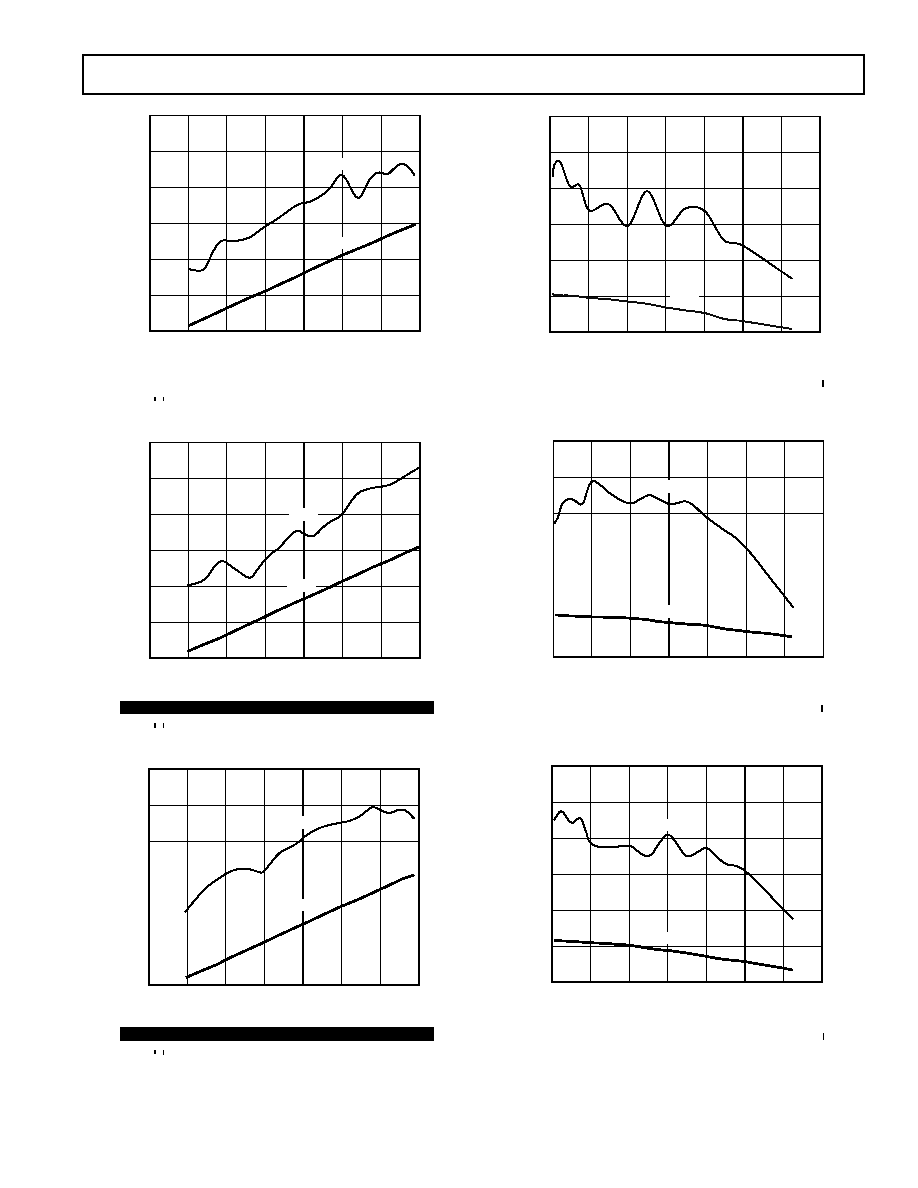
≠120
10
15
20
25
30
5
0
≠100
≠80
≠60
≠40
≠20
0
SECOND
HARMONIC
FREQUENCY ≠ MHz
CROSSTALK
MAGNITUDE ≠ dBFS
THIRD
HARMONIC
TPC 1. Single-Tone FFT of Channel A Digitizing
f
IN
= 12.5 MHz while Channel B is Digitizing f
IN
= 10 MHz
TPC 2. Single-Tone FFT of Channel A Digitizing
f
IN
= 70 MHz while Channel B is Digitizing f
IN
= 76 MHz
TPC 3. Single-Tone FFT of Channel A Digitizing
f
IN
= 120 MHz while Channel B is Digitizing f
IN
= 126 MHz
ADC SAMPLE RATE ≠ MSPS
90
55
40
SFDR/SNR ≠ dBc
85
80
75
70
65
60
45
50
55
60
65
95
100
SNR
SFDR
50
TPC 4. AD9238-65 Single-Tone SNR/SFDR vs. FS with
f
IN
= 32.5 MHz
ADC SAMPLE RATE ≠ MSPS
90
55
40
SFDR/SNR ≠ dBc
85
80
75
70
65
60
95
100
SNR
SFDR
50
35
30
25
20
SNR
SNR
TPC 5. AD9238-40 Single-Tone SNR/SFDR vs. FS with
f
IN
= 20 MHz
TPC 6. AD9238-20 Single-Tone SNR/SFDR vs. FS with
f
IN
= 10 MHz
REV. A
REV. A
AD9238
≠9≠
INPUT AMPLITUDE ≠ dBFS
90
SFDR/SNR ≠ dBc
80
70
60
100
SNR
SFDR
50
≠35
SNR
SNR
40
≠30
≠25
≠20
≠15
≠10
≠5
0
TPC 7. AD9238-65 Single-Tone SNR/SFDR vs. AIN
with f
IN
with f
with f = 32.5 MHz
IN
IN
INPUT AMPLITUDE ≠ dBFS
90
SFDR/SNR ≠ dBc
80
70
60
100
SNR
SFDR
50
≠35
SNR
SNR
40
≠30
≠25
≠20
≠15
≠10
≠5
0
with f
IN
with f
with f = 20 MHz
IN
IN
INPUT AMPLITUDE ≠ dBFS
90
SFDR/SNR ≠ dBc
80
70
60
100
SNR
SFDR
50
≠35
SNR
SNR
40
≠30
≠25
≠20
≠15
≠10
≠5
0
with f
IN
with f
with f = 10 MHz
IN
IN
INPUT FREQUENCY ≠ MHz
90
SFDR/SNR ≠ dBc
85
80
75
95
SNR
SFDR
70
0
SNR
65
20
40
60
80
100
120
140
TPC 10. AD9238-65 Single-Tone SNR/SFDR vs. f
IN
TPC 10. AD9238-65 Single-Tone SNR/SFDR vs. f
TPC 10. AD9238-65 Single-Tone SNR/SFDR vs. f
90
85
80
75
95
SNR
SFDR
70
0
SNR
SNR
65
20
40
60
80
100
120
140
INPUT FREQUENCY ≠ MHz
SFDR/SNR ≠ dBc
TPC 11. AD9238-40 Single-Tone SNR/SFDR vs. f
IN
TPC 11. AD9238-40 Single-Tone SNR/SFDR vs. f
TPC 11. AD9238-40 Single-Tone SNR/SFDR vs. f
90
85
80
75
95
SNR
SFDR
70
0
SNR
SNR
65
20
40
60
80
100
120
140
INPUT FREQUENCY ≠ MHz
SFDR/SNR ≠ dBc
TPC 12. AD9238-20 Single-Tone SNR/SFDR vs. f
IN
TPC 12. AD9238-20 Single-Tone SNR/SFDR vs. f
TPC 12. AD9238-20 Single-Tone SNR/SFDR vs. f
REV. A
AD9238
≠10≠
AD9238
≠11≠
≠120
10
MAGNITUDE ≠ dBFS
15
20
25
30
5
0
≠100
≠80
≠60
≠40
≠20
0
FREQUENCY ≠ MHz
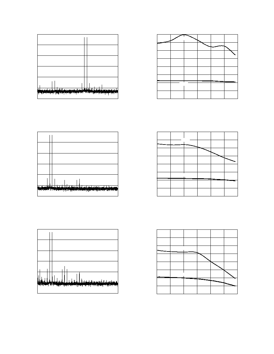
TPC 13. Dual-Tone FFT with f
IN
1 = 45 MHz and
f
IN
2 = 46 MHz
≠120
10
15
20
25
30
5
0
≠100
≠80
≠60
≠40
≠20
0
MAGNITUDE ≠ dBFS
FREQUENCY ≠ MHz
TPC 14. Dual-Tone FFT with f
IN
1 = 70 MHz and
f
IN
2 = 71 MHz
≠120
10
15
20
25
30
5
0
≠100
≠80
≠60
≠40
≠20
0
MAGNITUDE ≠ dBFS
FREQUENCY ≠ MHz
TPC 15. Dual-Tone FFT with f
IN
1 = 200 MHz and
f
IN
2 = 201 MHz
INPUT AMPLITUDE ≠ dBFS
95
SFDR/SNR ≠ dBFS
90
85
80
100
SNR
SFDR
75
≠24
SNR
SNR
70
≠21
≠18
≠15
≠12
≠9
≠6
65
60
TPC 16. Dual-Tone SNR/SFDR vs. AIN with
f
IN
1 = 45 MHz and f
IN
2 = 46 MHz
INPUT AMPLITUDE ≠ dBFS
95
SFDR/SNR ≠ dBFS
90
85
80
100
SNR
SFDR
75
≠24
SNR
SNR
70
≠21
≠18
≠15
≠12
≠9
≠6
65
60
TPC 17. Dual-Tone SNR/SFDR vs. AIN with
f
IN
1 = 70 MHz and f
IN
2 = 71 MHz
INPUT AMPLITUDE ≠ dBFS
95
SFDR/SNR ≠ dBFS
90
85
80
100
SNR
SFDR
75
≠24
SNR
70
≠21
≠18
≠15
≠12
≠9
≠6
65
60
TPC 18. Dual-Tone SNR/SFDR vs. AIN with
f
IN
1 = 200 MHz and f
IN
2 = 201 MHz
REV. A
REV. A
AD9238
≠10≠
AD9238
≠11≠
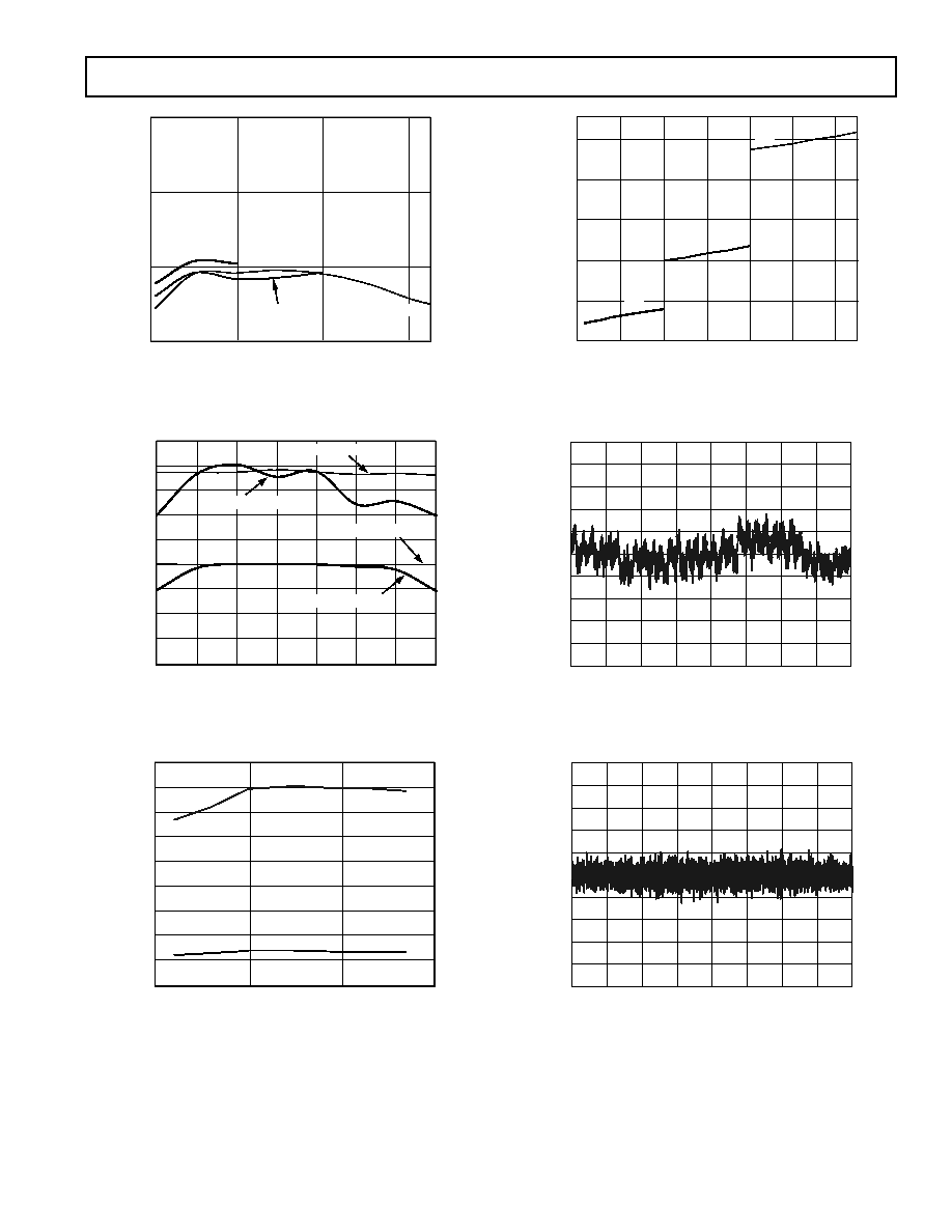
CLOCK FREQUENCY
SINAD ≠ dBc
72
70
74
0
68
20
40
60
SINAD ≠65
SINAD ≠40
SINAD ≠20
12.0
11.5
11.0
TPC 19. SINAD vs. FS with Nyquist Input
DUTY CYCLE ≠ %
85
SINAD/SFDR ≠ dBc
80
75
70
95
65
30
60
40
45
50
55
60
65
55
50
DCS ON ≠ SINAD
DCS ON ≠ SFDR
DCS OFF ≠ SINAD
DCS OFF ≠ SFDR
90
35
TPC 20. SINAD/SFDR vs. Clock Duty Cycle
TEMPERATURE ≠ C
80
SINAD/SFDR ≠ dB
78
76
74
84
72
≠50
70
0
50
100
68
66
SINAD
SFDR
82
TPC 21. SINAD/SFDR vs. Temperature with f
IN
= 32.5 MHz
SAMPLE RATE ≠ MSPS
500
AVDD POWER ≠ mW
400
300
200
600
100
0
10
20
30
40
50
60
≠65
≠40
≠20
TPC 22. Analog Power Consumption vs. FS
CODE
0.6
≠0.8
INL ≠ LSB
0.4
0.2
0
≠0.2
≠0.4
≠0.6
0.8
1.0
≠1.0
1500
1000
500
0
2000
2500
3000
3500
4000
TPC 23. AD9238-65 Typical INL
CODE
0.6
≠0.8
DNL ≠ LSB
0.4
0.2
0
≠0.2
≠0.4
≠0.6
0.8
1.0
≠1.0
1500
1000
500
0
2000
2500
3000
3500
4000
TPC 24. AD9238-65 Typical DNL
REV. A
REV. A
AD9238
≠12≠
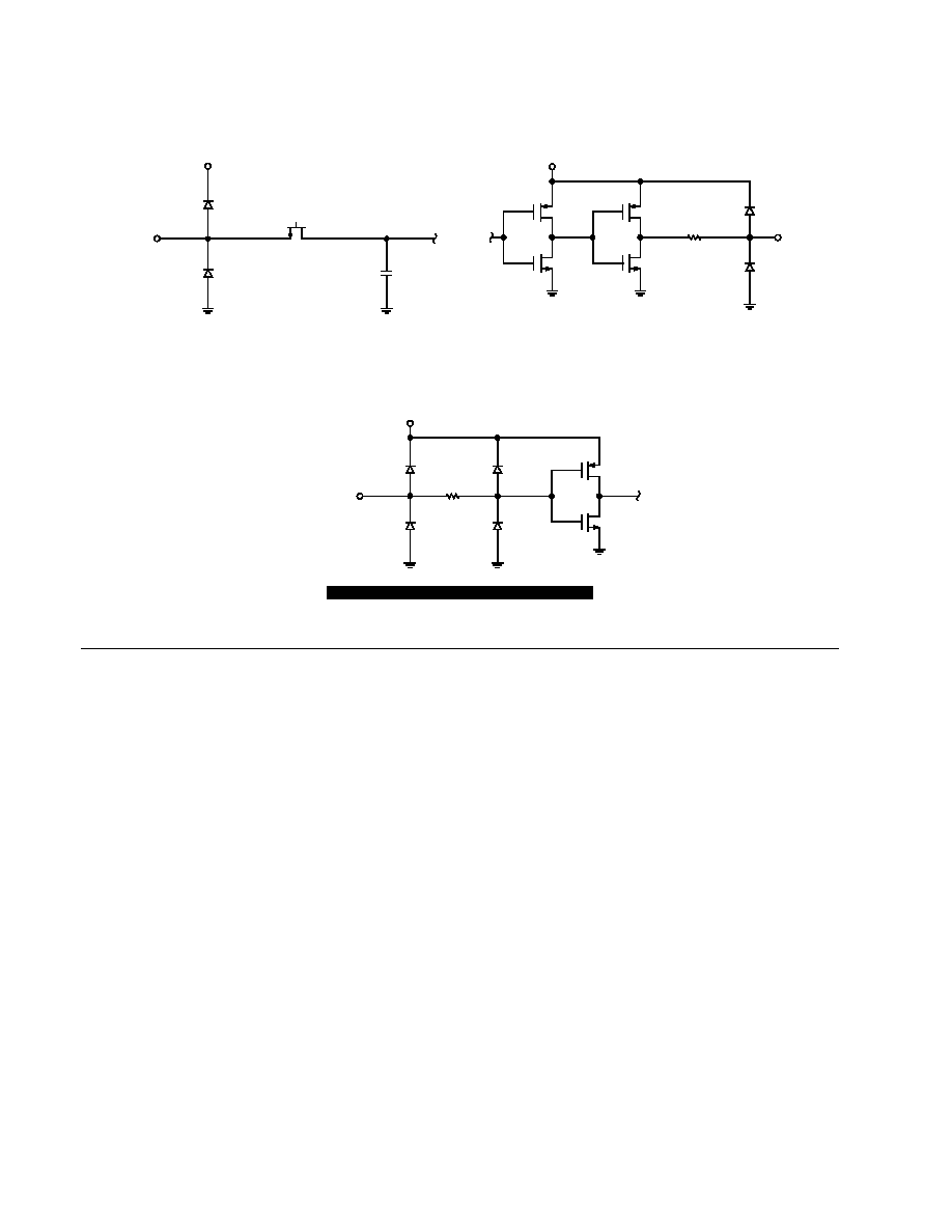
Equivalent Circuits
AVDD
VIN+_A, VIN≠_A,
VIN+_B, VIN≠_B,
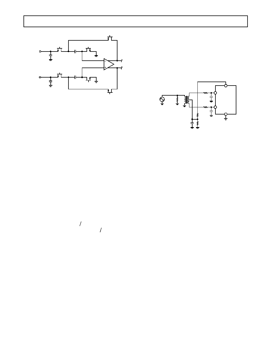
Figure 2. Equivalent Analog Input Circuit
Figure 3. Equivalent Digital Output Circuit
AVDD
CLK_A, CLK_B
DCS, DFS,
MUX_SELECT
SHARED_REF
THEORY OF OPERATION
The AD9238 consists of two high performance analog-to-digital
converters (ADCs) that are based on the AD9235 converter core.
The dual ADC paths are independent, except for a shared internal
band gap reference source, V
REF
. Each of the ADC's paths consists
of a proprietary front end sample-and-hold amplifi er (SHA)
followed by a pipelined switched capacitor ADC. The pipelined
ADC is divided into three sections, consisting of a 4-bit fi rst stage
followed by eight 1.5-bit stages and a fi nal 3-bit fl ash. Each stage
provides suffi cient overlap to correct for fl ash errors in the preced-
ing stages. The quantized outputs from each stage are combined
through the digital correction logic block into a fi nal 12-bit result.
The pipelined architecture permits the fi rst stage to operate on a
new input sample, while the remaining stages operate on preceding
samples. Sampling occurs on the rising edge of the respective clock.
Each stage of the pipeline, excluding the last, consists of a low
resolution fl ash ADC and a residual multiplier to drive the next
stage of the pipeline. The residual multiplier uses the fl ash ADC
output to control a switched capacitor digital-to-analog converter
(DAC) of the same resolution. The DAC output is subtracted from
the stage's input signal and the residual is amplifi ed (multiplied)
to drive the next pipeline stage. The residual multiplier stage is
also called a multiplying DAC (MDAC). One bit of redundancy
is used in each one of the stages to facilitate digital correction of
fl ash errors. The last stage simply consists of a fl ash ADC.
The input stage contains a differential SHA that can be confi g-
ured as ac- or dc-coupled in differential or single-ended modes.
The output-staging block aligns the data, carries out the error
correction, and passes the data to the output buffers. The output
buffers are powered from a separate supply, allowing adjustment
of the output voltage swing.
ANALOG INPUT
The analog input to the AD9238 is a differential switched capacitor,
SHA, that has been designed for optimum performance while
processing a differential input signal. The SHA input accepts inputs
over a wide common-mode range. An input common-mode voltage
of midsupply is recommended to maintain optimal performance.
The SHA input is a differential switched capacitor circuit. In
Figure 5, the clock signal alternatively switches the SHA between
sample mode and hold mode. When the SHA is switched into
sample mode, the signal source must be capable of charging the
sample capacitors and settling within one-half of a clock cycle. A
small resistor in series with each input can help reduce the peak
transient current required from the output stage of the driving
source. Also, a small shunt capacitor can be placed across the inputs
to provide dynamic charging currents. This passive network will
create a low-pass fi lter at the ADC's input; therefore, the precise
values are dependant on the application. In IF undersampling
applications, any shunt capacitors should be removed. In combi-
nation with the driving source impedance, they would limit the
input bandwidth. For best dynamic performance, the source
impedances driving VIN+ and VIN≠ should be matched such that
common-mode settling errors are symmetrical. These errors will
be reduced by the common-mode rejection of the ADC.
REV. A
AD9238
≠13≠
5pF
5pF
T
T
VIN+
VIN≠
C
PAR
T
T
H
H
C
PAR
Figure 5. Switched Capacitor Input
An internal differential reference buffer creates positive and nega-
tive reference voltages, REFT and REFB, respectively, that defi ne
the span of the ADC core. The output common-mode of the
reference buffer is set to midsupply, and the REFT and REFB
voltages and span are defi ned as follows:
REFT
/
AVDD V
REFB
/
AVDD V
Span
REFT REFB
V
REF
REF
REF
=
+
(
)
=
-
(
)
= ◊
-
(
)
= ◊
1 2
1 2
2
2
It can be seen from the equations above that the REFT and REFB
voltages are symmetrical about the midsupply voltage and, by
defi nition, the input span is twice the value of the V
REF
voltage.
The internal voltage reference can be pin-strapped to fi xed values
of 0.5 V or 1.0 V, or adjusted within the same range as discussed
in the Internal Reference Connection section. Maximum SNR
performance will be achieved with the AD9238 set to the largest
input span of 2 V p-p. The relative SNR degradation will be 3 dB
when changing from 2 V p-p mode to 1 V p-p mode.
The SHA may be driven from a source that keeps the signal
peaks within the allowable range for the selected reference volt-
age. The minimum and maximum common-mode input levels
are defi ned as follows:
VCM
V
VCM
(AVDD V
)
MIN
REF
MAX
REF
=
=
+
2
2
The minimum common-mode input level allows the AD9238
to accommodate ground-referenced inputs. Although optimum
performance is achieved with a differential input, a single-ended
source may be driven into VIN+ or VIN≠. In this confi guration,
one input will accept the signal, while the opposite input should
be set to midscale by connecting it to an appropriate reference.
For example, a 2 V p-p signal may be applied to VIN+ while a
1 V reference is applied to VIN≠. The AD9238 will then accept
an input signal varying between 2 V and 0 V. In the single-ended
confi guration, distortion performance may degrade signifi cantly
as compared to the differential case. However, the effect will be
less noticeable at lower input frequencies and in the lower speed
grade models (AD9238-40 and AD9238-20).
Differential Input Confi gurations
As previously detailed, optimum performance will be achieved
while driving the AD9238 in a differential input confi guration.
For baseband applications, the AD8138 differential driver pro-
vides excellent performance and a fl exible interface to the ADC.
The output common-mode voltage of the AD8138 is easily set to
AVDD/2, and the driver can be confi gured in a Sallen-Key fi lter
topology to provide band limiting of the input signal.
At input frequencies in the second Nyquist zone and above, the
performance of most amplifi ers will not be adequate to achieve
the true performance of the AD9238. This is especially true in
IF undersampling applications where frequencies in the 70 MHz
to 200 MHz range are being sampled. For these applications,
differential transformer coupling is the recommended input con-
fi guration, as shown in Figure 6.
AD9238
VINA
VINB
AVDD
AGND
2V p-p
50
50
10pF
10pF
49.9
1k
1k
0.1F
Figure 6. Differential Transformer Coupling
The signal characteristics must be considered when selecting a
transformer. Most RF transformers will saturate at frequencies
below a few MHz, and excessive signal power can also cause core
saturation, which leads to distortion.
Single-Ended Input Confi guration
A single-ended input may provide adequate performance in
cost-sensitive applications. In this confi guration, there will be a
degradation in SFDR and in distortion performance due to the
large input common-mode swing. However, if the source imped-
ances on each input are matched, there should be little effect on
SNR performance.
CLOCK INPUT AND CONSIDERATIONS
Typical high speed ADCs use both clock edges to generate a
variety of internal timing signals, and as a result may be sensitive
to clock duty cycle. Commonly, a 5% tolerance is required on the
clock duty cycle to maintain dynamic performance characteristics.
The AD9238 provides separate clock inputs for each channel. The
optimum performance is achieved with the clocks operated at the
same frequency and phase. Clocking the channels asynchronously
may degrade performance signifi cantly. In some applications, it is
desirable to skew the clock timing of adjacent channels. The AD9238's
separate clock inputs allow for clock timing skew (typically ±1 ns)
between the channels without signifi cant performance degradation.
The AD9238-65 contains two clock duty cycle stabilizers, one for
each converter, that retime the nonsampling edge, providing an
internal clock with a nominal 50% duty cycle (DCS is not avail-
able on the ≠40 MSPS or ≠20 MSPS versions). Input clock rates
of over 40 MHz can use the DCS so that a wide range of input
clock duty cycles can be accommodated. Maintaining a 50% duty
cycle clock is particularly important in high speed applications,
when proper track-and-hold times for the converter are required
to maintain high performance. The DCS can be enabled by tying
the DCS pin high.
The duty cycle stabilizer utilizes a delay locked loop to create the
nonsampling edge. As a result, any changes to the sampling fre-
quency will require approximately 2 µs to 3 µs to allow the DLL
to acquire and settle to the new rate.
REV. A
AD9238
≠14≠
High speed, high resolution ADCs are sensitive to the quality of
the clock input. The degradation in SNR at a given full-scale input
frequency (f
INPUT
frequency (f
frequency (f
) due only to aperture jitter (t
J
) due only to aperture jitter (t
) due only to aperture jitter (t ) can be calculated
with the following equation:
SNR degradation
/
f
t
INPUT
=
◊
◊ ◊
◊
[
]
20
10 1 2
log
p
J
In the equation, the rms aperture jitter, t
J
t
t , represents the root-sum-
square of all jitter sources, which includes the clock input, analog
input signal, and ADC aperture jitter specifi cation. Undersampling
applications are particularly sensitive to jitter.
For optimal performance, especially in cases where aperture jitter
may affect the dynamic range of the AD9238, it is important to
minimize input clock jitter. The clock input circuitry should use
stable references, for example using analog power and ground
planes to generate the valid high and low digital levels for the
AD9238 clock input. Power supplies for clock drivers should be sep-
arated from the ADC output driver supplies to avoid modulating
the clock signal with digital noise. Low jitter crystal controlled
oscillators make the best clock sources. If the clock is generated
from another type of source (by gating, dividing, or other methods),
it should be retimed by the original clock at the last step.
POWER DISSIPATION AND STANDBY MODE
The power dissipated by the AD9238 is proportional to its
sampling rates. The digital (DRVDD) power dissipation is deter-
mined primarily by the strength of the digital drivers and the load
on each output bit. The digital drive current can be calculated by
I
V
C
f
N
DRVDD
DRVDD
LOAD
CLOCK
=
◊
◊
◊
where N is the number of bits changing and
N
N
C
LOAD
C
C
is the average
LOAD
LOAD
load on the digital pins that changed.
The analog circuitry is optimally biased so that each speed grade
provides excellent performance while affording reduced power
consumption. Each speed grade dissipates a baseline power at low
sample rates that increases with clock frequency.
Either channel of the AD9238 can be placed into standby mode
independently by asserting the PWDN_A or PDWN_B pins.
It is recommended that the input clock(s) and analog input(s)
remain static during either independent or total standby, which
will result in a typical power consumption of 1 mW for the ADC.
Note that if DCS is enabled, it is mandatory to disable the clock
of an independently powered-down channel. Otherwise, sig-
nifi cant distortion will result on the active channel. If the clock
inputs remain active while in total standby mode, typical power
dissipation of 12 mW will result.
The minimum standby power is achieved when both channels are
placed into full power-down mode (PDWN_A = PDWN_B =
HI). Under this condition, the internal references are powered
down. When either or both of the channel paths are enabled after a
power-down, the wake-up time will be directly related to the
recharging of the REFT and REFB decoupling capacitors and to
the duration of the power-down. Typically, it takes approximately
5 ms to restore full operation with fully discharged 0.1 µF and
10 µF decoupling capacitors on REFT and REFB.
A single channel can be powered down for moderate power savings.
The powered-down channel shuts down internal circuits, but both
the reference buffers and shared reference remain powered. Because
the buffer and voltage reference remain powered, the wake-up
time is reduced to several clock cycles.
DIGITAL OUTPUTS
The AD9238 output drivers can be confi gured to interface with
2.5 V or 3.3 V logic families by matching DRVDD to the digital
supply of the interfaced logic. The output drivers are sized to pro-
vide suffi cient output current to drive a wide variety of logic families.
However, large drive currents tend to cause current glitches on
the supplies that may affect converter performance. Applications
requiring the ADC to drive large capacitive loads or large fan-outs
may require external buffers or latches.
The data format can be selected for either offset binary or twos
complement. This is discussed later in the Data Format section.
TIMING
The AD9238 provides latched data outputs with a pipeline delay
of seven clock cycles. Data outputs are available one propaga-
tion delay (t
PD
) after the rising edge of the clock signal. Refer to
Figure 1 for a detailed timing diagram.
B
≠8
A
≠7
B
≠7
A
≠6
B
≠6
A
≠5
B
≠5
A
≠4
B
≠4
A
≠3
B
≠3
A
≠2
B
≠2
A
≠1
B
≠1
A
0
B
0
A
1
A
≠1
A
0
A
1
A
2
A
3
A
4
A
5
A
6
A
7
A
8
B
≠1
B
0
B
1
B
2
B
3
B
4
B
5
B
6
B
7
B
8
ANALOG INPUT
ADC A
ANALOG INPUT
ADC B
CLK_A = CLK_B =
MUX_SELECT
D0_A
≠D11_A
t
ODF
t
ODR
Figure 7. Example of Multiplexed Data Format Using the Channel A Output and the Same Clock Tied to CLK_A,
CLK_B, and MUX_SELECT
REV. A
AD9238
≠15≠
The internal duty cycle stabilizer can be enabled on the AD9238-65
using the DCS pin. This provides a stable 50% duty cycle to
internal circuits.
The length of the output data lines and loads placed on them should
be minimized to reduce transients within the AD9238. These
transients can detract from the converter's dynamic performance.
The lowest typical conversion rate of the AD9238 is 1 MSPS. At
clock rates below 1 MSPS, dynamic performance may degrade.
DATA FORMAT
The AD9238 data output format can be confi gured for either
twos complement or offset binary. This is controlled by the Data
Format Select pin (DFS). Connecting DFS to AGND will pro-
duce offset binary output data. Conversely, connecting DFS to
AVDD will format the output data as twos complement.
The output data from the dual A/D converters can be multiplexed
onto a single 12-bit output bus. The multiplexing is accomplished
by toggling the MUX_SELECT bit, which directs channel data
to the same or opposite channel data port. When MUX_SELECT
is logic high, the Channel A data is directed to Channel A output
bus, and Channel B data is directed to the Channel B output bus.
When MUX_SELECT is logic low, the channel data is reversed, i.e.,
Channel A data is directed to the Channel B output bus and
Channel B data is directed to the Channel A output bus. By
toggling the MUX_SELECT bit, multiplexed data is available
on either of the output data ports.
If the ADCs are run with synchronized timing, this same clock can
be applied to the MUX_SELECT bit. After the MUX_SELECT
rising edge, either data port will have the data for its respective
channel; after the falling edge, the alternate channel's data will be
placed on the bus. Typically, the other unused bus would be
disabled by setting the appropriate OEB high to reduce power
consumption and noise. Figure 7 shows an example of multiplex
mode. When multiplexing data, the data rate is two times the
sample rate. Note that both channels must remain active in this
mode and that each channel's power-down pin must remain low.
VOLTAGE REFERENCE
A stable and accurate 0.5 V voltage reference is built into the
AD9238. The input range can be adjusted by varying the reference
voltage applied to the AD9238, using either the internal reference
with different external resistor confi gurations or an externally
applied reference voltage. The input span of the ADC tracks refer-
ence voltage changes linearly.
If the ADC is being driven differentially through a transformer,
the reference voltage can be used to bias the center tap (common-
mode voltage).
The Shared Reference mode allows the user to connect the refer-
ences from the dual ADCs together externally for superior gain
and offset matching performance. If the ADCs are to function
independently, the reference decoupling can be treated inde-
pendently and can provide superior isolation between the dual
channels. To enable Shared Reference mode, the SHARED_REF
pin must be tied high and external differential references must
be externally shorted. (REFT_A must be externally shorted to
REFT_B and REFB_A must be shorted to REFB_B.)
Internal Reference Connection
A comparator within the AD9238 detects the potential at the
SENSE pin and confi gures the reference into four possible states,
which are summarized in Table I. If SENSE is grounded, the refer-
ence amplifi er switch is connected to the internal resistor divider
(see Figure 8), setting V
REF
to 1 V. Connecting the SENSE pin to
V
REF
switches the reference amplifi er output to the SENSE pin,
completing the loop and providing a 0.5 V reference output. If a
resistor divider is connected as shown in Figure 9, the switch will
again be set to the SENSE pin. This will put the reference ampli-
fi er in a noninverting mode with the V
REF
output defi ned as follows:
V
.
(
R R )
REF
=
◊ +
0 5
1
2
1
In all reference confi gurations, REFT and REFB drive the ADC
core and establish its input span. The input range of the ADC
always equals twice the voltage at the reference pin for either an
internal or an external reference.
VIN+
VIN≠
10F
10F
0.1F
0.1F
REFT
ADC
CORE
SELECT
LOGIC
SENSE
0.1F
0.5V
AD9238
REFB
0.1F
V
REF
Figure 8. Internal Reference Confi guration
Table I. Reference Confi guration Summary
Resulting Differential
Selected Mode SENSE Voltage Resulting V
REF
(V)
Span (V p-p)
External Reference AVDD N/A
2 External Reference
Internal Fixed Reference V
REF
0.5
1.0
Programmable Reference 0.2 V to V
REF
0.5 (1 + R2/R1)
2 V
REF
(See Figure 9)
Internal Fixed Reference AGND to 0.2 V 1.0
2.0
REV. A
AD9238
≠16≠
External Reference Operation
The use of an external reference may be necessary to enhance the
gain accuracy of the ADC or to improve thermal drift character-
istics. When multiple ADCs track one another, a single reference
(internal or external) may be necessary to reduce gain matching
errors to an acceptable level. A high precision external reference
may also be selected to provide lower gain and offset temperature
drift. Figure 10 shows the typical drift characteristics of the inter-
nal reference in both 1 V and 0.5 V modes.
When the SENSE pin is tied to AVDD, the internal reference will
be disabled, allowing the use of an external reference. An internal
reference buffer will load the external reference with an equiva-
lent 7 k load. The internal buffer will still generate the positive
and negative full-scale references, REFT and REFB, for the ADC
core. The input span will always be twice the value of the refer-
ence voltage; therefore, the external reference must be limited to
a maximum of 1 V.
If the internal reference of the AD9238 is used to drive multiple
converters to improve gain matching, the loading of the reference
by the other converters must be considered. Figure 11 depicts
how the internal reference voltage is affected by loading.
VIN+
VIN≠
V
REF
10F
10F
10F
0.1F
0.1F
REFT
ADC
CORE
SELECT
LOGIC
SENSE
0.5V
AD9238
REFB
0.1F
R1
R2
Figure 9. Programmable Reference Confi guration
TEMPERATURE ≠ C
0.2
V
REF
ERROR ≠
%
1.2
1.0
0.8
0.6
0.4
0
≠40 ≠30 ≠20 ≠10 0
10
20
30 40
50
60
70
80
V
REF
= 1V
V
REF
= 0.5V
Figure 10. Typical V
REF
Figure 10. Typical V
Figure 10. Typical V
Drift
REF
REF
LOAD ≠ mA
≠0.20
ERROR ≠
%
0.05
0
≠0.05
≠0.10
≠0.15
≠0.25
0
0.5
1.0
1.5
2.0
2.5
3.0
0.5V ERROR
1V ERROR
Figure 11. V
REF
Figure 11. V
Figure 11. V
Accuracy vs. Load
REF
REF
REV. A
AD9238
≠17≠
B
A
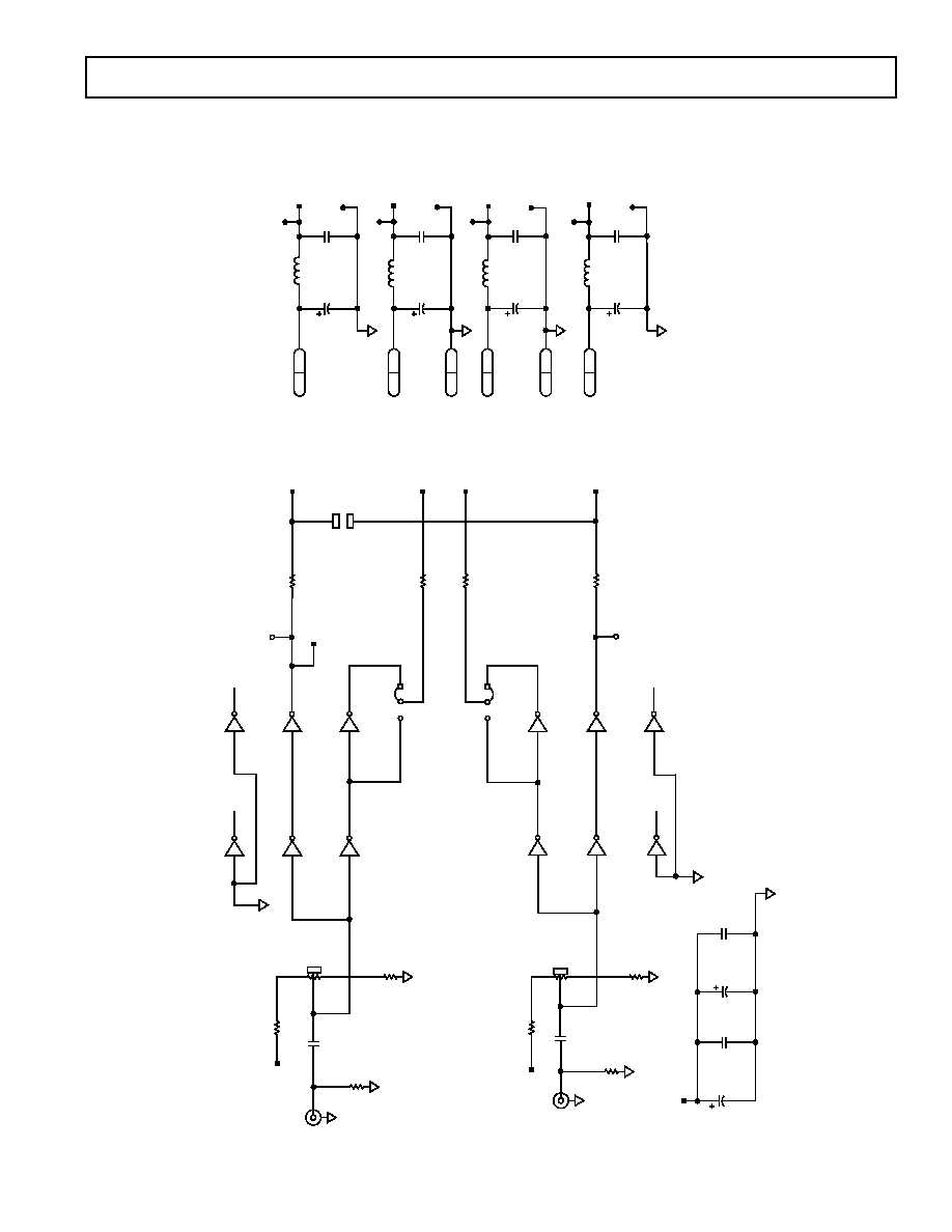
Figure 12. Evaluation Board Schematic
EVALUATION BOARD DIAGRAMS
REV. A
AD9238
≠18≠
A
V
D
D
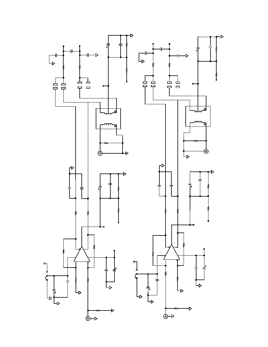
Figure 13. Evaluation Board Schematic (continued)
REV. A
AD9238
≠19≠
0.01
F
D
U
T
A
V
D
D
AVDD
AVDD
R36 10k
JP6
R41 5k
5k
R51
A
V
D
D
C1 10
F
6.3V
A
V
D
D
R44 5k
C34
6.3V
10
F
VIN+_B
VIN≠_B
V
I
N
≠
_
A
O
T
R
A
D
A
1
3
D
A
1
2
D
A
1
1
D
A
1
0
D
A
9
D
A
8
D
A
7
D
A
6
D
A
5
D
A
4
D
A
3
D
A
2
D
A
1
OTRB
D
B
1
3
D
B
1
2
D
B
1
1
D
B
1
0
D
B
9
D
B
7
D
B
6
D
B
5
D
B
4
D
B
3
D
B
2
D
B
1
D1
2
1
D
U
T
A
V
D
D
D
U
T
D
R
V
D
D
10k
R4
D
B
0
D
B
8
D
A
0
A
G
N
D
;
4
A
V
D
D
;
8
U4
2
1
3
A
G
N
D
;
4
A
V
D
D
;
8
U4
OUT
5
7
6
V
I
N
+
_
A
C35 0.1
F
C37
0.1
F
0.1
F
C38
0.1
F
C36
5.49k
R3
5k
R5
0.1
F
C30
C29
0.1
F
0.1
F
R43 5k
R6 5k
R38 5k
U1
64
63
62
61
60
59
58
57
56
55
54
53
52
51
50
49
3
2
3
1
3
0
2
9
2
8
2
7
2
6
2
5
48
2
4
1
33
34
35
36
37
38
39
40
41
42
43
44
45
46
47
2
3
2
2
2
1
2
0
1
9
1
8
1
7
1
6
1
5
1
4
1
3
1
2
1
1
1
0
9
8
7
6
5
4
3
2
C12
TP9 WH
T
JP7
A
V
D
D
C
L
K
A
O
DUTCLKB
D
U
T
C
L
K
A
R37 10k
0.01
F
C52
1.2V
A
D
8
2
2
A
D
8
2
2
A
D
9
2
3
8
V
I
N
+
_
A
V
I
N
≠
_
A
A
V
S
S
2
A
V
D
D
2
R
E
F
T
_
A
R
E
F
B
_
A
VREF
SENSE
REFB_B
REFT_B
A
V
D
D
3
A
V
S
S
3
VIN≠_B
VIN+_B
A
V
S
S
4
A
V
D
D
4
CLK_B
DUTYEN
DFS
PDWN_B
D
N
C
D
3
_
A
D
2
_
A
D
1
_
A
D
0
_
A
D
N
C
D
N
C
D
R
V
D
D
2
D
R
V
S
S
2
OTR_B
(
M
S
B
)
D
1
1
_
B
D
1
0
_
B
D
9
_
B
D
8
_
B
D
7
_
B
D
6
_
B
A
V
S
S
1
D
N
C
D
4
_
A
D
0
_
B
D
1
_
B
D
2
_
B
D
R
V
S
S
1
D
R
V
D
D
1
D
3
_
B
D
4
_
B
D
5
_
B
D
5
_
A
D
6
_
A
D
7
_
A
D
R
V
D
D
3
D
R
V
S
S
3
D
8
_
A
D
9
_
A
D
1
0
_
A
(
M
S
B
)
D
1
1
_
A
O
T
R
_
A
P
D
W
N
_
A
MUXSELECT
S
H
A
R
E
D
R
E
F
C
L
K
_
A
A
V
D
D
1
O
E
B
_
A
O
E
B
_
B
C31
JP11
JP12
JP2
JP3
JP4
JP1
10
F
6.3V
C57
JP5
C32 0.1
F
0.1
F
C39
0.1
F
C40
10
F
6.3V
C33
C
W
JP35
JP8
C24 0.1
F
C25 0.001
F
0.1
F
C26
0.001
F
C13
C14 0.1
F
C11 10
F
6.3V
0.001
F
C23
JP23
JP27
JP29
JP28
JP10
0.1
F
C22
C15 0.001
F
C17 0.1
F
0.001
F
C18
0.001
F
C19
C20 0.1
F
C21 0.001
F
0.1
F
C16
JP9
C2 10
F
6.3V
A
V
D
D
+
I
N
≠
I
N
OUT
+
I
N
≠
I
N
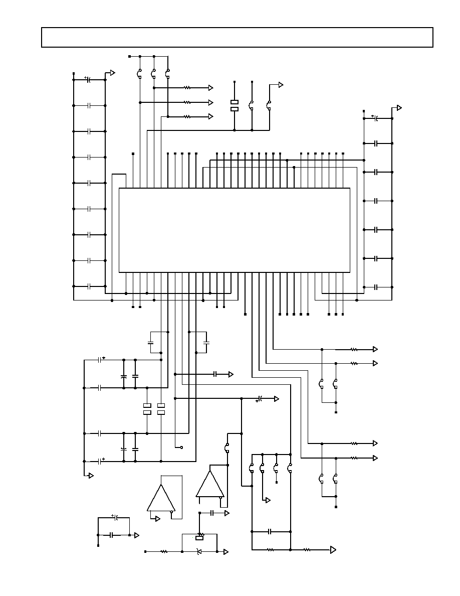
Figure 14. Evaluation Board Schematic (continued)
REV. A
AD9238
≠20≠
4
2
2
RP11
DVDD
U10
18
2
11
12
13
14
15
16
17
20
10
19
1
9
8
7
6
5
4
3
U7
3
4
5
6
7
8
9
1
19
10
20
17
16
15
14
13
12
11
2
DA13
DA12
DA11
DA10
DA9
DA8
DA7
DA6
DA5
DA4
DA3
DA2
DA1
RP10
4
RP10
6
3
RP4
6
3
RP4
2
7
RP3
4
5
RP3
6
3
RP3
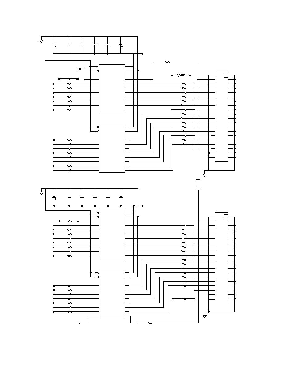
Figure 15. Evaluation Board Schematic (continued)
REV. A
AD9238
≠20≠
AD9238
≠21≠
Figure 17. PCB Bottom Layer
Figure 16. PCB Top Layer
REV. A
REV. A
AD9238
≠22≠
AD9238
≠23≠
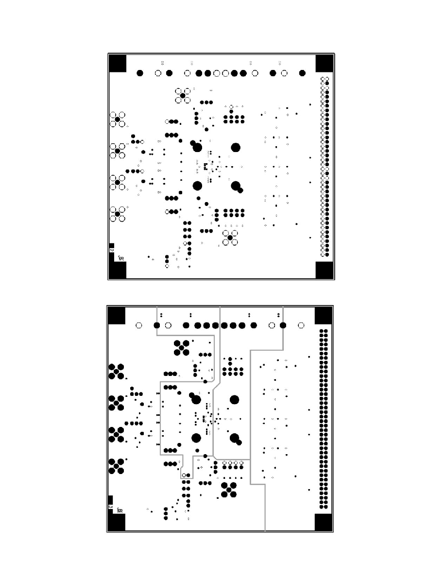
Figure 19. PCB Split Power Plane
Figure 18. PCB Ground Plane
REV. A
REV. A
AD9238
≠22≠
AD9238
≠23≠
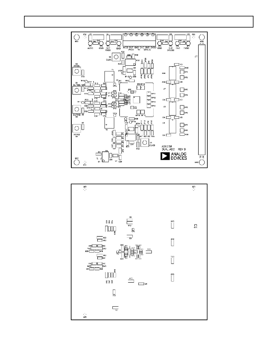
Figure 21. PCB Bottom Silkscreen
Figure 20. PCB Top Silkscreen
REV. A
REV. A
C02640≠0≠9/03(A)
≠24≠
AD9238
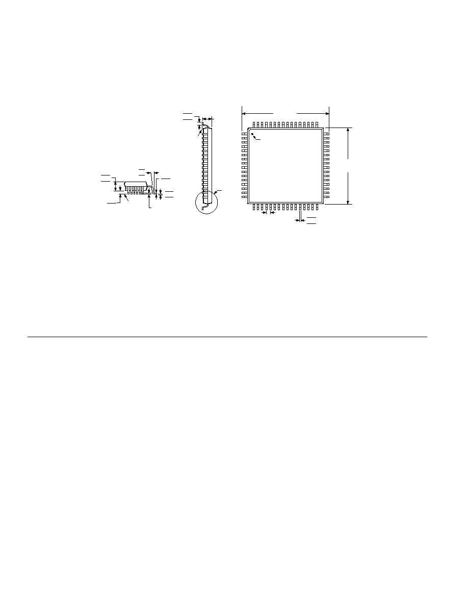
OUTLINE DIMENSIONS
64-Lead Low Profile Quad Flat Package [LQFP]
(ST-64-1)
Dimensions shown in millimeters
TOP VIEW
(PINS DOWN)
1
16
17
33
32
48
49
64
0.23
0.18
0.13
0.40
BSC
7.00
BSC SQ
1.60
MAX
SEATING
PLANE
0.75
0.60
0.45
VIEW A
9.00 BSC
SQ
0.20
0.09
1.45
1.40
1.35
0.10 MAX
COPLANARITY
VIEW A
ROTATED 90 CCW
SEATING
PLANE
10
6
2
7
3.5
0
0.15
0.05
PIN 1
COMPLIANT TO JEDEC STANDARDS MS-026BBD
Revision History
Location Page
9/03--Data Sheet changed from REV. 0 to REV. A.
Changes to DC SPECIFICATIONS . . . . . . . . . . . . . . . . . . . . . . . . . . . . . . . . . . . . . . . . . . . . . . . . . . . . . . . . . . . . . . . . . . . . . . . . . 2
Changes to SWITCHING SPECIFICATIONS . . . . . . . . . . . . . . . . . . . . . . . . . . . . . . . . . . . . . . . . . . . . . . . . . . . . . . . . . . . . . . . . . 3
Changes to AC SPECIFICATIONS . . . . . . . . . . . . . . . . . . . . . . . . . . . . . . . . . . . . . . . . . . . . . . . . . . . . . . . . . . . . . . . . . . . . . . . . . . 4
Changes to Figure 1 . . . . . . . . . . . . . . . . . . . . . . . . . . . . . . . . . . . . . . . . . . . . . . . . . . . . . . . . . . . . . . . . . . . . . . . . . . . . . . . . . . . . . . 4
Changes to ORDERING GUIDE . . . . . . . . . . . . . . . . . . . . . . . . . . . . . . . . . . . . . . . . . . . . . . . . . . . . . . . . . . . . . . . . . . . . . . . . . . . 5
Changes to TPCs 2, 3, and 6 . . . . . . . . . . . . . . . . . . . . . . . . . . . . . . . . . . . . . . . . . . . . . . . . . . . . . . . . . . . . . . . . . . . . . . . . . . . . . . . . 8
Changes to CLOCK INPUT AND CONSIDERATIONS section . . . . . . . . . . . . . . . . . . . . . . . . . . . . . . . . . . . . . . . . . . . . . . . . . . 13
Added text to DATA FORMAT section . . . . . . . . . . . . . . . . . . . . . . . . . . . . . . . . . . . . . . . . . . . . . . . . . . . . . . . . . . . . . . . . . . . . . . 15
Changes to Figure 9 . . . . . . . . . . . . . . . . . . . . . . . . . . . . . . . . . . . . . . . . . . . . . . . . . . . . . . . . . . . . . . . . . . . . . . . . . . . . . . . . . . . . . 16
Added EVALUATION BOARD DIAGRAMS section . . . . . . . . . . . . . . . . . . . . . . . . . . . . . . . . . . . . . . . . . . . . . . . . . . . . . . . . . . . 17
Updated OUTLINE DIMENSIONS . . . . . . . . . . . . . . . . . . . . . . . . . . . . . . . . . . . . . . . . . . . . . . . . . . . . . . . . . . . . . . . . . . . . . . . . 24
REV. A
Document Outline
- FEATURES
- APPLICATIONS
- FUNCTIONAL BLOCK DIAGRAM
- GENERAL DESCRIPTION
- PRODUCT HIGHLIGHTS
- SPECIFICATIONS
- DC SPECIFICATIONS
- SWITCHING SPECIFICATIONS
- AC SPECIFICATIONS
- ABSOLUTE MAXIMUM RATINGS
- EXPLANATION OF TEST LEVELS
- ORDERING GUIDE
- PIN CONFIGURATION
- PIN FUNCTION DESCRIPTIONS
- TERMINOLOGY
- Typical Performance Characteristics
- Equivalent Circuits
- THEORY OF OPERATION
- ANALOG INPUT
- Differential Input Configurations
- Single-Ended Input Configuration
- CLOCK INPUT AND CONSIDERATIONS
- POWER DISSIPATION AND STANDBY MODE
- DIGITAL OUTPUTS
- TIMING
- DATA FORMAT
- VOLTAGE REFERENCE
- Internal Reference Connection
- External Reference Operation
- EVALUATION BOARD DIAGRAMS
- OUTLINE DIMENSIONS
- Revision History