 | ÐлекÑÑоннÑй компоненÑ: AD9283 | СкаÑаÑÑ:  PDF PDF  ZIP ZIP |
Äîêóìåíòàöèÿ è îïèñàíèÿ www.docs.chipfind.ru
REV. B
Information furnished by Analog Devices is believed to be accurate and
reliable. However, no responsibility is assumed by Analog Devices for its
use, nor for any infringements of patents or other rights of third parties
which may result from its use. No license is granted by implication or
otherwise under any patent or patent rights of Analog Devices.
a
AD9283
One Technology Way, P.O. Box 9106, Norwood, MA 02062-9106, U.S.A.
Tel: 781/329-4700
World Wide Web Site: http://www.analog.com
Fax: 781/326-8703
© Analog Devices, Inc., 1999
8-Bit, 50 MSPS/80 MSPS/100 MSPS
3 V A/D Converter
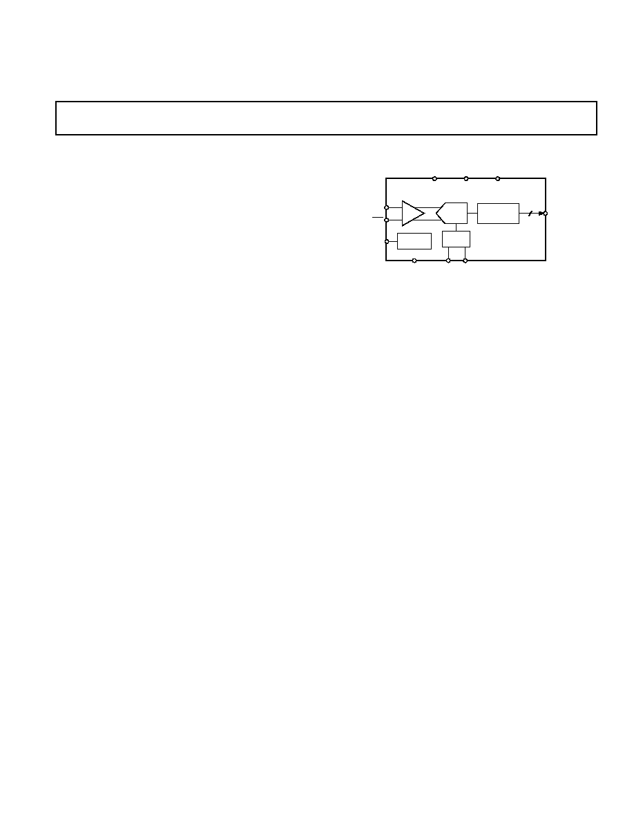
FUNCTIONAL BLOCK DIAGRAM
REF
TIMING
V
D
PWRDWN
V
DD
A
IN
GND
REF
OUT
REF
IN
ADC
OUTPUT
STAGING
ENCODE
AD9283
8
D7D0
T/H
A
IN
FEATURES
8-Bit, 50, 80 and 100 MSPS ADC
Low Power: 90 mW at 100 MSPS
On-Chip Reference and Track/Hold
475 MHz Analog Bandwidth
SNR = 46.5 dB @ 41 MHz at 100 MSPS
1 V p-p Analog Input Range
Single +3.0 V Supply Operation (2.7 V3.6 V)
Power-Down Mode: 4.2 mW
APPLICATIONS
Battery Powered Instruments
Hand-Held Scopemeters
Low Cost Digital Oscilloscopes
GENERAL DESCRIPTION
The AD9283 is an 8-bit monolithic sampling analog-to-digital
converter with an on-chip track-and-hold circuit and is opti-
mized for low cost, low power, small size and ease of use. The
product operates at a 100 MSPS conversion rate, with outstand-
ing dynamic performance over its full operating range.
The ADC requires only a single 3.0 V (2.7 V to 3.6 V) power
supply and an encode clock for full performance operation. No
external reference or driver components are required for many
applications. The digital outputs are TTL/CMOS compatible
and a separate output power supply pin supports interfacing
with 3.3 V or 2.5 V logic.
The encoder input is TTL/CMOS compatible. A power-down
function may be exercised to bring total consumption to
4.2 mW. In power-down mode, the digital outputs are driven
to a high impedance state.
Fabricated on an advanced CMOS process, the AD9283 is
available in a 20-lead surface mount plastic package (SSOP)
specified over the industrial temperature range (40
°
C to +85
°
C).

2
REV. B
AD9283SPECIFICATIONS
(V
DD
= 3.0 V, V
D
= 3.0 V; single-ended input; external reference, unless otherwise noted)
Test
AD9283BRS-100
AD9283BRS-80
AD9283BRS-50
Parameter
Temp
Level
Min
Typ
Max
Min
Typ
Max
Min
Typ
Max
Units
RESOLUTION
8
8
8
Bits
DC ACCURACY
Differential Nonlinearity
+25
°
C
I
±
0.5
+1.25
±
0.5
+1.25
±
0.5
+1.25
LSB
Full
VI
+1.50
+1.50
+1.50
LSB
Integral Nonlinearity
+25
°
C
I
1.25
±
0.75
+1.25
1.25
±
0.75
+1.25
1.25
±
0.75
+1.25
LSB
Full
VI
+2.25
+1.50
+1.50
LSB
No Missing Codes
Full
VI
Guaranteed
Guaranteed
Guaranteed
Gain Error
1
+25
°
C
I
6
±
2.5
+6
6
±
2.5
+6
6
±
2.5
+6
% FS
Full
VI
8
+8
8
+8
8
+8
% FS
Gain Tempco
1
Full
VI
80
80
80
ppm/
°
C
ANALOG INPUT
Input Voltage Range
(With Respect to A
IN
)
Full
V
±
512
±
512
±
512
mV p-p
Common-Mode Voltage
Full
V
±
200
±
200
±
200
mV
Input Offset Voltage
+25
°
C
I
35
±
10
35
35
±
10
35
35
±
10
35
mV
Full
VI
±
40
±
40
±
40
mV
Reference Voltage
Full
VI
1.2
1.25
1.3
1.2
1.25
1.3
1.2
1.25
1.3
V
Reference Tempco
Full
VI
±
130
±
130
±
130
ppm/
°
C
Input Resistance
+25
°
C
I
7
10
13
7
10
13
7
10
13
k
Full
VI
5
16
5
16
5
16
k
Input Capacitance
+25
°
C
V
2
2
2
pF
Full
VI
µ
A
Analog Bandwidth, Full Power
+25
°
C
V
475
475
475
MHz
SWITCHING PERFORMANCE
Maximum Conversion Rate
Full
VI
100
80
50
MSPS
Minimum Conversion Rate
+25
°
C
IV
1
1
1
MSPS
Encode Pulsewidth High (t
EH
)
+25
°
C
IV
4.3
1000
5.0
1000
8.0
1000
ns
Encode Pulsewidth Low (t
EL
)
+25
°
C
IV
4.3
1000
5.0
1000
8.0
1000
ns
Aperture Delay (t
A
)
+25
°
C
V
0
0
0
ns
Aperture Uncertainty (Jitter)
+25
°
C
V
5
5
5
ps rms
Output Valid Time (t
V
)
2
Full
VI
2.0
3.0
2.0
3.0
2.0
3.0
ns
Output Propagation Delay (t
PD
)
2
Full
VI
4.5
7.0
4.5
7.0
4.5
7.0
ns
DIGITAL INPUTS
Logic "1" Voltage
Full
VI
2.0
2.0
2.0
V
Logic "0" Voltage
Full
VI
0.8
0.8
0.8
V
Logic "1" Current
Full
VI
±
1
±
1
±
1
µ
A
Logic "0" Current
Full
VI
±
1
±
1
±
1
µ
A
Input Capacitance
+25
°
C
V
2.0
2.0
2.0
pF
DIGITAL OUTPUTS
Logic "1" Voltage
Full
VI
2.95
2.95
2.95
V
Logic "0" Voltage
Full
VI
0.05
0.05
0.05
V
Output Coding
Offset Binary Code
Offset Binary Code
Offset Binary Code
POWER SUPPLY
Power Dissipation
3, 4
Full
VI
90
120
90
115
80
100
mW
Power-Down Dissipation
Full
VI
4.2
7
4.2
7
4.2
7
mW
Power Supply Rejection Ratio
(PSRR)
+25
°
C
I
18
18
18
mV/V
3
REV. B
AD9283
Test
AD9283BRS-100
AD9283BRS-80
AD9283BRS-50
Parameter
Temp
Level
Min Typ
Max
Min
Typ
Max
Min
Typ
Max
Units
DYNAMIC PERFORMANCE
5
Transient Response
+25
°
C
V
2
2
2
ns
Overvoltage Recovery Time
+25
°
C
V
2
2
2
ns
Signal-to-Noise Ratio (SNR)
(Without Harmonics)
f
IN
= 10.3 MHz
+25
°
C
I
46.5
47
44
47
dB
f
IN
= 27 MHz
+25
°
C
I
46.5
44
47
47
dB
f
IN
= 41 MHz
+25
°
C
I
43.5 46.5
47
dB
f
IN
= 76 MHz
+25
°
C
V
46.0
dB
Signal-to-Noise Ratio (SINAD)
(With Harmonics)
f
IN
= 10.3 MHz
+25
°
C
I
45
47
43.5
46.5
dB
f
IN
= 27 MHz
+25
°
C
I
45.5
43.5
46.5
46
dB
f
IN
= 41 MHz
+25
°
C
I
42.5 45
42
dB
f
IN
= 76 MHz
+25
°
C
V
42.5
dB
Effective Number of Bits
f
IN
= 10.3 MHz
+25
°
C
I
7.3
7.5
7.6
Bits
f
IN
= 27 MHz
+25
°
C
I
7.4
7.5
7.5
Bits
f
IN
= 41 MHz
+25
°
C
I
7.3
7.5
Bits
f
IN
= 76 MHz
+25
°
C
V
6.9
Bits
2nd Harmonic Distortion
f
IN
= 10.3 MHz
+25
°
C
I
57
60
55
60
dBc
f
IN
= 27 MHz
+25
°
C
I
60
55
60
56
dBc
f
IN
= 41 MHz
+25
°
C
I
50
58
55
dBc
f
IN
= 76 MHz
+25
°
C
V
46
dBc
3rd Harmonic Distortion
f
IN
= 10.3 MHz
+25
°
C
I
54.5
70
55
70
dBc
f
IN
= 27 MHz
+25
°
C
I
55
55
62.5
60
dBc
f
IN
= 41 MHz
+25
°
C
I
47
52.5
60
dBc
f
IN
= 76 MHz
+25
°
C
V
53
dBc
Two-Tone Intermod Distortion
(IMD)
f
IN
= 10.3 MHz
+25
°
C
V
52
52
52
dBc
NOTES
1
Gain error and gain temperature coefficient are based on the ADC only (with a fixed 1.25 V external reference).
2
t
V
and t
PD
are measured from the 1.5 V level of the ENCODE input to the 50%/50% levels of the digital outputs swing. The digital output load during test is not to
exceed an ac load of 10 pF or a dc current of
±
40
µ
A.
3
Power dissipation measured with encode at rated speed and a dc analog input.
4
Typical thermal impedance for the RS style (SSOP) 20-lead package:
JC
= 46
°
C/W,
CA
= 80
°
C/W,
JA
= 126
°
C/W.
5
SNR/harmonics based on an analog input voltage of 0.7 dBFS referenced to a 1.024 V full-scale input range.
Specifications subject to change without notice.
ABSOLUTE MAXIMUM RATINGS*
V
D
, V
DD
. . . . . . . . . . . . . . . . . . . . . . . . . . . . . . . . . . . . . . +4 V
Analog Inputs . . . . . . . . . . . . . . . . . . . . 0.5 V to V
D
+ 0.5 V
Digital Inputs . . . . . . . . . . . . . . . . . . . 0.5 V to V
DD
+ 0.5 V
VREF IN . . . . . . . . . . . . . . . . . . . . . . . . 0.5 V to V
D
+ 0.5 V
Digital Output Current . . . . . . . . . . . . . . . . . . . . . . . . 20 mA
Operating Temperature . . . . . . . . . . . . . . . . 55
°
C to +125
°
C
Storage Temperature . . . . . . . . . . . . . . . . . . 65
°
C to +150
°
C
Maximum Junction Temperature . . . . . . . . . . . . . . . +175
°
C
Maximum Case Temperature . . . . . . . . . . . . . . . . . . +150
°
C
CAUTION
ESD (electrostatic discharge) sensitive device. Electrostatic charges as high as 4000 V readily
accumulate on the human body and test equipment and can discharge without detection.
Although the AD9283 features proprietary ESD protection circuitry, permanent damage may
occur on devices subjected to high energy electrostatic discharges. Therefore, proper ESD
precautions are recommended to avoid performance degradation or loss of functionality.
ORDERING GUIDE
Temperature
Package
Package
Model
Ranges
Descriptions
Options
AD9283BRS
-50, -80, -100 40
°
C to +85
°
C 20-Lead SSOP
RS-20
AD9283/PCB
+25
°
C
Evaluation Board
*Stresses above those listed under Absolute Maximum Ratings may cause perma-
nent damage to the device. This is a stress rating only; functional operation of the
device at these or any other conditions outside of those indicated in the operation
sections of this specification is not implied. Exposure to absolute maximum
ratings for extended periods may affect device reliability.
WARNING!
ESD SENSITIVE DEVICE
AD9283
4
REV. B
EXPLANATION OF TEST LEVELS
Test Level
I
100% production tested.
II
100% production tested at +25
°
C and sample tested at
specified temperatures.
III Sample tested only.
IV Parameter is guaranteed by design and characterization
testing.
V
Parameter is a typical value only.
VI 100% production tested at +25
°
C; guaranteed by design
and characterization testing for industrial temperature
range; 100% production tested at temperature extremes for
military devices.
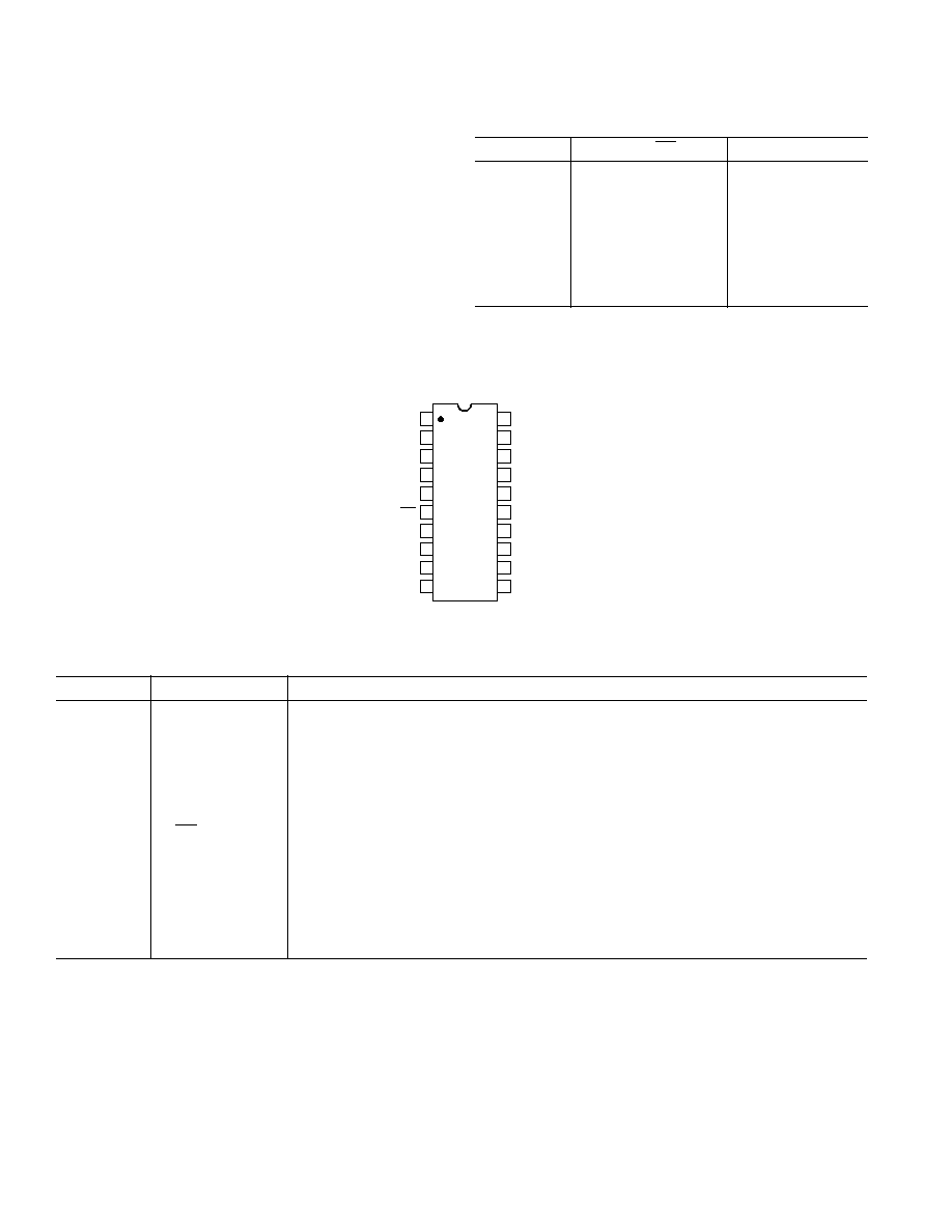
PIN CONFIGURATION
TOP VIEW
(Not to Scale)
20
19
18
17
16
15
14
13
12
11
1
2
3
4
5
6
7
8
9
10
AD9283
ENCODE
GND
V
D
VREF OUT
VREF IN
GND
A
IN
V
D
D7 (MSB)
D6
D5
D1
D2
D3
D4
V
DD
GND
PWRDWN
D0 (LSB)
A
IN
PIN FUNCTION DESCRIPTIONS
Pin Number
Name
Function
1
PWRDWN
Power-down function select; Logic HIGH for power-down mode (digital outputs go to
high impedance state).
2
VREF OUT
Internal Reference Output (+1.25 V typ); Bypass with 0.1
µ
F to Ground.
3
VREF IN
Reference Input for ADC (+1.25 V typ).
4, 9, 16
GND
Ground.
5, 8
V
D
Analog +3 V Power Supply.
6
A
IN
Analog Input for ADC (Can be left open if operating in single-ended mode, but recom-
mend connection to a 0.1
µ
F capacitor and a 25
resistor in series to ground for better
input matching).
7
A
IN
Analog Input for ADC
10
ENCODE
Encode Clock for ADC (ADC samples on rising edge of ENCODE).
1114, 1720
D7D4, D3D0
Digital Outputs of ADC.
15
V
DD
Digital output power supply. Nominally +2.5 V to +3.6 V.
Table I. Output Coding (VREF = +1.25 V)
Step
A
IN
A
IN
Digital Output
255
0.512
1111 1111
·
·
·
·
·
·
128
0.002
1000 0000
127
0.002
0111 1111
·
·
·
·
·
·
0
0.512
0000 0000
AD9283
5
REV. B
A
IN
V
DD
A
IN
33.3k
14.3k
33.3k
14.3k
Figure 2. Equivalent Analog Input Circuit
V
D
V
BIAS
REF IN
Figure 3. Equivalent Reference Input Circuit
ENCODE
V
D
Figure 4. Equivalent Encode Input Circuit
OUT
V
DD
Figure 5. Equivalent Digital Output Circuit
OUT
V
D
Figure 6. Equivalent Reference Output Circuit
A
IN
ENCODE
t
A
SAMPLE N
SAMPLE N+1
SAMPLE N+2
SAMPLE N+3
SAMPLE N+4
SAMPLE N+5
1/
fS
t
EL
t
EH
D7
D0
DATA N4
DATA N3
DATA N2
DATA N1
DATA N
DATA N+1
t
PD
t
V
Figure 1. Timing Diagram
AD9283
6
REV. B
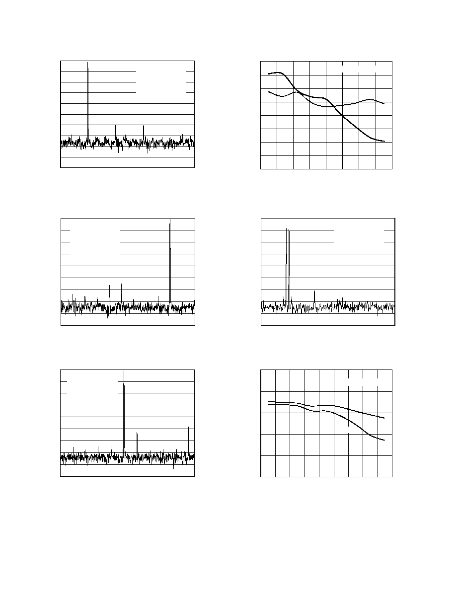
FREQUENCY
0
10
90
dB 50
60
70
80
30
40
20
100
ENCODE = 100 MSPS
A
IN
= 10.3MHz
SNR = 46.5dB
SINAD = 45dB
2nd = 57dBc
3rd = 54.5dBc
Figure 7. Spectrum: f
S
= 100 MSPS, f
IN
= 10.3 MHz
FREQUENCY
0
10
90
dB
50
60
70
80
30
40
20
ENCODE = 100 MSPS
A
IN
= 41MHz
SNR = 46.5dB
SINAD = 45dB
2nd = 58dBc
3rd = 52.5dBc
Figure 8. Spectrum: f
S
= 100 MSPS, f
IN
= 40 MHz
FREQUENCY
0
90
dB
ENCODE = 100 MSPS
A
IN
= 76MHz
SNR = 46dB
SINAD = 42.5dB
2nd = 46dBc
3rd = 53dBc
80
70
60
50
40
30
20
10
Figure 9. Spectrum: f
S
= 100 MSPS, f
IN
= 76 MHz
FREQUENCY A
IN
10
20
30
40
50
60
80
100
70
65
dB
45
40
30
55
50
60
2ND
3RD
35
ENCODE = 100 MSPS
Figure 10. Harmonic Distortion vs. A
IN
Frequency
FREQUENCY
0
10
90
dB
50
60
70
80
30
40
20
ENCODE = 100 MSPS
A
IN
1 = 9MHz
A
IN
2 = 10MHz
IMD = 52dBc
Figure 11. Two-Tone Intermodulation Distortion
FREQUENCY
10
20
30
40
50
60
80
90
55
dB
45
40
35
30
50
100
SNR
SINAD
ENCODE = 100 MSPS
Figure 12. SINAD/SNR vs. A
IN
Frequency
AD9283
7
REV. B
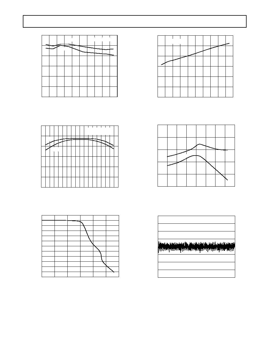
ENCODE RATE
10
100
49
48
dB
44
43
46
45
47
SINAD
A
IN
= 10.3MHz
SNR
20
30
40
50
60
70
80
90
Figure 13. SINAD/SNR vs. Encode Rate
ENCODE PULSEWIDTH HIGH ns
6.5
6
4.5
4
60
50
dB
10
0
30
20
40
ENCODE = 100 MSPS
A
IN
= 10.3MHz
SNR
SINAD
7
5.5
5
3.5
3
Figure 14. SINAD/SNR vs. Encode Pulsewidth High
BANDWIDTH MHz
0.5
1.0
5.5
0
600
dB
100
200
300
400
500
0.0
0.5
1.5
2.0
2.5
3.0
3.5
4.0
4.5
5.0
Figure 15. ADC Frequency Response: f
S
= 100 MSPS
ENCODE RATE
10
20
30
40
50
60
70
80
120
POWER mW
40
20
0
80
60
100
90
100
A
IN
= 10.3MHz
Figure 16. Analog Power Dissipation vs. Encode Rate
TEMPERATURE C
40
20
0
20
40
60
80
49
48
dB
44
46
45
47
60
100
SINAD
SNR
Figure 17. SINAD/SNR vs. Temperature
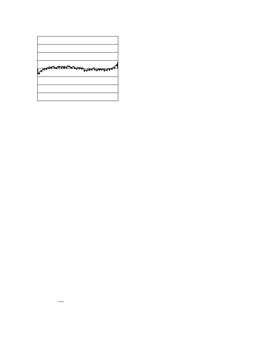
CODE
1.00
0.75
LSB
0.25
0.50
0.75
1.00
0.25
0.00
0.50
Figure 18. Differential Nonlinearity
AD9283
8
REV. B
CODE
2.0
LSB
0.5
1.0
1.5
2.0
0.5
0.0
1.0
1.5
Figure 19. Integral Nonlinearity
APPLICATIONS
Theory of Operation
The analog signal is applied differentially or single-endedly to
the inputs of the AD9283. The signal is buffered and fed for-
ward to an on-chip sample-and-hold circuit. The ADC core
architecture is a bit-per-stage pipeline type converter utilizing
switch capacitor techniques. The bit-per-stage blocks determine
the 5 MSBs and drive a FLASH converter to encode the 3 LSBs.
Each of the 5 MSB stages provides sufficient overlap and error
correction to allow optimization of performance with respect to
comparator accuracy. The output staging block aligns the data,
carries out the error correction and feeds the data to the eight
output buffers. The AD9283 includes an on-chip reference
(nominally 1.25 V) and generates all clocking signals from one
externally applied encode command. This makes the ADC easy
to interface with and requires very few external components for
operation.
ENCODE Input
The ENCODE input is fully TTL/CMOS compatible with a
nominal threshold of 1.5 V. Care was taken on the chip to
match clock line delays and maintain sharp clock logic transi-
tions. Any high speed A/D converter is extremely sensitive to
the quality of the sampling clock provided by the user. This
ADC uses an on-chip sample-and-hold circuit which is essen-
tially a mixer. Any timing jitter on the ENCODE will be com-
bined with the desired signal and degrade the high frequency
performance of the ADC. The user is advised to give commen-
surate thought to the clock source.
Analog Input
The analog input to the ADC is fully differential and both in-
puts are internally biased. This allows the most flexible use of ac
or dc and differential or single-ended input modes. For peak
performance the inputs are biased at 0.3
×
V
D
. See the specifi-
cation table for allowable common-mode range when dc cou-
pling the input. The inputs are also buffered to reduce the load
the user needs to drive. For best dynamic performance, the
impedances at A
IN
and A
IN
should be matched. The importance
of this increases with sampling rate and analog input frequency.
The nominal input range is 1.024 V p-p.
Digital Outputs
The digital outputs are TTL/CMOS compatible. The output
buffers are powered from a separate supply, allowing adjustment
of the output voltage swing to ease interfacing with 2.5 V or
3.3 V logic. The AD9283 goes into a low power state within two
clock cycles following the assertion of the PWRDWN input.
PWRDWN is asserted with a logic high. During power-down
the outputs transition to a high impedance state. The time it
takes to achieve optimal performance after disabling the power-
down mode is approximately 15 clock cycles. Care should be
taken when loading the digital outputs of any high speed ADC.
Large output loads create current transients on the chip that can
degrade the converter's performance.
Voltage Reference
A stable and accurate 1.25 V voltage reference is built into the
AD9283 (VREF OUT). In normal operation, the internal refer-
ence is used by strapping Pins 2 and 3 of the AD9283 together.
The input range can be adjusted by varying the reference volt-
age applied to the AD9283. No degradation in performance
occurs when the reference is adjusted
±
5%. The full-scale range
of the ADC tracks reference voltage changes linearly. Whether
used or not, the internal reference (Pin 2) should be bypassed
with a 0.1
µ
F capacitor to ground.
Timing
The AD9283 provides latched data outputs with four pipeline
delays. Data outputs are available one propagation delay (t
PD
)
after the rising edge of the encode command (Figure 1. Timing
Diagram). The minimum guaranteed conversion rate to the
ADC is 1 MSPS. The dynamic performance of the converter
will degrade at encode rates below this sample rate.
Evaluation Board
The AD9283 evaluation board offers an easy way to test the
AD9283. It only requires a 3 V supply, an analog input and
encode clock to test the AD9283. The board is shipped with the
100 MSPS grade ADC.
The analog input to the board accepts a 1 V p-p signal centered
at ground. J1 should be used (Jump E3E4, E18E19) to drive
the ADC through Transformer T1. J2 should be used for single-
ended input drive (Jump E19E21).
Both J1 and J2 are terminated to 50
on the PCB. Each analog
path is ac-coupled to an on-chip resistor divider which provides
the required dc bias.
A (TTL/CMOS Level) sample clock is applied to connector
J3 which is terminated through 50
on the PCB. This clock is
buffered by U5 which also provides the clocks for the 574
latches, DAC, and the off-card latch clock CLKCON. (Timing
can be modified at E17.)
There is a reconstruction DAC (AD9760) on the PCB. The
DAC is on the board to assist in debug only--the outputs
should not be used to measure performance of the ADC.
AD9283
9
REV. B
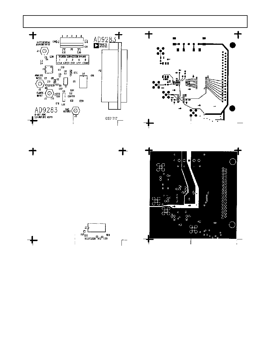
Figure 20. Printed Circuit Board Top Side Silkscreen
Figure 21. Printed Circuit Board Bottom Side Silkscreen
Figure 22. Printed Circuit Board Top Side Copper
Figure 23. Printed Circuit Board "Split" Power Layer
AD9283
10
REV. B
Figure 24. Printed Circuit Board Ground Layer
Figure 25. Printed Circuit Board Bottom Side Copper
EVALUATION BOARD BILL OF MATERIALS -- GS01717
#
QTY
REFDES
DEVICE
PACKAGE
VALUE
1
15
C1, C4C17
Ceramic Cap
0603
0.1
µ
F
2
4
C18C21
Tantalum Cap
BCAPTAJD
10
µ
F
3
24
E1E6, E8E10, E12E19,
E21, E34E39
W-HOLE
4
4
J1, J2, J3, J5
Connector
SMB
5
1
P1
5-Pin Connector
Wieland Connector
(P/N #25.602.2553.0 Top
P/N #Z5.530.0525.0 Bottom)
6
1
P2
37-Pin Connector
AMP-747462-2
7
5
R4, R9, R10, R21, R22
Resistor
1206
50
8
1
R7
Resistor
1206
25
9
1
R23
Resistor
1206
2K
10
1
T1
Transformer
Mini-Circuits T1-1T-KK81
11
1
U1
AD9283
SSOP-20
12
1
U3
AD9760
SOIC-28
13
1
U4
74ACQ574
SOIC-20
14
1
U5
SN74LVC86
SO14
AD9283
11
REV. B
14
10
11
12
13
1
2
3
4
5
6
7
8
9
10
11
12
13
14
15
16
17
18
19
20
21
22
23
24
25
26
27
28
29
30
31
32
33
34
35
36
37
VCC
Q0
Q1
Q2
Q3
Q4
Q5
Q6
Q7
CLOCK
OUT_EN
D0
D1
D2
D3
D4
D5
D6
D7
GND
P1
VA
VD
GND
VDL
VDAC
12345
VDL
C16
0.1
F
DA0
DA1
DA2
DA3
DA4
DA5
DA6
DA7
20
19
18
17
16
15
14
13
12
11
1
2
3
4
5
6
7
8
9
10
CLKLAT
U4
74ACQ574
D0
D1
D2
D3
GND
VDD
D4
D5
D6
D7
PWDN
REFOUT
REFIN
GND
VA
AIN
AIN
VA1
GND
U1
AD9283
C9
0.1
F
1
2
3
4
5
6
7
8
9
10
20
19
18
17
16
15
14
13
12
11
VD
PWDN
E8
E9
E10
VA
E1
E2
E5
E6
C5
0.1
F
C1
0.1
F
VA
C4
0.1
F
E3
E4
J1
R4
50
4
5
6
3
2
1
R7
25
C8
0.1
F
C7
0.1
F
R9
50
J2
E18
E19
E21
C17
0.1
F
E34
E35
E36
E37
E38
E39
E16
2
1
3
4
5
6
7
1B
1A
1Y
2A
2B
2Y
GND
4B
VCC
4A
4Y
3B
3A
3Y
13
14
12
11
10
9
8
E17
E15
VDL
U5
SN74LVC86
C13
0.1
F
CLKLAT
E12
E14
E13
CLKDAC
VDL
J3
R10
50
1
2
3
4
5
6
7
8
9
15
28
27
26
25
24
23
22
21
20
19
18
17
16
DB9
DB8
DB7
DB6
DB5
DB4
DB3
DB2
DB1
DB0
NC1
NC2
NC3
NC4
CLK
DVDD
DCOM
NC5
AVDD
COMP2
IOUTA
IOUTB
ACOM
COMP1
FSADJ
REFIO
REFLO
SLEEP
DA7
DA6
DA5
DA4
DA3
DA2
DA1
DA0
CLKDAC
C15
0.1
F
C10
0.1
F
VDAC
VDAC
J5
R21
50
R22
50
C14
0.1
F
VDAC
R23
2k
C12
0.1
F
C18
10
F
VA
C19
10
F
VD
C20
10
F
VDL
C21
10
F
VDAC
P2
C37DRPF
U3
AD9760
C11
0.1
F
VDL
T1
CLKCON
ENC
ENC
CLKCON
VA
C6
0.1
F
Figure 26. Printed Circuit Board Schematic
AD9283
12
REV. B
C3389b09/99
PRINTED IN U.S.A.
OUTLINE DIMENSIONS
Dimensions shown in inches and (mm).
20-Lead Shrink Small Outline Package (SSOP)
(RS-20)
20
11
10
1
0.295 (7.50)
0.271 (6.90)
0.311 (7.9)
0.301 (7.64)
0.212 (5.38)
0.205 (5.21)
PIN 1
SEATING
PLANE
0.008 (0.203)
0.002 (0.050)
0.07 (1.78)
0.066 (1.67)
0.0256
(0.65)
BSC
0.078 (1.98)
0.068 (1.73)
0.009 (0.229)
0.005 (0.127)
0.037 (0.94)
0.022 (0.559)
8°
0°