 | –≠–ª–µ–∫—Ç—Ä–æ–Ω–Ω—ã–π –∫–æ–º–ø–æ–Ω–µ–Ω—Ç: AD9433 | –°–∫–∞—á–∞—Ç—å:  PDF PDF  ZIP ZIP |
Document Outline
- Specifications
- Package drawings
- Ordering Guide
- Features
- Applications
- Product Description
- Absolute Maximum Ratings
- Functional Block Diagram
- Pin Function Description
- Circuit Description
- Typical Characteristics
- PRODUCT HIGHLIGHTS
- THERMAL CHARCTERISTICS
- EXPLANATION OF TEST LEVELS
- EQUIVALENT CIRCUITS
- TYPICAL IF SAMPLING PERFORMANCE
- APPLICATION NOTES
- USING THE AD9433
- EVALUATION BOARD LAYOUT
- DIAGRAMS
- AD9433 Timing Diagram
- Digital Output
- Analog Input
- Reference Output
- Encode Inputs
- Reference Input
- Using PECL to Drive the ENCODE Inputs
- Single-Ended Sine Source Encode Circuit
- Transformer-Coupled Encode Circuit
- Differential and Single-Ended Input Levels
- Transformer-Coupled Analog Input Circuit
- Driving the Analog Input with Two Transformers for Improved Even-Order Harmonics
- Evaluation Board Schematic 1
- Evaluation Board Schematic 2
- Evaluation Board Schematic 3
- Top Silkscreen
- Top Level Routing
- Ground Plane
- Power Plane
- Bottom Layer Routing
- Bottom Silkscreen
REV. 0
Information furnished by Analog Devices is believed to be accurate and
reliable. However, no responsibility is assumed by Analog Devices for its
use, nor for any infringements of patents or other rights of third parties that
may result from its use. No license is granted by implication or otherwise
under any patent or patent rights of Analog Devices.
a
AD9433
One Technology Way, P.O. Box 9106, Norwood, MA 02062-9106, U.S.A.
Tel: 781/329-4700
www.analog.com
Fax: 781/326-8703
© Analog Devices, Inc., 2001
12-Bit, 105 MSPS/125 MSPS
IF Sampling A/D Converter
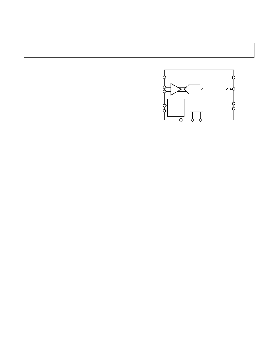
FUNCTIONAL BLOCK DIAGRAM
V
CC
AIN
AIN
ENCODE
ENCODE
REF
OUT
REF
IN
GND
V
DD
D11≠D0
DFS
SFDR
12
12
PIPELINE
ADC
T/H
ENCODE
TIMING
REF
OUTPUT
STAGING
AD9433
FEATURES
IF Sampling up to 350 MHz
SNR = 67.5 dB, f
IN
up to Nyquist @ 105 MSPS
SFDR = 83 dBc, f
IN
70 MHz @ 105 MSPS
SFDR = 72 dBc, f
IN
150 MHz @ 105 MSPS
2 V p-p Analog Input Range Option
On-Chip Clock Duty Cycle Stabilization
On-Chip Reference and Track/Hold
SFDR Optimization Circuit
Excellent Linearity:
DNL = 0.25 LSB (Typ)
INL = 0.5 LSB (Typ)
750 MHz Full Power Analog Bandwidth
Power Dissipation = 1.35 W Typical @ 125 MSPS
Two's Complement or Offset Binary Data Format
5.0 V Analog Supply Operation
2.5 V to 3.3 V TTL/CMOS Outputs
APPLICATIONS
Cellular Infrastructure Communication Systems
3G Single and Multicarrier Receivers
IF Sampling Schemes
Wideband Carrier Frequency Systems
Point to Point Radios
LMDS, Wireless Broadband
MMDS Base Station Units
Cable Reverse Path
Communications Test Equipment
Radar and Satellite Ground Systems
GENERAL INTRODUCTION
The AD9433 is a 12-bit monolithic sampling analog-to-digital
converter with an on-chip track-and-hold circuit and is designed
for ease of use. The product operates up to 125 MSPS conver-
sion rate and is optimized for outstanding dynamic performance
in wideband and high IF carrier systems.
The ADC requires a 5 V analog power supply and a differential
encode clock for full performance operation. No external refer-
ence or driver components are required for many applications.
The digital outputs are TTL/CMOS compatible and a separate
output power supply pin supports interfacing with 3.3 V or
2.5 V logic.
A user-selectable, on-chip proprietary circuit optimizes spurious-
free dynamic range (SFDR) versus signal-to-noise-and-distortion
(SINAD) ratio performance for different input signal frequencies,
providing as much as 83 dBc SFDR performance over the dc
to 70 MHz band.
The encode clock supports either differential or single-ended
input and is PECL-compatible. The output format is user-
selectable for binary or two's complement and provides an
overrange (OR) signal.
Fabricated on an advanced BiCMOS process, the AD9433 is
available in a thermally enhanced 52-lead plastic quad flatpack
specified over the industrial temperature range (≠40
∞C to
+85
∞C) and is pin-compatible with the AD9432.
PRODUCT HIGHLIGHTS
1. IF Sampling
The AD9433 maintains outstanding ac performance up to
input frequencies of 350 MHz. Suitable for 3G Wideband
Cellular IF sampling receivers.
2. Pin-Compatibility
This ADC has the same footprint and pin layout as the
AD9432, 12-Bit 80/105 MSPS ADC.
3. SFDR Performance
A user-selectable on-chip circuit optimizes SFDR performance
as much at 85 dBc from dc to 70 MHz.
4. Sampling Rate
At 125 MSPS, this ADC is ideally suited for current wireless
and wired broadband applications such as LMDS/MMDS
and cable reverse path.

REV. 0
≠2≠
AD9433≠SPECIFICATIONS
(V
DD
= 3.3 V, V
CC
= 5 V; internal reference; differential encode input, unless otherwise noted.)
Test
AD9433BSQ-105
AD9433BSQ-125
Parameter
Temp
Level
Min
Typ
Max
Min
Typ
Max
Unit
RESOLUTION
12
12
Bits
ACCURACY
No Missing Codes
Full
VI
Guaranteed
Guaranteed
Offset Error
Full
VI
≠5
0
+5
≠5
0
+5
mV
Gain Error
1
25 C
I
≠7
1
+3
≠7
1
+3
% FS
Differential Nonlinearity (DNL)
2
25 C
I
≠0.75
0.25
+0.75
≠0.75
0.3
+0.75
LSB
Full
VI
≠1
+1
≠1
+1
LSB
Integral Nonlinearity (INL)
2
25 C
I
≠1.0
0.5
+1.0
≠1.0
0.5
+1.0
LSB
Full
VI
≠1.3
+1.3
≠1.3
+1.3
LSB
THERMAL DRIFT
Offset Error
Full
V
≠50
≠50
ppm/ C
Gain Error
1
Full
V
≠125
≠125
ppm/ C
Reference
Full
V
±80
±80
ppm/ C
REFERENCE
Internal Reference Volatge (VREFOUT)
Full
I
2.4
2.5
2.6
2.4
2.5
2.6
V
Output Current (VREFOUT)
Full
V
100
100
µA
Input Current (VREFIN)
Full
IV
50
50
µA
ANALOG INPUTS
Differential Input Voltage Range
Full
V
2.0
2.0
V
(
AIN, AIN)
Common-Mode Voltage
Full
V
4.0
4.0
V
Input Resistance
Full
VI
2
3
4
2
3
4
k
Input Capacitance
Full
V
4
4
pF
Analog Bandwidth, Full Power
Full
V
750
750
MHz
POWER SUPPLY
V
CC
Full
IV
4.75
5.0
5.25
4.75
5.0
5.25
V
V
DD
Full
IV
2.7
3.3
2.7
3.3
V
Power Dissipation
3
Full
VI
1275
1425
1350
1500
mW
Power Supply Rejection Ratio (PSRR)
25 C
I
3
3
mV/V
IV
CC
2
Full
VI
255
285
270
300
mA
IV
DD
2
Full
VI
12.5
14
16
18
mA
ENCODE INPUTS
Internal Common-Mode Bias
Full
V
3.75
3.75
V
Differential Input (ENC ≠
ENC)
Full
V
500
500
mV
Input Voltage Range
Full
IV
≠0.5
V
CC
+ 0.05
≠0.5
V
CC
+ 0.05 V
Input Common-Mode Range
Full
IV
2.0
4.25
2.0
4.25
V
Input Resistance
Full
VI
6
6
k
Input Capacitance
25 C
V
3
3
pF
DIGITAL INPUTS
Input High Voltage
Full
I
2.0
2.0
V
Input Low Voltage
Full
I
0.8
0.8
V
Input High Current (VIN = 5 V)
Full
V
50
50
µA
Input Low Current (VIN = 0 V)
Full
V
50
50
µA
DIGITAL OUTPUTS
Logic "1" Voltage
Full
VI
V
DD
≠ 0.05
V
DD
≠ 0.05
V
Logic "0" Voltage
Full
VI
0.05
0.05
V
Output Coding
Two's Complement or Offset Binary
NOTES
1
Gain error and gain temperature coefficients are based on the ADC only (with a fixed 2.5 V external reference and a 2 V p-p differential analog input).
2
SFDR disabled (SFDR = GND) for DNL and INL specifications.
3
Power dissipation measured with rated encode and a dc analog input (Outputs Static, I
VDD
= 0). I
VCC
and I
VDD
measured with 10.3 MHz analog input @ ≠0.5 dBFS.
Specifications subject to change without notice.
DC SPECIFICATIONS
REV. 0
≠3≠
AD9433
Test
AD9433BSQ-105
AD9433BSQ-125
Parameter
Temp
Level
Min
Typ
Max
Min
Typ
Max
Unit
DYNAMIC PERFORMANCE
*
Signal-to-Noise Ratio (SNR)
(Without Harmonics)
f
IN
= 10.3 MHz
25 C
I
66.5
68.0
66.0
67.7
dB
f
IN
= 49 MHz
25 C
I
65.5
67.5
64.0
66.0
dB
f
IN
= 70 MHz
25 C
V
67.0
65.4
dB
f
IN
= 150 MHz
25 C
V
65.4
62.0
dB
f
IN
= 250 MHz
25 C
V
63.7
60.0
dB
Signal-to-Noise Ratio and Distortion (SINAD)
(With Harmonics)
f
IN
= 10.3 MHz
25 C
I
66.0
68.0
65.0
67.0
dB
f
IN
= 49 MHz
25 C
I
64.0
67.5
63.5
65.5
dB
f
IN
= 70 MHz
25 C
V
66.9
64.5
dB
f
IN
= 150 MHz
25 C
V
64.0
61.5
dB
f
IN
= 250 MHz
25 C
V
61.2
57.7
dB
Effective Number of Bits
f
IN
= 10.3 MHz
25 C
I
11.1
10.9
Bits
f
IN
= 49 MHz
25 C
I
11.0
10.7
Bits
f
IN
= 70 MHz
25 C
V
10.9
10.6
Bits
f
IN
= 150 MHz
25 C
V
10.4
10.0
Bits
f
IN
= 250 MHz
25 C
V
9.9
9.4
Bits
2nd and 3rd Harmonic Distortion
f
IN
= 10.3 MHz
25 C
I
≠78
≠85
≠76
≠85
dBc
f
IN
= 49 MHz
25 C
I
≠73
≠80
≠72
≠76
dBc
f
IN
= 70 MHz
25 C
V
≠83
≠78
dBc
f
IN
= 150 MHz
25 C
V
≠72
≠67
dBc
f
IN
= 250 MHz
25 C
V
≠67
≠65
dBc
Worst Other Harmonic or Spur
(Excluding Second and Third)
f
IN
= 10.3 MHz
25 C
I
≠88
≠92
≠84
≠90
dBc
f
IN
= 49 MHz
25 C
I
≠82
≠89
≠82
≠87
dBc
f
IN
= 70 MHz
25 C
V
≠87
≠85
dBc
f
IN
= 150 MHz
25 C
V
≠87
≠84
dBc
f
IN
= 250 MHz
25 C
V
≠85
≠76
dBc
Two-Tone Intermod Distortion (IMD3)
f
IN1
= 49.3 MHz, f
IN2
= 50.3 MHz
25 C
V
≠92
≠90
dBc
f
IN1
= 150 MHz, f
IN2
= 151 MHz
25 C
V
≠80
≠76
dBc
*SNR/Harmonics based on an analog input voltage of ≠0.5 dBFS referenced to a 2 V full-scale input range. Harmonics are specified with the SFDR active
(SFDR = +5 V). SNR/SINAD specified with SFDR disabled (SFDR = Ground).
Specifications subject to change without notice.
AC SPECIFICATIONS
(V
DD
= 3.3 V, V
CC
= 5 V; differential encode input, unless otherwise noted.)
SWITCHING SPECIFICATIONS
Test
AD9433BSQ-105
AD9433BSQ-125
Parameter
Temp
Level
Min
Typ
Max
Min
Typ
Max
Unit
Encode Rate
Full
IV
10
105
10
125
MSPS
Encode Pulsewidth High (t
EH
)
Full
IV
2.9
2.4
ns
Encode Pulsewidth Low (t
EL
)
Full
IV
2.9
2.4
ns
Aperture Delay (t
A
)
25 C
V
2.1
2.1
ns
Aperture Uncertainty (Jitter)
1
25 C
V
0.25
0.25
ps rms
Output Valid Time (t
V
)
2
Full
VI
2.5
4.0
2.5
4.0
ns
Output Propagation Delay (t
PD
)
2
Full
VI
4.0
5.5
4.0
5.5
ns
Output Rise Time (t
R
)
Full
V
2.1
2.1
ns
Output Fall Time (t
F
)
Full
V
1.9
1.9
ns
Out of Range Recovery Time
25 C
V
2
2
ns
Transient Response Time
25 C
V
2
2
ns
Latency
Full
IV
10
10
Cycles
NOTES
1
Aperture uncertainty includes contribution of the AD9433, crystal clock reference, and encode drive circuit.
2
t
V
and t
PD
are measured from the transition points of the ENCODE input to the 50%/50% levels of the digital output swing. The digital output load during testing is
not to exceed an ac load of 10 pF or a dc current of 50
µA. Rise and fall times measured from 10% to 90%.
Specifications subject to change without notice.
(V
DD
= 3.3 V, V
CC
= 5 V; differential encode input, unless otherwise noted.)
REV. 0
AD9433
≠4≠
EXPLANATION OF TEST LEVELS
Test Level
I
100% production tested.
II
100% production tested at 25 C and guaranteed by design
and characterization at specified temperatures.
III Sample Tested Only
IV Parameter is guaranteed by design and characterization testing.
V
Parameter is a typical value only.
VI 100% production tested at 25 C and guaranteed by design
and characterization for industrial temperature range.
THERMAL CHARCTERISTICS
Thermal Resitance
52-Lead PowerQuad
Æ
4 LQFP_ED
JA
= 25
∞C/W, Soldered Heat Sink, No Airflow
JA
= 33
∞C/W, Unsoldered Heat Sink, No Airflow
JC
= 2
∞C/W, Bottom of Package (Heat Sink)
Simulated typical performance for 4-layer JEDEC board, horizontal orientation.
ABSOLUTE MAXIMUM RATINGS
*
Parameter
Min
Max
Unit
ELECTRICAL
V
DD
Voltage
≠0.5
+6.0
V
V
CC
Voltage
≠0.5
+6.0
V
Analog Input Voltage
≠0.5
V
CC
+ 0.5
V
Digital Input Voltage
≠0.5
V
CC
+ 0.5
V
Digital Output Current
20
mA
ENVIRONMENTAL
Operating Temperature
Range (Ambient)
≠40
+85
C
Maximum Junction
Temperature
+150
C
Storage Temperature
Range (Ambient)
≠65
+125
C
*Stresses greater than those listed under Absolute Maximum Ratings may cause
permanent damage to the device. This is a stress rating only; functional operation
of the device at these or any other conditions above those indicated in the
operational section of this specification is not implied. Exposure to absolute
maximum rating conditions for extended periods may affect device reliability.
ORDERING GUIDE
Model
Temperature Range
Package Description
Package Option
AD9433BSQ-105
≠40
∞C to +85∞C (Ambient)
52-Lead Plastic Thermally Enhanced Quad Flatpack
SQ-52
AD9433BSQ-125
≠40
∞C to +85∞C (Ambient)
52-Lead Plastic Thermally Enhanced Quad Flatpack
SQ-52
AD9433/PCB
25
∞C
Evaluation Board with AD9433BSQ-125
(Supports ≠ 105 Evaluation)
CAUTION
ESD (electrostatic discharge) sensitive device. Electrostatic charges as high as 4000 V readily
accumulate on the human body and test equipment and can discharge without detection. Although
the AD9433 features proprietary ESD protection circuitry, permanent damage may occur on
devices subjected to high-energy electrostatic discharges. Therefore, proper ESD precautions are
recommended to avoid performance degradation or loss of functionality.
WARNING!
ESD SENSITIVE DEVICE
PowerQuad is a registered trademark of AMkor Technology, Inc.

REV. 0
AD9433
≠5≠
PIN FUNCTION DESCRIPTIONS
Pin Number
Mnemonic
Function
1, 3, 4, 9, 11, 33, 34, 35, 38, 39, 40,
GND
Analog Ground
43, 48, 51
2, 5, 6, 10, 36, 37, 44, 47, 52
V
CC
Analog Supply (5 V)
7
ENCODE
Encode Clock for ADC-Complementary
8
ENCODE
Encode Clock for ADC-True (ADC samples on rising edge of
ENCODE)
14
OR
Out of Range Output
15≠20, 25≠30
D11≠D0
Digital Output
13, 22, 23, 32
V
DD
Digital Output Power Supply (3 V)
12, 21, 24, 31
DGND
Digital Output Ground
41
DFS
Data Format Select. Low = Two's Complement, High = Binary;
Floats Low
42
SFDR MODE
CMOS control pin that enables (SFDR MODE = 1), a proprietary
circuit that may improve the spurious free dynamic range (SFDR)
performance of the AD9433. It is useful in applications where the
dynamic range of the system is limited by discrete spurious
frequency content caused by nonlinearities in the ADC transfer
function. SFDR MODE = 0 for normal operation; Floats Low.
45
VREFIN
Reference Input for ADC (2.5 V typical)
46
VREFOUT
Internal Reference Output (2.5 V typical); bypass with 0.1
µF to
Ground
49
AIN
Analog Input-True
50
AIN
Analog Input-Complement
PIN CONFIGURATION
52 51 50 49 48
43 42 41 40
47 46 45 44
14 15 16 17 18 19 20 21 22 23 24 25 26
1
2
3
4
5
6
7
8
9
10
11
13
12
PIN 1
IDENTIFIER
TOP VIEW
(Not to Scale)
39
38
37
36
35
34
33
32
31
30
29
28
27
AD9433BSQ
OR
(
MSB) D11
D10
D9
D8
D7
D6
DGND
V
DD
V
DD
DGND
D5
D4
V
CC
GND
AIN
AIN
GND
V
CC
VREFOUT
VREFIN
V
CC
GND
SFDR MODE
DFS
GND
GND
V
CC
GND
GND
V
CC
V
CC
ENCODE
ENCODE
GND
V
CC
GND
DGND
V
DD
GND
GND
V
CC
V
CC
GND
GND
GND
V
DD
DGND
D0 (LSB)
D1
D2
D3

REV. 0
AD9433
≠6≠
DEFINITIONS OF SPECIFICATIONS
Analog Bandwidth
The analog input frequency at which the spectral power of the
fundamental frequency (as determined by the FFT analysis) is
reduced by 3 dB.
Aperture Delay
The delay between the 50% point of the rising edge of the
ENCODE command and the instant at which the analog
input is sampled.
Aperture Uncertainty (Jitter)
The sample-to-sample variation in aperture delay.
Differential Analog Input Resistance, Differential Analog
Input Capacitance, and Differential Analog Input Impedance
The real and complex impedances measured at each analog
input port. The resistance is measured statically and the capaci-
tance and differential input impedances are measured with a
network analyzer.
Differential Analog Input Voltage Range
The peak-to-peak differential voltage that must be applied to
the converter to generate a fullscale response. Peak differen-
tial voltage is computed by observing the voltage on a single
pin and subtracting the voltage from the other pin, which is
180 degrees out of phase. Peak to peak differential is computed
by rotating the inputs phase 180 degrees and taking the peak
measurement again. Then the difference is computed between
both peak measurements.
Differential Nonlinearity
The deviation of any code width from an ideal 1 LSB step.
Effective Number of Bits
The effective number of bits (ENOB) is calculated from the
measured SNR based on the equation:
ENOB
SNR
dB
Amplitude
Input Amplitude
MEASURED
=
≠ .
+
Full - Scale
.
1 76
20
6 02
log
Encode Pulsewidth/Duty Cycle
Pulsewidth high is the minimum amount of time that the
ENCODE pulse should be left in logic "1" state to achieve
rated performance; pulsewidth low is the minimum time
ENCODE pulse should be left in low state. See timing impli-
cations of changing t
ENCH
in text. At a given clock rate, these
specs define an acceptable Encode duty cycle.
Full-Scale Input Power
Expressed in dBm. Computed using the following equation:
Power
V
Z
Full Scale
FullScale
rms
=
10
0 001
2
log
.
Gain
Gain error is the difference between the measured and ideal
full-scale input voltage range of the ADC.
Harmonic Distortion
The ratio of the rms signal amplitude fundamental frequency to
the rms signal amplitude of a single harmonic component (second,
third, etc.), reported in dBc.
Integral Nonlinearity
The deviation of the transfer function from a reference line
measured in fractions of 1 LSB using a best fit straight line
determined by a least square curve fit.
Minimum Conversion Rate
The encode rate at which the SNR of the lowest analog signal
frequency drops by no more than 3 dB below the guaranteed limit.
Maximum Conversion Rate
The maximum encode rate at which parametric testing is performed.
Output Propagation Delay
The delay between a differential crossing of ENCODE and
ENCODE and the time when all output data bits are within
valid logic levels.
Noise (for Any Range within the ADC)
V
=
Z
0.001
10
FS
≠ SNR
≠ Signal
10
NOISE
dBm
dBc
dBFS
◊
◊
Where Z is the input impedance, FS is the full scale of the device
for the frequency in question, SNR is the value for the particular
input level, and SIGNAL is the signal level within the ADC
reported in dB below full scale. This value includes both thermal
and quantization noise.
Power Supply Rejection Ratio
The ratio of a change in input offset voltage to a change in
power supply voltage.
Signal-to-Noise and Distortion (SINAD)
The ratio of the rms signal amplitude (set 1 dB below full scale)
to the rms value of the sum of all other spectral components,
including harmonics but excluding dc.
Signal-to-Noise Ratio (without Harmonics)
The ratio of the rms signal amplitude (set at 1 dB below full
scale) to the rms value of the sum of all other spectral compo-
nents, excluding the first five harmonics and dc.
Spurious-Free Dynamic Range (SFDR)
The ratio of the rms signal amplitude to the rms value of the peak
spurious spectral component. The peak spurious component
may or may not be a harmonic. May be reported in dBc (i.e.,
degrades as signal level is lowered), or dBFS (always related back
to converter full scale).
Two-Tone Intermodulation Distortion Rejection
The ratio of the rms value of either input tone (f
1
, f
2
) to the rms
value of the worst third order intermodulation product; reported
in dBc. Products are located at 2f
1
≠ f
2
and 2f
2
≠ f
1
.
Two-Tone SFDR
The ratio of the rms value of either input tone (f
1
, f
2
) to the rms
value of the peak spurious component. The peak spurious com-
ponent may or may not be an IMD product. May be reported in
dBc (i.e., degrades as signal level is lowered), or in dBFS (always
related back to converter full scale).
Worst Other Spur
The ratio of the rms signal amplitude to the rms value of the
worst spurious component (excluding the second and third
harmonic) reported in dBc.

REV. 0
≠7≠
AD9433
SAMPLE N≠1
SAMPLE N
SAMPLE N+1
SAMPLE N+8
SAMPLE N+9
SAMPLE N+10
A
IN
ENCODE
ENCODE
D11≠D0
t
A
t
EH
t
EL
t
PD
t
V
1/f
S
DATA N≠11
DATA N≠10
DATA
N≠9
DATA
N≠2
DATA N≠1
DATA N
DATA N+1
Figure 1. AD9433 Timing Diagram
EQUIVALENT CIRCUITS
VREFOUT
V
CC
Figure 4. Reference Output
V
CC
AIN
AIN
15k
15k
3.75k
3.75k
Figure 3. Analog Input
V
CC
VREFIN
Figure 6. Reference Input
24k
24k
8k
8k
V
CC
ENCODE
ENCODE
Figure 5. Encode Inputs
V
DD
D
X
Figure 2. Digital Output

REV. 0
AD9433
≠8≠
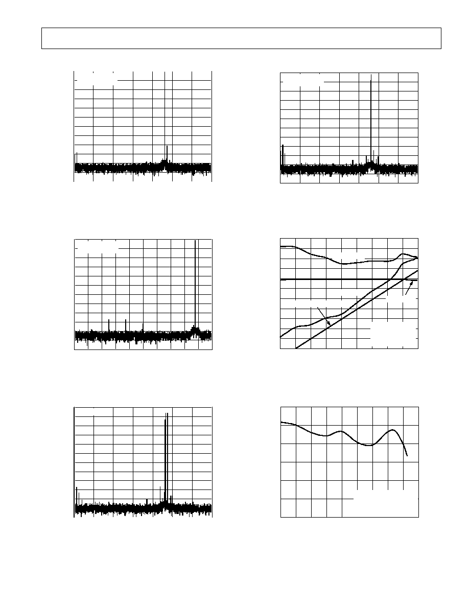
≠Typical Performance Characteristics
FREQUENCY ≠ MHz
≠120
0
dB
13.1
SNR = 67.5dB
SFDR = 85.0dBFS
26.3
39.4
52.5
≠110
≠100
≠90
≠80
≠70
≠60
≠50
≠40
≠30
≠20
≠10
0
TPC 1. FFT: f
S
= 105 MSPS, f
IN
= 49.3 MHz, Differential
AIN @ ≠0.5 dBFS, SFDR Enabled
FREQUENCY ≠ MHz
≠120
0
dB
13.1
SNR = 68.0dB
SFDR = 80.0dBFS
26.3
39.4
52.5
≠110
≠100
≠90
≠80
≠70
≠60
≠50
≠40
≠30
≠20
≠10
0
TPC 2. FFT: f
S
= 105 MSPS, f
IN
= 49.3 MHz, Differential
AIN @ ≠0.5 dBFS, SFDR Disabled
FREQUENCY ≠ MHz
≠120
0
dB
SNR = 67.7dB
SFDR = 76.0dBFS
62.5
≠110
≠100
≠90
≠80
≠70
≠60
≠50
≠40
≠30
≠20
≠10
0
46.8
31.2
15.6
TPC 3. FFT: f
S
= 125 MSPS, f
IN
= 49.3 MHz, Differential
AIN @ ≠0.5 dBFS, SFDR Enabled
AIN ≠ MHz
≠60
0
50
dBc
100
150
200
250
≠65
≠70
≠75
≠80
≠85
≠90
≠95
2ND HARMONIC
3RD HARMONIC
WORST OTHER
TPC 4. Harmonics (Second, Third, Worst Other) vs. AIN
Frequency. AIN @ ≠0.5 dBFS, f
S
= 105 MSPS, SFDR Enabled
AIN
≠ Hz
60
0
50
SNR/SINAD
≠
dB
100
150
200
250
61
62
63
64
65
66
67
SINAD
SNR
68
300
11.1
10.9
10.8
10.6
10.4
10.3
10.1
9.9
9.8
ENOBs
≠
Bits
TPC 5. SNR vs. AIN Frequency. Differential AIN @
≠0.5 dBFS, 105 MSPS, SFDR Disabled
ENCODE ≠ MSPS
60
10
30
SNR/SINAD
≠
dB
50
70
90
110
65
70
75
80
85
90
95
SINAD
SNR
100
140
3RD
≠dBc
2ND
≠dBc
TPC 6. SNR/SINAD and Harmonic Distortion vs.
Encode Frequency. Differential AIN @ ≠0.5 dBFS
REV. 0
AD9433
≠9≠
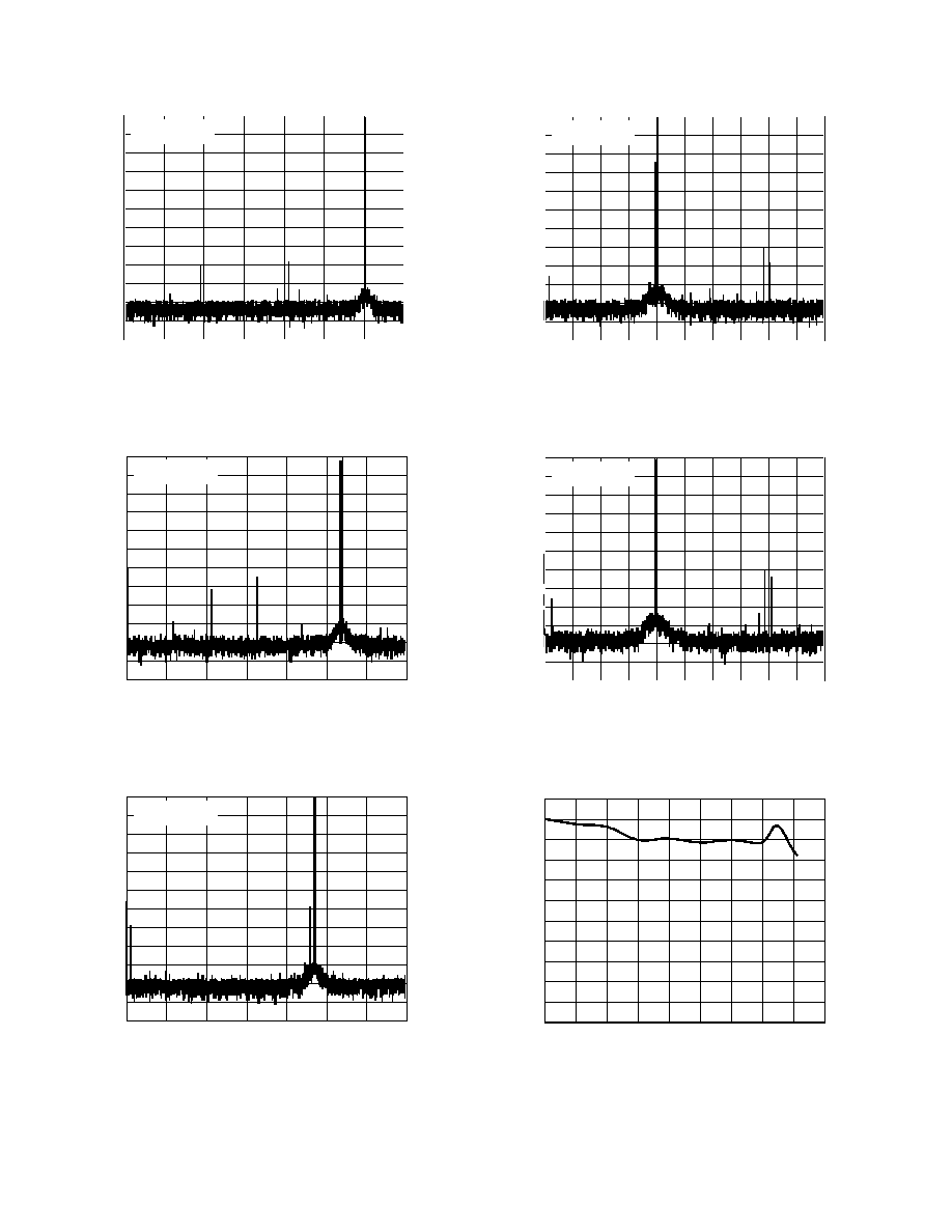
FREQUENCY ≠ MHz
≠120
0
dB
22.5
30.0
45.0
52.5
≠110
≠100
≠90
≠80
≠70
≠60
≠50
≠40
≠30
≠20
≠10
0
37.5
15.0
7.5
IMD3 = 92dBFS
TPC 7. FFT: f
S
= 105 MSPS, f
IN
= 49.3 MHz and 50.3 MHz,
Differential AIN @ ≠7 dBFS for Each Tone, SFDR Enabled
AIN LEVEL ≠ dBFS
0
≠90
SFDR
≠
dB
10
110
f
S
= 105MSPS
f
IN
= 49.3MHz
DIFFERENTIAL AIN
SFDR ENABLED
90dBFS
REFERENCE
SFDR dBFS
SFDR dBc
SNR dBFS
≠80
≠70
≠60
≠50
≠40
≠30
≠20
≠10
0
20
30
40
50
60
70
80
90
100
TPC 8. SNR and SFDR vs. AIN
Level, f
S
= 105 MSPS,
f
IN
= 49.3 MHz, Differential AIN, SFDR Enabled
AIN LEVEL ≠ dBFS
≠90
THIRD ORDER IMD
≠
dB
110
≠80
≠70
≠60
≠50
≠40
≠30
≠20
≠10
0
50
60
70
80
90
100
TPC 9. Third Order IMD vs. AIN Level, f
S
= 105 MSPS,
f
IN
= 49.3 MHz and 50.3 MHz, Differential AIN, SFDR
Enabled
AIN ≠ MHz
55
SNR/SINAD
≠
dB
SNR
10.3
SINAD
49.3
80.3
170.3
250.3
57
59
61
63
65
67
69
8.9
ENOB
≠
Bits
9.3
9.6
9.9
10.3
10.6
10.9
11.3
TPC 10. SNR and SINAD vs. AIN
Frequency.
Differential AIN @ ≠0.50 dBFS, f
S
= 125 MSPS,
SFDR Enabled
AIN COMMON-MODE VOLTAGE ≠ V
0
3.5
dB
10
20
30
40
50
60
70
2ND HARMONIC
3RD HARMONIC
SNR
3.6
3.7
3.8
3.9
4.0
4.1
4.2
4.3
4.4
4.5
80
90
100
TPC 11. Dynamic Performance vs. AIN
Common-Mode
Voltage. Differential AIN @ ≠0.5 dBFS, f
IN
= 49.3 MHz,
f
S
= 105 MSPS
AIN ≠ MHz
60
SNR
≠
dB
10.3
49.3
80.3
170.3
250.3
61
62
63
64
65
66
69
68
67
≠40 C
+25 C
+85 C
TPC 12. SNR vs. AIN Frequency/Temperature,
f
S
= 105 MSPS, Differential AIN, SFDR Disabled

REV. 0
AD9433
≠10≠
DUTY CYCLE HIGH ≠ %
≠60
0
20
DYNAMIC PERFORMANCE
≠
dB
≠65
≠70
≠75
≠80
≠85
≠90
≠95
2ND HARMONIC (dBc)
3RD HARMONIC (dBc)
WORST OTHER (dBc)
SNR (dB)
30
40
50
60
70
80
90
10
TPC 13. Dynamic Performance vs. Encode Duty Cycle
f
S
= 105 MSPS, f
IN
= 49.3 MHz, Differential AIN @ ≠0.5 dBFS,
SFDR Enabled
≠0.75
0
512
1024
1536
2048
2560
3072
3584
4095
0
0.25
≠0.50
≠0.25
0.50
0.75
OUTPUT CODE
INL
≠
LSBs
TPC 14. Integral Nonlinearity vs. Output Code
with SFDR Disabled
≠0.5
0
512
1024
1536
2048
2560
3072
3584
4095
≠0.4
≠0.3
≠0.2
≠0.1
0
0.1
0.2
0.3
0.4
0.5
OUTPUT CODE
DNL
≠
LSBs
TPC 15. Differential Nonlinearity vs. Output Code
ENCODE FREQUENCY ≠ MHz
180
I
CC
≠
mA
0
I
CC
(mA)
25
50
75
100
125
200
220
240
260
280
300
I
DD
(mA)
0
I
DD
≠
mA
3
6
9
12
15
18
TPC 16. I
DD
and I
CC
vs. Encode Rate. f
IN
= 10.3 MHz,
Differential AIN @ ≠0.5 dBFS
≠0.75
0
512
1024
1536
2048
2560
3072
3584
4095
0
0.25
≠0.50
≠0.25
0.50
0.75
OUTPUT CODE
INL
≠
LSBs
TPC 17. Integral Nonlinearity vs. Output Code with
SFDR Enabled
FREQUENCY ≠ MHz
≠120
0
dB
7.68
15.36
23.04
30.72
≠110
≠100
≠90
≠80
≠70
≠60
≠50
≠40
≠30
≠20
≠10
0
TPC 18. FFT: f
S
= 61.44 MSPS, f
IN
= 46.08 MHz, 4 WCDMA
Carriers, Differential AIN, SFDR Enabled
REV. 0
AD9433
≠11≠
TYPICAL IF SAMPLING PERFORMANCE
FREQUENCY ≠ MHz
≠120
0
7.5
dB
15.0
SNR = 66.8dB
SFDR = 83.0dBFS
22.5
30.0
37.5
45.0
52.5
≠110
≠100
≠90
≠80
≠70
≠60
≠50
≠40
≠30
≠20
≠10
0
TPC 19. FFT: f
S
= 105 MSPS, f
IN
= 70.3 MHz, Differential
AIN @ ≠0.5 dBFS, SFDR Enabled
FREQUENCY ≠ MHz
≠120
0
6.2
dB
12.5
SNR = 65.5dB
SFDR = 78.0dBFS
≠110
≠100
≠90
≠80
≠70
≠60
≠50
≠40
≠30
≠20
≠10
0
18.7
25.0
31.2
37.5
43.7
50.0
56.2
62.5
TPC 20. FFT: f
S
= 125 MSPS, f
IN
= 70.3 MHz, Differential
AIN @ ≠0.5 dBFS, SFDR Enabled
FREQUENCY ≠ MHz
≠120
0
7.5
dB
15.0
IMD3 ≠ 85dBc
≠110
≠100
≠90
≠80
≠70
≠60
≠50
≠40
≠30
≠20
≠10
0
22.5
30.0
37.5
45.0
52.5
TPC 21. FFT: f
S
= 105 MSPS, f
IN
= 69.3 and 70.3 MHz,
Differential AIN @ ≠7 dBFS for Each Tone, SFDR Enabled
FREQUENCY ≠ MHz
≠120
0
7.5
dB
15.0
SNR = 67.0dB
SFDR = 80.0dBFS
≠110
≠100
≠90
≠80
≠70
≠60
≠50
≠40
≠30
≠20
≠10
0
22.5
30.0
37.5
45.0
52.5
TPC 22. FFT: f
S
= 105 MSPS, f
IN
= 70.3 MHz, Differential
AIN @ ≠0.5 dBFS, SFDR Disabled
AIN LEVEL ≠ dBFS
0
≠90
SNR/SFDR
≠
dB
10
20
30
40
50
60
70
80dBFS REFERENCE LINE
SNR ≠ dBFS
f
S
= 105MSPS
f
IN
= 70.3MHz
DIFFERENTIAL AIN
SFDR ENABLED
SFDR ≠ dBc
SFDR ≠ dBFS
80
90
100
110
≠80
≠70
≠60
≠50
≠40
≠30
≠20
≠10
0
TPC 23. SNR/SFDR vs. AIN Level
dBFS
≠90
dBFS
f
S
= 105MSPS
f
IN
= 70.3MHz AND 69.3MHz
DIFFERENTIAL AIN
SFDR ENABLED
≠110
≠80
≠70
≠60
≠50
≠40
≠30
≠20
≠10
0
≠100
≠90
≠80
≠70
≠60
≠50
TPC 24. Third Order IMD vs. AIN Level,
f
S
= 105 MSPS, f
IN
= 70.3 MHz and 69.3 MHz,
Differential AIN, SFDR Enabled
REV. 0
AD9433
≠12≠
FREQUENCY ≠ MHz
≠120
0
7.5
dB
15.0
SNR = 64.0dB
SFDR = 78.0dBFS
≠110
≠100
≠90
≠80
≠70
≠60
≠50
≠40
≠30
≠20
≠10
0
22.5
30.0
37.5
45.0
52.5
TPC 25. FFT: f
S
= 105 MSPS, f
IN
= 150.3 MHz, Differential
AIN @ ≠0.5 dBFS, SFDR Enabled
FREQUENCY ≠ MHz
≠120
0
7.5
dB
15.0
SNR = 61.2dB
SFDR = 67.0dBFS
≠110
≠100
≠90
≠80
≠70
≠60
≠50
≠40
≠30
≠20
≠10
0
22.5
30.0
37.5
45.0
52.5
TPC 26. FFT: f
S
= 105 MSPS, f
IN
= 250.3 MHz, Differential
AIN @ ≠0.5 dBFS, SFDR Enabled
FREQUENCY ≠ MHz
≠120
0
7.5
dB
15.0
SNR = 55.3dB
SFDR = 61.0dBFS
≠110
≠100
≠90
≠80
≠70
≠60
≠50
≠40
≠30
≠20
≠10
0
22.5
30.0
37.5
45.0
52.5
TPC 27. FFT: f
S
= 105 MSPS, f
IN
= 350.3 MHz, Differential
AIN @ ≠0.5 dBFS, SFDR Enabled
FREQUENCY ≠ MHz
≠120
0
6.25
dB
12.5
SNR = 62.0dB
SFDR = 70.0dBFS
≠110
≠100
≠90
≠80
≠70
≠60
≠50
≠40
≠30
≠20
≠10
0
18.7
25.0
31.2
37.5
43.7
50.0
56.2
62.5
TPC 28. FFT: f
S
= 125 MSPS, f
IN
= 150.3 MHz, Differential
AIN @ ≠0.5 dBFS, SFDR Enabled
FREQUENCY ≠ MHz
≠120
0
6.2
dB
SNR = 54.6dB
SFDR = 58.0dBFS
≠110
≠100
≠90
≠80
≠70
≠60
≠50
≠40
≠30
≠20
≠10
0
18.7
25.0
31.2
37.5
43.7
50.0
56.2
62.5
12.5
TPC 29. FFT: f
S
= 125 MSPS, f
IN
= 350.3 MHz, Differential
AIN @ ≠0.5 dBFS, SFDR Enabled
dBFS
≠60
≠90
dBFS
≠70
≠80
≠90
≠100
≠110
≠50
≠40
≠30
≠20
≠10
0
≠80
≠70
≠60
≠50
≠40
≠30
≠20
≠10
0
IMD3
TPC 30. Third Order IMD vs. AIN Level, f
S
= 105 MSPS,
f
IN
= 150.3 and 151.3 MHz, Differential AIN, SFDR Enabled

REV. 0
AD9433
≠13≠
APPLICATION NOTES
Theory of Operation
The AD9433 is a multibit pipeline converter that uses a switched
capacitor architecture. Optimized for high speed, this converter
provides flat dynamic performance up to and beyond the Nyquist
limit. DNL transitional errors are calibrated at final test to a
typical accuracy of 0.25 LSB or less.
USING THE AD9433
ENCODE Input
Any high-speed A/D converter is extremely sensitive to the quality
of the sampling clock provided by the user. A track/hold circuit
is essentially a mixer, and any noise, distortion, or timing jitter
on the clock will be combined with the desired signal at the A/D
output. For that reason, considerable care has been taken in the
design of the ENCODE input of the AD9433, and the user is
advised to give commensurate thought to the clock source.
The AD9433 has an internal clock duty cycle stabilization
circuit that locks to the rising edge of ENCODE (falling edge
of
ENCODE if driven differentially), and optimizes timing
internally. This allows for a wide range of input duty cycles at
the input without degrading performance. Jitter in the rising
edge of the input is still of paramount concern, and is not
reduced by the internal stabilization circuit. This circuit is
always on, and cannot be disabled by the user.
The ENCODE and
ENCODE inputs are internally biased to
3.75 V (nominal), and support either differential or single-
ended signals. For best dynamic performance, a differential
signal is recommended. Good performance is obtained using
an MC10EL16 in the circuit to directly drive the encode
inputs, as illustrated in Figure 7.
FREQUENCY ≠ MHz
≠120
0
11.52
dB
≠110
≠100
≠90
≠80
≠70
≠60
≠50
≠40
≠30
≠20
≠10
0
23.04
34.56
46.08
TPC 32. FFT: f
S
= 92.16 MSPS, f
IN
= 70.3 MHz, WCDMA @
70.0 MHz, SFDR Enabled
ENCODE
ENCODE
PECL
GATE
510
510
AD9433
Figure 7. Using PECL to Drive the
ENCODE Inputs
Often, the cleanest clock source is a crystal oscillator producing
a pure, single-ended sine wave. In this configuration, or with
any roughly symmetrical, single-ended clock source, the signal
can be ac-coupled to the ENCODE input. To minimize jitter,
the signal amplitude should be maximized within the input
range described in Table I below. The 12 k
resistors to
ground at each of the inputs, in parallel with the internal bias
resistors, set the common-mode voltage to approximately 2.5 V,
allowing the maximum swing at the input. The
ENCODE input
should be bypassed with a capacitor to ground to reduce noise.
This ensures that the internal bias voltage is centered on the
encode signal. For best dynamic performance, impedances at
ENCODE and
ENCODE should match.
ENCODE
ENCODE
AD9433
50
25
12k
12k
0.1 F
0.1 F
50
SINE
SOURCE
Figure 8. Single-Ended Sine Source Encode Circuit
FREQUENCY ≠ MHz
≠120
0
9.6
dB
≠110
≠100
≠90
≠80
≠70
≠60
≠50
≠40
≠30
≠20
≠10
0
19.2
28.8
38.4
TPC 31. FFT: f
S
= 76.8 MSPS, f
IN
= 59.6 MHz, 2 WCDMA
Carriers, Differential AIN, SFDR Enabled

REV. 0
AD9433
≠14≠
Shown in Figure 9 is another preferred method for clocking the
AD9433. The clock source (low jitter) is converted from single-
ended to differential using an RF transformer. The back-to-back
Schottky diodes across the transformer secondary limit clock
excursions into the AD9433 to approximately 0.8 V p-p differ-
ential. This helps prevent the large voltage swings of the clock
from feeding through to the other portions of the AD9433, and
limits the noise presented to the ENCODE inputs. A crystal
clock oscillator can also be used to drive the RF transformer if
an appropriate limiting resistor (typically 100
) is placed in the
series with the primary.
ENCODE
ENCODE
AD9433
CLOCK
SOURCE
0.1 F
100
HMS2812
DIODES
T1≠4T
Figure 9. Transformer-Coupled Encode Circuit
ENCODE Voltage Level Definition
The voltage level definitions for driving ENCODE and
ENCODE in single-ended and differential mode are shown
in Figure 10.
Table I. ENCODE Inputs
Description
Minimum Nominal Maximum
Differential Signal Amplitude 200 mV
750 mV
5.5 V
(V
ID
)
Input Voltage Range
≠0.5 V
V
CC
+ 0.5 V
(V
IHD
, V
ILD
, V
IHS
, V
ILS
)
Internal Common-Mode Bias
3.750 V
(V
ICM
)
External Common-Mode Bias 2.0 V
4.25 V
(V
ECM
)
V
IHS
V
ILS
0.1 F
V
IHD
V
ICM
,
V
ECM
V
ILD
ENCODE
ENCODE
ENCODE
ENCODE
V
ICM
,
V
ECM
Figure 10. Differential and Single-Ended Input Levels
Analog Input
The analog input to the AD9433 is a differential buffer.
The input buffer is self-biased by an on-chip resistor divider
that nominally sets the dc common-mode voltage to 4 V (see
Equivalent Circuits section). Rated performance is achieved
by driving the input differentially. Minimum input offset voltage
is obtained when driving from a source with a low differential
source impedance, such as a transformer, in ac applica-
tions (See Figure 11). Capacitive coupling at the inputs will
increase the input offset voltage by as much as 50 mV.
50
ANALOG
SIGNAL
SOURCE
1:1
25
25
AIN
AIN
0.1 F
Figure 11. Transformer-Coupled Analog Input Circuit
In the highest frequency applications, two transformers con-
nected in series may be necessary to minimize even-order
harmonic distortion. The first transformer will isolate and con-
vert the signal to a differential signal, but the grounded input on
the primary side will degrade amplitude balance on the second-
ary winding. Capacitive coupling between the windings causes
this imbalance. Since one input to the first transformer is
grounded, there is little or no capacitive coupling, resulting in an
amplitude mismatch at the first transformers output. A second
transformer will improve the amplitude balance, and thus
improve the harmonic distortion. A wideband transformer, such
as the ADT1-1WT from Mini Circuits, is recommended for
these applications, as the bandwidth through the two transformers
will be reduced by the
2.
50
ANALOG
SIGNAL
SOURCE
1:1
25
25
AIN
AIN
0.1 F
1:1
AD9433
Figure 12. Driving the Analog Input with Two Transformers
for Improved Even-Order Harmonics
Driving the ADC single-endedly will degrade performance,
particularly even-order harmonics. For best dynamic performance,
impedances at AIN and
AIN should match.
Special care was taken in the design of the analog input section
of the AD9433 to prevent damage and corruption of data when
the input is overdriven.
SFDR Optimization
The SFDR MODE pin enables (SFDR MODE = 1) a propri-
etary circuit that may improve the spurious free dynamic range
(SFDR) performance of the AD9433. It is useful in applications
where the dynamic range of the system is limited by discrete
spurious frequency content caused by nonlinearities in the ADC
transfer function.
Enabling this circuit will give the circuit a dynamic transfer
function, meaning that the voltage threshold between two
adjacent output codes may change from clock cycle to clock
cycle. While improving spurious frequency content, this
dynamic aspect of the transfer function may be inappropriate
for some time domain applications of the converter. Connecting
the SFDR MODE pin to ground will disable this function. The
typical performance curves section of the data sheet illustrates
the improvement in the linearity of the converter and its effect
on spurious free dynamic range (TPC 1, 2, 15, 18).

REV. 0
AD9433
≠15≠
Layout Information
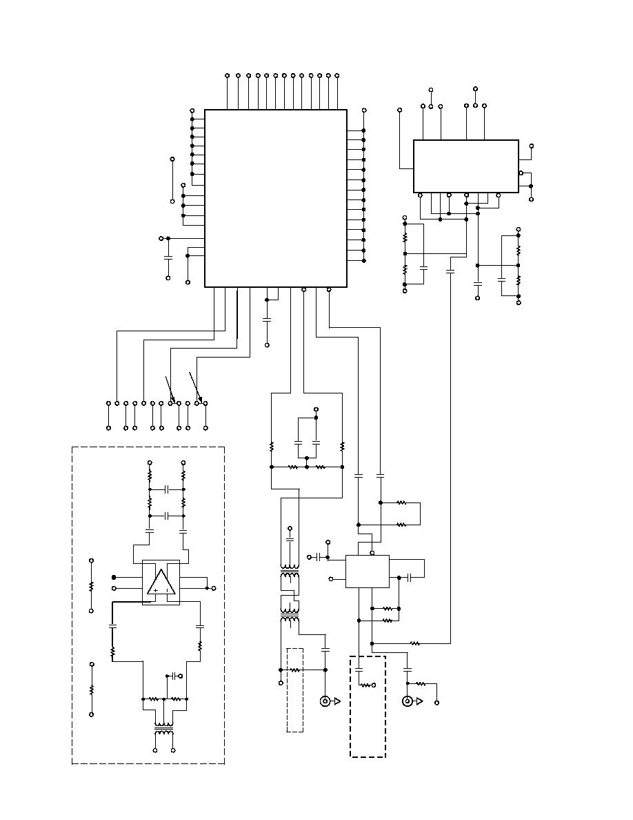
The schematic and layout of the evaluation board (Figures 13≠21)
represents a typical implementation of the AD9433. A multi-
layer board is recommended to achieve best results. It is highly
recommended that high quality, ceramic chip capacitors be used
to decouple each supply pin to ground directly at the device.
The pinout of the AD9433 facilitates ease of use in the implemen-
tation of high frequency, high resolution design practices. All of the
digital outputs and their supply and ground pin connections are
segregated to one side of the package, with the inputs on the
opposite side for isolation purposes.
Care should be taken when routing the digital output traces. To
prevent coupling through the digital outputs into the analog portion of
the AD9433 (V
CC
, AIN, and VREF), minimal capacitive loading
should be placed on these outputs.
It is recommended that a fan-out of only one gate should be used
for all AD9433 digital outputs.
The layout of the encode circuit is equally critical, and should
be treated as an analog input. Any noise received on this circuitry
will result in corruption in the digitization process and lower
overall performance. The Encode clock must be isolated from
the digital outputs and the analog inputs.
Replacing the AD9432 with the AD9433
The AD9433 is pin-compatible with the AD9432, although
there are two control pins on the AD9433 that do not connect
(DNC) and supply (V
CC
) connections on the AD9432. They are
summarized in the table below.
Table IV. AD9432/AD9433 Pin Differences
Pin
AD9432
AD9433
41
DNC
DFS
42
V
CC
SFDR MODE
Using the AD9433 in an AD9432 pin assignment will configure
the AD9433 as follows:
∑ The SFDR improvement circuit will be enabled.
∑ The DFS pin will float LOW, selecting two's complement
coding for the digital outputs, which is the same as the AD9432.
Table V summarizes differences between the AD9432 and
AD9433 analog and encode input common-mode voltages.
These inputs may be ac-coupled so that the devices can be used
interchangeably.
Table V. Other AD9432/AD9433 Differences
Attribute
AD9432
AD9433
ENCODE/
ENCODE V
COMMON MODE
1.6 V
3.75 V
AIN/
AIN V
COMMON MODE
3.0 V
4.0 V
Digital Outputs
The digital outputs are 3 V (2.7 V to 3.3 V) TTL/CMOS-
compatible for lower power consumption. The output data
format is selectable through the data format select (DFS)
CMOS input. DFS = 1 selects offset binary; DFS = 0 selects
two's complement coding.
Table II. Offset Binary Output Coding (DFS = 1, V
REF
= 2.5 V)
AIN ≠
AIN (V)
Digital
Code
Range = 2 V p-p
Output
4095
+1.000
1111 1111 1111
G
G
G
G
G
G
2048
0
1000 0000 0000
2047
≠0.00049
0111 1111 1111
G
G
G
G
G
G
0
≠1.000
0000 0000 0000
Table III. Two's Complement Output Coding (DFS = 0, V
REF
= 2.5 V)
AIN ≠
AIN (V)
Digital
Code
Range = 2 V p-p
Output
+2047
+1.000
0111 1111 1111
G
G
G
G
G
G
0
0
0000 0000 0000
≠1
≠0.00049
1111 1111 1111
G
G
G
G
G
G
≠2048
≠1.000
1000 0000 0000
Voltage Reference
A stable and accurate 2.5 V voltage reference is built into the
AD9433 (VREFOUT). In normal operation the internal reference
is used by strapping Pin 45 to Pin 46 and placing a 0.1 F
decoupling capacitor at VREFIN. The input range can be
adjusted by varying the reference voltage applied to the
AD9433. No appreciable degradation in performance occurs
when the reference is adjusted to 50. The full-scale range of the
ADC tracks reference voltage changes linearly.
Timing
The AD9433 provides latched data outputs, with 10 pipeline
delays. Data outputs are available one propagation delay (t
PD
)
after the rising edge of the encode command (see Timing Dia-
gram). The length of the output data lines and loads placed on
them should be minimized to reduce transients within the AD9433;
these transients can detract from the converter's dynamic per-
formance. The minimum guaranteed conversion rate of the
AD9433 is 10 MSPS. At internal clock rates below 10 MSPS,
dynamic performance may degrade.
REV. 0
AD9433
≠16≠
Table VI. Power Supply Connections for the AD9433 Evaluation Board
Connector
Pin
Designator
External Supply Required
Approximate Current Level
P42
P1, P3
GND
Ground
P2
≠5 V (Optional U10 Supply)
≠5 V
30 mA
P4
V
DL
+3 V
144 mA
P43
P1, P3
GND
Ground
P2
V
O
+3 V
10 mA
P4
V
CC
+5 V
325 mA Without U10
355 mA With U10
Evaluation Board
The AD9433 evaluation board offers designers an easy way to
evaluate device performance. The user must supply an analog
input signal, encode clock reference, and power supplies. The
digital outputs of the AD9433 are latched on the evaluation
board, and are available with a data ready signal at a 40-pin
edge connector. Please refer to the evaluation board schematic,
layout, and bill of materials that follow.
Power Connections
Power to the board is supplied via two detachable, four-pin
power strips (P42 and P43). These eight pins should be driven
as outlined in Table VI. Please note that the ≠5 V supply is
optional, and only required if the user adds differential op amp
U10 to the board.
Jumper Options
The table below describes the jumper options on the AD9433
Evaluation board.
Table VII. AD9433 Evaluation Board Jumper Options
Jumper
Designation
Connection
Configuration
SFDR
5 V
SFDR Enhancement
Circuit Enabled
GND
SFDR Enhancement
Circuit Disabled
DFS
5 V
Offset Binary Output
Data Format
GND
Two's Complement
Output Data Storage
LATCH
E10 to E6
Output Register (U7≠U8)
Clock is Buffered
E10 to E5
Output Register (U7≠U8)
Clock is Inverted
DATA READY
E7 to E8
Data Ready Signal is
Buffered
E7 to E9
Data Ready Signal is
Inverted
Encode Signal and Distribution
The encode input signal should drive SMB connector P38,
which has an on-board 50
termination. This signal is ac-coupled,
and may be either a low jitter pulse or a sine wave reference,
with up to 4 V p-p amplitude. U2 (MC10EP16) converts this
single-ended input signal to a differential PECL signal to drive
the AD9433. U1 (DS90LV048A) also converts the signal at P38
to a CMOS level signal to drive the clock inputs of the two out-
put data registers U7≠U8, (74LVT574WM), the reconstruction
DAC U3 (AD9772AAST), and the output data connector.
Analog Input
The analog input signal is ac-coupled to the evaluation board by
SMB connector P39. Transformers T1 and T2 (ADT1-1WT)
convert this signal to a differential signal to drive AIN and
AIN
of the AD9433. These RF transformers are specified as 1:1, but
their turns ratio is actually 6:7. T1 is rotated 180
∞ and mounted
on the board such that its secondary and primary are reversed,
making its ratio 7:6. The second transformer in series now form
a combined 1:1 turns ration for the analog signal, and provide a
50
termination for connector J1 via 25 resistors R3 and R4.
Resistor R3, normally omitted, can be used to terminate P39 if
the transformers are removed for single ended drive. In this
configuration, the user will need to short the input signal from
Pin 3 of T1 to Pin 6 of T2, and remove resistor R4. Resistor R3
should remain in place to match the impedance of AIN and
AIN.
Using the AD8350
An optional driver circuit for the analog input, based on the
AD8350 differential amplifier, is included in the layout of the
AD9433 evaluation board. This portion of the evaluation circuit
is not populated when the board is manufactured, but can be
easily added by the user. Removing resistors R29 and R30 will
disconnect the normal analog input signal path, and populating
R17 and R31 will connect the AD8350 output network.
DAC Reconstruction Circuit
The data available at output connector U2 is also reconstructed
by DAC U3, the AD772A. This 14-bit, high-speed digital-to-
analog converter is included as a tool in setting up and debugging the
evaluation board. It should not be used to measure the performance
of the AD9433, as its performance will not accurately reflect the
performance of the ADC. As configured on the AD9433 evaluation
board, the AD9772A divides the input clock frequency by a factor
of two, and ignores every other sample from the AD9433. The
AD9772 internally interpolates the missing samples so that the
DAC output will reflect the input of the AD9433 only when the
analog input frequency is less than or equal to 1/4 the ADC
encode rate. The AD9772 requires offset binary format so the
DFS jumper should be connected to 5 V. The DAC's output,
available at J1, will drive 50
. The user may move the jumper
wire between E43 and E42 to connect E43 to E44, thus activating
the SLEEP function of the DAC.

REV. 0
AD9433
≠17≠
Evaluation Board Bill of Materials
Item
Qty
Reference Designator
Device
Package
Value
1
1
AD9433/PCB
PCB
2
1
U4
ADC
QFP52
AD9433BST-XXX
3
1
U3
DAC
LQFP48
AD9772AAST
4
1
U1
Quad LVDS/CMOS
SO16
DS90LV048A
5
1
U2
Diff. ECL Receiver
SO8NB
MC10EP16
6
2
U7≠U8
D Flip-Flop
74LVT574WM
7
2
T1≠T2
1:1 Transformer
CD542
ADT1-1WT
8
35
C1, C2, C4≠C8, C10, C12≠C18,
Capacitor
0603A
0.1
µF
C20≠C24, C27≠C28, C30≠C38, C42≠
C43, C45, C48
9
3
C9, C40≠C41
Capacitor
BCAPTAJD
10
µF
10
1
C11
Capacitor
0603A
10
µF
11
2
R10, R23
BRES603
0603A
50
12
2
R29≠R30
BRES603
0603A
33
13
4
R1≠R2, R24≠R25
BRES603
0603A
510
14
3
R3≠R4, R7
BRES603
0603A
25
15
3
R6, R8, R14
BRES603
0603A
2 k
16
2
R9, R13
BRES603
0603A
1.2 k
17
2
R11, R16
BRES603
0603A
1 k
18
1
R12
BRES603
0603A
220
19
2
RZ1≠RZ2
Resistor Pack
SO16RES
742C163221 (220
)
20
2
RZ4≠RZ5
Resistor Pack
SO16RES
742C163220 (22
)
21
3
J1, P38≠P39
SMBPN
SMB
PC-Mount SMB
22
1
P44
40 Pin Header
C40MS
Samtec Tsw-120-07-G-D
23
2
P42≠P43
Power Connector
PTMICRO4
Weiland
Z5.531.3425.0 Posts
25.602.5453.0 Top
24
15
E5≠E7, E8≠E10, E19≠E21, E25≠E27,
"E" Holes
Jumper Blocks
TSW-120-07-G-S
E31≠E33
SMT-100-BK-G
25
4
E28/E29, E36/E37, E39/E40, E42/E43
"E" Holes
Wire Straps
Short at Assembly
26
*
1
T3
1:1 Transformer
CD543
ADT1-1WT
27
*
1
U10
Op Amp
SO8
AD8350
28
*
7
C3, C46≠C47, C50≠C53
Capacitor
0603A
0.1
µF
29
*
1
C44
Capacitor
BCAPTAJD
10
µF
30
*
2
R15, R27
BRES604
0603A
50
31
*
2
R18≠R19
BRES606
0603A
25
32
*
2
R20, R33
BRES608
0603A
1.5 k
33
*
2
R21, R28
BRES605
0603A
100
34
*
6
L1≠L2, R17, R22, R31, C29, C49
Select (R, L, C)
0603A
Select
35
*
1
P41
SMBPN
SMB
PC-Mount SMB
36
*
6
E30, E34≠E35, E38, E41, E44
"E" Holes
Option Holes
*Items are included in the PCB design, but are omitted at assembly.
REV. 0
AD9433
≠18≠
16
12
9
GND
V
DL
C14 0.1
F
R9
1.2k
R8
2k
GND
V
DL
R14
2k
GND
V
DL
C17
0.1
F
R13
1.2k
C16
0.1
F
GND
C15
0.1
F
1
4
5
8
2
3
6
7
V
DL
V
CC
IN1N
IN1P
IN2P
IN2N
IN3N
IN3P
IN4P
IN4N
OUT1
OUT2
OUT3
OUT4
15
14
11
10
13
E5
E6
E8
E9
E7
E10
LATCH
DR
GND
ENN
E
NP
DS90LV04BATM
U1
T1 ADT1-WT1
6
4
5
3
1
2
T2 ADT1-WT1
1
3
5
4
6
2
0.1
F
GND
PRI
SEC
PRI
SEC
GND
C24
V
CC
R4
R3
25
25
R29
33
R30
33
C10
C11
0.1
F
10pF
AIN
GND
ENC
ENC
C13 0.1
F
C1
0.1
F
GND
R1
510
R2
510
GND
C2
0.1
F
C8
2
3
45
6
7
8
CLK
CLKN
V
BB
V
EE
Q
Q
V
CC
U2
10EL16
1
A
R24
510
R25
510
R12
220
GND
GND
GND
P39
SMBMST
P38
SMBMST
R22
SELECT
R23
50
R15
50
C3
0.1
F
C4
0.1
F
C7
0.1
F
ANALOG
ENCODE
OPTIONAL
OPTIONAL
GND
P5
E19
E20
E27
E26
E30
E29
E33
E32
E21
E25
E28
E31
VC
C
VC
C
VC
C
VC
C
GND
GND
GND
GND
PAD UNDER PART
V
CC
OPTIONAL
ANALOG INPUT
IN+
OUT
≠
R33
1.5k
IN
≠
OUT+
R20
1.5k
T18
T1
T3
ADT1-WT1
1
3
5
4
6
2
R19
25
R18
25
GND
R21
100
R21
100
C52
100nF
C53
100nF
≠
5V
GND
OUT
≠
OUT+
12
3
4
87
6
5
IN
≠
IN+
GND
GND
ENBL
V
CC
U10
C51
C29
C49
L1
L2
R17
R31
AIN
AIN
AD8350
GND
C18
0.1
F
V
CC
GND
GND
V
DD
V
DD
V
DD
V
DD
V
CC
V
CC
V
CC
V
CC
V
CC
V
CC
V
CC
V
CC
V
CC
34
91
0
1
3
3
2
2
3
2
2
3
6
5
2
4
7
4
4
3
7
6
5
2
OR
(
MSB) D11
D10
D9
D8
D7
D6
D5
D4
D3
D2
D1
D0
OR
D11
D10
D9
D8
D7
D6
D5
D4
D3
D2
D1
D0
14
15
16
17
18
19
20
25
26
27
28
29
30
DGND
DGND
GND
GND
GND
GND
GND
GND
GND
GND
GND
DGND
DGND
12
31
24
21
33
11
35
51
48
43
38
4
3
1
ENC
ENC
AIN
AIN
VREFIN
VREFOUT
GAIN
SCLK
DFS
SFDR
7
8
50
49
46
45
39
40
41
42
GND
U4
GND
C6 0.1
F
GND
V
CC
V
O
AD9433QFP52
STRAPPED
TO GND
STRAPPED
TO GND
7:6
6
:7
C50
GND
Figure 13. Evaluation Board Schematic

REV. 0
AD9433
≠19≠
V
DL
GND
C42
0.1 F
C38
0.1 F
C34
0.1 F
C33
0.1 F
C12
0.1 F
48 47 46 45 44
39 38 37
43 42 41 40
36
35
34
33
32
31
30
29
28
27
26
25
STRAPPED TO
GROUND
STRAPPED TO
GROUND
GND
GND
VDL
VDL
E41
E40
E39
E38
E37
E36
J1
GND GND
R10
50
GND
GND
R7
25
R6
2k
GND
C5
0.1 F
GND
GND
E44
E42
E43
V
DL
GND
V
DL
GND
GND
GND
LATCH
V
DL
GND
GND
R16
1k
R11
1k
C43
0.1 F
13 14 15 16 17 18 19 20 21 22 23 24
DB3
DB2
DB1
DB0
MOD1
MOD0
DCOM
DCOM
DV
DD
DV
DD
NC
NC
1
2
3
4
5
6
7
8
9
10
11
12
DCOM
DCOM
DB13
DB12
DB11
DB10
DB9
DB8
DB7
DB6
DB5
DB4
DV
DD
DV
DD
AV
DD
AV
DD
ACOM
IOUTA
IOUTB
ACOM
FSADJ
REFIO
REFLO
ACOM
SLEEP
LPF
PLLV
DD
PLLCOM
CLKV
DD
CLKCOM
CLK+
CLK≠
DIV0
DIV1
RESET
PLLLOCK
VDL
VDL
GND
GND
V
DL
V
DL
V
DL
V
DL
GND
B11
B10
B9
B8
B7
B6
B5
B4
B3
B2
GND
GND
B1
B0
AD9772A
U3
NC = NO CONNECT
Figure 14. Evaluation Board Schematic

REV. 0
AD9433
≠20≠
20
19
18
17
16
15
14
13
12
11
1
2
3
4
5
6
7
8
9
10
U8
74AC574M
16
15
14
13
12
11
10
9
1
2
3
4
5
6
7
8
R1
R2
R3
R4
R5
R6
R7
R8
16
15
14
13
12
11
10
9
1
2
3
4
5
6
7
8
R1
R2
R3
R4
R5
R6
R7
R8
GND
GND
V
DL
LATCH
OUT
EN
D0
D1
D2
D3
D4
D5
D6
D7
GND
V
CC
Q0
Q1
Q2
Q3
Q4
Q5
Q6
Q7
CLOCK
R5016I50
RZ1
221
R5016I50
RZ1
220
D0
D1
D2
D3
D4
B4
B0
B1
B2
B3
A0
A1
A2
A3
A4
20
19
18
17
16
15
14
13
12
11
1
2
3
4
5
6
7
8
9
10
U7
74AC574M
16
15
14
13
12
11
10
9
1
2
3
4
5
6
7
8
R1
R2
R3
R4
R5
R6
R7
R8
16
15
14
13
12
11
10
9
1
2
3
4
5
6
7
8
R1
R2
R3
R4
R5
R6
R7
R8
GND
GND
V
DL
LATCH
OUT
EN
D0
D1
D2
D3
D4
D5
D6
D7
GND
V
CC
Q0
Q1
Q2
Q3
Q4
Q5
Q6
Q7
CLOCK
R5016I50
RZ1
221
R5016I50
RZ1
220
D5
D6
D7
D8
D9
D10
D11
OR
A5
A6
A7
A8
A9
A10
A11
ADR
B5
B6
B7
B8
B9
B10
B11
B0R
2
4
6
8
10
12
14
16
18
20
22
24
26
28
30
32
34
36
38
40
1
3
5
7
9
11
13
15
17
19
21
23
25
27
29
31
33
35
37
39
P44
C40M5
P2
P4
P6
P8
P10
P12
P14
P16
P18
P20
P22
P24
P26
P28
P30
P32
P34
P36
P38
P40
P1
P3
P5
P7
P9
P11
P13
P15
P17
P19
P21
P23
P25
P27
P29
P31
P33
P35
P37
P39
GND
B0R
B0
B1
B2
B3
B4
B5
B6
B7
B8
B9
B10
B11
DR
GND
GND
GND
GND
GND
GND
GND
GND
GND
GND
GND
GND
GND
GND
GND
GND
GND
GND
GND
GND
GND
1
2
3
4
P1
P2
P3
P4
GND
GND
V
DL
(+3V)
≠5V
P42 PTMICRO4
1
2
3
4
P1
P2
P3
P4
GND
GND
V
CC
(+5V)
V
O
(+3V)
P43 PTMICRO4
OPTIONAL
V
DL
V
D
E34
E35
C9
10 F
V
DL
GND
+
C20
C21
LATCHES ≠ 0.1 F
C48
0.1 F
V
CC
GND
C44
10 F
≠5V
GND
C47
0.1 F
+
OPTIONAL
C45
V
DL
GND
C22
C41
10 F
+
V
CC
GND
C30
C28
DUT BYPASS ≠ 0.1 F
C27
C23
C32
C31
C40
10 F
+
V
D
GND
C37
C36
C35
DUT BYPASS ≠ 0.1 F
R27
50
GND
DR
P41
5MBM5T
OPTIONAL
H1
MTHOLES
H2
MTHOLES
H3
MTHOLES
H4
MTHOLES
GND
Figure 15. Evaluation Board Schematic
REV. 0
AD9433
≠21≠
AD9433 EVALUATION BOARD LAYOUT
Figure 16. Top Silkscreen
Figure 17. Top Level Routing
Figure 18. Ground Plane
Figure 19. Power Plane
REV. 0
AD9433
≠22≠
Figure 20. Bottom Layer Routing
Figure 21. Bottom Silkscreen

REV. 0
AD9433
≠23≠
OUTLINE DIMENSIONS
Dimensions shown in inches and (mm).
Thermally Enhanced
52-Lead Power Thin Plastic Quad Flatpack (LQFP_ED)
(SQ-52)
0.026 (0.65)
0.015 (0.38)
0.013 (0.32)
0.009 (0.22)
0.472 (12.00) SQ
0.402 (10.20)
0.394 (10.00) SQ
0.386 (9.80)
TOP VIEW
(PINS DOWN)
40
52
1
14
13
26
27
39
0.307 (7.80)
0.063
(1.60)
MAX
VIEW A
SEATING
PLANE
0.030 (0.75)
0.024 (0.60)
0.018 (0.45)
0.006 (0.15)
0.002 (0.05)
VIEW A
0.004 (0.10)
COPLANARITY
0.057 (1.45)
0.055 (1.40)
0.053 (1.35)
40
52
1
14
13
26
27
39
EXPOSED
HEATSINK
(CENTERED)
0.093 (2.35)
0.087 (2.20)
0.081 (2.05)
(4 PLCS)
0.236 (6.00)
0.232 (5.90)
0.228 (5.80)
0.236 (6.00)
0.232 (5.90)
0.228 (5.80)
0.104 (2.65)
0.098 (2.50)
0.093 (2.35)
(4 PLCS)
BOTTOM VIEW
(PINS UP)
NOTES
1. CONTROLLING DIMENSIONS ARE IN MILLIMETERS. INCH DIMENSIONS ARE ROUNDED OFF MILLIMETER
EQUIVALENTS FOR REFERENCE ONLY AND ARE NOT APPROPRIATE FOR USE IN DESIGN.
2. ALTHOUGH NOT REQUIRED IN ALL APPLICATIONS, THE AD9433 HAS AN EXPOSED METALLIC PAD ON THE
PACKAGE BOTTOM WHICH IS INTENDED TO ENHANCE THE HEAT REMOVAL PATH. TO MAXIMIZE THE REMOVAL
OF HEAT, A LAND PATTERN WITH CLOSELY SPACED THERMAL VIAS TO THE GROUND PLANE(S) SHOULD
BE INCORPORATED ON THE PCB WITHIN THE FOOTPRINT OF THE PACKAGE CORRESPONDING TO THE
EXPOSED METAL PAD DIMENSIONS OF THE PACKAGE. THE SOLDERABLE LAND AREA SHOULD BE SOLDER
MASK DEFINED AND BE AT LEAST THE SAME SIZE AND SHAPE AS THE EXPOSED PAD AREA ON THE
PACKAGE. AT LEAST 0.25 MM CLEARANCE BETWEEN THE OUTER EDGES OF THE LAND PATTERN AND THE
INNER EDGES OF THE PAD PATTERN SHOULD BE MAINTAINED TO AVOID ANY SHORTS.

≠24≠
C01977≠.8≠10/01(0)
PRINTED IN U.S.A.