 | ÐлекÑÑоннÑй компоненÑ: AD9706 | СкаÑаÑÑ:  PDF PDF  ZIP ZIP |
AD9704/AD9705/AD9706/AD9707 8-, 10-, 12-, 14-Bit, 175 MSPS TxDAC® D/A Converters Preliminary Data Sheet (Rev. PrC)
8-, 10-, 12-, 14-Bit, 175 MSPS
TxDAC
®
D/A Converters
Preliminary Technical Data
AD9704/AD9705/AD9706/AD9707
Rev. PrC
Information furnished by Analog Devices is believed to be accurate and reliable.
However, no responsibility is assumed by Analog Devices for its use, nor for any
infringements of patents or other rights of third parties that may result from its use.
Specifications subject to change without notice. No license is granted by implication
or otherwise under any patent or patent rights of Analog Devices. Trademarks and
registered trademarks are the property of their respective owners.
One Technology Way, P.O. Box 9106, Norwood, MA 02062-9106, U.S.A.
Tel: 781.329.4700
www.analog.com
Fax: 781.326.8703
© 2006 Analog Devices, Inc. All rights reserved.
FEATURES
0
1
Pin-compatible Family
Low Power Member of Pin Compatible
TxDAC Product Family
Power Dissipation @ 3.3 V:
21 mW @ 10 MSPS
24 mW @ 25 MSPS
30 mW @ 50 MSPS
Sleep Mode: 5 mW @ 3.3 V
Supply Voltage: 1.7 V to 3.6 V
SFDR to Nyquist:
AD9707: 85 dBc @ 5 MHz Output
AD9707: 80 dBc @ 10 MHz Output
AD9707: 75 dBc @ 20 MHz Output
AD9707 SNR @ 10 MHz Output, 125 MSPS: TBD dB
Differential Current Outputs: 1 mA to 5 mA
Data Format: Twos Complement or Straight Binary
On-Chip 1.0 V Reference
CMOS Compatible Digital Interface
Edge-Triggered Latches
32-LEAD LFCSP PACKAGE FEATURES
Clock Input: Single-Ended and Differential
Output Common Mode: Adjustable 0 V to 1.2 V
Power-Down Mode: < 400
W @ 3.3 V (SPI Controllable)
Serial Peripheral Interface (SPI)
Self-calibration
32-Lead LFCSP Pb-Free Package
28-LEAD TSSOP PACKAGE FEATURES
Internal 500
Load Resistor
Internal 16k
Resistor to Set Full Scale Current Output
Clock Input: Single-Ended
28-Lead TSSOP Pb-Free Package
1
Protected by U.S. Patent Numbers 5568145, 5689257, and 5703519
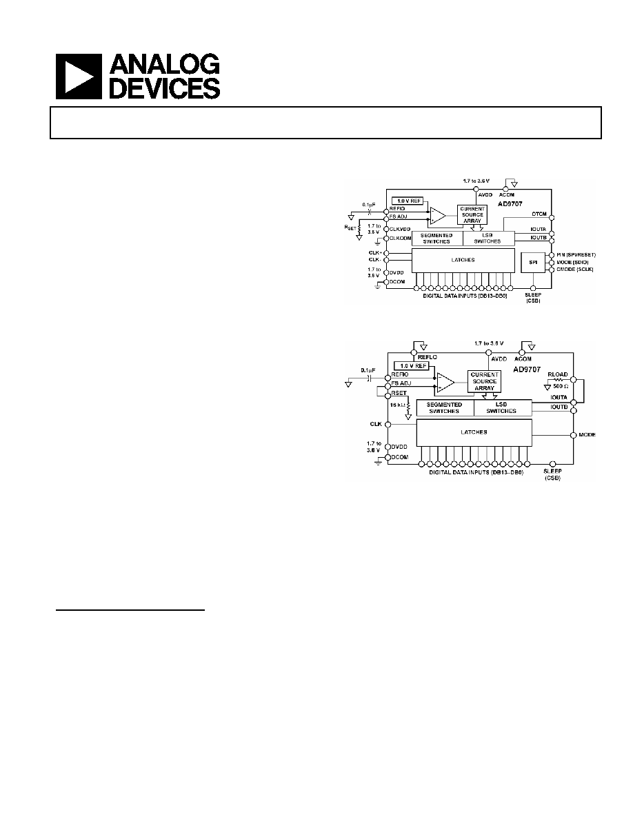
FUNCTIONAL BLOCK DIAGRAMS
Figure 1. AD9707 Functional Block Diagram (LFCSP Package)
Figure 2. AD9707 Functional Block Diagram (TSSOP Package)

AD9704/AD9705/AD9706/AD9707
Preliminary Technical Data
Rev. PrC | Page 2 of 32
GENERAL DESCRIPTION
The AD9704/05/06/07 are the fourth generation family in the
TxDAC series of high performance, CMOS digital-to-analog
converters (DACs). This pin compatible 8/10/12/14bit
resolution family has been optimized for low power operation
while maintaining excellent dynamic performance. The AD970x
family is pin compatible with the AD9748/40/42/44 family of
TxDAC converters and is specifically optimized for the transmit
signal path of communication systems. All of the devices share
the same interface, small outline package, and pinout, providing
an upward or downward component selection path based on
performance, resolution, and cost. The AD970X offers
exceptional ac and dc performance while supporting update
rates up to 175 MSPS.
The AD970X's flexible power supply operating range of 1.7 V to
3.6 V and low power dissipation makes it well suited for
portable and low power applications. Its power dissipation can
be further reduced to 15 mW with a slight degradation in
performance by lowering the full-scale current output. Also, a
power-down mode reduces the standby power dissipation to
approximately 5 mW.
The AD970X-LFCSP has an optional serial peripheral interface
(SPI) which provides a higher level of programmability to
enhance performance of the DAC. An adjustable output
common mode feature has also been added to the AD970X-
LFCSP that allows for easy interfacing to other components that
require common modes greater than 0 V.
Edge-triggered input latches and a 1.0 V temperature
compensated band gap reference have been integrated to
provide a complete monolithic DAC solution. The digital inputs
support 1.8 V and 3.3 V CMOS logic families.
PRODUCT HIGHLIGHTS
1. Pin Compatible: The AD970x line of TxDACs is pin
compatible with the AD974x TxDAC line.
2. Low power: Complete CMOS DAC operates on a single
supply of 3.6 V down to 1.7 V, consuming 25mW (3.3V)
and 10mW (1.8 V). The DAC full-scale current can be
reduced for lower power operation, and sleep and
power-down modes are provided for low power idle
periods.
3. Self-Calibration (foreground) enables true 14-bit INL
and DNL performance. (LFCSP only)
4. Data input supports twos complement or straight binary
data coding.
5. High speed, single-ended and differential (LFCSP only)
CMOS clock input supports 175 MSPS conversion rate.
6. SPI control offers higher level of programmability.
(LFCSP package only)
7. Adjustable output common mode from 0 V to 1.2 V
allows for easy interfacing to other components that
accept common mode levels greater than 0 V (LFCSP
only).
8. On-chip voltage reference: The AD970X includes a 1.0 V
temperature compensated band gap voltage reference.
9. Industry-standard 28-lead TSSOP and 32-lead LFCSP
packages.

Preliminary Technical Data
AD9704/AD9705/AD9706/AD9707
Rev. PrC | Page 3 of 32
TABLE OF CONTENTS
0H
FEATURES ...................................................................................
3 7H
1
1H
32-LEAD LFCSP PACKAGE FEATURES................................
3 8H
1
2H
28-LEAD TSSOP PACKAGE FEATURES ...............................
3 9H
1
3H
FUNCTIONAL BLOCK DIAGRAMS......................................
4 0H
1
4H
GENERAL DESCRIPTION .......................................................
4 1H
2
5H
PRODUCT HIGHLIGHTS ........................................................
4 2H
2
6H
AD9704/05/06/07Specifications ..................................................
4 3H
4
7H
DC Specifications (3.3 V) ...........................................................
4 4H
4
8H
Dynamic Specifications (3.3V) ..................................................
4 5H
6
9H
Digital Specifications (3.3V) ......................................................
4 6H
7
1 0H
DC Specifications (1.8V) ............................................................
4 7H
8
1 1H
Dynamic Specifications (1.8V) ................................................
4 8H
10
1 2H
Digital Specifications (1.8V) ....................................................
4 9H
11
1 3H
Absolute Maximum Ratings.........................................................
5 0H
12
1 4H
Thermal Characteristics ...........................................................
5 1H
12
1 5H
ESD Caution...............................................................................
5 2H
12
1 6H
Pin Configuration and Function Descriptions ..........................
5 3H
13
1 7H
Definitions of Specifications ........................................................
5 4H
17
1 8H
AD9707Typical Performance Characteristics .........................
5 5H
18
1 9H
Functional Description .................................................................
5 6H
21
2 0H
Serial Peripheral Interface (LFCSP only) ...............................
5 7H
21
2 1H
SPI Register Map .......................................................................
5 8H
23
2 2H
SPI Register Descriptions .........................................................
5 9H
23
2 3H
Reference Operation .................................................................
6 0H
24
2 4H
Reference Control Amplifier....................................................
6 1H
24
2 5H
DAC Transfer Function ............................................................
6 2H
24
2 6H
Analog Outputs..........................................................................
6 3H
25
2 7H
Adjustable Output Common Mode (LFCSP only) ...............
6 4H
26
2 8H
Digital Inputs .............................................................................
6 5H
26
2 9H
Clock Input.................................................................................
6 6H
26
3 0H
DAC Timing...............................................................................
6 7H
26
3 1H
Power Dissipation......................................................................
6 8H
27
3 2H
Evaluation Board ...........................................................................
6 9H
29
3 3H
General Description ..................................................................
7 0H
29
3 4H
Outline Dimensions ......................................................................
7 1H
30
3 5H
Ordering Guide..............................................................................
7 2H
31
3 6H
Revision History ............................................................................
7 3H
32

AD9704/AD9705/AD9706/AD9707
Preliminary Technical Data
Rev. PrC | Page 4 of 32
AD9704/05/06/07SPECIFICATIONS
DC SPECIFICATIONS (3.3 V)
(T
MIN
to T
MAX
, AVDD = 3.3 V, DVDD = 3.3 V, CLKVDD = 3.3 V, I
OUTFS
= 2 mA, unless otherwise noted.)
Table 1.
AD9707
AD9706
AD9705
AD9704
Parameter
Min Typ Max Min Typ
Max
Min Typ Max
Min Typ Max
Unit
RESOLUTION
14
Bits
DC ACCURACY
0 F
1
Integral Nonlinearity (INL) Pre-
calibration
±3
±0.5
±0.12 TBD
LSB
Integral Nonlinearity (INL) Post-
calibration
1 F
2
±0.8
±0.25 ±0.04 TBD
LSB
Differential Nonlinearity (DNL) Pre-
calibration
±1.5
±0.25 ±0.07 TBD
LSB
Differential Nonlinearity (DNL)
Post-calibration
2
±0.7
±0.13 ±0.03 TBD
LSB
ANALOG OUTPUT
Offset Error
-0.02
+0.02 -0.02
+0.02 -0.02
+0.02 -0.02
+0.02
% of FSR
Gain Error (Without Internal
Reference)
% of FSR
Gain Error (With Internal
Reference)
-0.8
-0.2 +0.2 -0.8
-0.2
+0.2
-0.8
-0.2
+0.2
-0.8
-0.2 +0.2
% of FSR
Full-Scale Output Current
2 F
3
1
2
5
1
2
5
1
2
5
1
2
5
mA
Output Compliance Range
-1
+1.25 -1
+1.25 -1
+1.25 -1
+1.25
V
Output Resistance
200
200
200
200
M
Output Capacitance
5
5
5
5
pF
REFERENCE OUTPUT
Reference Voltage
1.0
1.0
1.0
1.0
V
Reference Output Current
3 F
4
100
100
100
100
nA
REFERENCE INPUT
Input Compliance Range
0.1
1.25 0.1
1.25
0.1
1.25
0.1
1.25
V
Reference Input Resistance (Ext.
Reference)
1
1
1
1
M
Small Signal Bandwidth
0.5
0.5
0.5
0.5
MHz
TEMPERATURE
COEFFICIENTS
Offset Drift
0
0
0
0
ppm of
FSR/°C
Gain Drift (Without Internal
Reference)
TBD
TBD
TBD
TBD
ppm of
FSR/°C
Gain Drift (With Internal
Reference)
± 70
± 70
± 70
± 70
ppm of
FSR/°C
Reference Voltage Drift
± 80
± 80
± 80
± 80
ppm/°C
POWER
SUPPLY
Supply Voltages
AVDD
2.5
3.3
3.6
2.5
3.3
3.6
2.5
3.3
3.6
2.5
3.3
3.6
V
DVDD
2.5
3.3
3.6
2.5
3.3
3.6
2.5
3.3
3.6
2.5
3.3
3.6
V
CLKVDD
2.5
3.3
3.6
2.5
3.3
3.6
2.5
3.3
3.6
2.5
3.3
3.6
V
Analog Supply Current (I
AVDD
)
4.5
4.5
4.5
4.5
mA
Digital Supply Current (I
DVDD
)
4 F
5
1.1
1.1
1.1
1.1
mA
Clock Supply Current (I
CLKVDD
)
1.7
1.7
1.7
1.7
mA
Supply Current Sleep Mode (I
AVDD
)
0.4
1.0
0.4
1.0
0.4
1.0
0.4
1.0 mA
Supply Current Power-Down
Mode
20
20
20
20
A

Preliminary Technical Data
AD9704/AD9705/AD9706/AD9707
Rev. PrC | Page 5 of 32
Power Dissipation
7 4H
5
24
24
24
24
mW
Power Dissipation
5 F
6
46
46
46
46
mW
Power Supply Rejection Ratio--
AVDD
6F
7
-1
+1
-1
+1
-1
+1
-1
+1
% of
FSR/V
Power Supply Rejection Ratio--
DVDD
75H
7
-0.04
+0.04 -0.04
+0.04 -0.04
+0.04 -0.04
+0.04
% of
FSR/V
OPERATING RANGE
-40
+85
-40
+85
-40
+85
-40
+85
°C
1
Measured at IOUTA, driving a virtual ground.
2
Calibration offered in LFCSP package only.
3
Nominal full-scale current, I
OUTFS
, is 32 times the I
REF
current.
4
An external buffer amplifier with input bias current <100 nA should be used to drive any external load.
5
Measured at f
CLOCK
= 25 MSPS and f
OUT
= 2.5 MHz.
6
Measured at f
CLOCK
= 175 MSPS and f
OUT
= 20 MHz.
7
±5% power supply variation.
Document Outline
- þÿ
- þÿ
- þÿ
- þÿ
- þÿ
- þÿ
- þÿ
- þÿ
- þÿ
- þÿ
- þÿ
- þÿ
- þÿ
- þÿ
- þÿ
- þÿ
- þÿ
- þÿ
- þÿ
- þÿ
- þÿ
- þÿ
- þÿ
- þÿ
- þÿ
- þÿ
- þÿ
- þÿ
- þÿ
- þÿ
- þÿ
- þÿ
- þÿ
- þÿ