 | ÐлекÑÑоннÑй компоненÑ: AD9709 | СкаÑаÑÑ:  PDF PDF  ZIP ZIP |
Äîêóìåíòàöèÿ è îïèñàíèÿ www.docs.chipfind.ru
REV. 0
Information furnished by Analog Devices is believed to be accurate and
reliable. However, no responsibility is assumed by Analog Devices for its
use, nor for any infringements of patents or other rights of third parties
which may result from its use. No license is granted by implication or
otherwise under any patent or patent rights of Analog Devices.
a
AD9709*
One Technology Way, P.O. Box 9106, Norwood, MA 02062-9106, U.S.A.
Tel: 781/329-4700
World Wide Web Site: http://www.analog.com
Fax: 781/326-8703
© Analog Devices, Inc., 2000
8-Bit, 125 MSPS
Dual TxDAC+
®
D/A Converter
PRODUCT DESCRIPTION
The AD9709 is a dual-port, high-speed, two-channel, 8-bit
CMOS DAC. It integrates two high-quality 8-bit TxDAC+
cores, a voltage reference, and digital interface circuitry into a
small 48-lead LQFP package. The AD9709 offers exceptional
ac and dc performance while supporting update rates up to
125 MSPS.
The AD9709 has been optimized for processing I and Q data in
communications applications. The digital interface consists of
two double-buffered latches as well as control logic. Separate
write inputs allow data to be written to the two DAC ports
independent of one another. Separate clocks control the update
rate of the DACs.
A mode control pin allows the AD9709 to interface to two sep-
arate data ports, or to a single interleaved high-speed data port.
In interleaving mode, the input data stream is demuxed into
its original I and Q data and then latched. The I and Q data
is then converted by the two DACs and updated at half the
input data rate.
The GAINCTRL pin allows two modes for setting the full-scale
current (I
OUTFS
) of the two DACs. I
OUTFS
for each DAC can be
set independently using two external resistors, or I
OUTFS
for
both DACs can be set using a single external resistor.
The DACs utilize a segmented current source architecture
combined with a proprietary switching technique to reduce
glitch energy and to maximize dynamic accuracy. Each DAC
provides differential current output thus supporting single-ended
or differential applications. Both DACs can be simultaneously
updated and provide a nominal full-scale current of 20 mA.
The full-scale currents between each DAC are matched to
within 0.1%.
The AD9709 is manufactured on an advanced low-cost CMOS
process. It operates from a single supply of 3.0 V to 5.0 V and
consumes 380 mW of power.
PRODUCT HIGHLIGHTS
1. The AD9709 is a member of a pin-compatible family of dual
TxDACs providing 8-, 10-, 12-, and 14-bit resolution.
2. Dual 8-Bit, 125 MSPS DACs: A pair of high-performance
DACs optimized for low-distortion performance provide for
flexible transmission of I and Q information.
3. Matching: Gain matching is typically 0.1% of full-scale, and
offset error is better than 0.02%.
4. Low Power: Complete CMOS Dual DAC function operates
on 380 mW from a 3.0 V to 5.0 V single supply. The DAC
full-scale current can be reduced for lower power operation,
and a sleep mode is provided for low-power idle periods.
5. On-Chip Voltage Reference: The AD9709 includes a 1.20 V
temperature-compensated bandgap voltage reference.
6. Dual 8-Bit Inputs: The AD9709 features a flexible dual-port
interface allowing dual or interleaved input data.
FEATURES
8-Bit Dual Transmit DAC
125 MSPS Update Rate
Excellent SFDR to Nyquist @ 5 MHz Output = 66 dBc
Excellent Gain and Offset Matching: 0.1%
Fully Independent or Single Resistor Gain Control
Dual Port or Interleaved Data
On-Chip 1.2 V Reference
Single 5 V or 3 V Supply Operation
Power Dissipation: 380 mW @ 5 V
Power-Down Mode: 50 mW @ 5 V
48-Lead LQFP
APPLICATIONS
Communications
Basestations
Digital Synthesis
Quadrature Modulation
3D Ultrasound
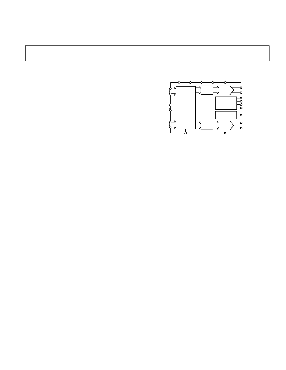
FUNCTIONAL BLOCK DIAGRAM
"1"
LATCH
"1"
DAC
REFIO
FSADJ1
FSADJ2
GAINCTRL
REFERENCE
BIAS
GENERATOR
I
OUTA1
I
OUTB1
SLEEP
I
OUTA2
I
OUTB2
DIGITAL
INTERFACE
AD9709
PORT1
PORT2
WRT1
WRT2
DVDD
DCOM
AVDD
ACOM
CLK1
CLK2
MODE
"2"
DAC
"2"
LATCH
TxDAC+ is a registered trademark of Analog Devices, Inc.
*Patent pending.

REV. 0
2
AD9709SPECIFICATIONS
DC SPECIFICATIONS
Parameter
Min
Typ
Max
Unit
RESOLUTION
8
Bits
DC ACCURACY
1
Integral Linearity Error (INL)
0.5
±0.1
+0.5
LSB
Differential Nonlinearity (DNL)
0.5
±0.1
+0.5
LSB
ANALOG OUTPUT
Offset Error
0.02
+0.02
% of FSR
Gain Error (Without Internal Reference)
2
±0.25
+2
% of FSR
Gain Error (With Internal Reference)
5
±1
+5
% of FSR
Gain Match
T
A
= 25
°C
0.3
±0.1
+0.3
% of FSR
T
MIN
to T
MAX
1.6
+1.6
% of FSR
T
MIN
to T
MAX
0.14
+0.14
dB
Full-Scale Output Current
2
2.0
20.0
mA
Output Compliance Range
1.0
+1.25
V
Output Resistance
100
k
Output Capacitance
5
pF
REFERENCE OUTPUT
Reference Voltage
1.14
1.20
1.26
V
Reference Output Current
3
100
nA
REFERENCE INPUT
Input Compliance Range
0.1
1.25
V
Reference Input Resistance
1
M
Small Signal Bandwidth
0.5
MHz
TEMPERATURE COEFFICIENTS
Offset Drift
0
ppm of FSR/
°C
Gain Drift (Without Internal Reference)
±50
ppm of FSR/
°C
Gain Drift (With Internal Reference)
±100
ppm of FSR/
°C
Reference Voltage Drift
±50
ppm/
°C
POWER SUPPLY
Supply Voltages
AVDD
3
5
5.5
V
DVDD
2.7
5
5.5
V
Analog Supply Current (IAVDD)
71
75
mA
Digital Supply Current (IDVDD)
4
5
7
mA
Digital Supply Current (IDVDD)
5
15
mA
Supply Current Sleep Mode (IAVDD)
8
12
mA
Power Dissipation
4
(5 V, I
OUTFS
= 20 mA)
380
410
mW
Power Dissipation
5
(5 V, I
OUTFS
= 20 mA)
420
450
mW
Power Dissipation
6
(5 V, I
OUTFS
= 20 mA)
450
mW
Power Supply Rejection Ratio
7
--AVDD
0.4
+0.4
% of FSR/V
Power Supply Rejection Ratio
7
--DVDD
0.025
+0.025
% of FSR/V
OPERATING RANGE
40
+85
°C
NOTES
1
Measured at I
OUTA
, driving a virtual ground.
2
Nominal full-scale current, I
OUTFS
, is 32 times the I
REF
current.
3
An external buffer amplifier with input bias current <100 nA should be used to drive any external load.
4
Measured at f
CLOCK
= 25 MSPS and f
OUT
= 1.0 MHz.
5
Measured at f
CLOCK
= 100 MSPS and f
OUT
= 1 MHz.
6
Measured as unbuffered voltage output with I
OUTFS
= 20 mA and 50
R
LOAD
at I
OUTA
and I
OUTB
, f
CLOCK
= 100 MSPS and f
OUT
= 40 MHz.
7
±10% power supply variation.
Specifications subject to change without notice.
(T
MIN
to T
MAX
, AVDD = 5 V, DVDD = 5 V, I
OUTFS
= 20 mA, unless otherwise noted)

REV. 0
3
AD9709
DYNAMIC SPECIFICATIONS
Parameter
Min
Typ
Max
Unit
DYNAMIC PERFORMANCE
Maximum Output Update Rate (f
CLOCK
)
125
MSPS
Output Settling Time (t
ST
) (to 0.1%)
1
35
ns
Output Propagation Delay (t
PD
)
1
ns
Glitch Impulse
5
pV-s
Output Rise Time (10% to 90%)
1
2.5
ns
Output Fall Time (90% to 10%)
1
2.5
ns
Output Noise (I
OUTFS
= 20 mA)
50
pA/
Hz
Output Noise (I
OUTFS
= 2 mA)
30
pA/
Hz
AC LINEARITY
Spurious-Free Dynamic Range to Nyquist
f
CLOCK
= 100 MSPS; f
OUT
= 1.00 MHz
0 dBFS Output
63
68
dBc
6 dBFS Output
62
dBc
12 dBFS Output
56
dBc
18 dBFS Output
50
dBc
f
CLOCK
= 65 MSPS; f
OUT
= 1.00 MHz
68
dBc
f
CLOCK
= 65 MSPS; f
OUT
= 2.51 MHz
68
dBc
f
CLOCK
= 65 MSPS; f
OUT
= 5.02 MHz
66
dBc
f
CLOCK
= 65 MSPS; f
OUT
= 14.02 MHz
60
dBc
f
CLOCK
= 65 MSPS; f
OUT
= 25 MHz
50
dBc
f
CLOCK
= 125 MSPS; f
OUT
= 25 MHz
63
dBc
f
CLOCK
= 125 MSPS; f
OUT
= 40 MHz
55
dBc
Signal to Noise and Distortion Ratio
f
CLOCK
= 50 MHz; f
OUT
= 1 MHz
50
dB
Total Harmonic Distortion
f
CLOCK
= 100 MSPS; f
OUT
= 1.00 MHz
67
63
dBc
f
CLOCK
= 50 MSPS; f
OUT
= 2.00 MHz
63
dBc
f
CLOCK
= 125 MSPS; f
OUT
= 4.00 MHz
63
dBc
f
CLOCK
= 125 MSPS; f
OUT
= 10.00 MHz
63
dBc
Multitone Power Ratio (Eight Tones at 110 kHz Spacing)
f
CLOCK
= 65 MSPS; f
OUT
= 2.00 MHz to 2.99 MHz
0 dBFS Output
58
dBc
6 dBFS Output
51
dBc
12 dBFS Output
46
dBc
18 dBFS Output
41
dBc
Channel Isolation
f
CLOCK
= 125 MSPS; f
OUT
= 10 MHz
85
dBc
f
CLOCK
= 125 MSPS; f
OUT
= 40 MHz
77
dBc
NOTES
1
Measured single-ended into 50
load.
Specifications subject to change without notice.
(T
MIN
to T
MAX
, AVDD = 5 V, DVDD = 5 V, I
OUTFS
= 20 mA, Differential Transformer-Coupled Output,
50
Doubly Terminated, unless otherwise noted)
REV. 0
4
AD9709SPECIFICATIONS
CAUTION
ESD (electrostatic discharge) sensitive device. Electrostatic charges as high as 4000 V readily
accumulate on the human body and test equipment and can discharge without detection.
Although the AD9709 features proprietary ESD protection circuitry, permanent damage may
occur on devices subjected to high-energy electrostatic discharges. Therefore, proper ESD
precautions are recommended to avoid performance degradation or loss of functionality.
WARNING!
ESD SENSITIVE DEVICE
DIGITAL SPECIFICATIONS
Parameter
Min
Typ
Max
Unit
DIGITAL INPUTS
Logic "1" Voltage @ DVDD = 5 V
3.5
5
V
Logic "1" @ DVDD = 3
2.1
3
V
Logic "0" Voltage @ DVDD = 5 V
0
1.3
V
Logic "0" @ DVDD = 3
0
0.9
V
Logic "1" Current
10
+10
µA
Logic "0" Current
10
+10
µA
Input Capacitance
5
pF
Input Setup Time (t
S
)
2.0
ns
Input Hold Time (t
H
)
1.5
ns
Latch Pulsewidth (t
LPW
, t
CPW
)
3.5
ns
Specifications subject to change without notice.
ABSOLUTE MAXIMUM RATINGS
*
With
Parameter
Respect to
Min
Max
Unit
AVDD
ACOM
0.3
+6.5
V
DVDD
DCOM
0.3
+6.5
V
ACOM
DCOM
0.3
+0.3
V
AVDD
DVDD
6.5
+6.5
V
MODE, CLK1, CLK2, WRT1, WRT2
DCOM
0.3
DVDD + 0.3
V
Digital Inputs
DCOM
0.3
DVDD + 0.3
V
IOUTA1/IOUTA2, IOUTB1/IOUTB2
ACOM
1.0
AVDD + 0.3
V
REFIO, FSADJ1, FSADJ2
ACOM
0.3
AVDD + 0.3
V
GAINCTRL, SLEEP
ACOM
0.3
AVDD + 0.3
V
Junction Temperature
150
°C
Storage Temperature
65
+150
°C
Lead Temperature (10 sec)
300
°C
*Stresses above those listed under Absolute Maximum Ratings may cause permanent damage to the device. This is a stress rating only; functional operation of the
device at these or any other conditions above those indicated in the operational sections of this specification is not implied. Exposure to absolute maximum ratings for
extended periods may affect device reliability.
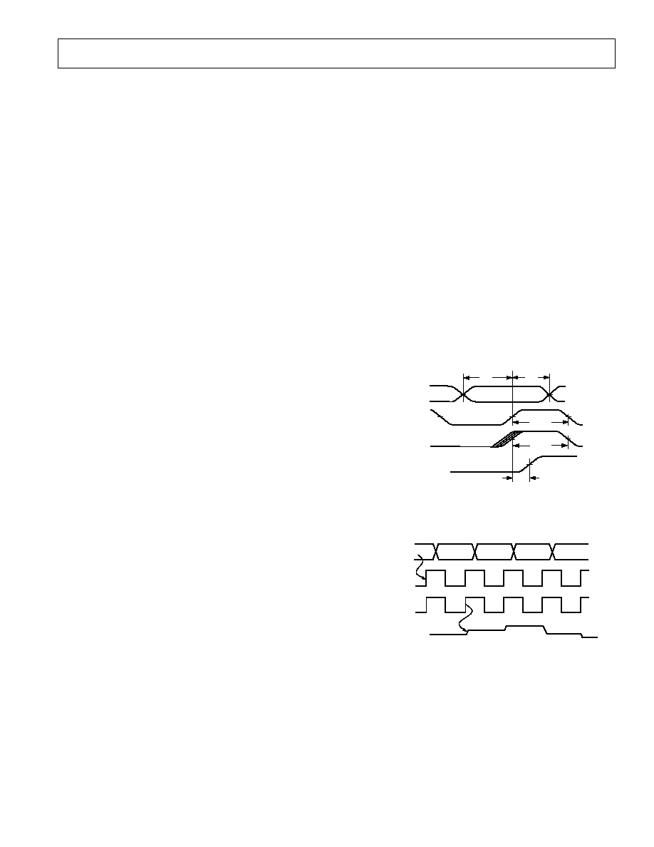
DATA IN
(WRT2) (WRT1 / IQWRT)
(CLK2) (CLK1/ IQCLK)
IOUTA
OR
IOUTB
t
LPW
t
PD
t
S
t
H
t
CPW
Figure 1. Timing Diagram for Dual and Interleaved Modes
(T
MIN
to T
MAX
, AVDD = 5 V, DVDD = 5 V, I
OUTFS
= 20 mA, unless otherwise noted)
ORDERING GUIDE
Temperature
Package
Package
Model
Range
Description
Option
AD9709AST
40
°C to +85°C Thin Plastic Quad ST-48
Flatpack (LQFP)
AD9709-EB
Evaluation Board
THERMAL CHARACTERISTICS
Thermal Resistance
48-Lead LQFP
JA
= 91
°C/W
See Dynamic and Digital sections for timing specifications.
REV. 0
AD9709
5
PIN FUNCTION DESCRIPTIONS
Pin No.
Name
Description
18
PORT1
Data Bits DB7P1 to DB0P1
914, 3136
NC
No Connection
15, 21
DCOM1, DCOM2
Digital Common
16, 22
DVDD1, DVDD2
Digital Supply Voltage
17
WRT1/IQWRT
Input Write Signal for PORT 1 (IQWRT in Interleaving Mode)
18
CLK1/IQCLK
Clock Input for DAC1 (IQCLK in Interleaving Mode)
19
CLK2/IQRESET
Clock Input for DAC2 (IQRESET in Interleaving Mode)
20
WRT2/IQSEL
Input Write Signal for PORT 2 (IQSEL in Interleaving Mode)
2330
PORT2
Data Bits DB7P2 to DB0P2
37
SLEEP
Power-Down Control Input
38
ACOM
Analog Common
39, 40
I
OUTA2
, I
OUTB2
"PORT 2" Differential DAC Current Outputs
41
FSADJ2
Full-Scale Current Output Adjust for DAC2
42
GAINCTRL
Master/Slave Resistor Control Mode
43
REFIO
Reference Input/Output
44
FSADJ1
Full-Scale Current Output Adjust for DAC1
45, 46
I
OUTB1
, I
OUTA1
"PORT 1" Differential DAC Current Outputs
47
AVDD
Analog Supply Voltage
48
MODE
Mode Select (1 = Dual Port, 0 = Interleaved)
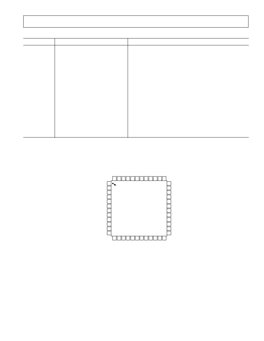
PIN CONFIGURATION
NC
NC
NC
NC
DB0-P1
DB1-P1
DB2-P1
DB3-P1
DB4-P1
DB5-P1
DB6-P1
DB7-P1(MSB)
NC
NC
NC
NC
NC
NC
DB1-P2
DB2-P2
DB3-P2
DB4-P2
DB5-P2
DB0-P2
AD9709
DUAL 8-BIT DAC
48-PIN LQFP
12
11
10
9
8
7
6
5
4
3
2
1
26
27
28
29
30
31
32
33
34
35
36
25
24
23
22
21
20
19
18
17
16
15
14
13
37
38
39
40
41
42
43
44
45
46
47
48
PIN 1
IDENTIFIER
MODE
AVDD
I
OUTA1
I
OUTB1
FSADJ1
REFIO
GAIN CTRL
FSADJ2
I
OUTB2
I
OUTA2
ACOM
SLEEP
NC
NC
DCOM1
DVDD1
WRT1/IQWRT
CLK1/IQCLK
CLK2/IQRESET
WRT/IQSEL
DCOM2
DVDD2
DB7-P2 (MSB)
DB6-P2
NC = NO CONNECT
REV. 0
AD9709
6
DEFINITIONS OF SPECIFICATIONS
Linearity Error (Also Called Integral Nonlinearity or INL)
Linearity error is defined as the maximum deviation of the
actual analog output from the ideal output, determined by a
straight line drawn from zero to full-scale.
Differential Nonlinearity (or DNL)
DNL is the measure of the variation in analog value, normalized
to full-scale, associated with a 1 LSB change in digital input code.
Monotonicity
A D/A converter is monotonic if the output either increases or
remains constant as the digital input increases.
Offset Error
The deviation of the output current from the ideal of zero is
called offset error. For I
OUTA
, 0 mA output is expected when
the inputs are all 0s. For I
OUTB
, 0 mA output is expected when
all inputs are set to 1s.
Gain Error
The difference between the actual and ideal output span. The
actual span is determined by the output when all inputs are set
to 1s minus the output when all inputs are set to 0s.
Output Compliance Range
The range of allowable voltage at the output of a current-output
DAC. Operation beyond the maximum compliance limits may
cause either output stage saturation or breakdown resulting in
nonlinear performance.
AVDD
DIGITAL
DATA
DB0-DB7
GAINCTRL
50
DVDD
DCOM
RETIMED CLOCK OUTPUT
LECROY 9210
PULSE
GENERATOR
TEKTRONIX
AWG-2021
w/OPTION 4
WRT1/
IQWRT
1.2V REF
R
SET
2
2k
CHANNEL 1 LATCH
CHANNEL 2 LATCH
PMOS
CURRENT
SOURCE
ARRAY
PMOS
CURRENT
SOURCE
ARRAY
SEGMENTED
SWITCHES
FOR DAC1
SEGMENTED
SWITCHES FOR
DAC2
LSB
SWITCH
LSB
SWITCH
MULTIPLEXING LOGIC
AD9709
DCOM ACOM
MODE
I
OUTA1
I
OUTB1
SLEEP
CLK2/
IQRESET
CLK1/
IQCLK
5V
FSADJ1
R
SET
1
2k
REFIO
0.1 F
FSADJ2
DB0-DB7
WRT2/
IQSEL
50
5V
MINI CIRCUITS
T1-1T
TO HP3589A
SPECTRUM/
NETWORK
ANALYZER
*AWG2021 CLOCK RETIMED SUCH THAT DIGITAL DATA TRANSITIONS
ON FALLING EDGE OF 50% DUTY CYCLE CLOCK
DVDD
DAC2
LATCH
DAC1
LATCH
CLK
DIVIDER
50
I
OUTA2
I
OUTB2
Figure 2. Basic AC Characterization Test Setup for AD9709, Testing Port 1 in Dual Port Mode, Using Independent
GAINCTRL Resistors on FSADJ1 and FSADJ2
Temperature Drift
Temperature drift is specified as the maximum change from the
ambient (25
°C) value to the value at either T
MIN
or T
MAX
. For
offset and gain drift, the drift is reported in ppm of full-scale
range (FSR) per degree C. For reference drift, the drift is
reported in ppm per degree C.
Power Supply Rejection
The maximum change in the full-scale output as the supplies
are varied from nominal to minimum and maximum specified
voltages.
Settling Time
The time required for the output to reach and remain within a
specified error band about its final value, measured from the
start of the output transition.
Glitch Impulse
Asymmetrical switching times in a DAC give rise to undesired
output transients that are quantified by a glitch impulse. It is
specified as the net area of the glitch in pV-s.
Spurious-Free Dynamic Range
The difference, in dB, between the rms amplitude of the output
signal and the peak spurious signal over the specified bandwidth.
Total Harmonic Distortion
THD is the ratio of the rms sum of the first six harmonic
components to the rms value of the measured input signal. It
is expressed as a percentage or in decibels (dB).
REV. 0
AD9709
7
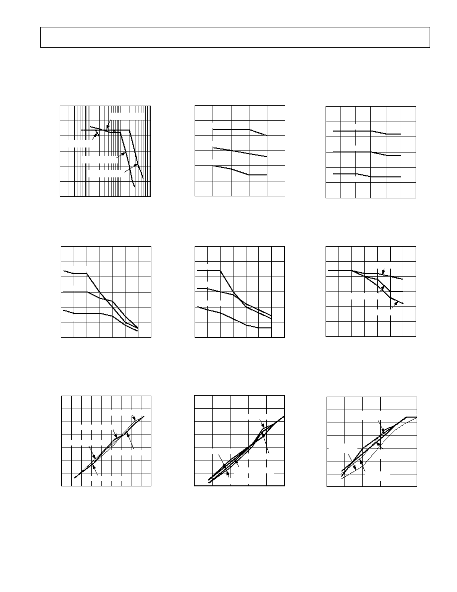
Typical Characterization Curves
(AVDD = 5 V, DVDD = 3.3 V, I
OUTFS
= 20 mA, 50
Doubly Terminated Load, Differential Output, T
A
= 25 C, SFDR up to Nyquist, unless
otherwise noted)
SFDR
dBc
75
70
60
65
45
1
10
100
f
OUT
MHz
0.1
50
55
f
CLK
= 5MSPS
f
CLK
= 65MSPS
f
CLK
= 125MSPS
f
CLK
= 25MSPS
Figure 3. SFDR vs. f
OUT
@ 0 dBFS
12dBFS
f
OUT
MHz
SFDR
dBc
45
0
5
25
10
15
20
70
65
60
55
50
30
35
0dBFS
6dBFS
75
Figure 6. SFDR vs. f
OUT
@ 65 MSPS
A
OUT
dBFS
SFDR
dBc
2
5MSPS /0.46MHz
25
19
7
65
40
50
45
55
60
16
70
22
13 10
4
1
75
10MSPS/0.91MHz
25MSPS/2.27MHz
65MSPS/5.91MHz
125MSPS/11.37MHz
Figure 9. Single-Tone SFDR vs. A
OUT
@ f
OUT
= f
CLOCK
/11
SFDR
dBc
0
2.5
0.5
1
1.5
2
70
55
50
45
0 dBFS
6 dBFS
12 dBFS
75
f
OUT
MHz
65
60
Figure 4. SFDR vs. f
OUT
@ 5 MSPS
f
OUT
MHz
SFDR
dBc
45
0
10
50
20
30
40
75
70
65
55
50
60
60
70
0dBFS
6dBFS
12dBFS
Figure 7. SFDR vs. f
OUT
@ 125 MSPS
A
OUT
dBFS
SFDR
dBc
45
0
20
15
5
65
50
55
40
60
70
10
5MSPS/1.0MHz
75
25
10MSPS/2.0MHz
25MSPS/5.0MHz
65MSPS/13.0MHz
125MSPS/5.0MHz
Figure 10. Single-Tone SFDR vs. A
OUT
@ f
OUT
= f
CLOCK
/5
f
OUT
MHz
SFDR
dBc
0
2
12
4
6
8
10
65
60
55
45
50
0dBFS
6dBFS
12dBFS
70
75
Figure 5. SFDR vs. f
OUT
@ 25 MSPS
f
OUT
MHz
SFDR
dBc
50
0
10
20
30
75
70
60
55
65
5
15
25
I
OUT FS
= 5mA
I
OUT FS
= 10mA
I
OUT FS
= 20mA
45
35
Figure 8. SFDR vs. f
OUT
and I
OUTFS
@ 65 MSPS and 0 dBFS
A
OUT
dBFS
SFDR
dBc
75
0
20
10
5
55
40
50
60
15
45
3.3/3.4MHz
@25MSPS
8.8/9.8MHz
@65MSPS
25
65
70
0.965/1.035MHz
@7MSPS
16.9/18.1Mz
@125MSPS
Figure 11. Dual-Tone SFDR vs. A
OUT
@ f
OUT
= f
CLOCK
/7
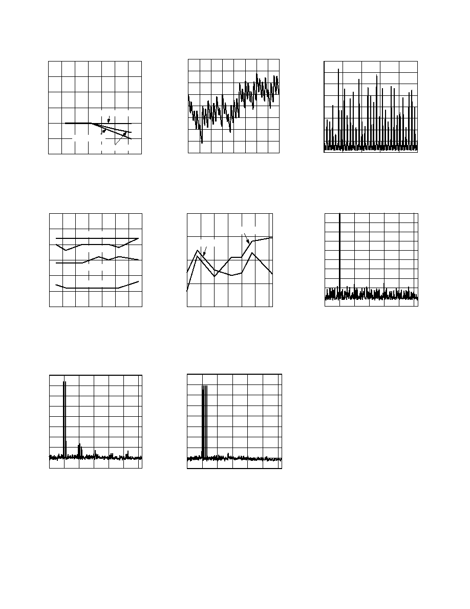
REV. 0
AD9709
8
f
CLK
MSPS
SINAD
dBc
40
20
140
40
60
80
100
120
55
60
65
I
OUTFS
= 5mA
70
45
50
0
I
OUTFS
= 10mA
I
OUTFS
= 20mA
Figure 12. SINAD vs. f
CLOCK
and I
OUTFS
@ f
OUT
= 5 MHz and 0 dBFS
TEMPERATURE C
SFDR
dBc
70
65
30
10
70
50
60
55
50
30
10
45
90
50
75
f
OUT
= 10MHz
f
OUT
= 25MHz
f
OUT
= 40MHz
f
OUT
= 60MHz
Figure 15. SFDR vs. Temperature @
f
CLK
= 125 MSPS, 0 dBFS
FREQUENCY MHz
AMPLITUDE
dBm
40
20
0
90
80
70
60
50
40
30
20
10
0
10
30
50
60
Figure 18. Dual-Tone SFDR @
f
CLK
= 125 MSPS
CODE
DNL
LSBs
0.01
0
50
0.01
0
0.07
0.06
0.05
0.04
0.03
0.02
100
150
200
250
Figure 14. Typical DNL
AMPLITUDE
dBm
FREQUENCY MHz
40
20
0
100
90
80
70
60
50
40
30
20
10
0
10
30
60
50
Figure 17. Single-Tone SFDR @
f
CLK
= 125 MSPS
CODE
INL
LSBs
0.1
0.08
0.06
0.04
0.02
0
0.02
0.04
0.06
0
256
224
192
160
128
96
64
32
Figure 13. Typical INL
TEMPERATURE C
OFFSET ERROR
% FS
0.05
0.05
40
20
0
20
40
60
80
0.03
0.00
0.03
GAIN ERROR
OFFSET ERROR
1.0
1.0
5
0.5
0.0
0.5
GAIN ERROR
% FS
Figure 16. Gain and Offset Error vs.
Temperature @ f
CLK
= 125 MSPS
FREQUENCY MHz
AMPLITUDE
dBm
40
20
0
90
80
70
60
50
40
30
20
10
0
10
30
60
50
Figure 19. Four-Tone SFDR @
f
CLK
= 125 MSPS
REV. 0
AD9709
9
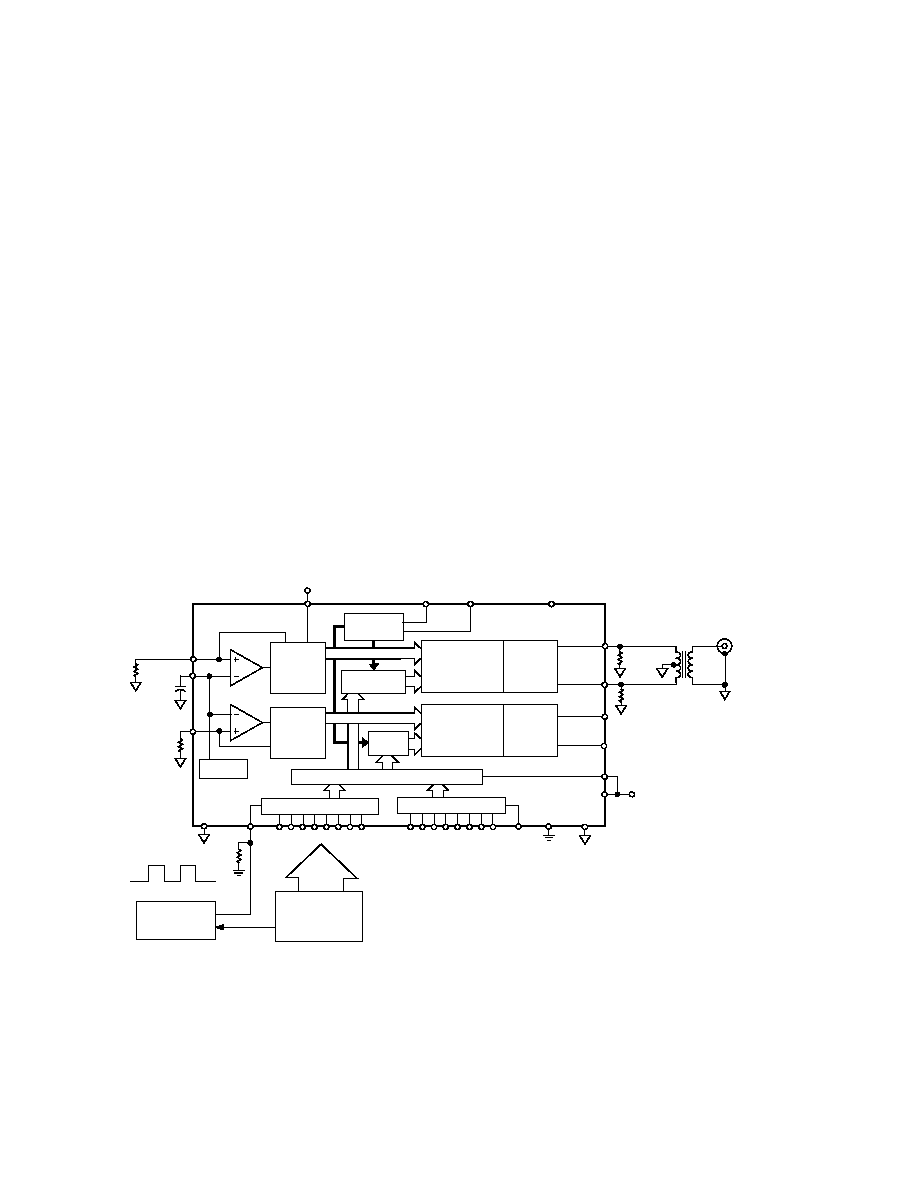
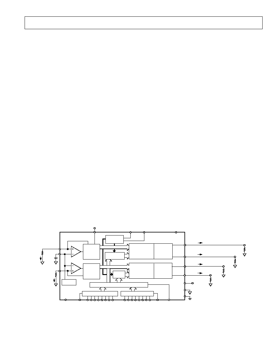
FUNCTIONAL DESCRIPTION
Figure 20 shows a simplified block diagram of the AD9709.
The AD9709 consists of two DACs, each one with its own
independent digital control logic and full-scale output current
control. Each DAC contains a PMOS current source array
capable of providing up to 20 mA of full-scale current (I
OUTFS
).
The array is divided into 31 equal currents that make up the five
most significant bits (MSBs). The three lower bits consist of
seven equal current sources whose value is 1/8th of an MSB
current source. Implementing the lower bits with current sources,
instead of an R-2R ladder, enhances the dynamic performance
for multitone or low-amplitude signals and helps maintain the
DACs high-output impedance (i.e., >100 k
).
All of these current sources are switched to one or the other of
the two output nodes (i.e., I
OUTA
or I
OUTB
) via PMOS differ-
ential current switches. The switches are based on a new archi-
tecture that drastically improves distortion performance. This
new switch architecture reduces various timing errors and pro-
vides matching complementary drive signals to the inputs of the
differential current switches.
The analog and digital sections of the AD9709 have separate
power supply inputs (i.e., AVDD and DVDD) that can operate
independently over a 3 V to 5.5 V range. The digital section,
which is capable of operating up to a 125 MSPS clock rate,
consists of edge-triggered latches and segment decoding logic
circuitry. The analog section includes the PMOS current sources,
the associated differential switches, a 1.20 V bandgap voltage
reference and two reference control amplifiers.
The full-scale output current of each DAC is regulated by sepa-
rate reference control amplifiers and can be set from 2 mA to
20 mA via an external resistor, R
SET
, connected to the Full-Scale
Adjust (FSADJ) pin. The external resistor, in combination with
both the reference control amplifier and voltage reference V
REFIO
,
sets the reference current I
REF
, which is replicated to the seg-
mented current sources with the proper scaling factor. The full-
scale current, I
OUTFS
, is 32
× I
REF
.
REFERENCE OPERATION
The AD9709 contains an internal 1.20 V bandgap reference.
This can be easily overridden by an external reference with no
effect on performance. REFIO serves as either an input or output
depending on whether the internal or an external reference is
used. To use the internal reference, simply decouple the REFIO
pin to ACOM with a 0.1
µF capacitor. The internal reference
voltage will be present at REFIO. If the voltage at REFIO is to
be used elsewhere in the circuit, an external buffer amplifier
with an input bias current of less than 100 nA should be used.
An example of the use of the internal reference is shown in
Figure 21.
An external reference can be applied to REFIO as shown in
Figure 22. The external reference may provide either a fixed
reference voltage to enhance accuracy and drift performance or
a varying reference voltage for gain control. Note that the 0.1
µF
compensation capacitor is not required since the internal refer-
ence is overridden, and the relatively high-input impedance of
REFIO minimizes any loading of the external reference.
GAINCTRL MODE
The AD9709 allows the gain of each channel to be set indepen-
dently by connecting one R
SET
resistor to FSADJ1 and another
R
SET
resistor to FSADJ2. To add flexibility and reduce system
cost, a single R
SET
resistor can be used to set the gain of both
channels simultaneously.
When GAINCTRL is low (i.e., connected to AGND), the inde-
pendent channel gain control mode using two resistors is enabled.
In this mode, individual R
SET
resistors should be connected to
FSADJ1 and FSADJ2. When GAINCTRL is high (i.e., connected
to AVDD), the master/slave channel gain control mode using one
resistor is enabled. In this mode, a single RSET resistor is con-
nected to FSADJ1 and the resistor on FSADJ2 can be removed.
DIGITAL DATA INPUTS
I
REF1
I
REF2
AVDD
DB0-DB7
GAINCTRL
WRT1/
IQWRT
1.2V REF
R
SET
2
2k
CHANNEL 1 LATCH
CHANNEL 2 LATCH
PMOS
CURRENT
SOURCE
ARRAY
PMOS
CURRENT
SOURCE
ARRAY
SEGMENTED
SWITCHES
FOR DAC1
SEGMENTED
SWITCHES
FOR DAC2
LSB
SWITCH
LSB
SWITCH
MULTIPLEXING LOGIC
AD9709
DCOM
MODE
SLEEP
CLK2/
IQRESET
CLK1/
IQCLK
5V
FSADJ1
R
SET
1
2k
REFIO
0.1 F
FSADJ2
DB0-DB7
WRT2/
IQSEL
5V
DVDD
DAC2
LATCH
DAC1
LATCH
CLK
DIVIDER
ACOM
I
OUTA1
I
OUTB1
R
L
1A
50
V
OUT
1A
R
L
1B
50
V
OUT
1B
R
L
2A
50
V
OUT
2A
R
L
2B
50
V
OUT
2B
I
OUTA2
I
OUTB2
V
DIFF
= V
OUT
A V
OUT
B
Figure 20. Simplified Block Diagram
REV. 0
AD9709
10
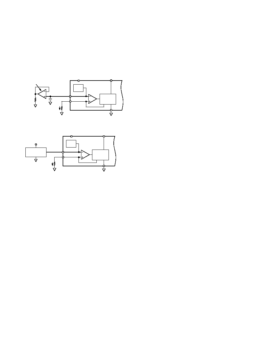
REFERENCE CONTROL AMPLIFIER
Both of the DACs in the AD9709 contain a control amplifier
that is used to regulate the full-scale output current, I
OUTFS
. The
control amplifier is configured as a V-I converter as shown in
Figure 21, so that its current output, I
REF
, is determined by the
ratio of the V
REFIO
and an external resistor, R
SET
, as stated in
Equation 4. I
REF
is copied to the segmented current sources with
the proper scale factor to set I
OUTFS
as stated in Equation 3.
+1.2V
REF
AVDD
GAINCTRL
CURRENT
SOURCE
ARRAY
REFIO
FSADJ
2k
0.1 F
ADDITIONAL
EXTERNAL
LOAD
OPTIONAL
EXTERNAL
REFERENCE
BUFFER
AD9709
REFERENCE
SECTION
I
REF
ACOM
Figure 21. Internal Reference Configuration
+1.2V
REF
AVDD
GAINCTRL
CURRENT
SOURCE
ARRAY
REFIO
FSADJ
2k
AD9709
REFERENCE
SECTION
I
REF
ACOM
AVDD
EXTERNAL
REFERENCE
Figure 22. External Reference Configuration
The control amplifier allows a wide (10:1) adjustment span of
I
OUTFS
from 2 mA to 20 mA by setting I
REF
between 62.5
µA
and 625
µA. The wide adjustment range of I
OUTFS
provides
several benefits. The first relates directly to the power dissipa-
tion of the AD9709, which is proportional to I
OUTFS
(refer to the
Power Dissipation section). The second relates to the 20 dB
adjustment, which is useful for system gain control purposes.
The small signal bandwidth of the reference control amplifier
is approximately 500 kHz and can be used for low frequency,
small signal multiplying applications.
DAC TRANSFER FUNCTION
Both DACs in the AD9709 provide complementary current out-
puts, I
OUTA
and I
OUTB
. I
OUTA
will provide a near full-scale current
output, I
OUTFS
, when all bits are high (i.e., DAC CODE = 1023)
while I
OUTB
, the complementary output, provides no current. The
current output appearing at I
OUTA
and I
OUTB
is a function of both
the input code and I
OUTFS
and can be expressed as:
I
OUTA
= (DAC CODE/256)
× I
OUTFS
(1)
I
OUTB
= (255 DAC CODE)/256
× I
OUTFS
(2)
where DAC CODE = 0 to 255 (i.e., Decimal Representation).
As mentioned previously, I
OUTFS
is a function of the reference
current I
REF
, which is nominally set by a reference voltage, V
REFIO
and external resistor R
SET
. It can be expressed as:
I
OUTFS
= 32
× I
REF
(3)
where
I
REF
= V
REFIO
/R
SET
(4)
The two current outputs will typically drive a resistive load
directly or via a transformer. If dc coupling is required, I
OUTA
and I
OUTB
should be directly connected to matching resistive
loads, R
LOAD
, that are tied to analog common, ACOM. Note,
R
LOAD
may represent the equivalent load resistance seen by
I
OUTA
or I
OUTB
as would be the case in a doubly terminated 50
or 75
cable. The single-ended voltage output appearing at the
I
OUTA
and I
OUTB
nodes is simply :
V
OUTA
= I
OUTA
× R
LOAD
(5)
V
OUTB
= I
OUTB
× R
LOAD
(6)
Note the full-scale value of V
OUTA
and V
OUTB
should not exceed
the specified output compliance range to maintain specified
distortion and linearity performance.
V
DIFF
= (I
OUTA
I
OUTB
)
× R
LOAD
(7)
Substituting the values of I
OUTA
, I
OUTB
and I
REF
; V
DIFF
can be
expressed as:
V
DIFF
= {(2
× DAC CODE 255)/256} ×
(32
× R
LOAD
/R
SET
)
× V
REFIO
(8)
These last two equations highlight some of the advantages of
operating the AD9709 differentially. First, the differential
operation will help cancel common-mode error sources associ-
ated with I
OUTA
and I
OUTB
such as noise, distortion and dc
offsets. Second, the differential code dependent current and
subsequent voltage, V
DIFF
, is twice the value of the single-ended
voltage output (i.e., V
OUTA
or V
OUTB
), thus providing twice the
signal power to the load.
Note, the gain drift temperature performance for a single-ended
(V
OUTA
and V
OUTB
) or differential output (V
DIFF
) of the AD9709
can be enhanced by selecting temperature tracking resistors for
R
LOAD
and R
SET
due to their ratiometric relationship as shown
in Equation 8.
ANALOG OUTPUTS
The complementary current outputs in each DAC, I
OUTA
and
I
OUTB
, may be configured for single-ended or differential opera-
tion. I
OUTA
and I
OUTB
can be converted into complementary
single-ended voltage outputs, V
OUTA
and V
OUTB
, via a load
resistor, R
LOAD
, as described in the DAC Transfer Function
section by Equations 5 through 8. The differential voltage, V
DIFF
,
existing between V
OUTA
and V
OUTB
can also be converted to a
single-ended voltage via a transformer or differential amplifier
configuration. The ac performance of the AD9709 is optimum
and specified using a differential transformer coupled output in
which the voltage swing at I
OUTA
and I
OUTB
is limited to
±0.5 V.
If a single-ended unipolar output is desirable, I
OUTA
should be
selected.
The distortion and noise performance of the AD9709 can be
enhanced when it is configured for differential operation. The
common-mode error sources of both I
OUTA
and I
OUTB
can be
significantly reduced by the common-mode rejection of a
transformer or differential amplifier. These common-mode error
sources include even-order distortion products and noise. The
enhancement in distortion performance becomes more signifi-
cant as the frequency content of the reconstructed waveform
increases. This is due to the first order cancellation of various
dynamic common-mode distortion mechanisms, digital feed-
through and noise.
REV. 0
AD9709
11
Performing a differential-to-single-ended conversion via a trans-
former also provides the ability to deliver twice the reconstructed
signal power to the load (i.e., assuming no source termination).
Since the output currents of I
OUTA
and I
OUTB
are complementary,
they become additive when processed differentially. A prop-
erly selected transformer will allow the AD9709 to provide the
required power and voltage levels to different loads.
The output impedance of I
OUTA
and I
OUTB
is determined by the
equivalent parallel combination of the PMOS switches associ-
ated with the current sources and is typically 100 k
in parallel
with 5 pF. It is also slightly dependent on the output voltage
(i.e., V
OUTA
and V
OUTB
) due to the nature of a PMOS device.
As a result, maintaining I
OUTA
and/or I
OUTB
at a virtual ground
via an I-V op amp configuration will result in the optimum dc
linearity. Note the INL/DNL specifications for the AD9709 are
measured with I
OUTA
maintained at a virtual ground via an op amp.
I
OUTA
and I
OUTB
also have a negative and positive voltage com-
pliance range that must be adhered to in order to achieve opti-
mum performance. The negative output compliance range of
1.0 V is set by the breakdown limits of the CMOS process.
Operation beyond this maximum limit may result in a break-
down of the output stage and affect the reliability of the AD9709.
The positive output compliance range is slightly dependent on
the full-scale output current, I
OUTFS
. It degrades slightly from its
nominal 1.25 V for an I
OUTFS
= 20 mA to 1.00 V for an I
OUTFS
=
2 mA. The optimum distortion performance for a single-ended
or differential output is achieved when the maximum full-scale
signal at I
OUTA
and I
OUTB
does not exceed 0.5 V. Applications
requiring the AD9709's output (i.e., V
OUTA
and/or V
OUTB
) to
extend its output compliance range should size R
LOAD
accord-
ingly. Operation beyond this compliance range will adversely
affect the AD9709's linearity performance and subsequently
degrade its distortion performance.
DIGITAL INPUTS
The AD9709's digital inputs consists of two independent chan-
nels. For the dual port mode, each DAC has its own dedicated
8-bit data port, WRT line and CLK line. In the interleaved
timing mode, the function of the digital control pins changes
as described below under the Interleaved Mode Timing section.
The 8-bit parallel data inputs follow straight binary coding
where DB7 is the most significant bit (MSB) and DB0 is the
least significant bit (LSB). I
OUTA
produces a full-scale output
current when all data bits are at Logic 1. I
OUTB
produces a
complementary output with the full-scale current split between
the two outputs as a function of the input code.
The digital interface is implemented using an edge-triggered
master slave latch. The DAC outputs are updated following
either the rising edge, or every other rising edge of the clock,
depending on whether dual or interleaved mode is being used.
The DAC outputs are designed to support a clock rate as high
as 125 MSPS. The clock can be operated at any duty cycle that
meets the specified latch pulsewidth. The setup and hold times
can also be varied within the clock cycle as long as the specified
minimum times are met, although the location of these transition
edges may affect digital feedthrough and distortion perfor-
mance. Best performance is typically achieved when the input
data transitions on the falling edge of a 50% duty cycle clock.
DAC TIMING
The AD9709 can operate in two timing modes, dual and inter-
leaved, which are described below. The block diagram in Figure
25 represents the latch architecture in the interleaved timing mode.
DUAL PORT MODE TIMING
When the mode pin is at Logic 1, the AD9709 operates in dual
port mode. The AD9709 functions as two distinct DACs. Each
DAC has its own completely independent digital input and con-
trol lines.
The AD9709 features a double buffered data path. Data enters
the device through the channel input latches. This data is then
transferred to the DAC latch in each signal path. Once the data
is loaded into the DAC latch, the analog output will settle to its
new value.
For general consideration, the WRT lines control the channel
input latches and the CLK lines control the DAC latches. Both
sets of latches are updated on the rising edge of their respective
control signals.
The rising edge of CLK should occur before or simultaneously
with the rising edge of WRT. Should the rising edge of CLK
occur after the rising edge of WRT, a 2 ns minimum delay should
be maintained from rising edge of WRT to rising edge of CLK.
WRT1/WRT2
CLK1/CLK2
DATA IN
IOUTA
OR
IOUTB
t
LPW
t
PD
t
S
t
H
t
CPW
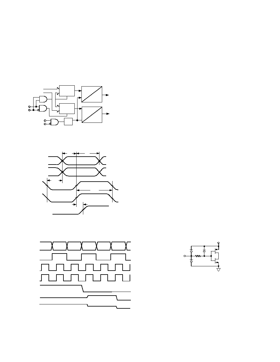
Figure 23. Dual Mode Timing
Timing specifications for dual port mode are given in Figures 23
and 24.
D1
D2
D3
D4
D5
DATAIN
WRT1/WRT2
CLK1/CLK2
xx
D1
D2
D3
D4
IOUTA
OR
IOUTB
Figure 24. Dual Mode Timing
INTERLEAVED MODE TIMING
When the mode pin is at Logic 0, the AD9709 operates in inter-
leaved mode. WRT1 now functions as IQWRT and CLK1
functions as IQCLK. WRT2 functions as IQSEL and CLK2
functions as IQRESET.
Data enters the device on the rising edge of IQWRT. The logic
level of IQSEL will steer the data to either Channel Latch 1
(IQSEL = 1) or to Channel Latch 2 (IQSEL = 0). Note: For
proper operation, IQSEL should only change state when IQWRT
and IQCLK are low.
REV. 0
AD9709
12
When IQRESET is high, IQCLK is disabled. When IQRESET
goes low, the following rising edge on IQCLK will update both
DAC latches with the data present at their inputs. In the inter-
leaved mode IQCLK is divided by 2 internally. Following this
first rising edge, the DAC latches will only be updated on every
other rising edge of IQCLK. In this way, IQRESET can be used
to synchronize the routing of the data to the DACs.
As with the dual port mode, IQCLK should occur before or
simultaneously with IQWRT.
IQSEL
IQWRT
DAC1
LATCH
DAC1
INTERLEAVED
DATA IN, PORT 1
DEINTERLEAVED
DATA OUT
IQCLK
IQRESET
DAC2
LATCH
DAC2
2
PORT 1
INPUT
LATCH
PORT 2
INPUT
LATCH
Figure 25. Latch Structure in Interleaved Mode
Timing specifications for interleaved mode are given in Figures
26 and 27.
DATA IN
IQWRT
IQCLK
IOUTA
OR
IOUTB
t
LPW
t
PD
t
S
t
H
t
H
*
IQSEL
*APPLIES TO FALLING EDGE OF IQCLK /IQWRT AND IQSEL ONLY
Figure 26. Interleaved Mode Timing
D1
D2
D3
D4
D5
INTERLEAVED
DATA
xx
xx
D1
D2
D3
D4
xx
IQSEL
IQWRT
IQRESET
DAC OUTPUT
PORT 1
DAC OUTPUT
PORT 2
IQCLK
Figure 27. Interleaved Mode Timing
The digital inputs are CMOS-compatible with logic thresholds,
V
THRESHOLD
, set to approximately half the digital positive supply
(DVDD) or
V
THRESHOLD
= DVDD/2 (
±20%)
The internal digital circuitry of the AD9709 is capable of oper-
ating over a digital supply range of 3 V to 5.5 V. As a result, the
digital inputs can also accommodate TTL levels when DVDD is
set to accommodate the maximum high-level voltage of the
TTL drivers V
OH
(MAX). A DVDD of 3 V to 3.3 V will typically
ensure proper compatibility with most TTL logic families. Fig-
ure 28 shows the equivalent digital input circuit for the data and
clock inputs. The sleep mode input is similar with the exception
that it contains an active pull-down circuit, thus ensuring that
the AD9709 remains enabled if this input is left disconnected.
Since the AD9709 is capable of being clocked up to 125 MSPS,
the quality of the clock and data input signals are important in
achieving the optimum performance. Operating the AD9709
with reduced logic swings and a corresponding digital supply
(DVDD) will result in the lowest data feedthrough and on-chip
digital noise. The drivers of the digital data interface circuitry
should be specified to meet the minimum setup and hold times
of the AD9709 as well as its required min/max input logic level
thresholds.
Digital signal paths should be kept short and run lengths matched
to avoid propagation delay mismatch. The insertion of a low-
value resistor network (i.e., 20
to 100 ) between the AD9709
digital inputs and driver outputs may be helpful in reducing any
overshooting and ringing at the digital inputs that contribute to
digital feedthrough. For longer board traces and high-data update
rates, stripline techniques with proper impedance and termina-
tion resistors should be considered to maintain "clean" digital
inputs.
The external clock driver circuitry should provide the AD9709
with a low-jitter clock input meeting the min/max logic levels
while providing fast edges. Fast clock edges will help minimize
any jitter that will manifest itself as phase noise on a reconstructed
waveform. Thus, the clock input should be driven by the fastest
logic family suitable for the application.
DVDD
DIGITAL
INPUT
Figure 28. Equivalent Digital Input
Note that the clock input could also be driven via a sine wave,
which is centered around the digital threshold (i.e., DVDD/2)
and meets the min/max logic threshold. This will typically result
in a slight degradation in the phase noise, which becomes more
noticeable at higher sampling rates and output frequencies.
Also, at higher sampling rates, the 20% tolerance of the digital
logic threshold should be considered since it will affect the
effective clock duty cycle and, subsequently, cut into the required
data setup and hold times.
REV. 0
AD9709
13
TIME OF DATA CHANGE RELATIVE TO
RISING CLOCK EDGE ns
SINAD
dBc
0
4
2
0
2
3
3
1
4
1
10
20
30
40
50
60
Figure 29. SINAD vs. Clock Placement @ f
OUT
= 20 MHz
INPUT CLOCK AND DATA TIMING RELATIONSHIP
SNR in a DAC is dependent on the relationship between the
position of the clock edges and the point in time at which the
input data changes. The AD9709 is rising edge triggered, and so
exhibits SNR sensitivity when the data transition is close to this
edge. In general, the goal when applying the AD9709 is to make
the data transition close to the falling clock edge. This becomes
more important as the sample rate increases. Figure 29 shows
the relationship of SNR to clock/data placement.
SLEEP MODE OPERATION
The AD9709 has a power down function that turns off the
output current and reduces the supply current to less than
8.5 mA over the specified supply range of 3.0 V to 5.5 V and
temperature range. This mode can be activated by applying a
logic level 1 to the SLEEP pin. The SLEEP pin logic threshold
is equal to 0.5
× AVDD. This digital input also contains an
active pull-down circuit that ensures the AD9709 remains
enabled if this input is left disconnected. The AD9709 takes
less than 50 ns to power down and approximately 5
µs to
power back up.
POWER DISSIPATION
The power dissipation, P
D
, of the AD9709 is dependent on
several factors that include: (1) The power supply voltages
(AVDD and DVDD), (2) the full-scale current output I
OUTFS
,
(3) the update rate f
CLOCK
, (4) and the reconstructed digital
input waveform. The power dissipation is directly proportional
to the analog supply current, I
AVDD
, and the digital supply cur-
rent, I
DVDD
. I
AVDD
is directly proportional to I
OUTFS
as shown in
Figure 30 and is insensitive to f
CLOCK
.
Conversely, I
DVDD
is dependent on both the digital input wave-
form, f
CLOCK
, and digital supply DVDD. Figures 31 and 32
show I
DVDD
as a function of full-scale sine wave output ratios
(f
OUT
/f
CLOCK
) for various update rates with DVDD = 5 V and
DVDD = 3 V, respectively. Note how I
DVDD
is reduced by more
than a factor of 2 when DVDD is reduced from 5 V to 3 V.
APPLYING THE AD9709
Output Configurations
The following sections illustrate some typical output configura-
tions for the AD9709. Unless otherwise noted, it is assumed
that I
OUTFS
is set to a nominal 20 mA. For applications requiring
the optimum dynamic performance, a differential output
configuration is suggested. A differential output configuration
may consist of either an RF transformer or a differential op amp
configuration. The transformer configuration provides the opti-
mum high-frequency performance and is recommended for any
application allowing for ac coupling. The differential op amp
configuration is suitable for applications requiring dc coupling,
a bipolar output, signal gain and/or level shifting, within the
bandwidth of the chosen op amp.
I
OUTFS
mA
0
5
10
10
I
AVDD
mA
20
30
40
50
60
70
80
15
20
25
Figure 30. I
AVDD
vs. I
OUTFS
RATIO f
OUT
/f
CLK
0
0.1
0
I
DVDD
mA
5
10
15
20
25
30
35
0.2
0.3
0.4
0.5
125MSPS
100MSPS
65MSPS
25MSPS
5MSPS
Figure 31. I
DVDD
vs. Ratio @ DVDD = 5 V
RATIO f
OUT
/f
CLK
0
0.1
0
I
DVDD
mA
2
4
6
8
10
12
14
0.2
0.3
0.4
0.5
16
18
125MSPS
100MSPS
65MSPS
25MSPS
5MSPS
Figure 32. I
DVDD
vs. Ratio @ DVDD = 3 V
REV. 0
AD9709
14
A single-ended output is suitable for applications requiring a
unipolar voltage output. A positive unipolar output voltage will
result if I
OUTA
and/or I
OUTB
is connected to an appropriately
sized load resistor, R
LOAD
, referred to ACOM. This configuration
may be more suitable for a single-supply system requiring a dc-
coupled, ground referred output voltage. Alternatively, an
amplifier could be configured as an I-V converter, thus converting
I
OUTA
or I
OUTB
into a negative unipolar voltage. This configuration
provides the best dc linearity since I
OUTA
or I
OUTB
is maintained at
a virtual ground. Note that I
OUTA
provides slightly better perfor-
mance than I
OUTB
.
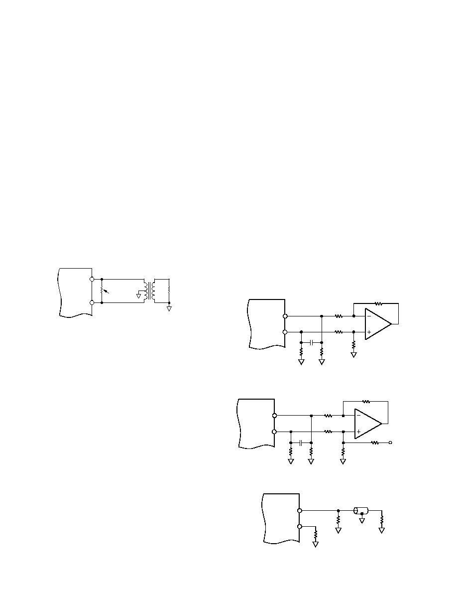
DIFFERENTIAL COUPLING USING A TRANSFORMER
An RF transformer can be used to perform a differential-to-
single-ended signal conversion as shown in Figure 33. A
differentially coupled transformer output provides the optimum
distortion performance for output signals whose spectral content
lies within the transformer's passband. An RF transformer such
as the Mini-Circuits T1-1T provides excellent rejection of
common-mode distortion (i.e., even-order harmonics) and
noise over a wide frequency range. It also provides electrical
isolation and the ability to deliver twice the power to the load.
Transformers with different impedance ratios may also be used
for impedance matching purposes. Note that the transformer
provides ac coupling only.
R
LOAD
AD9709
MINI-CIRCUITS
T1-1T
OPTIONAL
R
DIFF
I
OUTA
I
OUTB
Figure 33. Differential Output Using a Transformer
The center tap on the primary side of the transformer must be
connected to ACOM to provide the necessary dc current path
for both I
OUTA
and I
OUTB
. The complementary voltages appearing
at I
OUTA
and I
OUTB
(i.e., V
OUTA
and V
OUTB
) swing symmetrically
around ACOM and should be maintained with the specified
output compliance range of the AD9709. A differential resistor,
R
DIFF
, may be inserted in applications where the output of the
transformer is connected to the load, R
LOAD
, via a passive
reconstruction filter or cable. R
DIFF
is determined by the
transformer's impedance ratio and provides the proper source
termination that results in a low VSWR. Note that approximately
half the signal power will be dissipated across R
DIFF
.
DIFFERENTIAL COUPLING USING AN OP AMP
An op amp can also be used to perform a differential to single-
ended conversion as shown in Figure 34. The AD9709 is
configured with two equal load resistors, R
LOAD
, of 25
. The
differential voltage developed across I
OUTA
and I
OUTB
is converted
to a single-ended signal via the differential op amp configuration.
An optional capacitor can be installed across I
OUTA
and I
OUTB
,
forming a real pole in a low-pass filter. The addition of this
capacitor also enhances the op amps distortion performance by
preventing the DACs high-slewing output from overloading the
op amp's input.
The common-mode rejection of this configuration is typically
determined by the resistor matching. In this circuit, the differen-
tial op amp circuit using the AD8047 is configured to provide
some additional signal gain. The op amp must operate off of a
dual supply since its output is approximately
±1.0 V. A high-
speed amplifier capable of preserving the differential performance
of the AD9709 while meeting other system level objectives (i.e.,
cost, power) should be selected. The op amp's differential gain,
its gain setting resistor values, and full-scale output swing capa-
bilities should all be considered when optimizing this circuit.
The differential circuit shown in Figure 35 provides the necessary
level-shifting required in a single supply system. In this case,
AVDD which is the positive analog supply for both the AD9709
and the op amp is also used to level-shift the differential output
of the AD9709 to midsupply (i.e., AVDD/2). The AD8041 is a
suitable op amp for this application.
SINGLE-ENDED UNBUFFERED VOLTAGE OUTPUT
Figure 36 shows the AD9709 configured to provide a unipolar
output range of approximately 0 V to 0.5 V for a doubly termi-
nated 50
cable since the nominal full-scale current, I
OUTFS
, of
20 mA flows through the equivalent R
LOAD
of 25
. In this case,
R
LOAD
represents the equivalent load resistance seen by I
OUTA
or
I
OUTB
. The unused output (I
OUTA
or I
OUTB
) can be connected to
ACOM directly or via a matching R
LOAD
. Different values of
I
OUTFS
and R
LOAD
can be selected as long as the positive compli-
ance range is adhered to. One additional consideration in this
mode is the integral nonlinearity (INL) as discussed in the
Analog Output section of this data sheet. For optimum INL
performance, the single-ended, buffered voltage output configu-
ration is suggested.
AD9709
500
225
225
500
25
25
AD8047
C
OPT
I
OUTA
I
OUTB
Figure 34. DC Differential Coupling Using an Op Amp
AD9709
I
OUTA
I
OUTB
C
OPT
500
225
225
500
25
25
AD8041
1k
AVDD
Figure 35. Single Supply DC Differential Coupled Circuit
AD9709
50
I
OUTA
I
OUTB
Figure 36. 0 V to 0.5 V Unbuffered Voltage Output
REV. 0
AD9709
15
SINGLE-ENDED, BUFFERED VOLTAGE OUTPUT
CONFIGURATION
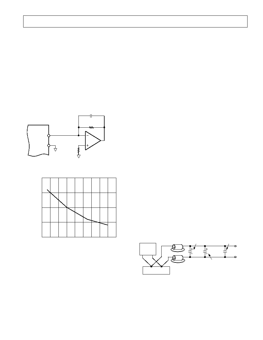
Figure 37 shows a buffered single-ended output configuration
in which the op amp U1 performs an I-V conversion on the
AD9709 output current. U1 maintains I
OUTA
(or I
OUTB
) at a
virtual ground, thus minimizing the nonlinear output imped-
ance effect on the DAC's INL performance as discussed in
the Analog Output section. Although this single-ended configu-
ration typically provides the best dc linearity performance, its ac
distortion performance at higher DAC update rates may be
limited by U1's slewing capabilities. U1 provides a negative
unipolar output voltage and its full-scale output voltage is simply
the product of R
FB
and I
OUTFS
. The full-scale output should be
set within U1's voltage output swing capabilities by scaling I
OUTFS
and/or R
FB
. An improvement in ac distortion performance may
result with a reduced I
OUTFS
since the signal current U1 will be
required to sink will be subsequently reduced.
I
OUTA
I
OUTB
AD9709
200
U1
V
OUT
= I
OUTFS
R
FB
R
FB
200
Figure 37. Unipolar Buffered Voltage Output
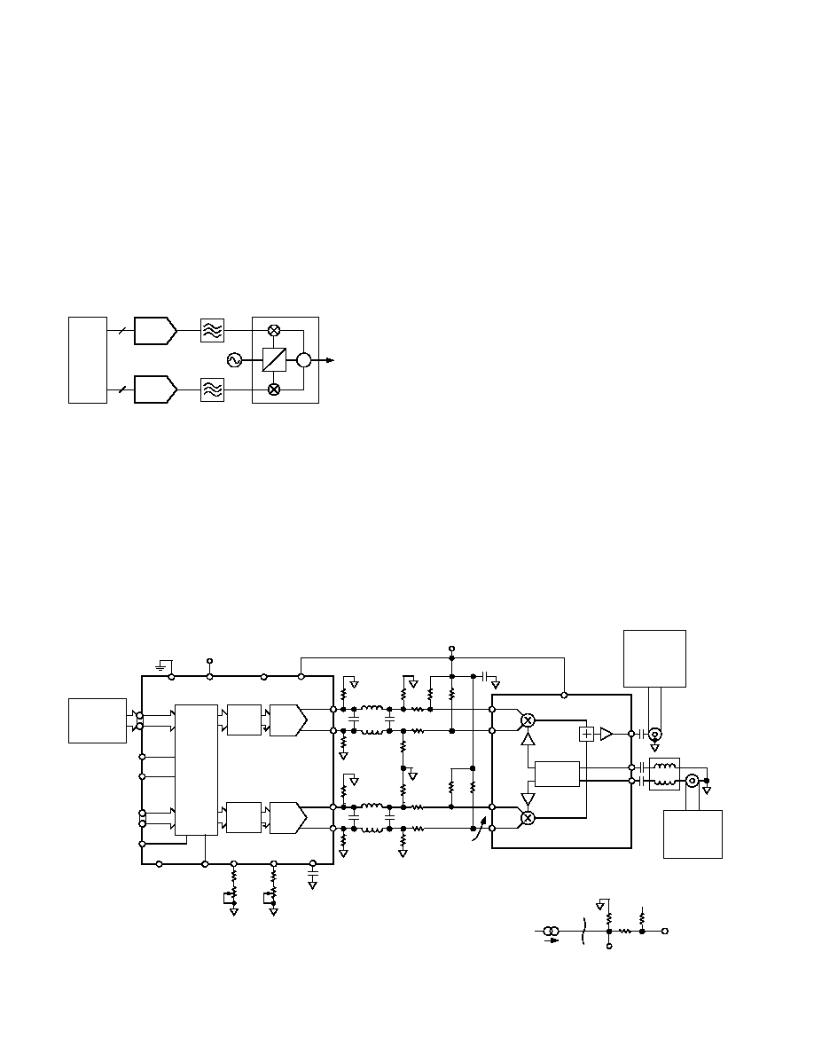
FREQUENCY MHz
PSRR
dB
90
70
0.2
85
80
75
0.3
0.4
0.5
0.6
0.7
0.8
0.9
1.0
1.1
Figure 38. AVDD Power Supply Rejection Ratio
POWER AND GROUNDING CONSIDERATIONS, POWER
SUPPLY REJECTION
Many applications seek high-speed and high-performance
under less than ideal operating conditions. In these application
circuits, the implementation and construction of the printed
circuit board is as important as the circuit design. Proper RF
techniques must be used for device selection, placement and
routing as well as power supply bypassing and grounding to
ensure optimum performance.
One factor that can measurably affect system performance is the
ability of the DAC output to reject dc variations or ac noise
superimposed on the analog or digital dc power distribution.
This is referred to as the Power Supply Rejection Ratio. For dc
variations of the power supply, the resulting performance of the
DAC directly corresponds to a gain error associated with the
DAC's full-scale current, I
OUTFS
. AC noise on the DC supplies
is common in applications where the power distribution is gen-
erated by a switching power supply. Typically, switching power
supply noise will occur over the spectrum from tens of kHz to
several MHz. The PSRR vs. frequency of the AD9709 AVDD
supply over this frequency range is shown in Figure 38.
Note that the units in Figure 38 are given in units of (amps out/
volts in). Noise on the analog power supply has the effect of
modulating the internal current sources, and therefore the
output current. The voltage noise on AVDD, therefore, will be
added in a nonlinear manner to the desired I
OUT
. PSRR is very
code dependent, thus producing mixing effects which can
modulate low-frequency power supply noise to higher frequen-
cies. Worst case PSRR for either one of the differential DAC
outputs will occur when the full-scale current is directed to-
wards that output. As a result, the PSRR measurement in Fig-
ure 38 represents a worst-case condition in which the digital
inputs remain static and the full-scale output current of 20 mA is
directed to the DAC output being measured.
An example serves to illustrate the effect of supply noise on the
analog supply. Suppose a switching regulator with a switching
frequency of 250 kHz produces 10 mV of noise and for simplic-
ity sake (i.e., ignore harmonics), all of this noise is concentrated
at 250 kHz. To calculate how much of this undesired noise will
appear as current noise superimposed on the dc's full-scale
current, I
OUTFS
, one must determine the PSRR in dB using
Figure 38 at 250 kHz. To calculate the PSRR for a given R
LOAD
,
such that the units of PSRR are converted from A/V to V/V,
adjust the curve in Figure 38 by the scaling factor 20
× Log
(R
LOAD
). For instance, if R
LOAD
is the PSRR is reduced by
34 dB (i.e., PSRR of the DAC at 250 kHz which is 85 dB in
Figure 38 becomes 51 dB V
OUT
/V
IN
).
Proper grounding and decoupling should be a primary objective
in any high-speed, high-resolution system. The AD9709 fea-
tures separate analog and digital supply and ground pins to
optimize the management of analog and digital ground currents
in a system. In general, AVDD, the analog supply, should be
decoupled to ACOM, the analog common, as close to the chip
as physically possible. Similarly, DVDD, the digital supply, should
be decoupled to DCOM as close to the chip as physically possible.
100 F
10 F22 F
0.1 F
TTL/CMOS
LOGIC
CIRCUITS
+5V
POWER SUPPLY
FERRITE
BEADS
AVDD
ACOM
ELECTROLYTIC
TANTALUM
CERAMIC
Figure 39. Differential LC Filter for Single 5 V and 3 V
Applications
For those applications that require a single 5 V or 3 V supply for
both the analog and digital supplies, a clean analog supply may
be generated using the circuit shown in Figure 39. The circuit
consists of a differential LC filter with separate power supply
and return lines. Lower noise can be attained by using low-ESR
type electrolytic and tantalum capacitors.
REV. 0
AD9709
16
APPLICATIONS
Using the AD9709 for Quadrature Amplitude Modulation
QAM is one of the most widely used digital modulation schemes
in digital communications systems. This modulation technique
can be found in FDM as well as spread spectrum (i.e., CDMA)
based systems. A QAM signal is a carrier frequency that is
modulated in both amplitude (i.e., AM modulation) and phase
(i.e., PM modulation). It can be generated by independently
modulating two carriers of identical frequency but with a 90
°
phase difference. This results in an in-phase (I) carrier compo-
nent and a quadrature (Q) carrier component at a 90
° phase
shift with respect to the I component. The I and Q components
are then summed to provide a QAM signal at the specified car-
rier frequency.
DAC
CARRIER
FREQUENCY
8
8
TO
MIXER
NYQUIST
FILTERS
QUADRATURE
MODULATOR
DAC
DSP
OR
ASIC
0
90
Figure 40. Typical Analog QAM Architecture
A common and traditional implementation of a QAM modula-
tor is shown in Figure 40. The modulation is performed in the
analog domain in which two DACs are used to generate the
baseband I and Q components. Each component is then typically
applied to a Nyquist filter before being applied to a quadrature
mixer. The matching Nyquist filters shape and limit each com-
ponents spectral envelope while minimizing intersymbol inter-
ference. The DAC is typically updated at the QAM symbol rate
or possibly a multiple of it if an interpolating filter precedes
the DAC. The use of an interpolating filter typically eases the
implementation and complexity of the analog filter, which can
be a significant contributor to mismatches in gain and phase
between the two baseband channels. A quadrature mixer modu-
lates the I and Q components with the in-phase and quadrature
carrier frequency and then sums the two outputs to provide the
QAM signal.
In this implementation, it is much more difficult to maintain
proper gain and phase matching between the I and Q channels.
The circuit implementation shown in Figure 41 helps improve
upon the matching between the I and Q channels, as well as
showing a path for up-conversion using the AD8346 quadrature
modulator. The AD9709 provides both I and Q DACs as well as
a common reference that will improve the gain matching and
stability. R
CAL
can be used to compensate for any mismatch in
gain between the two channels. The mismatch may be attributed
to the mismatch between R
SET1
and R
SET2
, effective load resis-
tance of each channel, and/or the voltage offset of the control
amplifier in each DAC. The differential voltage outputs of both
DACs in the AD9709 are fed into the respective differential
inputs of the AD8346 via matching networks.
I and Q digital data can be fed into the AD9709 in two different
ways. In dual port mode, The digital I information drives one
input port, while the digital Q information drives the other input
port. If no interpolation filter precedes the DAC, the symbol
rate will be the rate at which the system clock drives the CLK
and WRT pins on the AD9709. In interleaved mode, the digital
input stream at Port I contains the I and the Q information in
alternating digital words. Using IQSEL and IQRESET, the
AD9709 can be synchronized to the I and Q data stream. The
internal timing of the AD9709 routes the selected I and Q data
to the correct DAC output. In interleaved mode, if no inter-
polation filter precedes the AD9709, the symbol rate will be
half that of the system clock driving the digital datastream and
the IQWRT and IQCLK pins on the AD9709.
IOUTA
IOUTB
QOUTA
QOUTB
RB
RA
V
MOD
AVDD
RL
AD8346
AD976x
0 TO I
OUTFS
V
DAC
DCOM
FSADJI
REFIO
SLEEP
R
SET
3.9k
0.1 F
DVDD
AVDD
CA
0.1 F
VPBF
BBIP
BBIN
BBQP
BBQN
AD8346
LOIP
LOIN
VOUT
IQWRT
IQCLK
ACOM
AD9709
"I"
DAC
RL
LA
RL
CB
LA
RL
RB
RB
RL
RA
RA
AVDD
RL
CA
RL
LA
RL
CB
LA
RB
RB
RL
RA
RA
C
FILTER
DIFFERENTIAL
RLC FILTER
VDIFF = 1.82V p-p
"Q"
DAC
LATCH
PHASE
SPLITTER
ROHDE &
SCHWARZ
FSEA30B
SPECTRUM
ANALYZER
ROHDE &
SCHWARZ
SIGNAL
GENERATOR
PORT I
PORT Q
TEKTRONICS
AWG2021
W/OPTION 4
D
I
G
I
T
A
L
I
N
T
E
R
F
A
C
E
IQSEL
FSADJQ
R
SET
3.9k
MODE
CB = 45pF
LA = 10 H
I
OUTFS
= 11mA
AVDD = 5.0V
VCM = 1.2V
NOTE:
RL = 200
RA = 2500
RB = 500
RP = 200
CA = 280pF
"Q"
DAC
"I"
DAC
LATCH
NOTE: DACs Full-Scale OUTPUT CURRENT = I
OUTFS
RA, RB AND RL ARE THIN FILM RESISTOR NETWORKSWITH
0.1% MATCHING, 1% ACCURACY.
AVAILABLE FROM OHMTEK ORNXXXXD SERIES.
Figure 41. Baseband QAM Implementation Using an AD9709 and AD8346
REV. 0
AD9709
17
CDMA
Carrier Division Multiple Access, or CDMA, is an air transmit/
receive scheme where the signal in the transmit path is modulated
with a pseudorandom digital code (sometimes referred to as the
spreading code). The effect of this is to spread the transmitted
signal across a wide spectrum. Similar to a DMT waveform, a
CDMA waveform containing multiple subscribers can be char-
acterized as having a high peak to average ratio (i.e., crest factor),
thus demanding highly linear components in the transmit signal
path. The bandwidth of the spectrum is defined by the CDMA
standard being used, and in operation is implemented by using
a spreading code with particular characteristics.
Distortion in the transmit path can lead to power being trans-
mitted out of the defined band. The ratio of power transmitted
in-band to out-of-band is often referred to as Adjacent Channel
Power (ACP). This is a regulatory issue due to the possibility
of interference with other signals being transmitted by air.
Regulatory bodies define a spectral mask outside of the transmit
band, and the ACP must fall under this mask. If distortion in
the transmit path causes the ACP to be above the spectral mask,
then filtering, or different component selection is needed to
meet the mask requirements.
Figure 42 shows the AD9709/AD8346 application circuit of
Figure 41 reconstructing a wideband, or W-CDMA test vector
with a bandwith of 8 MHz, centered at 2.4 GHz and being
sampled at 62.5 MHz. The IF frequency at the DAC output
is 15.625 MHz. ACPR for the given test vector is measured
at greater than 54 dB.
FREQUENCY
CENTER 2.4GHz 3MHz SPAN 30MHz
cu1
c11
130
120
110
100
90
80
70
60
50
40
30
dBm
1
C2
cu1
C0
c11
Figure 42. CDMA Signal, 8 M Chips Sampled at 65 MSPS,
Recreated at 2.4 GHz, Adjacent Channel Power > 54 dBm
Figure 43 shows an example of the AD9709 used in a W-CDMA
transmitter application using the AD6122 CDMA 3 V IF sub-
system. The AD6122 has functions, such as external gain
control and low-distortion characteristics, needed for the
superior Adjacent Channel Power (ACP) requirements of
W-CDMA.
("Q DAC")
IOUTA
QOUTA
QOUTB
DCOM
FSADJ2
REFIO
SLEEP
R
SET2
1.9k
0.1 F
CLK2
Q DATA
INPUT
I DATA
INPUT
DVDD
AVDD
500
50
500
500
IIPP
IIPN
IIQP
IIQN
AD6122
CLK1
FSADJ1
R
SET1
2k
R
CAL
220
500
50
DAC
LATCH
DAC
("I DAC")
INPUT
LATCHES
WRT1
WRT2
ACOM
AD9709
U1
U2
LOIPP
LOIPN
2
PHASE
SPLITTER
REFIN
VGAIN
GAIN
CONTROL
TXOPP
TXOPN
GAIN
CONTROL
SCALE
FACTOR
TEMPERATURE
COMPENSATION
MODOPN
MODOPP
V
CC
V
CC
3V
500
500
IOUTB
INPUT
LATCHES
500
50
500
50
DAC
LATCH
DAC
634
Figure 43. CDMA Transmit Application Using AD9709 and AD6122
REV. 0
18
AD9709
EVALUATION BOARD
General Description
The AD9709-EB is an evaluation board for the AD9709 8-bit
dual D/A converter. Careful attention to layout and circuit
design, combined with a prototyping area, allow the user to
easily and effectively evaluate the AD9709 in any application
where high resolution, high speed conversion is required. This
board allows the user flexibility to operate the AD9709 in
various configurations. Possible output configurations include
transformer coupled, resistor terminated, and single and differ-
ential outputs. The digital inputs can be used in dual port or
interleaved mode, and are designed to be driven from various
word generators, with the on-board option to add a resistor
network for proper load termination. When operating the
AD9709, best performance is obtained when running the Digital
Supply (DVDD) at 3 V and the Analog Supply (AVDD) at 5 V.
WHT
TP29
WHT
TP30
WHT
TP31
WHT
TP32
DGND;3,4,5
DGND;3,4,5
DGND;3,4,5
DGND;3,4,5
S1
S2
S3
S4
WRT1IN
IQWRT
CLK1IN
IQCLK
CLK2IN
RESET
WRT2IN
IQSEL
1
2
R1
50
1
2
R2
50
1
2
R3
50
1
2
R4
50
1
2
3
JP5
JP16
1
2
3
A
B
JP4
1
2
3
A
B
JP3
2
3
5
6
4
1
DGND;8
DVDD;16
TSSOP112
1
2
3
A
B
JP7
JP2
JP1
DVDD
1
2
3
A
B
JP6
DVDD
/2 CLOCK DIVIDER
WRT1
CLK1
CLK2
WRT2
WHT
TP33
SLEEP
1
2
R13
50
SLEEP
J
CLK
Q
Q
PRE
CLR
U1
K
DVDD
15
I
C
I
C
A
B
I
C
1
2
3
A
B
JP9
DCLKIN1
DCLKIN2
14
12
11
9
7
10
13
DGND;8
DVDD;16
TSSOP112
J
CLK
Q
Q
PRE
CLR
U2
K
RED
TP10
B1
BAN-JACK
DVDDIN
L1
BEAD
1
2
C9
10 F
25V
BLK
TP37
BLK
TP38
TP43
BLK
BLK
TP39
DGND
DVDD
B2
BAN-JACK
RED
TP11
B3
BAN-JACK
AVDDIN
L2
BEAD
1
2
C10
10 F
25V
BLK
TP40
BLK
TP41
TP44
BLK
BLK
TP42
AGND
AVDD
B4
BAN-JACK
1
2
C7
0.1 F
1
2
C8
0.01 F
DVDD
POWER DECOUPLING AND INPUT CLOCKS
R1
22
INP1
2
1
RCOM
R2
22
INP2
3
R3
22
INP3
4
R4
22
INP4
5
R5
22
INP5
6
R6
22
INP6
7
R7
22
INP7
8
R8
22
INP8
9
R9
22
10
RP16
R1
22
INP9
2
1
RCOM
R2
22
INP10
3
R3
22
INP11
4
R4
22
INP12
5
R5
22
INP13
6
R6
22
INP14
7
R7
22
8
R8
22
INCK1
9
R9
22
10
RP9
R1
22
INP23
2
1
RCOM
R2
22
INP24
3
R3
22
INP25
4
R4
22
INP26
5
R5
22
INP27
6
R6
22
INP28
7
R7
22
INP29
8
R8
22
INP30
9
R9
22
10
RP10
R1
22
INP31
2
1
RCOM
R2
22
INP32
3
R3
22
INP33
4
R4
22
INP34
5
R5
22
INP35
6
R6
22
INP36
7
R7
22
8
R8
22
INCK2
9
R9
22
10
RP15
Figure 44. Power Decoupling and Clocks on AD9709 Evaluation Board
REV. 0
AD9709
19
RP11
10
9
8
7
6
5
4
3
2
1
R1
R9
RCOM
33
1
16
RP5, 10
3
14
RP5, 10
5
12
RP5, 10
7
10
RP5, 10
1
16
RP6, 10
3
14
RP6, 10
5
12
RP6, 10
2
15
13
11
9
15
13
11
DVDD
RP3
10
9
8
7
6
5
4
3
2
1
R1
R9
RCOM
22
RP5, 10
4
RP5, 10
6
RP5, 10
8
RP5, 10
2
RP6, 10
4
RP6, 10
6
RP6, 10
8
9
RP6, 10
DUTP1
DUTP2
DUTP3
DUTP4
DUTP5
DUTP6
DUTP7
DUTP8
DUTP9
DUTP10
DUTP11
DUTP12
DUTP13
DUTP14
DCLKIN1
DVDD
RP1
10
9
8
7
6
5
4
3
2
1
R1
R9
RCOM
22
RP13
10
9
8
7
6
5
4
3
2
1
R1
R9
RCOM
33
2 P1
P1 1
4 P1
P1 3
6 P1
P1 5
8 P1
P1 7
10
P1
P1 9
12 P1
P1 11
14 P1
P1 13
16 P1
P1 15
18 P1
P1 17
20 P1
P1 19
22 P1
P1 21
24 P1
P1 23
26 P1
P1 25
28 P1
P1 27
30 P1
P1 29
32 P1
P1 31
34 P1
P1 33
36 P1
P1 35
38 P1
P1 37
40 P1
P1 39
1
16
RP7, 10
3
14
RP7, 10
5
12
RP7, 10
7
10
RP7, 10
1
16
RP8, 10
3
14
RP8, 10
5
12
RP8, 10
2
15
13
11
9
15
13
11
RP7, 10
4
RP7, 10
6
RP7, 10
8
RP7, 10
2
RP8, 10
4
RP8, 10
6
RP8, 10
8
9
RP8, 10
DUTP23
DUTP24
DUTP25
DUTP26
DUTP27
DUTP28
DUTP29
DUTP30
DUTP31
DUTP32
DUTP33
DUTP34
DUTP35
DUTP36
DCLKIN2
7
10
RP5, 10
7
10
RP8, 10
SPARES
2 P2
P2 1
4 P2
P2 3
6 P2
P2 5
8 P2
P2 7
10
P2
P2 9
12 P2
P2 11
14 P2
P2 13
16 P2
P2 15
18 P2
P2 17
20 P2
P2 19
22 P2
P2 21
24 P2
P2 23
26 P2
P2 25
28 P2
P2 27
30 P2
P2 29
32 P2
P2 31
34 P2
P2 33
36 P2
P2 35
38 P2
P2 37
40 P2
P2 39
RP12
10
9
8
7
6
5
4
3
2
1
R1
R9
RCOM
33
DVDD
RP4
10
9
8
7
6
5
4
3
2
1
R1
R9
RCOM
22
DVDD
RP2
10
9
8
7
6
5
4
3
2
1
R1
R9
RCOM
22
RP14
10
9
8
7
6
5
4
3
2
1
R1
R9
RCOM
33
INP1
INP2
INP3
INP4
INP5
INP6
INP7
INP8
INP9
INP10
INP11
INP12
INP13
INP14
INCK1
INCK2
INP23
INP24
INP25
INP26
INP27
INP28
INP29
INP30
INP31
INP32
INP33
INP34
INP35
INP36
DIGITAL INPUT SIGNAL CONDITIONING
Figure 45. Digital Input Signal Conditioning
REV. 0
AD9709
20
WHT
TP46
1
2
R10
1.92k
1
2
3
4
5
6
7
8
9
10
11
12
13
14
15
16
17
18
19
20
21
22
23
24
48
47
46
45
44
43
42
41
40
39
38
37
36
35
34
33
32
31
30
29
28
27
26
25
DB13P1MSB
DB12P1
DB11P1
DB10P1
DB9P1
DB8P1
DB7P1
DB6P1
DB5P1
DB4P1
DB3P1
DB2P1
DB1P1
DB0P1
DCOM1
DVDD1
WRT1
CLK1
CLK2
WRT2
DCOM2
DVDD2
DB13P2MSB
DB12P2
MODE
AVDD
IA1
IB1
FSADJ1
REFIO
GAINCTRL
FSADJ2
IA2
IB2
ACOM
SLEEP
DB0P2
DB1P2
DB2P2
DB3P2
DB4P2
DB5P2
DB6P2
DB7P2
DB8P2
DB9P2
DB10P2
DB11P2
U2
1
2
C1
VAL
1
2
C2
0.01 F
1
2
C3
0.1 F
DVDD
1
2
3
A B
JP8
DVDD
1
2
C11
1 F
1
2
C12
0.01 F
1
2
C13
0.1 F
AVDD
SLEEP
DUTP36
DUTP35
DUTP34
DUTP33
DUTP32
DUTP31
DUTP30
DUTP29
DUTP28
DUTP27
DUTP26
DUTP25
1
2
C15
10pF
1
2
R7
50
1
2
C6
10pF
1
2
R8
50
WRT1
CLK1
CLK2
WRT2
DUTP23
DUTP24
DUTP1
DUTP2
DUTP3
DUTP4
DUTP5
DUTP6
DUTP7
DUTP8
DUTP9
DUTP10
DUTP11
DUTP12
DUTP13
DUTP14
1
2
C4
10pF
1
2
R5
50
1
2
C5
10pF
1
2
R6
50
TP34
WHT
R11
VAL
1:1
3
2
1
6
4
NC = 5
T1
AGND;3,4,5
S6
OUT1
TP45
WHT
1
2
R9
1.92k
TP36
WHT
REFIO
1
2
C14
0.1 F
DUT AND ANALOG OUTPUT SIGNAL CONDITIONING
1
2
3
A B
JP15
AVDD
MODE
ACOM
BL1
BL2
1
2
C16
22nF
1
2
R15
256
1
2
C17
22nF
1
2
R14
256
JP10
TP35
WHT
R12
VAL
1:1
3
2
1
6
4
NC = 5
T2
AGND;3,4,5
S11
OUT2
BL3
BL4
Figure 46. AD9709 and Output Signal Conditioning
REV. 0
AD9709
21
Figure 47. Assembly, Top Side
REV. 0
AD9709
22
Figure 48. Assembly, Bottom Side
REV. 0
AD9709
23
Figure 49. Layer 1, Top Side
REV. 0
AD9709
24
Figure 50. Layer 2, Ground Plane
REV. 0
AD9709
25
Figure 51. Layer 3, Power Plane
REV. 0
AD9709
26
Figure 52. Layer 4, Bottom Side
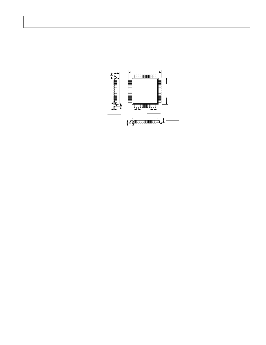
REV. 0
AD9709
27
48-Lead Thin Plastic Quad Flatpack (LQFP)
(ST-48)
TOP VIEW
(PINS DOWN)
1
12
13
25
24
36
37
48
0.019 (0.5)
BSC
0.276
(7.00)
BSC
SQ
0.011 (0.27)
0.006 (0.17)
0.354 (9.00) BSC SQ
0.063 (1.60)
MAX
0.030 (0.75)
0.018 (0.45)
0.008 (0.2)
0.004 (0.09)
0
MIN
COPLANARITY
0.003 (0.08)
SEATING
PLANE
0.006 (0.15)
0.002 (0.05)
7
0
0.057 (1.45)
0.053 (1.35)
OUTLINE DIMENSIONS
Dimensions shown in inches and (mm).
C370185/00 (rev. 0) 00606
PRINTED IN U.S.A.