 | –≠–ª–µ–∫—Ç—Ä–æ–Ω–Ω—ã–π –∫–æ–º–ø–æ–Ω–µ–Ω—Ç: AD9726 | –°–∫–∞—á–∞—Ç—å:  PDF PDF  ZIP ZIP |
Document Outline
- FEATURES
- APPLICATIONS
- GENERAL DESCRIPTION
- FUNCTIONAL BLOCK DIAGRAM
- PRODUCT HIGHLIGHTS
- ˛ˇ
- ˛ˇ
- ˛ˇ
- ˛ˇ
- ˛ˇ
- ˛ˇ
- ˛ˇ
- ˛ˇ
- ˛ˇ
- ˛ˇ
- ˛ˇ
- ˛ˇ
- ˛ˇ
- ˛ˇ
- ˛ˇ
- ˛ˇ
- ˛ˇ
- ˛ˇ
- ˛ˇ
- ˛ˇ
- ˛ˇ
- ˛ˇ
- ˛ˇ
- ˛ˇ
- ˛ˇ
- ˛ˇ
- ˛ˇ
- ˛ˇ

16-Bit, 400 MSPS
D/A Converter
AD9726
Rev. 0
Information furnished by Analog Devices is believed to be accurate and reliable.
However, no responsibility is assumed by Analog Devices for its use, nor for any
infringements of patents or other rights of third parties that may result from its
use. Specifications subject to change without notice. No license is granted by
implication or otherwise under any patent or patent rights of Analog Devices.
Trademarks and registered trademarks are the property of their respective owners.
One Technology Way, P.O. Box 9106, Norwood, MA 02062-9106, U.S.A.
Tel: 781.329.4700
www.analog.com
Fax: 781.461.3113
© 2005 Analog Devices, Inc. All rights reserved.
FEATURES
400 MSPS update rate
Dynamic performance
SFDR 78 dBc @ f
OUT
= 20 MHz
IMD 82 dBc @ f
OUT
= 70 MHz
ACLR 76 dBc @ f
OUT
= 70 MHz
NSD ≠160 dB/Hz @ f
OUT
= 70 MHz
Precision calibrated linearity
DNL ±0.5 LSB @ +25∞C
INL ±1.0 LSB @ +25∞C
THD ≠95 dB @ f
OUT
= 1 MHz
LVDS inputs with internal 100 terminations
Automatic data/clock timing synchronization
Single data rate or double data rate capable
Differential current outputs
Internal precision reference
Operates on 2.5 V and 3.3 V supplies
Extended industrial temperature range
Thermally enhanced, 80-lead, lead-free TQFP package
APPLICATIONS
Instrumentation
Test equipment
Waveform synthesis
Communication systems
FUNCTIONAL BLOCK DIAGRAM
INTERNAL
REFERENCE
CALIBRATION
MEMORY
LVDS OUTPUT
DRIVER
DATA S
Y
NCHRONIZATION
LV
DS
INP
U
T DATA CAP
TURE
SPI
CSB
SDIO
SDO
RESET
I
OUTA
I
OUTB
REFIO
FSADJ
SCLK
CLK+
CLK≠
DCLK_OUT+
DCLK_OUT≠
DB[15]+
DB[15]≠
DB[0]+
DB[0]≠
DCLK_IN+
DCLK_IN≠
CLOCK DISTRIBUTION
AND CONTROL
16-BIT
DAC
04540-001
Figure 1.
GENERAL DESCRIPTION
The AD9726 is a 16-bit digital-to-analog converter (DAC)
that offers leading edge performance at conversion rates up to
400 MSPS. The device uses low voltage differential signaling
(LVDS) inputs and includes internal 100 terminations. The
analog output can be single-ended or differential current. An
internal precision reference is included.
The AD9726 also features synchronization logic to monitor and
optimize the timing between incoming data and the sample
clock. This reduces system complexity and simplifies timing
requirements. An LVDS clock output is also available to drive
an external data pump in either single data rate (SDR) or double
data rate (DDR) mode.
All device operation is fully programmable using the flexible
serial port interface (SPI). The AD9726 is also fully functional
in its default state for applications without a controller.
PRODUCT HIGHLIGHTS
1.
A unique combination of precision and performance
makes the AD9726 equally suited to applications with
demanding frequency domain or demanding time domain
requirements.
2.
Nonvolatile factory calibration assures a highly linear
transfer function. Internal logic offers on demand self-
calibration for linearity even at extended operating
temperatures.
3.
Proprietary architecture minimizes data dependent,
discrete mixing spurs and offers enhanced dynamic
performance over a wide range of output frequencies.
High input data rates create a very high frequency
synthesis bandwidth.
4.
The fully automatic, transparent synchronizer maintains
optimized timing between clock and data in real time and
offers programmable control options for added flexibility.
5.
Full-scale output current is external resistor
programmable.

AD9726
Rev. 0 | Page 2 of 24
TABLE OF CONTENTS
Specifications..................................................................................... 3
Absolute Maximum Ratings............................................................ 6
Timing Diagrams.............................................................................. 7
Pin Configuration and Function Descriptions............................. 8
Terminology .................................................................................... 10
Typical Performance Curves ......................................................... 11
Serial Port Interface........................................................................ 13
Theory of Operation ...................................................................... 15
DAC Clock and Dataclock Output .......................................... 15
Dataclock Input .......................................................................... 15
Data Synchronization Circuitry ............................................... 16
Analog Output ............................................................................ 16
Internal Reference and Full-Scale Output .............................. 16
Reset ............................................................................................. 17
Serial Port Interface ................................................................... 17
SPI Pin Description.................................................................... 18
Calibration................................................................................... 18
Sync Logic Operation and Programming ............................... 20
Outline Dimensions ....................................................................... 22
Ordering Guide .......................................................................... 22
REVISION HISTORY
7/05--Revision 0: Initial Version

AD9726
Rev. 0 | Page 3 of 24
SPECIFICATIONS
DBVDD = AVDD1 = AVDD2 = 3.3 V; DVDD = CLKVDD = ADVDD = ACVDD = 2.5 V; I
OUT-FS
= 20 mA; internal reference;
T
MIN
to T
MAX
, unless otherwise specified.
Table 1. DC Specifications
Parameter Min
Typ
Max
Unit
ACCURACY
1
DNL
±0.5
±1.0
LSB
INL
±1.0
±2.5
LSB
Offset Error
0.003
% FS
Gain Error
0.003
% FS
ANALOG OUTPUT
Full-Scale Current
20
mA
Compliance Voltage
±1
V
Output Impedance
10
M
INTERNAL REFERENCE
Output Voltage
1.18
1.22
1.27
V
Output Current
2
1
A
EXTERNAL REFERENCE
Input Voltage
1.2
V
Input Resistance
10
M
Small Signal Bandwidth
200
KHz
TEMPERATURE COEFFICIENTS
Gain Drift
±10
ppm of FS/∫C
Offset Drift
±10
ppm of FS/∫C
Reference Drift
±30
ppm/∫C
POWER SUPPLIES
3
AVDD1, AVDD2
Voltage Range
3.13
3.47
V
Supply Current (I
AVDD1
+ I
AVDD2
)
52
60
mA
ADVDD, ACVDD
Voltage Range
2.37
2.63
V
Supply Current (I
ACVDD
+ I
ADVDD
)
16
18
mA
CLKVDD
Voltage Range
2.37
2.63
V
Supply Current (I
CLKVDD
)
45
50
mA
DVDD
Voltage Range
2.37
2.63
V
Supply Current (I
DVDD
)
80
90
mA
DBVDD
Voltage Range
3.13
3.47
V
Supply Current (I
DBVDD
)
16
18
mA
POWER DISSIPATION (P
DISS
)
575
mW
Sleep Mode
465
mW
Power-Down Mode
10
mW
OPERATING TEMPERATURE RANGE
≠40
+85
∞C
1
T
AMB
= 25∞C.
B
2
Use buffer amplifier to drive external load.
3
Supply currents and power dissipation measured in SDR with f
DAC
= 400 MHz and f
OUT
= 1 MHz.

AD9726
Rev. 0 | Page 4 of 24
DBVDD = AVDD1 = AVDD2 = 3.3 V; DVDD = CLKVDD = ADVDD = ACVDD = 2.5 V; I
OUT-FS
= 20 mA; internal reference;
T
MIN
to T
MAX
, unless otherwise specified.
Table 2. AC Specifications
Parameter Min
Typ
Max
Unit
TOTAL HARMONIC DISTORTION (THD)
f
DAC
= 400 MHz, f
OUT
= 1 MHz, 0 dBFS
≠95
dB
SPURIOUS-FREE DYNAMIC RANGE (SFDR)
f
DAC
= 400 MHz, 0 dBFS
f
OUT
= 20 MHz
78
dBc
f
OUT
= 70 MHz
68
dBc
f
OUT
= 140 MHz
62
dBc
f
DAC
= 400 MHz, ≠3 dBFS
f
OUT
= 20 MHz
80
dBc
f
OUT
= 70 MHz
70
dBc
f
OUT
= 140 MHz
62
dBc
f
DAC
= 200 MHz, 0 dBFS
f
OUT
= 20 MHz
84
dBc
f
OUT
= 70 MHz
62
dBc
f
DAC
= 200 MHz, ≠3 dBFS
f
OUT
= 20 MHz
82
dBc
f
OUT
= 70 MHz
68
dBc
TWO-TONE INTERMODULATION DISTORTION (IMD)
f
DAC
= 400 MHz, 0 dBFS
f
OUT1
= 20 MHz, f
OUT2
= 21 MHz
86
dBc
f
OUT1
= 70 MHz, f
OUT2
= 71 MHz
82
dBc
f
OUT1
= 140 MHz, f
OUT2
= 141 MHz
74
dBc
ADJACENT CHANNEL LEAKAGE RATIO (ACLR)
f
DATA
= 245.76 MSPS, f
CARRIER
= 70 MHz, 1-Carrier WCDMA
76
dBc
f
DATA
= 245.76 MSPS, f
CARRIER
= 70 MHz, 2-Carrier WCDMA
70
dBc
f
DATA
= 245.76 MSPS, f
CARRIER1
= 70 MHz, 4-Carrier WCDMA
66
dBc
f
DATA
= 245.76 MSPS, f
CARRIER1
= 70 MHz, 8-Carrier WCDMA
62
dBc
NOISE SPECTRAL DENSITY (NSD)
f
DAC
= 400 MHz, f
OUT
= 70 MHz, 0 dBFS
≠160
dBm/Hz
f
DAC
= 400 MHz, f
OUT
= 70 MHz, ≠3 dBFS
≠163
dBm/Hz
f
DAC
= 400 MHz, f
OUT
= 70 MHz, ≠6 dBFS
≠165
dBm/Hz
UPDATE RATE
0
400
MSPS

AD9726
Rev. 0 | Page 5 of 24
DBVDD = AVDD1 = AVDD2 = 3.3 V; DVDD = CLKVDD = ADVDD = ACVDD = 2.5 V; I
OUT-FS
= 20 mA; internal reference;
T
MIN
to T
MAX
, unless otherwise specified.
Table 3. Digital Signal Specifications
Parameter Min
Typ
Max
Unit
DAC CLOCK INPUTS (CLK+/≠)
Differential Voltage
0.5
1.0
V
Common-Mode Voltage
1.0
1.25
V
LVDS INPUTS (DB[15:0]+/≠, DCLK_IN+/≠)
Differential Voltage
250
400
mV
Common-Mode Voltage
1.0
1.2
V
Differential Input Impedance
100
LVDS OUTPUT (DCLK_OUT+/≠)
Differential Voltage
1
250 400
mV
Common-Mode Voltage
1.0
1.2
V
Short-Circuit Output Current
20
mA
CMOS INPUTS (CSB, SCLK, SDIO, RESET)
Logic 0 Voltage
0.5
V
Logic 1 Voltage
2.5
V
Input
Current
1
nA
CMOS OUTPUTS (SDO, SDIO)
Logic 0 Voltage
0.5
V
Logic 1 Voltage
3.0
V
Short-Circuit Output Current
10
mA
CONTROL INPUTS (SPI_DIS, SDR_EN)
Logic 0 Voltage
0.5
V
Logic 1 Voltage
2.0
V
Input
Current
1
nA
1
With 100 external load.
DBVDD = AVDD1 = AVDD2 = 3.3 V; DVDD = CLKVDD = ADVDD = ACVDD = 2.5 V; I
OUT-FS
= 20 mA; internal reference;
T
MIN
to T
MAX
, unless otherwise specified.
Table 4. Timing Specifications
Parameter Min
Typ
Max
Unit
LVDS DATA BUS
DDR DCLK_OUT+/≠ Propagation Delay (t
DCPD-DDR
)
200
pS
DDR DB[15:0]+/≠ Set-Up Time (t
DSU-DDR
) ≠100
pS
DDR DB[15:0]+/≠ Hold Time (t
DH-DDR
) 500
pS
SDR DCLK_OUT+/≠ Propagation Delay (t
DCPD-SDR
)
200
pS
SDR DB[15:0]+/≠ Set-Up Time (t
DSU-SDR
) ≠100
pS
SDR DB[15:0]+/≠ Hold Time (t
DH-SDR
) 500
pS
SERIAL PORT INTERFACE
SCLK Frequency (f
SCLK
)
15
MHz
SCLK Rise/Fall Time
1
mS
SCLK Pulse Width High (t
CPWH
) 30
nS
SCLK Pulse Width Low (t
CPWL
) 30
nS
SCLK Set-Up Time (t
CSU
) 30
nS
SDIO Set-Up Time (t
DSU
) 30
nS
SDIO Hold Time (t
DH
) 0
nS
SDIO/SDO Valid Time (t
DV
)
30
nS
RESET PULSE WIDTH
1.5
nS

AD9726
Rev. 0 | Page 6 of 24
ABSOLUTE MAXIMUM RATINGS
Table 5.
Parameter
With Respect to
Rating
DBVDD, AVDD1,
AVDD2
DBGND, AGND1,
AGND2
≠0.3 V to 3.6 V
DVDD, CLKVDD,
ACVDD, ADVDD
DGND, CLKGND,
ACGND, ADGND
≠0.3 V to 2.8 V
DBGND, AGND1,
AGND2
DBGND, AGND1,
AGND2
≠0.3 V to +0.3 V
DGND, CLKGND,
ACGND, ADGND
DGND, CLKGND,
ACGND, ADGND
≠0.3 V to +0.3 V
REFIO, FSDAJ
AGND1
≠0.3 V to AVDD1 + 0.3 V
I
OUTA
, I
OUTB
AGND1
≠1.0 V to AVDD1 + 0.3 V
CLK+, CLK≠
CLKGND
≠0.3 V to CLKVDD +0.3 V
DB[15:0]+/≠,
DCLK_IN+/≠,
DCLK_OUT+/≠
DBGND
≠0.3 V to DBVDD + 0.3 V
CSB, SCLK, SDIO,
SDO, RESET, REXT
DBGND
≠0.3 V to DBVDD + 0.3 V
SDR_EN, SPI_DIS
ADGND
≠0.3 V to ADVDD + 0.3 V
Thermal Characteristics
Thermal Resistance
80-Lead Thermally Enhanced
TQFP Package
JA
= 32∞C/W
Thermal impedance can be lowered to 23∞C/W by soldering the
exposed package pad to an external heat sink (for example, the
internal PCB copper ground plane). However, this is not
necessary for the power dissipation and operating temperature
range of the AD9726.
Stresses above those listed under Absolute Maximum Ratings
may cause permanent damage to the device. This is a stress
rating only and functional operation of the device at these or
any other conditions above those indicated in the operational
section of this specification is not implied. Exposure to absolute
maximum rating conditions for extended periods may affect
device reliability.
ESD CAUTION
ESD (electrostatic discharge) sensitive device. Electrostatic charges as high as 4000 V readily accumulate on the
human body and test equipment and can discharge without detection. Although this product features
proprietary ESD protection circuitry, permanent damage may occur on devices subjected to high energy
electrostatic discharges. Therefore, proper ESD precautions are recommended to avoid performance degrada-
tion or loss of functionality.
AD9726
Rev. 0 | Page 7 of 24
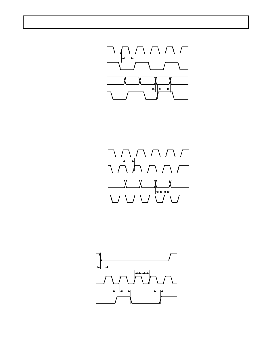
TIMING DIAGRAMS
DAC CLOCK
DATACLOCK OUTPUT
DATACLOCK INPUT
NOTES
1. ALL SIGNALS ARE DIFFERENTIAL (I.E., DAC CLOCK = CLK+ MINUS CLK≠).
2. DATA SET-UP TIME IS THE TIME THAT DATA MUST BE VALID BEFORE THE
DATACLOCK INPUT TRANSITIONS.
3. OPERATION WITH ZERO DATA SET-UP TIME IS THE DEFAULT FOR DDR
(I.E., DATA BUS AND DATACLOCK INPUT TRANSITIONS ARE COINCIDENT).
4. DATA HOLD TIME IS THE TIME THAT DATA MUST REMAIN VALID AFTER
THE DATACLOCK INPUT TRANSITIONS.
5. TYPICALLY DATA BUS IS HELD FOR A FULL CLOCK PERIOD IN DDR, BUT
THIS IS NOT A REQUIREMENT.
6. THE MIMIMUM DATA HOLD TIME IS 0.
DATA BUS
t
DCPD-DDR
t
DSU-DDR
t
DH-DDR
04540-002
Figure 2. DDR Timing Diagram
DAC CLOCK
DATACLOCK OUTPUT
DATACLOCK INPUT
NOTES
1. ALL SIGNALS ARE DIFFERENTIAL (I.E., DAC CLOCK = CLK+ MINUS CLK≠).
2. DATA SET-UP TIME IS THE TIME THAT DATA MUST BE VALID BEFORE THE
RISING EDGE OF THE DATACLOCK INPUT.
3. OPERATION WITH EQUAL DATA SET-UP AND HOLD TIMES IS THE DEFAULT FOR
SDR (I.E., DATACLOCK INPUT IS CENTERED BETWEEN DATA BUS TRANSITIONS).
4. DATA HOLD TIME IS THE TIME THAT DATA MUST REMAIN VALID AFTER
THE RISING EDGE OF THE DATACLOCK INPUT.
5. TYPICALLY DATA BUS IS HELD FOR A HALF CLOCK PERIOD IN SDR, BUT
THIS IS NOT A REQUIREMENT.
6. THE MIMIMUM DATA HOLD TIME IS 0.
DATA BUS
t
DCPD-SDR
t
DSU-SDR
t
DH-SDR
04540-003
Figure 3. SDR Timing Diagram
CSB
SCLK
SDIO (SD0)
t
CPWH
t
DSU
t
DH
t
CPWL
04540-004
SCLK SET-UP TIME
SDIO SET-UP TIME
SDIO HOLD TIME
SDIO (SD0) VALID TIME
SCLK PULSE WIDTH HIGH/LOW TIME
t
CSU
t
DV
Figure 4. SPI Timing Diagram
AD9726
Rev. 0 | Page 8 of 24
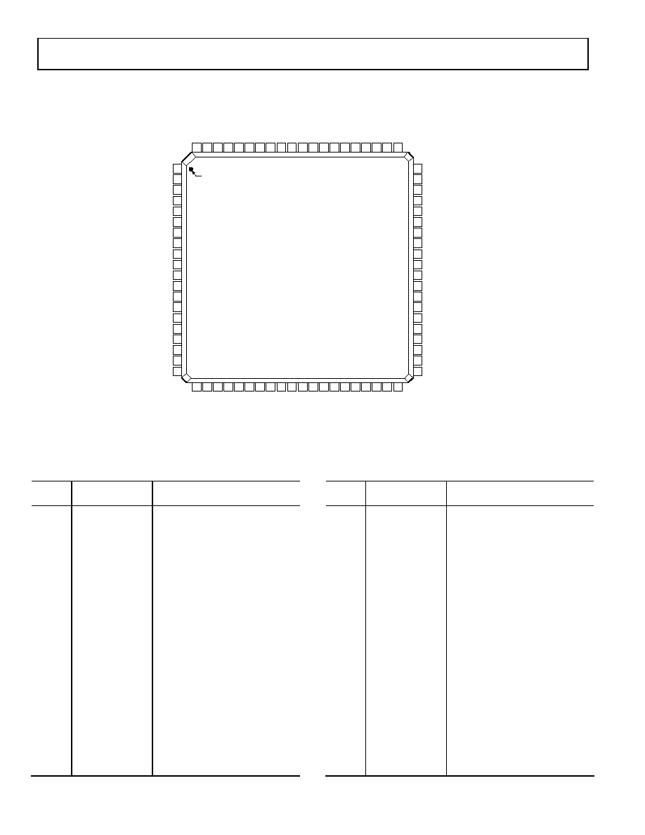
PIN CONFIGURATION AND FUNCTION DESCRIPTIONS
04540-005
2
REXT
3
CLKVDD
4
CLKGND
7
CLKGND
6
CLK≠
5
CLK+
1
CLKVDD
8
DGND
9
DVDD
10
DB15+
12
DB14+
13
DB14≠
14
DB13+
15
DB13≠
16
DB12+
17
DB12≠
18
DB11+
19
DB11≠
20
DBVDD
11
DB15≠
59
58
57
54
55
56
60
53
52
REFIO
RESET
CSB
SDO (SYNCALRM)
SDIO
SCLK (SYNCUPD)
FSADJ
DGND
DVDD
51
DB0≠
49
DB1≠
48
DB1+
47
DB2≠
46
DB2+
45
DB3≠
44
DB3+
43
DB4≠
42
DB4+
DBGND
41
50
DB0+
PIN 1
21
DBGND
22
D
B
10+
23
D
B
10≠
24
DB9
+
25
DB9
≠
26
DB8
+
27
DB8
≠
28
DCLK_
OUT+
29
DCLK_
OUT≠
30
DBV
DD
31
DBGND
32
DCLK_
IN+
33
DCLK_
IN≠
34
DB7
+
35
DB7
≠
36
DB6
+
37
DB6
≠
38
DB5
+
39
DB5
≠
40
DBV
DD
80
SPI_D
IS
79
ADV
DD
78
ADGND
77
ACV
DD
76
ACGND
75
AV
DD2
74
AGND2
73
AV
DD1
72
AGND1
71
IOUTA
70
IOUTB
69
AGND1
68
AV
DD1
67
AGND2
66
AV
DD2
65
ACGND
64
ACV
DD
63
ADGND
62
ADV
DD
61
S
DR_
E
N
AD9726
TOP VIEW
(Not to Scale)
Figure 5: Pin Configuration
Table 6. Pin Function Descriptions
Pin
No. Mnemonic
Description
1 CLKVDD
Clock
Supply
Voltage
2
REXT
Sets Dataclock Output Drive
1
3 CLKVDD
Clock
Supply
Voltage
4
CLKGND
Clock Supply Common
5
CLK+
DAC Clock Input True
6
CLK-
DAC Clock Input Complement
7
CLKGND
Clock Supply Common
8
DGND
Digital Supply Common
9 DVDD
Digital
Supply
Voltage
10
DB15+
Data Bit 15 True
11
DB15-
Data Bit 15 Complement
12
DB14+
Data Bit 14 True
13
DB14-
Data Bit 14 Complement
14
DB13+
Data Bit 13 True
15
DB13-
Data Bit 13 Complement
16
DB12+
Data Bit 12 True
17
DB12-
Data Bit 12 Complement
18
DB11+
Data Bit 11 True
19
DB11-
Data Bit 11 Complement
20
DBVDD
Data Bus Supply Voltage
21
DBGND
Data Bus Supply Common
Pin
No. Mnemonic
Description
22
DB10+
Data Bit 10 True
23
DB10-
Data Bit 10 Complement
24
DB9+
Data Bit 9 True
25
DB9-
Data Bit 9 Complement
26
DB8+
Data Bit 8 True
27
DB8-
Data Bit 8 Complement
28 DCLK_OUT+ Dataclock
Output
True
29
DCLK_OUT-
Dataclock Output Complement
30
DBVDD
Data Bus Supply Voltage
31
DBGND
Data Bus Supply Common
32 DCLK_IN+
Dataclock
Input
True
33
DCLK_IN-
Dataclock Input Complement
34
DB7+
Data Bit 7 True
35
DB7-
Data Bit 7 Complement
36
DB6+
Data Bit 6 True
37
DB6-
Data Bit 6 Complement
38
DB5+
Data Bit 5 True
39
DB5-
Data Bit 5 Complement
40
DBVDD
Data Bus Supply Voltage
41
DBGND
Data Bus Supply Common
42
DB4+
Data Bit 4 True
AD9726
Rev. 0 | Page 9 of 24
Pin
No. Mnemonic
Description
43
DB4-
Data Bit 4 Complement
44
DB3+
Data Bit 3 True
45
DB3-
Data Bit 3 Complement
46
DB2+
Data Bit 2 True
47
DB2-
Data Bit 2 Complement
48
DB1+
Data Bit 1 True
49
DB1-
Data Bit 1 Complement
50
DB0+
Data Bit 0 True
51
DB0-
Data Bit 0 Complement
52 DVDD
Digital
Supply
Voltage
53
DGND
Digital Supply Common
54
SDO
(SYNCALRM)
SPI Data Output (SYNCALRM)
2
55
SDIO
SPI Data Input/Output
3
56
SCLK (SYNCUPD)
SPI Clock Input (SYNCUPD)
4
57
CSB
SPI Chip Select Bar (Active Low)
58
RESET
Hardware Reset (Active High)
59
REFIO
Internal Reference Input/Output
5
60
FSADJ
Output Current Full-Scale Adjust
6
61
SDR_EN
Single Data Rate Mode Enable
7
62 ADVDD
Analog
Supply
Voltage
63 ADGND
Analog
Supply
Common
64 ACVDD
Analog
Supply
Voltage
65 ACGND
Analog
Supply
Common
Pin
No. Mnemonic
Description
66 AVDD2
Analog
Supply
Voltage
67 AGND2
Analog
Supply
Common
68 AVDD1
Analog
Supply
Voltage
69 AGND1
Analog
Supply
Common
70 IOUTB
Analog Current Output
Complement
71
IOUTA
Analog Current Output True
72 AGND1
Analog
Supply
Common
73 AVDD1
Analog
Supply
Voltage
74 AGND2
Analog
Supply
Common
75 AVDD2
Analog
Supply
Voltage
76 ACGND
Analog
Supply
Common
77 ACVDD
Analog
Supply
Voltage
78 ADGND
Analog
Supply
Common
79 ADVDD
Analog
Supply
Voltage
80
SPI_DIS
Serial Port Interface Disable
8
1
Nominally 1 K to DBGND (may be omitted if dataclock output is unused).
2
SDO is output in 4-wire SPI mode and three-state in 3-wire SPI mode. If SPI is
disabled (SPI_DIS = ADVDD), alternate pin function is SYNCALRM output.
3
SDIO is input only in 4-wire SPI mode and bidirectional in 3-wire SPI mode.
4
If SPI is disabled (SPI_DIS = ADVDD), alternate pin function is SYNCUPD.
5
Bypass with 0.1 F to AGND1. Use buffer amp to drive external circuitry.
Limit output current to 1 A. Apply external reference to this pin.
6
Nominally 2 K to AGND1 for 20 mA full-scale output (internal reference).
7
If SPI is disabled, tie pin to ADVDD to enable SDR. Otherwise, tie to ADGND.
8
Tie pin to ADVDD to disable SPI, otherwise, tie to ADGND.

AD9726
Rev. 0 | Page 10 of 24
TERMINOLOGY
Integral Nonlinearity (INL)
Integral nonlinearity error is defined as the maximum deviation
of the actual analog output from the ideal output as determined
by a straight line drawn from zero scale to full scale.
Differential Nonlinearity (DNL)
Differential nonlinearity error is a measure of the maximum
deviation in analog output associated with any single value
change in the digital input code relative to an ideal LSB.
Offset Error
The deviation of the output current from the ideal zero-scale
current is called offset error. For differential outputs, 0 mA is
expected at I
OUTA
when all inputs are low and 0 mA is expected
at I
OUTB
when all inputs are high.
B
Gain Error
The deviation of the output current from the ideal full-scale
current is called gain error. Actual full-scale output current is
determined by subtracting the output when all inputs are low
from the output when all inputs are high.
Output Compliance Range
The range of allowable voltage seen by the analog output of a
current output DAC. Operation beyond the compliance limits
may cause output stage saturation and/or breakdown resulting
in nonlinear performance.
Temperature Drift
Temperature drift is specified as the maximum change in a
parameter from ambient temperature (25∞C) to either T
MIN
or T
MAX
and is typically reported as ppm/∞C.
Spurious-Free Dynamic Range (SFDR)
The difference in decibels between the peak amplitude of a test
tone and the peak amplitude of the largest spurious signal over
the specified bandwidth.
Intermodulation Distortion (IMD)
The difference in decibels between the maximum peak
amplitude of two test tones and the maximum peak amplitude
of the distortion products created from the sum or difference
of integer multiples of the test tones.
Adjacent Channel Leakage Ratio (ACLR)
The ratio between the measured power of a wideband signal
within a channel relative to the measured power in an empty
adjacent channel.
Noise Spectral Density (NSD)
The measured noise power over a 1 Hz bandwidth seen at the
analog output.
Total Harmonic Distortion (THD)
The ratio in decibels of the rms power sum of the first six
harmonic components to the rms power of the output signal.
AD9726
Rev. 0 | Page 11 of 24
TYPICAL PERFORMANCE CURVES
50
60
70
80
90
100
S
F
DR (dBc
)
04540-007
0
12
24
36
48
60
72
84
96
132
120
108
144
f
OUT
(MHz)
≠6dB
0dB
≠3dB
Figure 6. SFDR vs. f
OUT
@ 400 MSPS
50
60
70
80
90
100
S
F
DR (dBc
)
04540-008
0
12
24
36
48
60
7
f
OUT
(MHz)
2
≠6dB
0dB
≠3dB
Figure 7. SFDR vs. f
OUT
@ 200 MSPS
IMD (dBc
)
50
60
80
70
90
100
80
90
100
120 130
30
40
50
60
70
20
110
140
f
OUT
(MHz)
04540-009
f1 + f2 = 0dB
Figure 8. Two-Tone IMD vs. f
OUT
@ 400 MSPS
P
O
W
E
R CONS
UMP
TION (mW
)
550
560
580
570
590
600
620
610
630
100
50
0
150
200
f
OUT
(MHz)
04540-006
SDR
DDR
Figure 9. Power Consumption vs. f
OUT
@ 400 MSPS
A
1AP
EXT
0
≠10
≠20
≠30
≠40
≠60
≠50
≠70
≠90
≠80
≠100
≠120
≠110
1AVG
STOP 7.5MHz
675kHz
START 750kHz
REF LVL
0dBm
40dB
dBm
RF ATT
UNIT
1kHz
1kHz
17s
RBW
VBW
SWT
04540-018
Figure 10. THD @ 400 MSPS and f
OUT
= 1 MHz (Diplexer Low-Pass Output
Showing 0 dBm Fundamental,
See Performance Effects of Calibration Section)
A
1AP
EXT
0
≠10
≠20
≠30
≠40
≠60
≠50
≠70
≠90
≠80
≠100
≠120
≠110
1AVG
STOP 7.5MHz
675kHz
START 750kHz
REF LVL
0dBm
10dB
dBm
RF ATT
UNIT
1kHz
1kHz
17s
RBW
VBW
SWT
04540-019
Figure 11. THD @ 400 MSPS and f
OUT
= 1 MHz (Diplexer High-Pass Output
Showing Harmonics Before Calibration, See Performance Effects of
Calibration Section)
AD9726
Rev. 0 | Page 12 of 24
A
1AP
EXT
0
≠10
≠20
≠30
≠40
≠60
≠50
≠70
≠90
≠80
≠100
≠120
≠110
1AVG
STOP 7.5MHz
675kHz
START 750kHz
REF LVL
0dBm
10dB
dBm
RF ATT
UNIT
1kHz
1kHz
17s
RBW
VBW
SWT
04540-020
Figure 12. THD @ 400 MSPS and f
OUT
= 1 MHz (Diplexer High-Pass Output
Showing Harmonics After Calibration,
See Performance Effects of Calibration Section)
04540-014
SPAN 34.68MHz
SWEEP 1.012s (601 pts)
VBW 100kHz
CENTER 70.00MHz
*RES BW 10kHz
RMS RESULTS
CARRIER POWER
≠14.58dBm/
3.84000MHz
FREQ OFFSET
5.000MHz
10.00MHz
15.00MHz
REF BW
3.840MHz
3.840MHz
3.840MHz
dBc
≠76.72
≠76.96
≠77.07
dBm
≠91.30
≠91.54
≠91.65
LOWER
dBc
≠76.69
≠77.04
≠76.76
dBm
≠91.27
≠91.62
≠91.34
UPPER
REF ≠35dBm
*AVG
Log
10dB/
PAVG
10
W1 S2
*ATTEN 8dB
EXT REF
Figure 13. One-Carrier WCDMA @ 400 MSPS f
OUT
= 70 MHz
04540-015
SPAN 47.38MHz
SWEEP 1.383s (601 pts)
VBW 100kHz
CENTER 70.00MHz
*RES BW 10kHz
1 ≠20.51dBm
2 ≠20.72dBm
TOTAL CARRIER POWER -17.61dBm/7.68000MHz
REF CARRIER POWER -20.72dBm/3.84000MHz
OFFSET FREQ
5.000MHz
10.00MHz
15.00MHz
INTEG BW
3.840MHz
3.840MHz
3.840MHz
dBc
≠70.61
≠71.29
≠71.36
dBm
≠91.34
≠92.01
≠92.08
LOWER
RRC FILTER: ON FILTER ALPHA 0.22
dBc
≠70.74
≠71.31
≠71.06
dBm
≠91.47
≠92.03
≠91.78
UPPER
REF ≠40dBm
*AVG
Log
10dB/
PAVG
10
W1 S2
*ATTEN 6dB
EXT REF
Figure 14. Two-Carrier WCDMA @ 400 MSPS f
OUT
= 70 MHz
04540-016
SPAN 59.58MHz
SWEEP 1.739s (601 pts)
VBW 100kHz
CENTER 70.00MHz
*RES BW 10kHz
1 ≠26.43dBm
2 ≠26.53dBm
3 ≠26.74dBm
4 ≠26.88dBm
TOTAL CARRIER POWER -20.62dBm/15.3600MHz
REF CARRIER POWER -26.43dBm/3.84000MHz
OFFSET FREQ
5.000MHz
10.00MHz
15.00MHz
INTEG BW
3.840MHz
3.840MHz
3.840MHz
dBc
≠66.59
≠67.63
≠67.59
dBm
≠93.00
≠94.04
≠94.00
LOWER
RRC FILTER: ON FILTER ALPHA 0.22
dBc
≠67.07
≠67.54
≠67.44
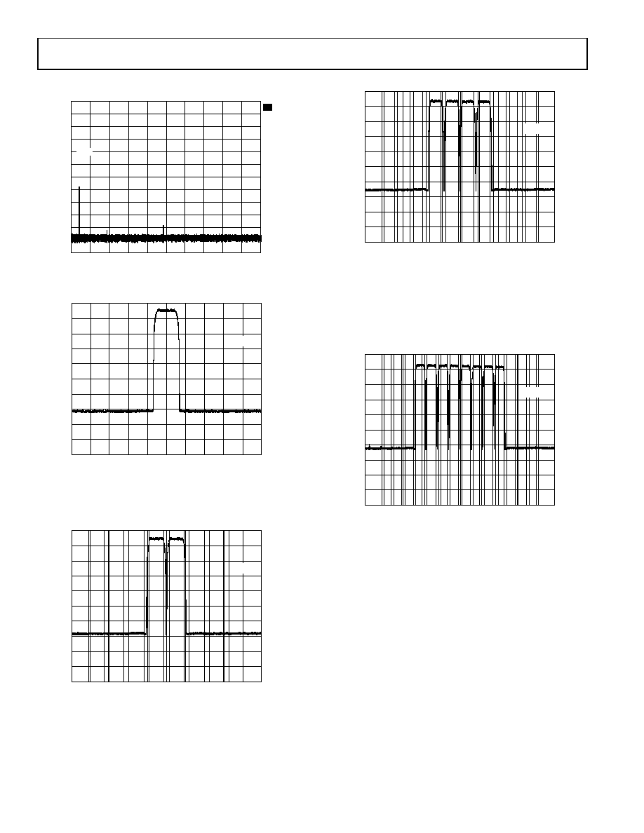
dBm
≠93.48
≠93.95
≠93.86
UPPER
REF ≠45dBm
*AVG
Log
10dB/
PAVG
10
W1 S2
*ATTEN 4dB
EXT REF
Figure 15. Four-Carrier WCDMA @ 400 MSPS f
OUT
= 70 MHz
04540-017
SPAN 83.98MHz
SWEEP 2.451s (601 pts)
VBW 100kHz
CENTER 70.00MHz
*RES BW 10kHz
1 ≠32.21dBm
2 ≠32.30dBm
3 ≠32.44dBm
4 ≠32.59dBm
TOTAL CARRIER POWER -20.62dBm/15.3600MHz
REF CARRIER POWER -26.43dBm/3.84000MHz
OFFSET FREQ
5.000MHz
10.00MHz
15.00MHz
INTEG BW
3.840MHz
3.840MHz
3.840MHz
dBc
≠62.23
≠62.87
≠63.70
dBm
≠94.82
≠95.46
≠96.28
LOWER
RRC FILTER: ON FILTER ALPHA 0.22
dBc
≠62.09
≠62.36
≠62.39
dBm
≠94.68
≠94.94
≠94.98
UPPER
REF ≠50dBm
*AVG
Log
10dB/
PAVG
10
W1 S2
*ATTEN 2dB
EXT REF
Figure 16. Eight-Carrier WCDMA @ 400 MSPS f
OUT
= 70 MHz

AD9726
Rev. 0 | Page 13 of 24
SERIAL PORT INTERFACE
Table 7. SPI Register Map
Addr
Bit 7
Bit 6
Bit 5
Bit 4
Bit 3
Bit 2
Bit 1
Bit 0
0x00 SDIODIR
DATADIR
SWRESET
SLEEP
PWRDWN
EXTREF
0x02 DATAFMT
DATARATE
INVDCLKI
INVDCLKO
DISDCLKO
SYNCMAN
SYNCUPD
SYNCALRM
0x0E
CALMEM[1] CALMEM[0]
CALCLK[2] CALCLK[1] CALCLK[0]
0x0F SCALSTAT
SELFCAL
XFERSTAT
MEMXFER
SMEMWR
SMEMRD
FMEMRD
UNCAL
0x10 MEMADR[7] MEMADR[6] MEMADR[5] MEMADR[4] MEMADR[3] MEMADR[2] MEMADR[1] MEMADR[0]
0x11
MEMDAT[5] MEMDAT[4] MEMDAT[3] MEMDAT[2] MEMDAT[1] MEMDAT[0]
0x15
SYNCOUT[1] SYNCOUT[0]
0x16
SYNCEXT
SYNCIN[1]
SYNCIN[0]
Table 8. SPI Register Bit Default and Descriptions Values
Addr Name
Bit
I/O Default
Description
0x00 SDIODIR
7
I
0
0: SDIO is input only (4-wire SPI mode) and SDO is used for output.
1: SDIO is input/output (3-wire SPI mode) and SDO is unused.
DATADIR 6 I 0
0: SPI serial data byte is MSB first format.
1: SPI serial data byte is LSB first format.
SWRESET
5
I
0
1: Software reset--SPI registers (except 0x00) to default values.
1
SLEEP
4
I
0
1: Analog outputs temporarily disabled.
PWRDWN
3
I
0
1: Full device power-down--all circuits disabled except SPI.
EXTREF
0
I
0
1: Power-down internal reference--use external reference source.
2
0x02 DATAFMT
7
I
0
0: Input data word is twos complement binary format.
1: Input data word is unsigned binary format.
DATARATE 6
I 0
0: DDR mode.
1: SDR mode.
INVDCLKI
5
I
0
1: Inverts polarity of dataclock input.
INVDCLKO
4
I
0
1: Inverts polarity of dataclock output.
DISDCLKO
3
I
0
1: Disables dataclock output.
SYNCMAN
2
I
0
1: Enable sync manual mode--disable automatic update.
SYNCUPD
1
I
0
1: Force manual sync update.
SYNCALRM
0
O
0
1: Indicates sync logic requires update.
0x0E CALMEM
[5:4] O 00
2-bit SMEM contents and calibration status indicator.
00: Uncalibrated--SMEM contains default values (63).
01: Self-calibrated--SMEM contains values from self-calibration.
10: Factory-calibrated--SMEM values transferred from FMEM.
11: User-calibrated--SMEM contains user-entered values.
CALCLK [2:0]
I
000
3-bit self-calibration clock divider ratio. Affects time available for algorithm
settling. Each value increase reduces time by 50%.
3
000: Self-calibration clock is DAC clock/4096 (maximum self-calibration settling
time for highest linearity accuracy).
001,010,011: Self-calibration clock is DAC clock/2048,1024,512.
100,101,110: Self-calibration clock is DAC clock/256,128,64.
111: Self-calibration clock is DAC clock/32 (minimum self-calibration settling
time for fastest algorithm completion).
0x0F
SCALSTAT
7
O
0
1: Indicates completion of self-calibration cycle.
SELFCAL
6
I
0
1: Initiates self-calibration cycle.
4
XFERSTAT
5
O
0
1: Indicates completion of memory transfer cycle.
MEMXFER
4
I
0
1: Initiates FMEM to SMEM transfer.
5
SMEMWR
3
I
0
1: Enable static memory (SMEM) write operation.
SMEMRD
2
I
0
1: Enable static memory (SMEM) read operation.
FMEMRD
1
I
0
1: Enable factory memory (FMEM) read operation.
UNCAL
0
I
0
1: Enable uncalibrated operation--all SMEM to default values..
6
0x10
MEMADR
[7:0]
I
00000000
8-bit memory address value for read/write operations.
0x11
MEMDAT
[5:0]
I/O
000000
6-bit memory data value for read/write operations.

AD9726
Rev. 0 | Page 14 of 24
Addr Name
Bit
I/O Default
Description
0x15
SYNCOUT
[2:0]
O
00
2-bit output value indicates current sync quadrant.
SYNCEXT
5
I
0
1: Enable sync external mode--disable auto quadrant select.
0x16
SYNCIN
[4:3]
I
00
2-bit input value used to specify sync quadrant.
1
SWRESET also resets itself. SMEM contents are unaffected by SWRESET; however, CALMEM reports an uncalibrated state.
2
EXTREF is optional since the internal reference circuit is designed to be overdriven by an external source.
3
The self-calibration clock is also used for the memory transfer cycle; therefore, the CALCLK value affects the MEMXFER process time.
4
Register Bits 3:0 must all be 0 to assert SELFCAL. The time required for the self-calibration cycle is ~100 ms at 100 MHz with CALCLK = 0.
5
Register Bits 3:0 must all be 0 to assert MEMXFER. The time required for the memory transfer cycle is ~15 ms at 100 MHz with CALCLK = 0.
6
The UNCAL bit remains asserted after the cycle completes (SMEM contents held at default values) until the bit is cleared by the user.
AD9726
Rev. 0 | Page 15 of 24
THEORY OF OPERATION
The AD9726 uses LVDS for input data to enable high sample
rates and high performance. LVDS technology uses differential
signals for noise rejection and small signal amplitude for fast
speed with lower power. Each LVDS input on the AD9726 has
an internal 100 active load for proper termination.
DAC CLOCK AND DATACLOCK OUTPUT
The AD9726 uses two clock inputs and offers one clock output.
All are differential signals.
The AD9726 is driven by a master input clock that initiates con-
version and controls all on-chip activity. This signal is referred
to as the DAC clock. It is not LVDS and the CLK+ and CLK≠
pins are high impedance inputs.
The DAC clock is then used to generate the dataclock output.
The DCLK_OUT+ and DCLK_OUT≠ pins form an LVDS
signal that can be used to drive an external FPGA or another
data pump. In SDR mode, the dataclock output always runs at
the same frequency as the DAC clock. In DDR mode, the
dataclock output always runs at Ω the DAC clock frequency.
Use of the dataclock output is optional. It is meant to serve as a
convenient means of regulating the incoming data stream. The
driver can be loaded by a 100 differential termination. An
external 1 k resistor from the REXT pin to DBGND is also
required to set the drive strength. If unused, the dataclock
output pins can be left unconnected and the 1 k resistor at
REXT can be omitted.
The dataclock output can also be inverted by asserting the
INVDCLKO bit in SPI Register 0x02 or the driver can be
disabled by asserting the DISDCLKO bit in the same register.
DATACLOCK INPUT
The remaining clock signal associated with the AD9726 is the
dataclock input. This LVDS signal is not optional and must
accompany the 16-bit data bus. The dataclock input is used to
latch incoming data into the synchronization (sync) logic.
The dataclock input always runs at the same frequency as the
dataclock output in both SDR and DDR modes. A logical
inversion can be accomplished by asserting the INVDCLKI bit.
Driving the DAC Clock Inputs
The DAC clock must be precise and spectrally pure to ensure
the highest ac performance. A symmetrical 50% duty cycle
should be maintained at all times.
The CLK+ and CLK≠ input pins should be driven by a signal
with a common-mode voltage near Ω of CLKVDD. From this
point, peak-to-peak signal amplitude should swing over a range
of at least several hundred millivolts.
04540-
012
CLK+
VCC ≠ 2V
MC100LVEP16
VCC = CLKVDD = 2.5V
VBB = 1.0V
1:1
50
50
CLK≠
AD9726
25
25
Figure 17. Active DAC Clock Drive Circuit
The circuit option shown in Figure 17 uses a receiver/driver IC
from the 2.5 V LVPECL logic family to provide complementary
outputs that fall within these guidelines. A transformer helps
ensure a 50% duty cycle and provides a single-ended to
differential conversion at the input.
The LVPECL device can be conveniently powered from the
same power supply as CLKVDD. The center tap of the trans-
former secondary must be held at 1 V, the switching threshold
of the receiver/driver inputs (use a resistive divider to generate
this voltage or use the internal VBB source with a buffer
amplifier). Based on a 1:1 impedance ratio, 25 resistors across
the secondary provide a matched load to a 50 source.
The driver outputs are terminated as close as possible to the
AD9726 with 50 to VCC - 2 V (or use 75 to 0 V for similar
output levels). Controlled impedance PCB traces should be
used to minimize reflections. Signal levels at the CLK+ and
CLK≠ pins transition between a high near 1500 mV to a low
near 750 mV.
0.1
F
0.1
F
04540-013
CLK+
VDC BIAS = 1.25V
1:1
50
CLK≠
AD9726
Figure 18. Passive DAC Clock Drive Circuit
An alternative circuit option for driving the DAC clock inputs
employs a transmission line transformer (balun) to accomplish
the single-ended to differential conversion. This all-passive
circuit is considerably simpler and less costly, but provides
acceptable performance over a limited range of frequencies.
In this implementation, a sinewave (or other single-ended
source) is coupled directly to the differential DAC clock inputs
through a 50 transformer. Capacitors are used for isolation
and each pin must be dc-biased to a level of 1.25 V (a pair of
simple resistive dividers can be used).

AD9726
Rev. 0 | Page 16 of 24
The 50 termination resistor should be placed as close as pos-
sible to the input pins and controlled impedance PCB traces
should be used.
Good ac performance can be expected from either the active or
passive DAC clock drive circuit. However, in a passive circuit,
the output slew rate is dependent on the frequency of the input,
whereas an active circuit provides consistently high output slew
rates over a wide range of input frequencies.
DATA SYNCHRONIZATION CIRCUITRY
The high performance of the AD9726 requires maintaining
synchronization between the incoming bits and the DAC clock
used to sample and convert the data. Despite the inherent dif-
ficulty in specifying the phase relationship of the DAC clock
and the LVDS dataclock input and the challenge presented by
the high operating speed of the interface, the AD9726 contains
real time logic to automatically monitor and align the data bus
with the DAC clock.
Whether in SDR or DDR mode, input data is always provided
at the same rate. Furthermore, the rate of incoming data always
equals the frequency period of the DAC clock. The data rate
and the DAC clock must also be frequency locked. To accom-
plish this, the primary purpose of the dataclock output is to
provide a time base for data that is derived directly from the
DAC clock.
The function of the dataclock input is to latch incoming data
into the sync block. From there, it is the function of the syn-
chronization logic to position the data with respect to the DAC
clock for optimal ac performance.
Individual data bits must maintain close alignment with one
another such that PCB traces should have matched delays
across the width of the 16-bit bus. In addition, a fixed set-up
and hold timing relationship between the dataclock input and
the data bus is required.
However, because of the sync logic, the phase relationship
between the data bus and the DAC clock is internally opti-
mized. Furthermore, should the phase between the data
bus and the DAC clock drift over time or temperature, the sync
logic automatically updates and adjusts for it. Once synchroni-
zation has been reached, the phase between the data bus and the
DAC clock can vary by a full cycle without loss or corruption of
data.
More detailed explanations of sync operation and optional
programmable modes are presented in the Sync Logic
Operation and Programming section, which also includes an
explanation of how to use the sync logic without the SPI.
ANALOG OUTPUT
The AD9726 is based around a high dynamic range CMOS
core. The analog output consists of differential current sources
each capable of up to 20 mA full scale. Discrete output devices
are PMOS and capable of sourcing current into an output
termination within a compliance voltage range of ±1 V.
In a typical application, both outputs drive discrete resistors-to-
analog ground. From there, especially for higher frequency
outputs, they feed the center-tap secondary of a 1:1 RF trans-
former. A differential-to-single-ended conversion is accom-
plished that provides added gain and cancellation of even
ordered harmonics.
25
≠3dBm
25
I
OUTA
I
OUTB
04540-
021
Figure 19. Transformer Output Circuit
For maximum output power, resistor values can be increased to
50 to provide up to 0 dBm into a 50 load without loss of
performance for most transformers.
04540-011
R
GA
50
I
OUTA
R
FA
R
GB
50
I
OUTB
R
FB
NOTES
1. USE RF AND RG TO SET GAIN
AND LIMIT BANDWIDTH
Figure 20. Op Amp Output Circuit
As an alternative, an active output stage can be used in the
classic instrumentation amplifier configuration. Here, each
DAC output feeds the noninverting input of one of ADI's high-
speed transimpedance op amps.
INTERNAL REFERENCE AND FULL-SCALE OUTPUT
The AD9726 contains an internal 1.2 V precision reference
source; this reference voltage appears at the REFIO pin. It can
be used to drive external circuitry if properly buffered.
Apply an external reference voltage source to the REFIO pin if
desired. The internal source is designed to be easily overdriven
by an external source; however, the internal reference can also
be powered down using the EXTREF bit in SPI Register 0x00.
AD9726
Rev. 0 | Page 17 of 24
The reference voltage (either internal or external) is applied to
an external precision resistor at the FSADJ pin. The resulting
current is internally amplified to provide the full-scale current
at the DAC output according to the following equation:
I
OUTFS
= VREF/R
FSADJ
◊ 32
Taking into account the binary value appearing at the data bus
inputs, the output currents I
OUTA
and I
OUTB
can be determined
according to the following equations:
B
I
OUTA
= I
OUTFS
◊ DB[15:0]/65536
I
OUTB
= I
B
OUTFS
◊ (1 - DB[15:0])/65536
Note that the AD9726 features nonvolatile factory calibrated
gain using the internal reference source and a precision 2 k
load. Gain accuracy in any application is therefore dependent
upon the accuracy of R
FSADJ
.
RESET
Following initial power up and application of a valid DAC clock
signal, the AD9726 should always be given a hardware reset
pulse (active high). This defaults the programmable registers,
initializes the volatile calibration memory, and prepares the
synchronization logic for data. Following the hardware reset,
LVDS data can flow.
The default state of the AD9726 is DDR and twos complement
binary input data. To use the AD9726 in this mode, it is not
necessary to program the device. However, the SPI is also
enabled by default (in 4-wire MSB justified mode) unless the
SPI_DIS pin is connected high to ADVDD.
SERIAL PORT INTERFACE
The serial port interface is a flexible and synchronous serial
communications port allowing easy interface to many industry
standard microcontroller and microprocessor formats
(including both Motorola SPI and Intel SSR protocols). The
interface provides read/write access to registers that configure
the operation of the AD9726.
The AD9726 SPI supports single- and multiple-byte transfers as
well as MSB- or LSB-justified data formats. The interface can be
configured in 3-wire mode (in which SDIO is bidirectional) or
the default 4-wire mode (in which SDIO and SDO function as
unidirectional data input and data output respectively).
Communication Cycle
All communication cycles have two phases. The first phase
concerns writing an instruction byte into the SPI controller and
always coincides with the first eight rising edges of SCLK. The
instruction byte provides the controller with information
regarding the second phase of the cycle, namely the data
transfer phase. In the instruction byte, there are the number of
data bytes to be transferred (1 to 4), a starting register address,
and a read or write operation indicator bit.
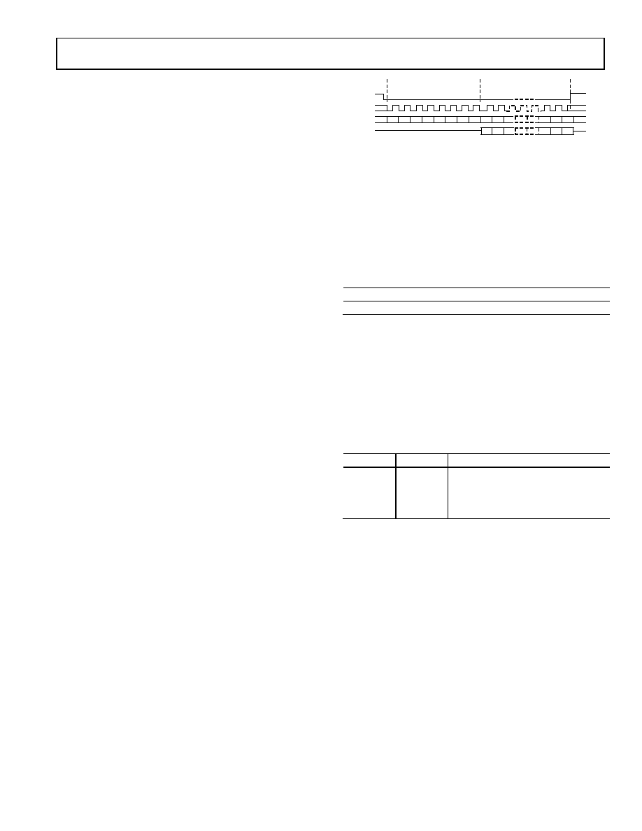
04540-010
CSB
INSTRUCTION CYCLE
DATA TRANSFER CYCLE
SCLK
SDIO
SDO
R/W
N1
N0
A4
A3
A2
A1
A0
D7n D6n
D7n D6n
D20 D10 D00
D20 D10 D00
Figure 21. SPI Communication Cycle
Any communication cycle begins with CSB going low, which
also resets the SPI control logic. Similarly, any communication
cycle ends with CSB going high, which aborts any incomplete
data transfer. Once a communication cycle begins, the next
eight SCLK rising edges interpret data on the SDIO pin as the
instruction byte.
Instruction Byte
The instruction byte bits are detailed in Table 9.
Table 9.
B7 B6 B5 B4 B3 B2 B1 B0
R/W N1 N0 A4 A3 A2 A1 A0
R/W
Bit 7 of the instruction byte selects a read or write transfer. If
the bit is set high, a read operation is indicated. If the bit is low,
a write operation is indicated.
N1, N0
Bit 6 and Bit 5 of the instruction byte determine the number of
data bytes to be transferred, as detailed in Table 10
Table 10.
N1 N0 Description
0 0 Transfer
1
byte
0 1 Transfer
2
bytes
1 0 Transfer
3
bytes
1 1 Transfer
4
bytes
A4, A3, A2, A1, A0
Bit 4 through Bit 0 of the instruction byte define the binary
value of a register address value. For multibyte transfers, this
value is an initial address. The SPI controller increments or
decrements this value to generate successive address values
depending on whether MSB or LSB justification is active.
MSB/LSB Transfers
The SPI can support both MSB- and LSB-justified serial data-
byte formats. This functionality is determined by Bit 6 in SPI
Register 0x00. This bit defaults low, which is MSB justification.
In this mode, serial data bits are written to and/or read from
registers sequentially from Bit 7 to Bit 0.
If Bit 6 of SPI Register 0x00 is set high, the controller switches
to LSB justification. In this mode, data bits are written to or
read from registers sequentially from Bit 0 to Bit 7. Writing to
the instruction bytes is also affected by the active justification.

AD9726
Rev. 0 | Page 18 of 24
For multibyte transfers with MSB justification, the address in
the instruction byte is interpreted as a starting address and its
value is incremented automatically by the controller. For multi-
byte transfers with LSB justification, the address in the instruct-
ion byte is interpreted as an ending address and its value is
decremented automatically by the controller.
Care must be exercised when switching from MSB to LSB
justification. The controller switches modes immediately once
all eight bits of SPI Register 0x00 are written (even if in the
process of a multibyte transfer). For this reason, a single byte
command is recommended when changing justification.
3-Wire and 4-Wire Operation
Bit 7 of SPI Register 0x00 defaults low, enabling 4-wire SPI
operation. In this mode, serial data is input from the SDIO pin
and serial data is output on the SDO pin. Setting Bit 7 of SPI
Register 0x00 high enables 3-wire operation. In this mode,
SDIO becomes bidirectional and switches automatically from
input to output when necessary. The SDO pin in this mode is
unused and assumes a high impedance state.
As with MSB or LSB justification, care must be exercised when
switching operational modes. The change occurs immediately
once all eight bits of SPI Register 0x00 are written.
Writing and Reading Register Data
Bringing CSB low initiates a new communication cycle. The
next eight rising edges of SCLK latch data from SDIO into the
instruction byte. If Bit 7 of the instruction byte is low, a write
operation is enabled. If Bit 7 is high, a read operation is enabled.
For a write operation, a data byte is latched from the SDIO pin
into a register on the next eight rising edges of SCLK. If
instruction byte Bits 6 and 5 are not both 0, a multibyte transfer
latches data bytes into adjacent registers after each successive set
of eight rising SCLK edges. Depending upon MSB or LSB justi-
fication, the controller increments or decrements the address
value in the instruction byte during the cycle as necessary.
If a read operation is enabled, data bits from the addressed
register appear on SDO (or SDIO) with each falling edge of
SCLK. Note that for a read operation, the eighth bit of the
instruction byte is latched on the eighth rising edge of SCLK
and the immediately following falling SCLK edge enables the
first output bit.
For multibyte read sequences, the controller adjusts the register
address when necessary and subsequent data bit values appear
at the output with each falling SCLK edge.
Disabling the SPI
Tie the SPI_DIS pin high to ADVDD to disable the serial port
interface. In this state, the default DDR operational mode can be
changed to SDR by pulling the SDR_EN pin high to ADVDD.
Also, with the SPI disabled, the sync logic no longer operates in
a fully automatic mode. See the Sync Logic Operation and
Programming section for a full explanation of sync operational
modes.
SPI PIN DESCRIPTION
The AD9726 SPI logic runs from the DBVDD supply rail, and
input/output thresholds are based upon a nominal 3.3 V level.
The maximum frequency of operation is 15 MHz.
Chip Select (CSB)
The CSB pin is an active low input. It begins and ends any
communication cycle and must remain low during the entire
cycle. An incomplete cycle is aborted if CSB is prematurely
returned high .
Serial Clock (SCLK)
The SCLK pin is used to synchronize data to and from the SPI
registers and the controller state machine runs from this input.
It is therefore possible to read and write register data (but not
SMEM/FMEM) without a valid DAC clock. All input data is
registered on the rising edge of SCLK and output data bits are
enabled on the falling edge of SCLK.
Serial Data Input/Output (SDIO)
Data is always written into the SPI on the SDIO pin. In 3-wire
mode however, data is also driven out using this pin. The switch
from input to output occurs automatically between the instruct-
ion and data transfer phases of a read operation. In the default
4-wire mode, SDIO is unidirectional and input only.
Serial Data Output (SDO)
Serial data is driven out on the SDO pin when the SPI is in its
default 4-wire mode. In 3-wire mode (or whenever CSB is high)
SDO is set to a high impedance state.
CALIBRATION
To ensure linearity to the 16-bit level, the AD9726 incorporates
132 calibration DACs (CALDACs), which are used to linearize
the current output transfer function. Each CALDAC is a 6-bit
device and takes its input directly from static memory (SMEM).
There are 127 CALDACs associated with each major transition
of the 16-bit input data word (that is, any transition involving
the upper 7 MSBs). A 128th CALDAC operates on the sum total
of the lower 9 LSBs. The remaining 4 CALDACs (129 to 132)
are used to adjust the DAC's overall transfer function gain.
Linearity CALDACs operate inversely from their input, that is,
as their binary input value increases, the magnitude of their
current contribution seen at the AD9726 output decreases. Gain

AD9726
Rev. 0 | Page 19 of 24
CALDACs are an exception to this. Their contribution seen at
the AD9726 output is in direct proportion to their binary input.
Gain CALDACs are also half strength as compared to linearity
CALDACs but, are intended to be used together as a unit and
thus provide twice the current adjustment range in sum total.
Calibration Memory
During production testing, the linearity of the AD9726 is
measured and optimized. Values for all CALDACs are perma-
nently stored in nonvolatile factory memory (FMEM). At
reset, all factory memory contents are transferred to static
memory. CALMEM indicates a factory calibrated state
(CALMEM = 10b).
It is also possible at anytime to transfer the contents of FMEM
to SMEM by asserting the MEMXFER bit. The XFERSTAT
indicator bit then reports the successful completion of the
transfer cycle and MEMXFER is cleared.
Note that the MEMXFER bit (and SELFCAL) can't be asserted if
any other memory access function is currently enabled (that is,
if any Bit [3:0] of Register 0x0F is high). Attempting to assert
MEMXFER (or SELFCAL) in this case clears any asserted bits
in Register 0x0F, but the requested cycle doesn't commence.
The factory-to-static memory data transfer cycle requires a
number of DAC clock cycles. The total depends on the value of
CALCLK. This value sets a divider used to create a slow version
of the DAC clock, which is intended to extend the settling time
available to the self-calibration cycle. However, this divided
clock is also used to sequence a memory transfer cycle.
The divider is set to its maximum value with CALCLK at its
default value. A memory transfer cycle requires about 15 ms at a
DAC clock frequency of 100 MHz. This time can be reduced by
50% for every increase in the value of CALCLK.
Accessing Calibration Memory
SMEM or FMEM locations can be read at any time by setting
the SMEMRD or FMEMRD bit in SPI Register 0x0F. Address
and data information can be input and/or output through SPI
Registers 0x10 and 0x11, respectively.
SMEM locations can also be written by setting the SMEMWR
bit. Registers 0x10 and 0x11 are again used for addresses and
data. Anytime after the SMEMWR bit has been asserted, the
device reports a user-calibrated state (CALMEM = 11b) until
another action changes the calibration memory status.
To reset static memory at any time, assert the UNCAL bit. All
SMEM locations are then reset to their default values (63).
CALMEM reports an uncalibrated state (CALMEM = 00b).
Note that UNCAL remains asserted (and the contents of SMEM
remains at default values) indefinitely. UNCAL doesn't clear
itself (like SWRESET) and must be cleared by the user.
Note also that although SPI registers don't depend on the DAC
clock (they use SCLK to sequence the controller state machine),
SMEM and/or FMEM access does require a valid DAC clock.
SMEM/FMEM Read/Write Procedures
Static and factory memory is accessed through the SPI, but is
not part of the SPI logic. For this reason, memory access
requires a valid DAC clock while SPI register access does not.
But because the AD9726 SPI is so flexible, allowing single and
multiple byte reads and writes, as well as MSB or LSB justified
data, there are perhaps a number of ways in which a user can
access one or more SMEM or FMEM locations.
To avoid potential errors, the following procedures for accessing
static or factory memory should be followed. These procedures
use only single byte SPI commands to ensure the enabling of
addresses and the sequencing of memory access.
1.
To read from SMEM or FMEM, ensure that Bits [3:0] of
Register 0x0F are clear.
2.
Begin the sequence by writing the memory address value
to Register 0x10 with a single byte SPI write command.
3.
Assert the SMEMRD or FMEMRD bit in Register 0x0F
with another single byte SPI write command.
4.
Import the contents of Register 0x11 using a single byte SPI
read command.
5.
Clear the SMEMRD or FMEMRD bit with another single
byte command.
To write to SMEM,
1.
Ensure that Bits [3:0] of Register 0x0F are clear.
2.
Begin the sequence by writing the data value to
Register 0x11 using a single byte SPI write command.
3.
Assert the SMEMWR bit using a single-byte SPI write
command.
4.
Place the memory address value in Register 0x10 using a
single-byte SPI write command.
5.
Clear the SMEMWR bit with a fourth single byte SPI write
command.
Self Calibration
The AD9726 features an internal self-calibration engine to
linearize the transfer function automatically. This can be very
useful at temperature extremes where factory calibration no
longer applies. The automated cycle can be initiated by asserting
the SELFCAL bit.
The self-calibration process calibrates all linearity and gain
CALDACs based upon a fixed internal reference current. Values

AD9726
Rev. 0 | Page 20 of 24
for all CALDACs are stored in volatile static memory. The
CALSTAT bit indicates the successful completion of the cycle
and the SELFCAL bit is cleared. Following the cycle, the device
reports a self-calibrated state (CALMEM = 01b).
As with MEMXFER, successful assertion of the SELFCAL bit
requires that Bits [3:0] of Register 0x0F be clear. If any of these
bits are asserted (such that an SMEM/FMEM read/write/clear
state is enabled), the self-calibration cycle does not begin.
The time required to self-calibrate is dependent on both the
DAC clock frequency and the value of CALCLK. Because self-
calibration requires more time than ordinary operation, the
DAC clock is divided into a slower version and used to step
through the process. Time made available to the self-calibration
algorithm directly impacts its ability to provide accurate results.
A maximum fixed division ratio (4096) corresponds to the
minimum default value of CALCLK (0). The division ratio can
be decreased by increasing the value of CALCLK. Each increase
in the value of CALCLK reduces the DAC clock division factor
(and therefore the time made available to self-calibration) by
50%. With CALCLK at its maximum value (7), the divide ratio
declines to its minimum value (32).
With CALCLK at its default value, self-calibration requires
approximately 100 ms at a DAC clock frequency of 100 MHz.
This time can be reduced to under 0.8 ms if CALCLK = 7. Time
scales relative to DAC clock frequency.
Performance Effects of Calibration
Harmonic distortion for low frequency outputs is primarily a
function of DAC linearity. Figure 10 to Figure 12 show the
harmonic distortion performance of the AD9726.
Figure 10 shows a 1 MHz full-scale output tone. The output
drives a unique low-pass and high-pass filter called a diplexer.
This type of filter presents a uniform 50 load to the DAC and
splits the output signal into low and high frequency paths. The
diplexer's low-pass output passes the 1 MHz fundamental but
attenuates higher frequencies, and the diplexer's high-pass out-
put passes higher frequencies and attenuates the 1 MHz funda-
mental. Figure 10 also shows the diplexer's low pass output.
Here the noise floor is higher than the harmonic distortion
because with a high power input signal, attenuation is required
by the spectrum analyzer.
Figure 11 shows the diplexer's high pass output where the
attenuated input signal can be seen. The spectrum analyzer
attenuation has also been reduced, which lowers the noise
floor. Harmonic products at integer multiples of the funda-
mental are thus revealed. This is the response using the
AD9726 in an uncalibrated state.
Figure 12 shows a response using the AD9726 in a calibrated
state. Harmonic distortion due to the nonlinearities of the
digital-to-analog conversion have virtually been eliminated.
SYNC LOGIC OPERATION AND PROGRAMMING
Recall that a fixed set-up and hold timing relationship between
the dataclock input and the data bus must be established and
maintained. Recall also that the data bus and the DAC clock
must be frequency locked. Because of the sync logic, however,
the phase relationship between the data bus and the DAC clock
is internally optimized. Therefore, data arrival propagation
delays and concern about data transitions near the sampling
instant are eliminated.
Synchronization is automatically enabled upon reset. Once data
arrives and synchronization has been achieved, the sync logic
continuously monitors itself such that should phase drifts occur
over time and/or temperature, automatic adjustments are made.
It is important to note that the sync function and operation of
the sync logic block is transparent, automatic, and ongoing. No
programming is required. For applications where it is useful,
however, the following programmable control is provided.
SYNC Operating States
The sync logic can operate in one of three possible modes. The
default mode is fully automatic.
Fully automatic synchronization is accomplished by demulti-
plexing the incoming data stream into four channels, each
containing every fourth data word. Data words are present for
four DAC clock cycles. Data is remultiplexed by sampling each
channel with the optimum DAC clock cycle.
Initial synchronization is first established through a hardware
reset. This also fully enables the synchronization logic to mon-
itor and resynchronize, as necessary. The AD9726 resynchro-
nizes only if conditions change enough to alter the phase
between the data bus and the DAC clock by more than one full
clock cycle. In this event, an internal alarm occurs and is
followed by an automatic update. During resynchronization,
two data words are typically lost or repeated.
Other than fully automatic mode, two semi-automatic modes
are available.
Sync Manual Mode
In fully automatic mode, the AD9726 both detects when a
resynchronization is necessary and initiates an update. In
manual mode, automatic updating is disabled. Enable manual
mode by setting the SYNCMAN bit in SPI Register 0x02.
In manual mode, the sync logic still monitors incoming data and
the DAC clock, but indicates the need for an update by asserting
the SYNCALRM bit. In this mode, the user is expected to regularly
poll the SYNCALRM bit. When this bit is read back high, the
user can issue a manual sync update also by asserting the
SYNCUPD bit in SPI Register 0x02.

AD9726
Rev. 0 | Page 21 of 24
SYNCALRM does not indicate that data is being lost but that
conditions are close to the point where data may be lost. The
sync logic should be resynchronized by asserting SYNCUPD at
the next convenient time.
In manual mode, users can choose when to update the sync
logic. When operating with burst data, issuing a sync update
between active bursts updates the system without risking the
loss of any data. In fact, since SYNCUPD always forces a resyn-
chronization regardless of operational mode, even users in fully
automatic mode can reduce the possibility of data loss by
occasionally forcing a sync update during idle activity.
If either the dataclock or the DAC clock is interrupted for any
reason, a SYNCUPD should always be executed to ensure that
data bus and DAC clock phase alignment remains optimized.
SYNC External Mode
Going beyond manual mode, sync external mode offers a
greater level of control and can be useful if multiple DAC
channels are employed in an application. Enable sync external
mode by asserting the SYNCEXT bit in SPI Register 0x16.
Manual mode must also be enabled.
The four channels into which each incoming data word is
multiplexed are called quadrants. In any mode, the current
quadrant value can always be readback via SYNCOUT (Bits
[1:0] of SPI Register 0x15). At sync update, the logic chooses the
optimal quadrant and refreshes the value of SYNCOUT.
It is also possible to enter a value into SYNCIN (Bits [4:3] of SPI
Register 0x16). When external mode is enabled, the logic oper-
ates as expected, except that the quadrant value in SYNCIN is
used following an update. This can be used to align delays
between multiple device outputs.
Operating With SPI Disabled
If the SPI_DIS pin is connected high to ADVDD and the SPI is
disabled, the sync logic is placed into manual mode.
SYNCALRM status can then be monitored in hardware via the
unused SPI pin SDO (54) and SYNCUPD requests can be
entered in hardware via the unused SPI pin SCLK (56). If these
two pins are connected together, fully automatic sync operation
can be achieved.
AD9726
Rev. 0 | Page 22 of 24
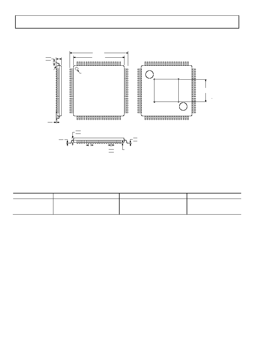
OUTLINE DIMENSIONS
0.15
0.05
0.27
0.22
0.17
0.20
0.09
0.50 BSC
GAGE PLANE
0.25
7∞
3.5∞
0∞
1.05
1.00
0.95
1
20
21
41
40
60
80
61
PIN 1
TOP VIEW
(PINS DOWN)
14.00 SQ
12.00 SQ
SEATING
PLANE
1.20
MAX
0.75
0.60
0.45
1
20
21
41
40
60
80
61
6.00
SQ
BOTTOM
VIEW
COPLANARITY
0.08
COMPLIANT TO JEDEC STANDARDS MS-026-ADD-HD
Figure 22. 80-Lead Thin Plastic Quad Flat Package, Exposed Pad [TQFP/ED]
(SV-80)
Dimensions shown in millimeters
ORDERING GUIDE
Model
Temperature Range
Package Description
Package Option
AD9726BSVZ
1
--40∞C to +85∞C
80-lead TQFP/ED
SV-80
AD9726BSVZ-RL
1
--40∞C to +85∞C
80-lead TQFP/ED
SV-80
AD9728-EB
Evaluation
Board
1
Z = Pb-free part.

AD9726
Rev. 0 | Page 23 of 24
NOTES

AD9726
Rev. 0 | Page 24 of 24
NOTES
© 2005 Analog Devices, Inc. All rights reserved. Trademarks and
registered trademarks are the property of their respective owners.
D04540-0-7/05(0)