 | –≠–ª–µ–∫—Ç—Ä–æ–Ω–Ω—ã–π –∫–æ–º–ø–æ–Ω–µ–Ω—Ç: AD9732 | –°–∫–∞—á–∞—Ç—å:  PDF PDF  ZIP ZIP |

REV. A
Information furnished by Analog Devices is believed to be accurate and
reliable. However, no responsibility is assumed by Analog Devices for its
use, nor for any infringements of patents or other rights of third parties
which may result from its use. No license is granted by implication or
otherwise under any patent or patent rights of Analog Devices.
a
AD9732
One Technology Way, P.O. Box 9106, Norwood, MA 02062-9106, U.S.A.
Tel: 781/329-4700
World Wide Web Site: http://www.analog.com
Fax: 781/326-8703
© Analog Devices, Inc., 1999
10-Bit, 200 MSPS
D/A Converter
FUNCTIONAL BLOCK DIAGRAM
CONTROL
AMP
INTERNAL
VOLTAGE
REFERENCE
SWITCH NETWORK
DECODERS AND DRIVERS
REGISTER
AD9732
D1
D2
D3
D4
D5
D6
D7
D8
D9
D10
CLOCK
R
SET
DIGITAL
+V
S
CONTROL
AMP IN
REF
OUT
CONTROL
AMP OUT
REF
IN
I
OUT
I
OUT
ANALOG
RETURN
TTL
DRIVE
LOGIC
FEATURES
200 MSPS Throughput Rate
3.3 V PECL Digital Input
65 dB SFDR @ 2 MHz A
OUT
, 200 MSPS/54 dB @ 40 MHz
A
OUT
, 200 MSPS
Low Power: 305 mW
Fast Settling: 5 ns to 1/2 LSB
Low Glitch Energy: 6 pVs
Internal Reference
28-Lead SSOP Packaging
APPLICATIONS
Digital Communications
Direct Digital Synthesis
Waveform Reconstruction
High Speed Imaging
GENERAL DESCRIPTION
The AD9732 is a 10-bit, 200 MSPS, bipolar D/A converter that
is optimized to provide high dynamic performance, yet offers
lower power dissipation and a more economical price than pre-
vious high speed DAC solutions. The AD9732 was primarily
designed for demanding communications systems applications
where maximum spurious-free dynamic range (SFDR) is required
at high throughput rates. The proliferation of digital communi-
cations into base station and high volume subscriber-end mar-
kets has created a demand for high performance bipolar DACs
delivered at CMOS associated levels of power dissipation and
cost. The AD9732 is the answer to that demand.
Optimized for direct digital synthesis (DDS) and digital modu-
lator waveform reconstruction, the AD9732 provides >50 dB of
wideband harmonic suppression over the dc to 80 MHz analog
output bandwidth. This signal bandwidth addresses the transmit
spectrum in many of the emerging digital communications ap-
plications where signal purity is critical. Narrowband (
±
1 MHz
window), the AD9732 provides an SFDR of greater than 75 dB.
This level of wideband and narrowband ac performance, coupled
with its 200 MSPS throughput rate, enables the AD9732 to
present outstanding value in the high speed DAC function.
The AD9732 is packaged in a 28-lead SSOP and is specified to
operate over the extended industrial temperature range of ≠40
∞
C
to +85
∞
C. Digital inputs and clock are positive-ECL compatible.

≠2≠
REV. A
AD9732≠SPECIFICATIONS
ELECTRICAL CHARACTERISTICS
(+V
S
= +5 V, ENCODE = 125 MSPS, R
SET
= 1.95 k
(for 20 mA I
OUT
) unless otherwise noted)
Test
AD9732BRS
Parameter
Temp
Level
Min
Typ
Max
Units
THROUGHPUT RATE
+25
∞
C
IV
165
200
MHz
RESOLUTION
10
Bits
DC ACCURACY
Differential Nonlinearity
+25
∞
C
I
0.25
1
LSB
Full
VI
0.36
1
LSB
Integral Nonlinearity
+25
∞
C
I
0.6
1.5
LSB
Full
VI
0.7
1.5
LSB
INITIAL OFFSET ERROR
Zero-Scale Offset Error
+25
∞
C
I
35
70
µ
A
Full
VI
40
100
µ
A
Full-Scale Gain Error
1
+25
∞
C
I
2.5
5
% FS
Full
VI
2.5
5
% FS
Offset Drift Coefficient
V
0.04
µ
A/
∞
C
REFERENCE/CONTROL AMP
Internal Reference Voltage
2
+25
∞
C
I
3.65
3.75
3.85
V
Internal Reference Voltage Drift
Full
IV
150
µ
V/
∞
C
Internal Reference Output Current
3
Full
VI
≠50
+500
µ
A
Amplifier Input Impedance
+25
∞
C
I
50
k
Amplifier Bandwidth
+25
∞
C
I
2.5
MHz
REFERENCE INPUT
4
Reference Input Impedance
+25
∞
C
V
4.6
k
Reference Multiplying Bandwidth
5
+25
∞
C
V
75
MHz
OUTPUT PERFORMANCE
Output Current
4, 6
Full
V
20
mA
Output Compliance
Full
IV
2
5.75
V
Output Resistance
+25
∞
C
V
240
Output Capacitance
+25
∞
C
V
5
pF
Voltage Settling Time to 1/2 LSB (t
ST
)
7
+25
∞
C
V
4.75
ns
Propagation Delay (t
PD
)
8
+25
∞
C
V
2.7
ns
Glitch Impulse
9
Full
V
5.9
pVs
Output Slew Rate
10
Full
V
450
V/
µ
s
Output Rise Time
10
Full
V
1
ns
Output Fall Time
10
Full
V
1
ns
DIGITAL INPUTS
Logic "1" Voltage
Full
VI
2.4
V
Logic "0" Voltage
Full
VI
1.6
V
Logic "1" Current
+25
∞
C
I
1.7
10
µ
A
Logic "0" Current
+25
∞
C
I
≠1
0.01
1
µ
A
Input Capacitance
Full
V
2
pF
Minimum Data Setup Time (t
S
)
11
+25
∞
C
IV
0.7
1.5
ns
Full
IV
1
1.5
ns
Minimum Data Hold Time (t
H
)
12
+25
∞
C
IV
0.7
1.5
ns
Full
IV
1
1.5
ns
Clock Pulsewidth Low (pw
MIN
)
+25
∞
C
IV
2
ns
Clock Pulsewidth High (pw
MAX
)
+25
∞
C
IV
2
ns
POWER SUPPLY
13
Digital +V Supply Current
+25
∞
C
I
15
25
35
mA
Full
VI
10
40
mA
Analog +V Supply Current
+25
∞
C
I
10
20
30
mA
Full
VI
10
30
mA
Power Dissipation
14
+25
∞
C
V
305
mW
Full
V
350
mW
Power Supply Rejection Ratio (PSRR)
+25
∞
C
V
200
µ
A/V

≠3≠
REV. A
AD9732
Test
AD9732BRS
Parameter
Temp
Level
Min
Typ
Max
Units
SFDR PERFORMANCE (Wideband)
15
2 MHz A
OUT
+25
∞
C
V
66
dB
10 MHz A
OUT
+25
∞
C
V
63
dB
20 MHz A
OUT
+25
∞
C
V
57
dB
40 MHz A
OUT
+25
∞
C
V
52
dB
2 MHz A
OUT
(Clock = 165 MHz)
+25
∞
C
V
63
dB
10 MHz A
OUT
(Clock = 165 MHz)
+25
∞
C
V
62
dB
20 MHz A
OUT
(Clock = 165 MHz)
+25
∞
C
V
56
dB
40 MHz A
OUT
(Clock = 165 MHz)
+25
∞
C
V
51
dB
65 MHz A
OUT
(Clock = 165 MHz)
+25
∞
C
V
48
dB
65 MHz A
OUT
(Clock = 200 MHz)
+25
∞
C
V
45
dB
80 MHz A
OUT
(Clock = 200 MHz)
+25
∞
C
V
43
dB
SFDR PERFORMANCE (Narrowband)
15
2 MHz; 2 MHz Span
+25
∞
C
V
77
dB
25 MHz; 2 MHz Span
+25
∞
C
V
65
dB
10 MHz; 5 MHz Span (Clock = 200 MHz)
+25
∞
C
V
70
dB
INTERMODULATION DISTORTION
16
F1 = 800 kHz, F2 = 900 kHz to Nyquist
+25
∞
C
V
69
dB
F1 = 800 kHz, F2 = 900 kHz, Narrowband
(2 MHz)
+25
∞
C
V
61
dB
NOTES
1
Measured as an error in ratio of full-scale current to current through R
SET
(640
µ
A nominal); ratio is nominally 32. DAC load is virtual ground.
2
Internal reference voltage is tested under load conditions specified in Internal Reference Output Current specification.
3
Internal reference output current defines load conditions applied during Internal Reference Voltage test.
4
Full-scale current variations among devices are higher when driving REFERENCE IN directly.
5
Frequency at which a 3 dB change in output of DAC is observed; R
L
= 50
; 100 mV modulation at midscale.
6
Based on I
FS
= 32 ([CONTROL AMP IN ≠ (+V
S
)]/R
SET
) when using internal control amplifier. DAC load is virtual ground.
7
Measured as voltage settling at midscale transition to 0.1%; R
L
= 50
.
8
Measured from 50% point of rising edge of CLOCK signal to 1/2 LSB change in output signal.
9
Peak glitch impulse is measured as the largest area under a single positive or negative transient.
10
Measured with R
L
= 50
and DAC operating in latched mode.
11
Data must remain stable for a specified time prior to rising edge of CLOCK.
12
Data must remain stable for a specified time after rising edge of CLOCK.
13
Supply voltages should remain stable with
±
5% for nominal operation.
14
Power dissipation calculation includes current through a 50
load.
15
SFDR is defined as the difference in signal energy between the full-scale fundamental signal and worst case spurious frequencies in the output spectrum window.
The frequency span dc to Nyquist unless otherwise noted.
16
Intermodulation distortion is the measure of the sum and difference products produced when a two-tone input is driven into the DAC. The distortion products
created will manifest themselves at sum and difference frequencies of the two tones.
Specifications subject to change without notice.
EXPLANATION OF TEST LEVELS
Test Level
I
100% production tested.
II 100% production tested at +25
∞
C and sample tested at
specified temperatures.
III Sample tested only.
IV Parameter is guaranteed by design and characterization
testing.
V
Parameter is a typical value only.
VI 100% production tested at +25
∞
C; guaranteed by design
and characterization testing for industrial temperature
range.
ORDERING GUIDE
Temperature
Package
Package
Model
Range
Description
Option
AD9732BRS
≠40
∞
C to +85
∞
C
28-Lead Small Outline (SSOP)
RS-28
AD9732/PCB
+25
∞
C
Evaluation Board
AD9732
≠4≠
REV. A
CAUTION
ESD (electrostatic discharge) sensitive device. Electrostatic charges as high as 4000 V readily
accumulate on the human body and test equipment and can discharge without detection.
Although the AD9732 features proprietary ESD protection circuitry, permanent damage may
occur on devices subjected to high energy electrostatic discharges. Therefore, proper ESD
precautions are recommended to avoid performance degradation or loss of functionality.
WARNING!
ESD SENSITIVE DEVICE
ABSOLUTE MAXIMUM RATINGS*
Analog Output . . . . . . . . . . . . . . . . . . . . . . . . . . . . . . . . . . +V
S
+V
S
. . . . . . . . . . . . . . . . . . . . . . . . . . . . . . . . . . . . . . . . . +6 V
Digital Inputs . . . . . . . . . . . . . . . . . . . . . . . . . ≠0.7 V to +V
S
Analog Output Current . . . . . . . . . . . . . . . . . . . . . . . . 30 mA
Control Amplifier Input Voltage Range . . . . . . . . . 0 V to +V
S
Reference Input Voltage Range . . . . . . . . . . . . . . . 0 V to +V
S
Internal Reference Output Current . . . . . . . . . . . . . . . 500
µ
A
Control Amplifier Output Current . . . . . . . . . . . . . .
±
2.5 mA
Operating Temperature . . . . . . . . . . . . . . . . . ≠40
∞
C to +85
∞
C
Storage Temperature . . . . . . . . . . . . . . . . . . ≠65
∞
C to +150
∞
C
Maximum Junction Temperature . . . . . . . . . . . . . . . +175
∞
C
Lead Temperature (10 sec) Soldering . . . . . . . . . . . . +300
∞
C
*Stresses above those listed under Absolute Maximum Ratings may cause perma-
nent damage to the device. This is a stress rating only; functional operation of the
device at these or any other conditions outside of those indicated in the operation
sections of this specification is not implied. Exposure to absolute maximum ratings
for extended periods may affect device reliability.
PIN FUNCTION DESCRIPTIONS
Pin Number
Name
Function
1
D9 (MSB)
Most significant data bit of digital input word.
2≠9
D8≠D1
Eight bits of 10-bit digital input word.
10
D0 (LSB)
Least significant data bit of digital input word.
11
CLOCK
TTL-compatible edge-triggered latch enable signal for on-board registers.
12, 13
NC
No internal connection to this pin. Recommend tie to ground.
14, 15, 28
DIGITAL +V
S
+5 V supply voltage for digital circuitry.
16, 22, 27
GND
Converter Ground.
18
ANALOG +V
S
+5 V supply voltage for analog circuitry.
17
R
SET
Connection for external reference set resistor; nominal 1.96 k
. Full-scale output
current = 32 [Control Amp + V
S
] (Reset).
19
ANALOG RETURN
Analog Return. This point and the reference side of the DAC load resistors should be
connected to the same potential (Analog +V
S
).
20
I
OUT
Analog current output; full-scale current occurs with a digital word input of all "1s"
with external load resistor, output voltage = I
OUT
(R
LOAD
R
INTERNAL
). R
INTERNAL
is
nominally 240
.
21
I
OUTB
Complementary analog current output; full-scale current occurs with a digital word
input of all "0s."
23
REF IN
Normally connected to CONTROL AMP OUT (Pin 24). Direct line to DAC current
source network. Voltage changes (noise) at this point have a direct effect on the full-
scale output current of the DAC. Full-scale current output = 32 (CONTROL AMP IN/
R
SET
) when using internal amplifier. DAC load is virtual ground.
24
CONTROL AMP OUT
Normally connected to REF IN (Pin 23). Output of internal control amplifier, which
provides a reference for the current switch network.
25
REF OUT
Normally connected to CONTROL AMP IN (Pin 26). Internal voltage reference,
nominally 3.75 V.
26
CONTROL AMP IN
Normally connected to REF OUT (Pin 25) if not connected to external reference.
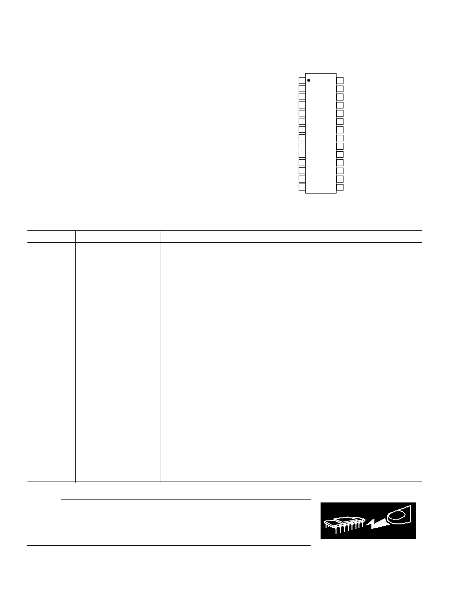
PIN CONFIGURATION
TOP VIEW
(Not to Scale)
28
27
26
25
24
23
22
21
20
19
18
17
16
15
1
2
3
4
5
6
7
8
9
10
11
12
13
14
AD9732
NC = NO CONNECT
DIGITAL +V
S
NC
NC
CLOCK
D0 (LSB)
D1
D2
D9 (MSB)
D8
D7
D6
D3
D4
D5
DIGITAL +V
S
GND
R
SET
ANALOG +V
S
ANALOG RETURN
I
OUT
I
OUTB
DIGITAL +V
S
GND
CONTROL AMP IN
REF OUT
GND
REF IN
CONTROL AMP OUT
AD9732
≠5≠
REV. A
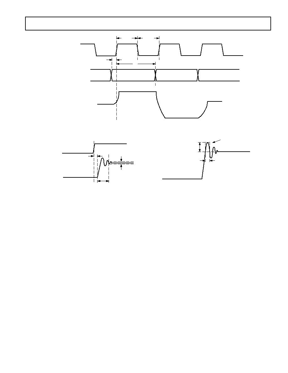
pw
MAX
pw
MIN
t
S
t
H
CODE 1
DATA
CODE 2
DATA
CODE 3
DATA
CODE 4
DATA
CODE 4
CODE 2
CODE 1
CODE 3
CLOCK
DATA
ANALOG OUTPUT
a.
SPECIFIED
ERROR BAND
t
PD
t
ST
CLOCK
ANALOG OUTPUT
DETAIL OF SETTLING TIME
b.
H
W
GLITCH AREA = 1/2 HEIGHT WIDTH
c.
Figure 1. Timing Diagrams
AD9732
≠6≠
REV. A
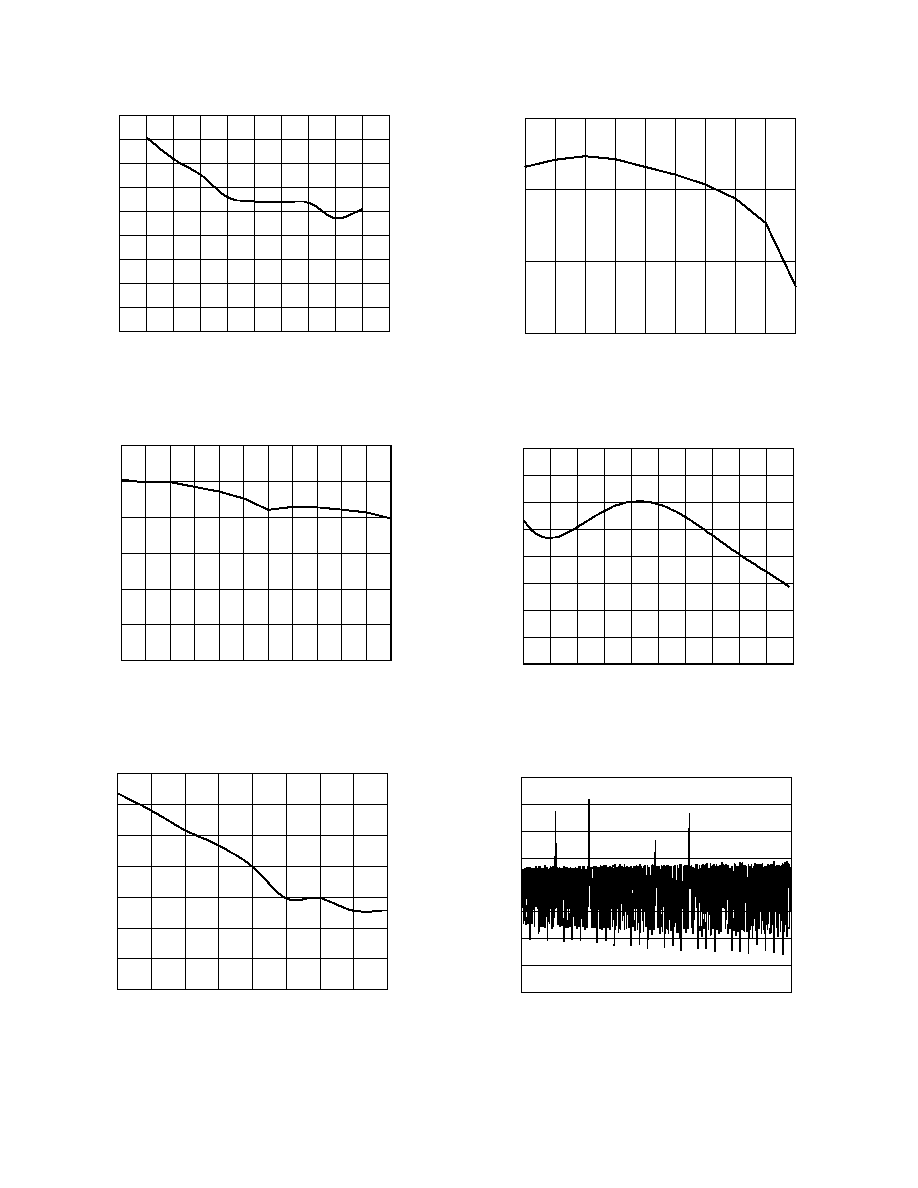
A
OUT
≠ MHz
0
100
10
20
30
40
50
60
70
80
90
75
70
30
SFDR ≠ dB
50
45
40
35
60
55
65
Figure 2. Narrowband SFDR (Clock = 200 MHz) vs. A
OUT
Frequency
A
OUT
≠ MHz
90
60
30
5
60
10
SFDR ≠ dB
15
20
25
30
35
40
45
50
55
80
70
50
40
Figure 3. Narrowband SFDR (Clock = 125 MHz) vs. A
OUT
Frequency
A
OUT
≠ MHz
65
35
10
90
20
SFDR ≠ dB
30
40
50
60
70
80
60
55
50
45
40
30
Figure 4. Wideband SFDR (200 MHz Clock) vs. A
OUT
I
OUT
≠ mA
55
50
40
20
2
18
SFDR ≠ dB
16
14
12
10
8
6
4
45
Figure 5. SFDR vs. I
OUT
CLOCK ≠ MHz
56
46
40
5
145
SFDR ≠ dB
25
45
65
85
105
125
54
48
44
42
52
50
165
185
205
Figure 6. SFDR vs. Clock for f
CLK
/A
OUT
= 3.125
LSB
0.4
≠0.4
≠0.3
≠0.2
≠0.1
0
0.3
0.2
0.1
Figure 7. Typical Differential Nonlinearity Performance
(DNL)
AD9732
≠7≠
REV. A
LSB
0.4
≠0.6
≠0.4
≠0.2
0
0.2
0.6
Figure 8. Typical Integral Nonlinearity Performance (INL)
0
≠60
≠100
START 0Hz
STOP 62.5MHz
6.25MHz/
≠10
≠50
≠70
≠90
≠30
≠40
≠80
≠20
ENCODE = 125MHz
A
OUT
= 2MHz
SPAN = 62.5MHz
SFDR = 66dB
1
1
Figure 9. Wideband SFDR 2 MHz A
OUT
; 125 MHz Clock
0
≠60
≠100
START 0Hz
STOP 62.5MHz
6.25MHz/
≠10
≠50
≠70
≠90
≠30
≠40
≠80
≠20
ENCODE = 125MHz
A
OUT
= 10MHz
SPAN = 62.5MHz
SFDR = 63dB
1
1
Figure 10. Wideband SFDR 10 MHz A
OUT
; 125 MHz Clock
0
≠60
≠100
START 0Hz
STOP 62.5MHz
6.25MHz/
≠10
≠50
≠70
≠90
≠30
≠40
≠80
≠20
ENCODE = 125MHz
A
OUT
= 20MHz
SPAN = 62.5MHz
SFDR = 57dB
1
1
Figure 11. Wideband SFDR 20 MHz A
OUT
; 125 MHz Clock
0
≠60
≠100
START 0Hz
STOP 62.5MHz
6.25MHz/
≠10
≠50
≠70
≠90
≠30
≠40
≠80
≠20
ENCODE = 125MHz
A
OUT
= 40MHz
SPAN = 62.5MHz
SFDR = 52dB
1
1
Figure 12. Wideband SFDR 40 MHz A
OUT
; 125 MHz Clock
0
≠60
≠100
START 0Hz
STOP 100MHz
10MHz/
≠10
≠50
≠70
≠90
≠30
≠40
≠80
≠20
ENCODE = 200MHz
A
OUT
= 40MHz
SPAN = 100MHz
SFDR = 54dB
1
1
Figure 13. Wideband SFDR 40 MHz A
OUT
; 200 MHz Clock
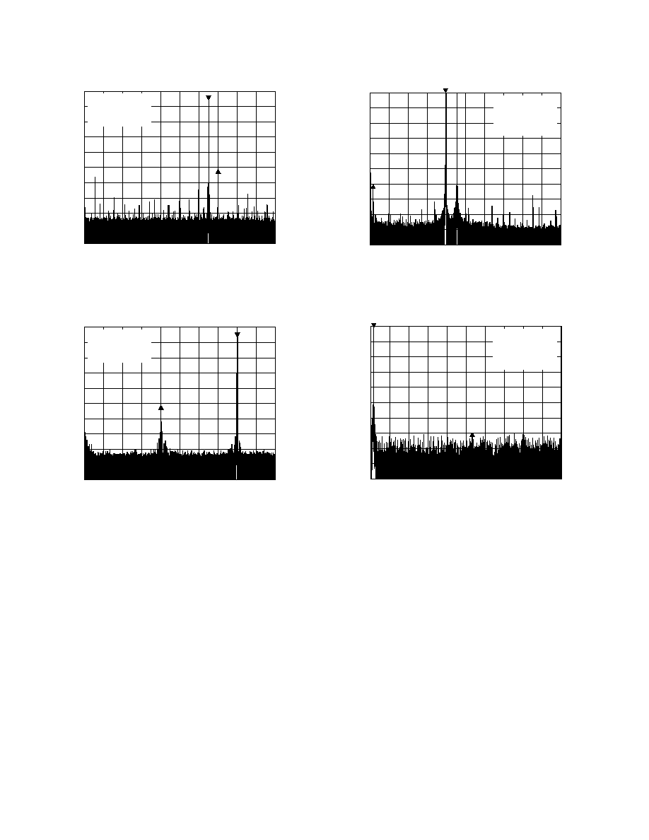
AD9732
≠8≠
REV. A
0
≠60
≠100
START 0Hz
STOP 100MHz
10MHz/
≠10
≠50
≠70
≠90
≠30
≠40
≠80
≠20
ENCODE = 200MHz
A
OUT
= 65MHz
SPAN = 200MHz
SFDR = 45dB
1
1
Figure 14. Wideband SFDR 65 MHz A
OUT
; 200 MHz Clock
0
≠60
≠100
START 0Hz
STOP 100MHz
10MHz/
≠10
≠50
≠70
≠90
≠30
≠40
≠80
≠20
ENCODE = 200MHz
A
OUT
= 80MHz
SPAN = 100MHz
SFDR = 43dB
1
1
Figure 15. Wideband SFDR 80 MHz A
OUT
; 200 MHz Clock
1
START 0Hz
STOP 2MHz
200MHz/
0
≠60
≠100
≠10
≠50
≠70
≠90
≠30
≠40
≠80
≠20
ENCODE = 125MHz
A
OUT
1 = 800kHz
A
OUT
2 = 900kHz
SPAN = 2MHz
IMD = 61dB
1
Figure 16. Wideband Intermodulation Distortion F1 =
800 kHz; F2 = 900 kHz; 125 MHz Clock; Span = 2 MHz
0
≠60
≠100
START 0Hz
STOP 62.5MHz
6.25MHz/
≠10
≠50
≠70
≠90
≠30
≠40
≠80
≠20
ENCODE = 125MHz
A
OUT
1 = 800kHz
A
OUT
2 = 900kHz
SPAN = 62.5MHz
IMD = 69dB
1
1
Figure 17. Wideband Intermodulation Distortion F1 =
800 kHz; F2 = 900 kHz; 125 MHz Clock; Span = 62.5 MHz
AD9732
≠9≠
REV. A
APPLICATION NOTES
THEORY OF OPERATION
The AD9732 high speed digital-to-analog converter utilizes most
significant bit decoding and segmentation techniques to reduce
glitch impulse and deliver high dynamic performance on lower
power consumption than previous bipolar DAC technologies.
The design is based on four main subsections: the decode/driver
circuits, the edge-triggered data register, the switch network and
the control amplifier. An internal bandgap reference is included
to allow operation of the device with minimum external support
components.
Digital Inputs/Timing
The AD9732 has PECL high speed single-ended inputs for data
inputs and clock. The switching threshold is +2.0 V.
In the decode/driver section, the three MSBs are decoded to
seven "thermometer code" lines. An equalizing delay is included
for the seven least significant bits and the clock signals. This
delay minimizes data skew and data setup-and-hold times at the
register inputs.
The on-board register is rising-edge triggered and should be
used to synchronize data to the current switches by applying a
pulse with proper data setup-and-hold times as shown in the
timing diagram. Although the AD9732 is designed to provide
isolation of the digital inputs to the analog output, some cou-
pling of digital transitions is inevitable. Digital feedthrough can
be minimized by forming a low-pass filter at the digital input by
using a resistor in series with the capacitance of each digital
input. This common high speed DAC application technique has
the effect of isolating digital input noise from the analog output.
References
The internal bandgap reference, control amplifier and reference
input are pinned out to provide maximum user flexibility in
configuring the reference circuitry for the AD9732. When using
the internal reference, REF OUT (Pin 25) should be connected
to CONTROL AMP IN (Pin 26). CONTROL AMP OUT (Pin
24) should be connected to REF IN (Pin 23). A 0.1
µ
F ceramic
capacitor connected from Pin 23 to GND improves settling time
by decoupling switching noise from the current sink baseline. A
reference current cell provides feedback to the control amplifier
by sinking current through R
SET
(Pin 17).
Full-scale current is determined by CONTROL AMP IN and
R
SET
according to the following equation:
I
OUT
(FS) = 32 ([CONTROL AMP IN ≠ (+V
S
)]/R
SET
)
The internal reference is nominally ≠1.25 V (referenced to
Analog +V
S
), with a tolerance of
±
8% and typical drift over
temperature of 150 ppm/
∞
C. If greater accuracy or temperature
stability is required, an external reference can be used. The
AD589 reference features 10 ppm/
∞
C drift over the 0
∞
C to
+70
∞
C temperature range.
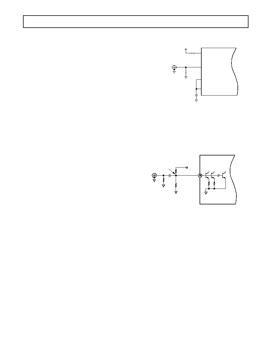
Two modes of multiplying operation are possible with the
AD9732. Signals with bandwidths up to 2.5 MHz and input
swings from 3.8 V to 4.4 V can be applied to the CONTROL
AMP IN pin as shown in Figure 18. Because the control ampli-
fier is internally compensated, the 0.1
µ
F capacitor discussed
above can be reduced to maximize the multiplying bandwidth.
However, it should be noted that output settling time, for
changes in the digital word, will be degraded.
AD9732
R
SET
CONTROL
AMP IN
CONTROL
AMP OUT
REFERENCE IN
R
SET
R
T
3.8V TO 4.4V
2.5MHz TYPICAL
0.1 F
+V
S
Figure 18. Lower Frequency Multiplying Circuit
The REFERENCE IN pin can also be driven directly for wider
bandwidth multiplying operation. The analog signal for this
mode of operation must have a signal swing in the range of
0.95 V to 1.9 V. This can be implemented by capacitively cou-
pling into REFERENCE IN a signal with a dc bias of 1.9 V (I
OUT
= 22.5 mA) to 0.95 V (I
OUT
= 3 mA), as shown in Figure 19, or
by dividing REFERENCE IN with a low impedance op amp
whose signal swing is limited to the stated range.
AD9732
REFERENCE IN
APPROX
1.4V
+V
S
Figure 19. Wideband Multiplying Circuit
Analog Output
The switch network provides complementary current outputs
I
OUT
and I
OUTB
. The design of the AD9732 is based on statisti-
cal current source matching, which provides a 10-bit linearity
without trim. Current is steered to either I
OUT
or I
OUTB
in pro-
portion to the digital input word. The sum of the two currents is
always equal to the full-scale output current. The current can be
converted to a voltage by resistive loading as shown in Figure
20. Both I
OUT
and I
OUTB
should be equally loaded for best over-
all performance. The voltage that is developed is the product of
the output current and the value of the load resistor.
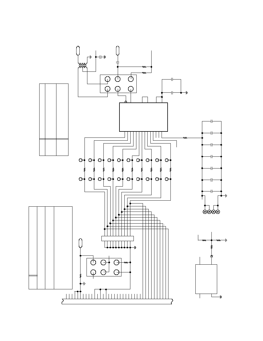
EVALUATION BOARD
The performance characteristics of the AD9732 make it ideally
suited for direct digital synthesis (DDS) and other waveform
synthesis applications. The AD9732 evaluation board provides a
platform for analyzing performance under optimum layout con-
ditions. The AD9732 also provides a reference for high speed
circuit board layout techniques.
AD9732
≠10≠
REV. A
OUT TO 50
LOAD
1
2
3
4
5
6
7
8
9
10
11
12
13
14
15
16
17
18
19
20
21
22
23
24
25
26
27
28
29
30
31
32
33
34
35
36
37
R5
50
E1
E3
E5
E2
E4
E6
1
1
1
1
1
1
CLKB
CLK
R6
50
1
3
5
7
9
11
13
15
17
19
2
4
6
8
10
12
14
16
18
20
H1
J1
BNC
1
2
3
4
5
6
7
8
9
10
11
12
13
17
D9 (MSB)
D8
D7
D6
D5
D4
D3
D2
D1
D0 (LSB)
CLK
NC1
NC2
R
SET
IOUT
I_OUT
REFOUT
C_AMP_IN
C_AMP_OUT
REF_IN
21
20
25
26
24
23
U1
AD9732
1
E20
1
E18
1
E16
1
E14
1
E12
1
E10
1
E8
1
E22
1
E24
1
E26
1
E19
1
E17
1
E15
1
E13
1
E11
1
E5
1
E7
1
E21
1
E23
1
E25
CLK
E27
E29
E31
E28
E32
E30
11
1
1
1
1
3
2
1
4
6
T1≠1T
T1
J3
DAC_OUT
(DIFFERENTIAL)
OUT TO 50
LOAD
C11
0.1
F
+5V
J2
C10
0.1
F
R16
25
R15
50
+5V
DAC_OUT
(SINGLE ENDED)
+
C1
0.1
F
+5V: 14, 15, 18, 19, 28
ANALOG GND 22
DIGITAL GND 16, 27
NOTE:
SERIES 64.9
RESISTORS
CAN BE BYPASSED BY
JUMPING E7 TO E8, ECT.
C7
0.1
F
C6
0.1
F
C5
0.1
F
C4
0.1
F
C3
0.1
F
C2
0.1
F
C9
10
F
+5V
TB1
TB4
1
2
3
4
OSC_OUT
+V
GND
NO_CONN
SW41
Y1
1
7
+5V
CLKB
CR1
1N914
R17
180
R13
780
R14
390
+5V
IN
CMOS CLOCK OSCILLATOR
C37DRPF
P1
SW1
SW2
C8
10
F
R12
64.9
R11
64.9
R10
64.9
R9
64.9
R8
64.9
R4
64.9
R3
64.9
R2
64.9
R1
64.9
R18
64.9
R7
1960
CLOCK MATRIX DESCRIPTION
CONNECTIONS
SW1
1 TO 3 ON BOARD XTAL OSCILLATOR
2 TO 4 BNC EXTERNAL PECL CLOCK (50
)
3 = INPUT PIN FOR EXTERNAL CLOCK
5 = GND PIN FOR EXTERNAL CLOCK
4 TO 6 ADD 50V TERMINATION FOR EXTERNAL CLOCK
OUTPUT DESCRIPTION
SW2
27 TO 29
30 TO 28
DIFFERENTIAL TRANSFORMER
COUPLED TERMINATION
29 TO 32
31 TO 30
SINGLE-ENDED RESISTIVE TERMINATED
14
8
Figure 20. Evaluation Board
AD9732
≠11≠
REV. A
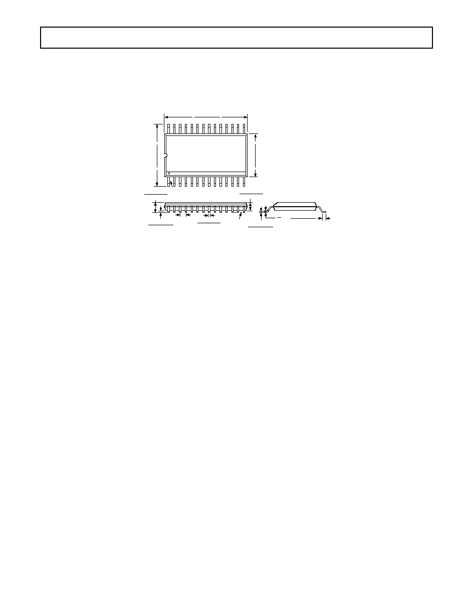
OUTLINE DIMENSIONS
Dimensions shown in inches and (mm).
28-Lead SSOP
(RS-28)
28
15
14
1
0.407 (10.34)
0.397 (10.08)
0.311 (7.9)
0.301 (7.64)
0.212 (5.38)
0.205 (5.21)
PIN 1
SEATING
PLANE
0.008 (0.203)
0.002 (0.050)
0.07 (1.79)
0.066 (1.67)
0.0256
(0.65)
BSC
0.078 (1.98)
0.068 (1.73)
0.015 (0.38)
0.010 (0.25)
0.009 (0.229)
0.005 (0.127)
0.03 (0.762)
0.022 (0.558)
8
0
PRINTED IN U.S.A.
C3365a≠0≠4/99