 | –≠–ª–µ–∫—Ç—Ä–æ–Ω–Ω—ã–π –∫–æ–º–ø–æ–Ω–µ–Ω—Ç: AD9734 | –°–∫–∞—á–∞—Ç—å:  PDF PDF  ZIP ZIP |
10-, 12-, 14-Bit, 1200 MSPS DACS
AD9734/AD9735/AD9736
Rev. 0
Information furnished by Analog Devices is believed to be accurate and reliable.
However, no responsibility is assumed by Analog Devices for its use, nor for any
infringements of patents or other rights of third parties that may result from its use.
Specifications subject to change without notice. No license is granted by implication
or otherwise under any patent or patent rights of Analog Devices. Trademarks and
registered trademarks are the property of their respective owners.
One Technology Way, P.O. Box 9106, Norwood, MA 02062-9106, U.S.A.
Tel: 781.329.4700
www.analog.com
Fax: 781.461.3113
© 2005 Analog Devices, Inc. All rights reserved.
FEATURES
Pin-compatible family
Excellent dynamic performance
AD9736: SFDR = 82 dBc at f
OUT
= 30 MHz
AD9736: SFDR = 69 dBc at f
OUT
= 130 MHz
AD9736: IMD = 87 dBc at f
OUT
= 30 MHz
AD9736: IMD = 82 dBc at f
OUT
= 130 MHz
LVDS data interface with on-chip 100 terminations
Built-in self test
LVDS sampling integrity
LVDS-to-DAC data transfer integrity
Low power: 380 mW (I
FS
= 20 mA; f
OUT
= 330 MHz)
1.8/3.3 V dual-supply operation
Adjustable analog output
8.66 mA to 31.66 mA (RL = 25 to 50 )
On-chip 1.2 V reference
160-lead chip scale ball grid array (CSP_BGA) package
APPLICATIONS
Broadband communications systems
Cellular infrastructure (digital predistortion)
Point-to-point wireless
CMTS/VOD
Instrumentation, automatic test equipment
Radar, avionics
PRODUCT DESCRIPTION
The AD9736, AD9735, and AD9734 are high performance, high
frequency DACs that provide sample rates of up to 1200 MSPS,
permitting multicarrier generation up to their Nyquist
frequency. The AD9736 is the 14-bit member of the family,
while the AD9735 and the AD9734 are the 12-bit and 10-bit
members, respectively. They include a serial peripheral interface
(SPI) port that provides for programming of many internal
parameters and also enables readback of status registers. A
reduced-specification LVDS interface is utilized to achieve the
high sample rate. The output current can be programmed
over a range of 8.66 mA to 31.66 mA. The AD973x family is
manufactured on a 0.18 µm CMOS process and operates from
1.8 V and 3.3 V supplies for a total power consumption of
380 mW in bypass mode. It is supplied in a 160-lead chip scale
ball grid array for reduced package parasitics.
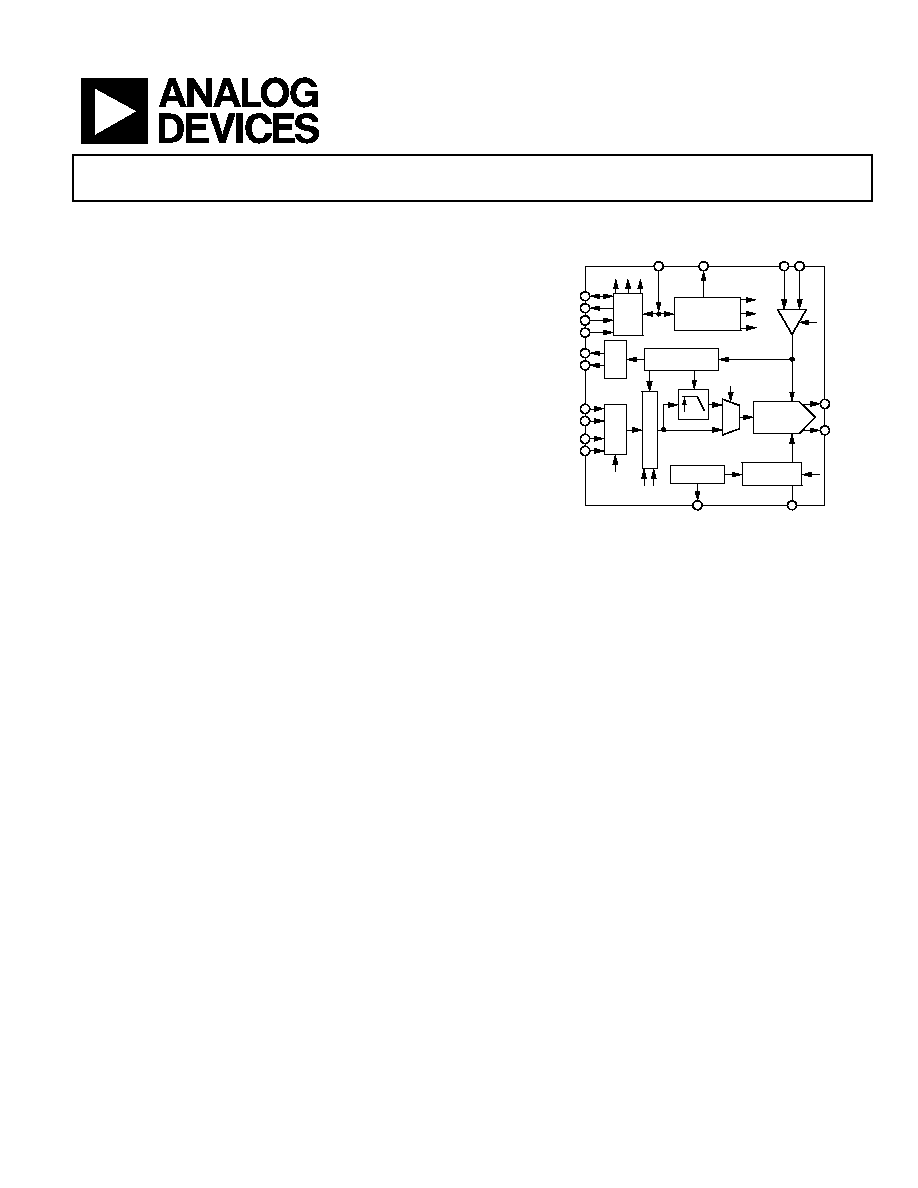
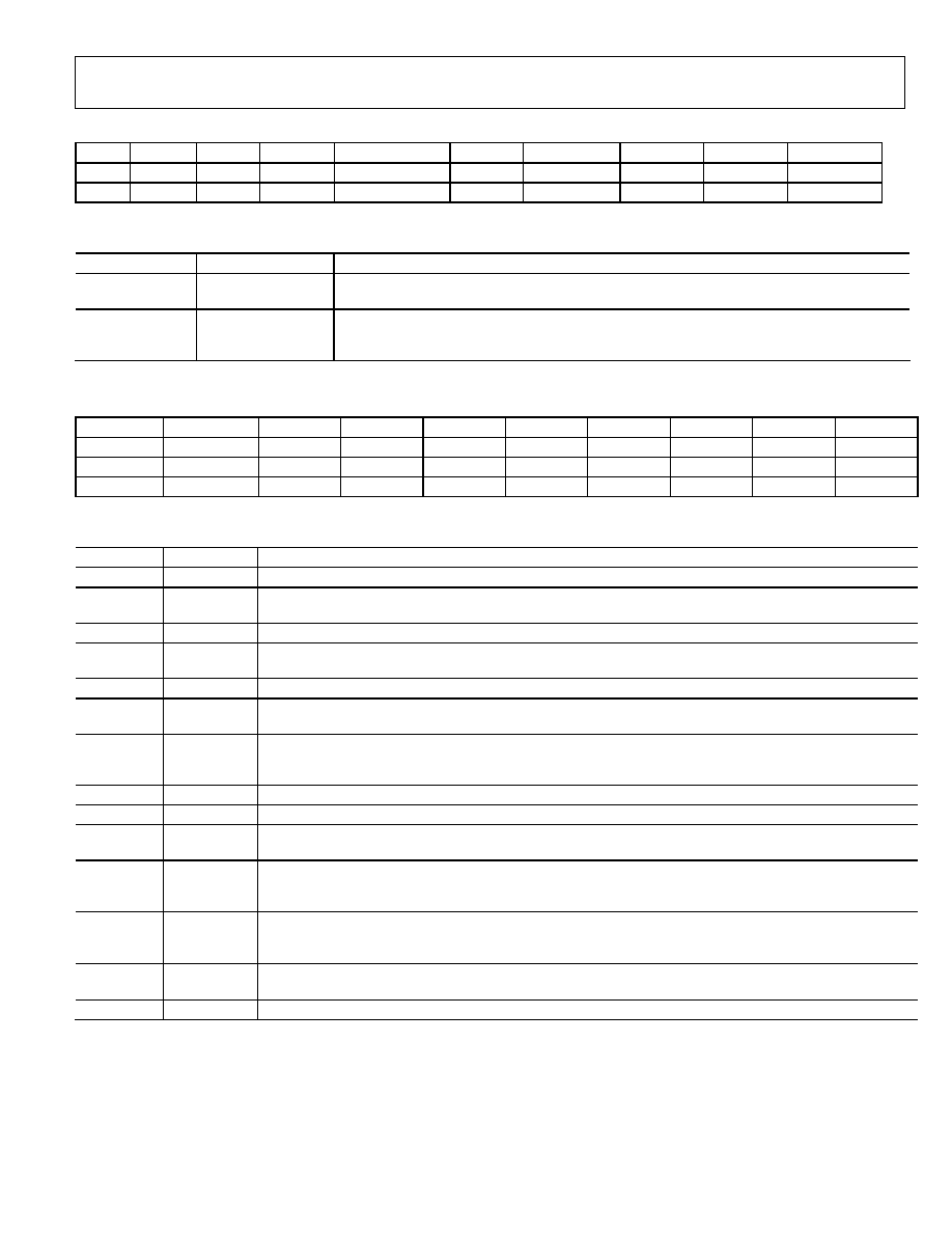
FUNCTIONAL BLOCK DIAGRAM
LVDS
RE
CE
IV
E
R
S
Y
NCHRONIZE
R
BAND GAP
DATACLK_IN+
DATACLK_IN≠
DB[13:0]≠
DB[13:0]+
SPI
14-, 12-,
10-BIT DAC
CORE
IOUTA
IOUTB
SDO
SDI
SCLK
CSB
LVDS
DRIV
E
R
CONTROLLER
REFERENCE
CURRENT
DACCLK≠
IRQ
DACCLK+
I120
VREF
RESET
DATACLK_OUT+
DATACLK_OUT≠
S1 S2 S3
C1
C2
C3
C2
C1S1
S3
S2
C3
04862-001
2◊
CLOCK
DISTRIBUTION
Figure 1.
PRODUCT HIGHLIGHTS
1.
Low noise and intermodulation distortion (IMD) features
enable high quality synthesis of wideband signals at
intermediate frequencies up to 600 MHz.
2.
Double data rate (DDR) LVDS data receivers support the
maximum conversion rate of 1200 MSPS.
3.
Direct pin programmability of basic functions or SPI port
access for complete control of all AD973x family functions.
4.
Manufactured on a CMOS process, the AD973x family
uses a proprietary switching technique that enhances
dynamic performance.
5.
The current output(s) of the AD9736 family are easily con-
figured for single-ended or differential circuit topologies.

AD9734/AD9735/AD9736
Rev. 0 | Page 2 of 68
TABLE OF CONTENTS
DC Specifications ............................................................................. 4
Digital Specifications........................................................................ 6
AC Specifications.............................................................................. 8
Absolute Maximum Ratings............................................................ 9
ESD Caution.................................................................................. 9
Pin Configuration and Function Descriptions........................... 10
Terminology .................................................................................... 13
Typical Performance Characteristics ........................................... 14
AD9736 Static Linearity, 10 mA Full Scale ............................. 14
AD9736 Static Linearity, 20 mA Full Scale ............................. 15
AD9736 Static Linearity, 30 mA Full Scale ............................. 16
AD9735 Static Linearity, 10 mA, 20 mA, 30 mA Full Scale . 17
AD9734 Static Linearity, 10 mA, 20 mA, 30 mA Full Scale . 18
AD9736 Power Consumption, 20 mA Full Scale................... 19
AD9736 Dynamic Performance, 20 mA Full Scale................ 19
AD9736 Dynamic Performance, 20 mA Full Scale................ 21
AD9736, AD9735, AD9734 WCDMA ACLR, 20 mA Full
Scale.............................................................................................. 22
AD9735, AD9734 Dynamic Performance, 20 mA Full Scale24
SPI Register Map............................................................................. 25
SPI Register Descriptions .............................................................. 26
MODE Register (REG 00) ......................................................... 26
Interrupt Request Register (IRQ) (Reg 01)............................. 26
Full Scale Current (FSC) Register (Regs 02, 03)..................... 27
LVDS Controller (LVDS_CNT) Register (Regs 04, 05, 06) .. 27
SYNC Controller (SYNC_CNT) Register (Regs 07, 08) ....... 28
Cross Controller (CROS_CNT) Register (Regs 10, 11) ........ 28
Analog Control (ANA_CNT) Register (Regs 14, 15)............ 29
Built-in Self Test Control (BIST_CNT) Registers (Regs 17, 18,
19, 20, 21) .................................................................................... 29
Controller Clock Predivider (CCLK_DIV) Reading Register
(Reg 22)........................................................................................ 30
Theory of Operation ...................................................................... 31
Serial Peripheral Interface ............................................................. 32
General Operation of the Serial Interface............................... 32
Short Instruction Mode (8-Bit Instruction) ........................... 32
Long Instruction Mode (16-Bit Instruction).......................... 32
Serial Interface Port Pin Descriptions ..................................... 32
MSB/LSB Transfers .................................................................... 33
Notes on Serial Port Operation ................................................ 33
Pin Mode Operation .................................................................. 34
Reset Operation.......................................................................... 34
Programming Sequence ............................................................ 34
Interpolation Filter ..................................................................... 35
Data Interface Controllers......................................................... 35
LVDS Sample Logic.................................................................... 36
LVDS Sample Logic Calibration............................................... 36
Operating the LVDS Controller In Manual Mode via the SPI
Port ............................................................................................... 37
Operating the LVDS Controller in Surveillance and Auto
Mode ............................................................................................ 37
SYNC Logic and Controller .......................................................... 38
SYNC Logic and Controller Operation................................... 38
Operating in Manual Mode ...................................................... 38
Operation in Surveillance and Auto Modes ........................... 38
FIFO Bypass ................................................................................ 38
Digital Built-In Self Test (BIST) ................................................... 40
Overview ..................................................................................... 40
AD973x BIST Procedure........................................................... 41
AD973x Expected BIST Signatures.......................................... 41
Generating Expected Signatures .............................................. 42
Cross Controller Registers............................................................. 43

AD9734/AD9735/AD9736
Rev. 0 | Page 3 of 68
Analog Control Registers ...............................................................44
Band Gap Temperature Characteristic Trim Bits ...................44
Mirror Roll-Off Frequency Control .........................................44
Headroom Bits.............................................................................44
Voltage Reference ........................................................................45
Applications Information...............................................................46
Driving the DACCLK Input ......................................................46
DAC Output Distortion Sources ...................................................47
DC-Coupled DAC Outputs ...........................................................48
DAC Data Sources ..........................................................................49
Input Data Timing ..........................................................................50
Synchronization Timing.................................................................51
Power Supply Sequencing ..............................................................52
AD973
X
Evaluation Board Schematics ........................................53
AD973
X
Evaluation Board PCB Layout.......................................58
Outline Dimensions........................................................................65
Ordering Guide ...........................................................................65
REVISION HISTORY
4/05--Revision 0: Initial Version

AD9734/AD9735/AD9736
Rev. 0 | Page 4 of 68
DC SPECIFICATIONS
AVDD33 = DVDD33 = 3.3 V, CVDD18 = DVDD18 = 1.8 V, maximum sample rate, I
FS
= 20 mA, 1◊ mode, 25 1% balanced load,
unless otherwise noted.
Table 1.
AD9736
AD9735
AD9734
Parameter Min
Typ
Max
Min
Typ
Max
Min
Typ
Max
Unit
RESOLUTION
14
12
10
Bits
ACCURACY
Integral Nonlinearity (INL)
-5.6
±1.0
+5.6
-1.5
±0.50
+1.5
-0.5
±0.12
+0.5
LSB
Differential Nonlinearity (DNL)
-2.1
±0.6
+2.1
-0.5
±0.25
+0.5
-0.1
±0.06
+0.1
LSB
ANALOG
OUTPUTS
Offset Error
-0.01
±0.005
+0.01
-0.01
±0.005
+0.01
-0.01
±0.005
+0.01
% FSR
Gain Error (With Internal
Reference)
±1.0
±1.0
±1.0
%
FSR
Gain Error (Without Internal
Reference)
±1.0
±1.0
±1.0
%
FSR
Full-Scale Output Current
8.66
20.2
31.66
8.66
20.2
31.66
8.66
20.2
31.66
mA
Output Compliance Range
-1.0
+1.0
-1.0
1.0
-1.0
+1.0
V
Output Resistance
10
10
10
M
Output Capacitance
1
1
1
pF
TEMPERATURE
DRIFT
Offset
0
0
0
ppm/∞C
Gain
80 80 80 ppm/∞C
Reference Voltage
1
40
40
40
ppm/∞C
REFERENCE
Internal Reference Voltage
1
1.14
1.2
1.26
1.14
1.2
1.26
1.14
1.2
1.26
V
Output Resistance
2
5 5 5 k
ANALOG SUPPLY VOLTAGES
AVDD33
3.13
3.3
3.47
3.13
3.3
3.47
3.13
3.3
3.47
V
CVDD18
1.70
1.8
1.90
1.70
1.8
1.90
1.70
1.8
1.90
V
DIGITAL SUPPLY VOLTAGES
DVDD33
3.13
3.3
3.47
3.13
3.3
3.47
3.13
3.3
3.47
V
DVDD18
1.70
1.8
1.90
1.70
1.8
1.90
1.70
1.8
1.90
V
SUPPLY CURRENTS
1◊ Mode, 1.2 GSPS
I
AVDD33
25
25
25
mA
I
CVDD18
47
47
47
mA
I
DVDD33
10
10
10
mA
I
DVDD18
122
122
122
mA
FIR Bypass (1◊) Mode
380
380
380
mW
2◊ Mode, 1.2 GSPS
I
AVDD33
25
25
25
mA
I
CVDD18
47
47
47
mA
I
DVDD33
10
10
10
mA
I
DVDD18
234
234
234
mA
FIR 2◊ Interpolation Filter
Enabled
550
550
550
mW
AD9734/AD9735/AD9736
Rev. 0 | Page 5 of 68
AD9736
AD9735
AD9734
Parameter Min
Typ
Max
Min
Typ
Max
Min
Typ
Max
Unit
Static,
No
Clock
I
AVDD33
25
25
25
mA
I
CVDD18
8
8
8
mA
I
DVDD33
10
10
10
mA
I
DVDD18
2
2
2
mA
FIR Bypass (1◊) Mode
133
133
133
mW
Sleep Mode, No Clock
I
AVDD33
2.5 3.15
2.5 3.15
2.5 3.15
mA
FIR Bypass (1◊) Mode
59
65
59
65
59
65
mW
Power-Down
Mode
I
AVDD33
0.01 0.13
0.01 0.13
0.01 0.13
mA
I
CVDD18
0.02 0.12
0.02 0.12
0.02 0.12
mA
I
DVDD33
0.01 0.12
0.01 0.12
0.01 0.12
mA
I
DVDD18
0.01 0.11
0.01 0.11
0.01 0.11
mA
FIR Bypass (1◊) Mode
0.12
1.24
0.12
1.24
0.12
1.24
mW
1
Default band gap adjustment (Reg0E<2:0> = 0h).
2
Use an external amplifier to drive any external load.

AD9734/AD9735/AD9736
Rev. 0 | Page 6 of 68
DIGITAL SPECIFICATIONS
AVDD33 = DVDD33 = 3.3 V, CVDD18 = DVDD18 = 1.8 V, maximum sample rate, I
FS
= 20 mA, 1◊ mode, 25 1% balanced load,
unless otherwise noted.
LVDS drivers and receivers are compliant to the IEEE-1596 reduced range link, unless otherwise noted.
Table 2.
Parameter
Min
Typ
Max
Unit
LVDS DATA INPUTS
(DB[13:0]+, DB[13:0]-) DB+ = V
ia
, DB- = V
ib
Input Voltage Range, V
ia
or V
ib
825
1575
mV
Input Differential Threshold, V
idth
-100
+100
mV
Input Differential Hysteresis, V
idthh
≠ V
idthl
20
mV
Receiver Differential Input Impedance, R
in
80
120
LVDS Input Rate
1200
MSPS
LVDS Minimum Data Valid Period (t
MDE
)
344
ps
LVDS CLOCK INPUT
(DATACLK_IN+, DATACLK_IN-) DATACLK_IN+ = V
ia
, DATACLK_IN- = V
ib
Input Voltage Range, V
ia
or V
ib
825
1575
mV
Input Differential Threshold
1
, V
idth
-100
+100
mV
Input Differential Hysteresis, V
idthh
- V
idthl
20
mV
Receiver Differential Input Impedance, R
in
80
120
Maximum Clock Rate
600
MHz
LVDS CLOCK OUTPUT
(DATACLK_OUT+, DATACLK_ OUT-) DATACLK_OUT+ = V
oa
, DATACLK_OUT- = V
ob
100
Termination
Output Voltage High, V
oa
or V
ob
1375
mV
Output Voltage Low, V
oa
or V
ob
1025
mV
Output Differential Voltage, |V
od
|
150
200
250
mV
Output Offset Voltage, V
os
1150
1250
mV
Output Impedance, Single-Ended, R
o
80
100
120
Ro Mismatch Between A and B,
R
o
10
%
Change in |Vod| Between 0 and 1, |
V
od
|
25
mV
Change in Vos Between 0 and 1,
V
os
25
mV
Output Current--Driver Shorted to Ground, I
sa
, I
sb
20
mA
Output Current--Drivers Shorted Together, I
sab
4
mA
Power-Off Output Leakage, |I
xa
|, |I
xb
|
10
mA
Maximum Clock Rate
600
MHz
DAC CLOCK INPUT (CLK+, CLK-)
Input Voltage Range, CLK≠ or CLK+
0
800
Differential Peak-to-Peak Voltage
400
800
1600
mV
Common-Mode Voltage
300
400
500
mV
Maximum Clock Rate
1200
MHz
SERIAL PERIPHERAL INTERFACE
Maximum Clock Rate (f
SCLK
, 1/t
SCLK
)
20
MHz
Minimum Pulse Width High, t
PWH
20
ns
Minimum Pulse Width Low, t
PWL
20
ns
Minimum SDIO and CSB to SCLK Setup, t
DS
10
ns
Minimum SCLK to SDIO Hold, t
DH
5
ns
Maximum SCLK to Valid SDIO and SDO, t
DV
20
ns
Minimum SCLK to Invalid SDIO and SDO, t
DNV
5
ns

AD9734/AD9735/AD9736
Rev. 0 | Page 7 of 68
Parameter
Min
Typ
Max
Unit
INPUTS (SDI, SDIO, SCLK, CSB)
Voltage in High, V
ih
2.0 3.3
V
Voltage in Low, V
il
0
0.8
V
Current in High, I
ih
-10 +10
µA
Current in Low, I
il
-10 +10
µA
Input Capacitance
pF
SDIO OUTPUT
Voltage out High, V
oh
2.4 3.6
V
Voltage out Low, V
ol
0
0.4
V
Current out High, I
oh
4
mA
Current out Low, I
ol
4
mA
1
Refer to the
section for recommended LVDS differential drive levels.
Input Data Timing

AD9734/AD9735/AD9736
Rev. 0 | Page 8 of 68
AC SPECIFICATIONS
AVDD33 = DVDD33 = 3.3 V, CVDD18 = DVDD18 = 1.8 V, maximum sample rate, I
FS
= 20 mA, 1◊ mode, 25 1% balanced load,
unless otherwise noted.
Table 3.
AD9736
AD9735
AD9734
Parameter
Min
Typ
Max
Min
Typ Max
Min
Typ Max Unit
DYNAMIC PERFORMANCE
Maximum Update Rate
1200
1200
1200
MSPS
SPURIOUS-FREE DYNAMIC RANGE (SFDR)
f
DAC
= 800 MSPS
f
OUT
= 20 MHz
75
75
75
dBc
f
DAC
= 1200 MSPS
f
OUT
= 50 MHz
80
76
76
dBc
f
OUT
= 100 MHz
77
74
71
dBc
f
OUT
= 316 MHz
63
63
60
dBc
f
OUT
= 550 MHz
55
54
53
dBc
TWO-TONE INTERMODULATION
DISTORTION (IMD)
f
DAC
= 1200 MSPS
f
OUT2
= f
OUT
+ 1.25 MHz
f
OUT
= 40 MHz
88
84
83
dBc
f
OUT
= 50 MHz
85
84
83
dBc
f
OUT
= 100 MHz
84
81
79
dBc
f
OUT
= 315 MHz
70.5
67
66
dBc
f
OUT
= 550 MHz
65
60
60
dBc
NOISE SPECTRAL DENSITY (NSD)
Single Tone
f
DAC
= 1200 MSPS
f
OUT
= 50 MHz
-165
-162
-154
dBm/Hz
f
OUT
= 100 MHz
-164
-161
-154
dBm/Hz
f
OUT
= 241MHz
-158.5
-160.5
-159.5
-155
dBm/Hz
f
OUT
= 316 MHz
-158
-157
-152
dBm/Hz
f
OUT
= 550 MHz
-155
-155
-149
dBm/Hz
Eight-Tone
f
DAC
= 1200 MSPS, 500 kHz Tone
Spacing
f
OUT
= 50 MHz
-166.5
-163
-154
dBm/Hz
f
OUT
= 100 MHz
-166
-163
-152
dBm/Hz
f
OUT
= 241MHz
-163.3
-165
-161.5
-150.5
dBm/Hz
f
OUT
= 316 MHz
-164
-162
-151
dBm/Hz
f
OUT
= 550 MHz
-162
-160
-150
dBm/Hz
AD9734/AD9735/AD9736
Rev. 0 | Page 9 of 68
ABSOLUTE MAXIMUM RATINGS
Table 4.
Parameter
With
Respect to
Min
Max
AVDD33
AVSS
-0.3 V
+3.6 V
DVDD33
DVSS
-0.3 V
+3.6 V
DVDD18
DVSS
-0.3 V
+1.98 V
CVDD18
CVSS
-0.3 V
+1.98 V
AVSS
DVSS
-0.3 V
+0.3 V
AVSS
CVSS
-0.3 V
+0.3 V
DVSS
CVSS
-0.3 V
+0.3 V
CLK+, CLK-
CVSS
-0.3 V
CVDD18 + 0.18 V
PIN_MODE
DVSS
-0.3 V
DVDD33 + 0.3 V
DATACLK_IN,
DATACLK_OUT
DVSS
-0.3 V
DVDD33 + 0.3 V
LVDS Data Inputs
DVSS
-0.3 V
DVDD33 + 0.3 V
IOUTA, IOUTB
AVSS
-1.0 V
AVDD33 + 0.3 V
I120, VREF, IPTAT
AVSS
-0.3 V
AVDD33 + 0.3 V
IRQ, CSB, SCLK,
SDO, SDIO, RESET DVSS
-0.3 V
DVDD33 + 0.3 V
Junction Temp.
150∞C
Storage Temp.
-65∞C
+150∞C
Stresses above those listed under Absolute Maximum Ratings
may cause permanent damage to the device. This is a stress
rating only; functional operation of the device at these or any
other conditions above those indicated in the operational
sections of this specification is not implied. Exposure to
absolute maximum ratings for extended periods may effect
device reliability.
ESD CAUTION
ESD (electrostatic discharge) sensitive device. Electrostatic charges as high as 4000 V readily accumulate on
the human body and test equipment and can discharge without detection. Although this product features
proprietary ESD protection circuitry, permanent damage may occur on devices subjected to high energy
electrostatic discharges. Therefore, proper ESD precautions are recommended to avoid performance
degradation or loss of functionality.
Note that this device in its current form does not meet Analog Devices' standard requirements for ESD as measured against the charged
device model (CDM). As such, special care should be used when handling this product, especially in a manufacturing environment. Analog
Devices will provide a more ESD-hardy product in the near future at which time this warning will be removed from this datasheet.
AD9734/AD9735/AD9736
Rev. 0 | Page 10 of 68
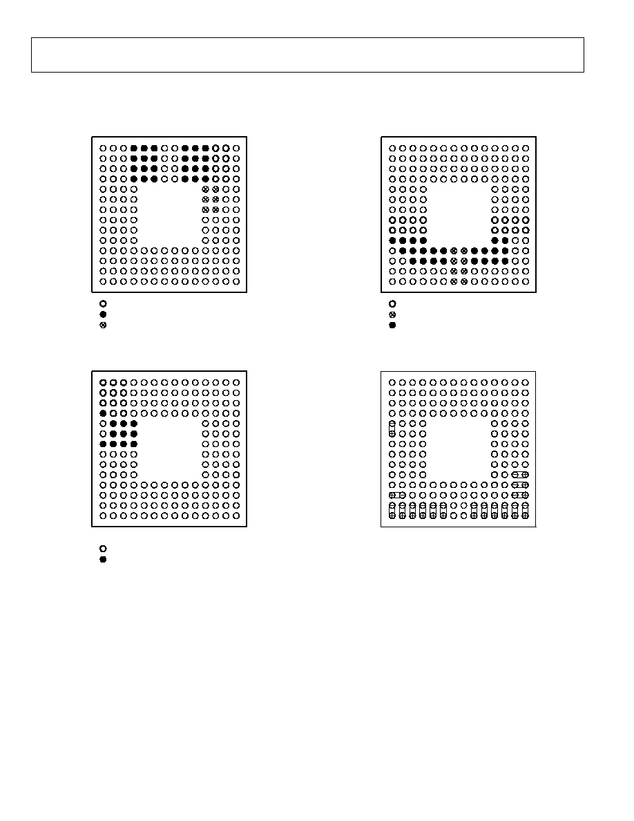
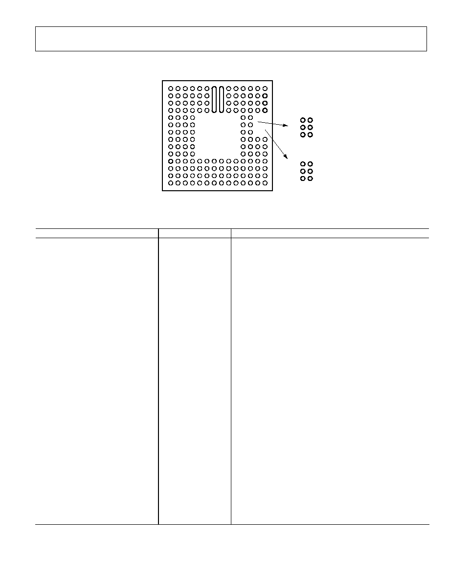
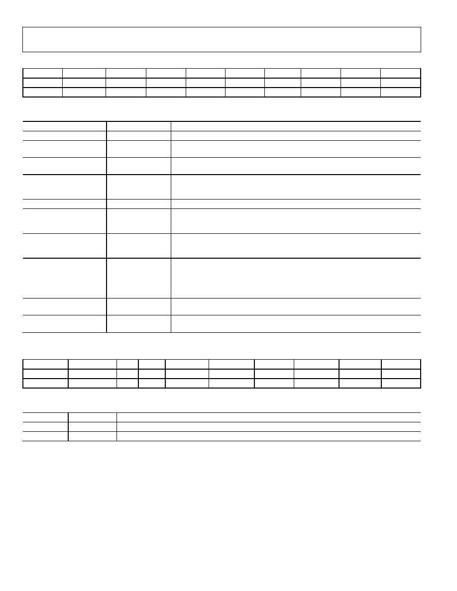
PIN CONFIGURATION AND FUNCTION DESCRIPTIONS
04862-002
A
B
C
D
E
F
G
H
J
K
L
M
N
P
14
13
12
11
10
8
7
6
3
2
1
9
5
4
AVSS, ANALOG SUPPLY GROUND
AVSS, ANALOG SUPPLY GROUND SHIELD
AVDD33, 3.3V, ANALOG SUPPLY
Figure 2. AD9736 Analog Supply Pins (Top View)
A
B
C
D
E
F
G
H
J
K
L
M
N
P
14
13
12
11
10
8
7
6
3
2
1
9
5
4
CVDD18, 1.8V CLOCK SUPPLY
CVSS, CLOCK SUPPLY GROUND
04862-003
Figure 3. AD9736 Clock Supply Pins (Top View)
A
B
C
D
E
F
G
H
J
K
L
M
N
P
14
13
12
11
10
8
7
6
3
2
1
9
5
4
04862-004
DVDD33, 3.3V DIGITAL SUPPLY
DVSS DIGITAL SUPPLY GROUND
DVDD18, 1.8V DIGITAL SUPPLY
Figure 4. AD9736 Digital Supply Pins (Top View)
A
B
C
D
E
F
CLK≠
CLK+
G
H
J
K
L
M
DB0 (LSB)
N
P
14
13
12
11
10
8
7
6
3
2
1
9
5
4
04862-005
DB1
DB1
0
DB11
DB12
DB13 (MSB)
DB9
DB8
DB7
DB6
DATACLK_
IN
DATACLK_
OUT
DB5
DB4
DB3
DB2
Figure 5. AD9736 Digital LVDS Inputs, Clock I/O (Top View)
AD9734/AD9735/AD9736
Rev. 0 | Page 11 of 68
A
B
C
D
E
F
G
H
J
K
L
M
N
P
14
13
12
11
10
8
7
6
3
2
1
9
5
4
04862-006
I120
VREF
IPTAT
PIN_MODE = 0,
SPI ENABLED
PIN_MODE = 1,
SPI DISABLED
PIN_MODE
UNSIGNED
2◊
FSC0
PD
FIFO
FSC1
IRQ
CSB
SCLK
RESET
SDIO
SDO
IOU
T
B
IOU
T
A
Figure 6. AD9736 Analog I/O and SPI Control Pins (Top View)
Table 5. Pin Function Descriptions
Pin No.
Mnemonic
Description
A1, A2, A3, B1, B2, B3, C1, C2, C3, D2, D3
CVDD18
1.8 V Clock Supply.
A4, A5, A6, A9, A10, A11, B4, B5, B6, B9,
B10, B11, C4, C5, C6, C9, C10, C11, D4, D5,
D6, D9, D10, D11
AVSS
Analog Supply Ground.
A7, B7, C7, D7
IOUTB
DAC Negative Output; 10 mA to 30 mA full-scale output current.
A8, B8, C8, D8
IOUTA
DAC Positive Output; 10 mA to 30 mA full-scale output current.
A12, A13, B12, B13, C12, C13, D12, D13
AVDD33
3.3 V Analog Supply.
A14
DNC
Do Not Connect.
B14
I120
Nominal 1.2 V Reference; tie to analog ground via 10 k resistor to
generate a 120 µA reference current.
C14
VREF
Band Gap Voltage Reference I/O; tie to analog ground via 1 nF
capacitor, output impedance approximately 5 k.
D1, E2, E3, E4, F2, F3, F4, G1, G2, G3, G4
CVSS
Clock Supply Ground.
D14
IPTAT
Factory Test Pin; output current proportional to absolute
temperature, approximately 10 µA at 25∞C with approximately
20 nA/∞C slope.
E1, F1
DACCLK-/DACCLK+
Negative/Positive DAC Clock Input (DACCLK).
E11, E12, F11, F12, G11, G12
AVSS
Analog Supply Ground Shield; tie to AVSS at the DAC.
E13
IRQ/UNSIGNED
If PIN_MODE = 0, IRQ: Active low open-drain interrupt request
output, pull up to DVDD33 with 10 k resistor.
If PIN_MODE = 1, UNSIGNED: Digital input pin where 0 = twos
complement input data format, 1 = unsigned.
E14
RESET/PD
If PIN_MODE = 0, RESET: 1 resets the AD9736.
If PIN_MODE = 1, PD: 1 puts the AD9736 in the power-down state.
F13
CSB/2◊
See Serial Peripheral Interface and Pin Mode Operation sections for
pin description.
F14
SDIO/FIFO
See the Pin Mode Operation section for pin description.
G13
SCLK/FSC0
See the Pin Mode Operation section for pin description.
G14
SDO/FSC1
See the Pin Mode Operation section for pin description.
H1, H2, H3, H4, H11, H12, H13, H14, J1, J2,
J3, J4, J11, J12, J13, J14
DVDD18
1.8 V Digital Supply.
K1, K2, K3, K4, K11, K12, L2, L3, L4, L5, L6,
L9, L10, L11, L12, M3, M4, M5, M6, M9,
M10, M11, M12
DVSS
Digital Supply Ground.

AD9734/AD9735/AD9736
Rev. 0 | Page 12 of 68
Pin No.
Mnemonic
Description
K13, K14
DB<13>-/DB<13>+
Negative/Positive Data Input Bit 13 (MSB); reduced swing LVDS.
L1
PIN_MODE
0 = SPI Mode; SPI enabled.
1 = PIN Mode; SPI disabled, direct pin control.
L7, L8, M7, M8, N7, N8, P7, P8
DVDD33
3.3 V Digital Supply.
L13, L14
DB<12>-/DB<12>+
Negative/Positive Data Input Bit 12; reduced swing LVDS.
M2, M1
DB<0>-/DB<0>+
Negative/Positive Data Input Bit 0 (LSB); reduced swing LVDS.
M13, M14
DB<11>-/DB<11>+
Negative/Positive Data Input Bit 11; reduced swing LVDS.
N1, P1
DB<1>-/DB<1>+
Negative/Positive Data Input Bit 1; reduced swing LVDS.
N2, P2
DB<2>-/DB<2>+
Negative/Positive Data Input Bit 2; reduced swing LVDS.
N3, P3
DB<3>-/DB<3>+
Negative/Positive Data Input Bit 3; reduced swing LVDS.
N4, P4
DB<4>-/DB<4>+
Negative/Positive Data Input Bit 4; reduced swing LVDS..
N5, P5
DB<5>-/DB<5>+
Negative/Positive Data Input Bit 5; reduced swing LVDS.
N6, P6
DATACLK_OUT-/
DATACLK_OUT+
Negative/Positive Data Output Clock; reduced swing LVDS.
N9, P9
DATACLK_IN-/
DATACLK_IN+
Negative/Positive Data Input Clock; reduced swing LVDS
N10, P10
DB<6>-/DB<6>+
Negative/Positive Data Input Bit 6; reduced swing LVDS.
N11, P11
DB<7>-/DB<7>+
Negative/Positive Data Input Bit 7; reduced swing LVDS.
N12, P12
DB<8>-/DB<8>+
Negative/Positive Data Input Bit 8; reduced swing LVDS.
N13, P13
DB<9>-/DB<9>+
Negative/Positive Data Input Bit 9; reduced swing LVDS.
N14, P14
DB<10>-/DB<10>+
Negative/Positive Data Input Bit 10; reduced swing LVDS.

AD9734/AD9735/AD9736
Rev. 0 | Page 13 of 68
TERMINOLOGY
Linearity Error (Integral Nonlinearity or INL)
The maximum deviation of the actual analog output from the
ideal output, determined by a straight line drawn from zero to
full scale.
Differential Nonlinearity (DNL)
The measure of the variation in analog value, normalized to full
scale, associated with a 1 LSB change in digital input code.
Monotonicity
A DAC is monotonic if the output either increases or remains
constant as the digital input increases.
Offset Error
The deviation of the output current from the ideal of zero is
called the offset error. For IOUTA, 0 mA output is expected
when the inputs are all 0s. For IOUTB, 0 mA output is expected
when all inputs are set to 1s.
Gain Error
The difference between the actual and ideal output span. The
actual span is determined by the output when all inputs are set
to 1s minus the output when all inputs are set to 0s.
Output Compliance Range
The range of allowable voltage at the output of a current output
DAC. Operation beyond the maximum compliance limits may
cause either output stage saturation or breakdown, resulting in
nonlinear performance.
Temperature Drift
Specified as the maximum change from the ambient (25∞C)
value to the value at either T
MIN
or T
MAX
. For offset and gain
drift, the drift is reported in ppm of full-scale range (FSR)
per ∞C. For reference drift, the drift is reported in ppm per ∞C.
Power Supply Rejection
The maximum change in the full-scale output as the supplies
are varied from nominal to minimum and maximum specified
voltages.
Settling Time
The time required for the output to reach and remain within a
specified error band about its final value, measured from the
start of the output transition.
Glitch Impulse
Asymmetrical switching times in a DAC give rise to undesired
output transients that are quantified by a glitch impulse. It is
specified as the net area of the glitch in pV-s.
Spurious-Free Dynamic Range
The difference, in dB, between the rms amplitude of the output
signal and the peak spurious signal over the specified bandwidth.
Total Harmonic Distortion (THD)
THD is the ratio of the rms sum of the first six harmonic
components to the rms value of the measured input signal. It is
expressed as a percentage or in decibels (dB).
Multitone Power Ratio
The spurious-free dynamic range containing multiple carrier
tones of equal amplitude. It is measured as the difference
between the rms amplitude of a carrier tone to the peak
spurious signal in the region of a removed tone.
AD9734/AD9735/AD9736
Rev. 0 | Page 14 of 68
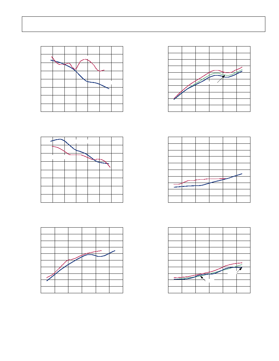
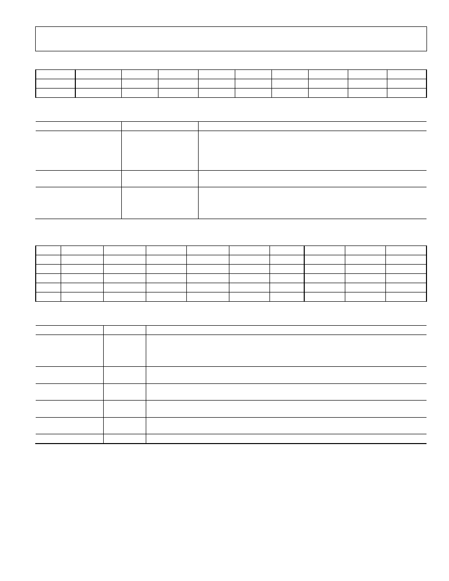
TYPICAL PERFORMANCE CHARACTERISTICS
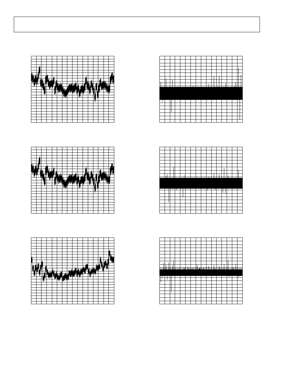
AD9736 STATIC LINEARITY, 10 mA FULL SCALE
04862-008
CODE
16384
0
2048
4096
6144
8192
10240 12288 14336
E
RROR (LS
B
)
1.00
0.75
0.50
0.25
0
≠0.25
≠0.50
≠0.75
≠1.00
≠1.25
≠1.50
≠1.75
≠2.00
Figure 7. AD9736 INL, -40∞C, 10 mA FS
04862-008
CODE
16384
0
2048
4096
6144
8192
10240 12288 14336
E
RROR (LS
B
)
1.00
0.75
0.50
0.25
0
≠0.25
≠0.50
≠0.75
≠1.00
≠1.25
≠1.50
≠1.75
≠2.00
Figure 8. AD9736 INL, 25∞C, 10 mA FS
04862-009
CODE
16384
0
2048
4096
6144
8192
10240 12288 14336
E
RROR (LS
B
)
1.00
0.75
0.50
0.25
0
≠0.25
≠0.50
≠0.75
≠1.00
≠1.25
≠1.50
≠1.75
≠2.00
Figure 9. AD9736 INL, 85∞C, 10 mA FS
04862-010
CODE
16384
0
2048
4096
6144
8192
10240 12288 14336
E
RROR (LS
B
)
1.0
0.8
0.6
0.4
0.2
0
≠0.2
≠0.4
≠0.6
≠0.8
≠1.0
Figure 10. AD9736 DNL, -40∞C, 10 mA FS
04862-011
CODE
16384
0
2048
4096
6144
8192
10240 12288 14336
E
RROR (LS
B
)
1.0
0.8
0.6
0.4
0.2
0
≠0.2
≠0.4
≠0.6
≠0.8
≠1.0
Figure 11. AD976 DNL, 25∞C, 10 mA FS
04862-012
CODE
16384
0
2048
4096
6144
8192
10240 12288 14336
E
RROR (LS
B
)
1.0
0.8
0.6
0.4
0.2
0
≠0.2
≠0.4
≠0.6
≠0.8
≠1.0
Figure 12. AD9736 DNL, 85∞C, 10 mA FS
AD9734/AD9735/AD9736
Rev. 0 | Page 15 of 68
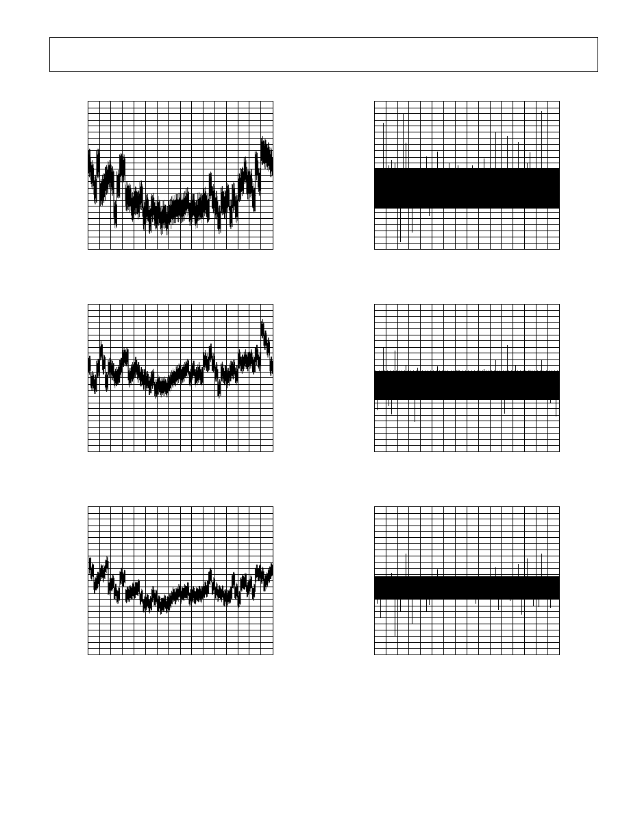
AD9736 STATIC LINEARITY, 20 mA FULL SCALE
04862-013
CODE
16384
0
2048
4096
6144
8192
10240 12288 14336
E
RROR (LS
B
)
1.0
0.8
0.6
0.4
0.2
0
≠0.2
≠0.4
≠0.6
≠0.8
≠1.0
≠1.2
≠1.4
Figure 13. AD9736 INL, -40∞C, 20 mA FS
04862-014
CODE
16384
0
2048
4096
6144
8192
10240 12288 14336
E
RROR (LS
B
)
1.0
0.8
0.6
0.4
0.2
0
≠0.2
≠0.4
≠0.6
≠0.8
≠1.0
≠1.2
≠1.4
Figure 14. AD9736 INL, 25∞C, 20 mA FS
04862-015
CODE
16384
0
2048
4096
6144
8192
10240 12288 14336
E
RROR (LS
B
)
1.0
0.8
0.6
0.4
0.2
0
≠0.2
≠0.4
≠0.6
≠0.8
≠1.0
≠1.2
≠1.4
Figure 15. AD9736 INL, 85∞C, 20 mA FS
04862-016
CODE
16384
0
2048
4096
6144
8192
10240 12288 14336
E
RROR (LS
B
)
0.6
0.5
0.4
0.3
0.2
0.1
0
≠0.1
≠0.2
≠0.3
≠0.4
≠0.5
≠0.6
Figure 16. AD9736 DNL, -40∞C, 20 mA FS
04862-017
CODE
16384
0
2048
4096
6144
8192
10240 12288 14336
E
RROR (LS
B
)
0.6
0.5
0.4
0.3
0.2
0.1
0
≠0.1
≠0.2
≠0.3
≠0.4
≠0.5
≠0.6
Figure 17. AD9736 DNL, 25∞C, 20 mA FS
04862-018
CODE
16384
0
2048
4096
6144
8192
10240 12288 14336
E
RROR (LS
B
)
0.6
0.5
0.4
0.3
0.2
0.1
0
≠0.1
≠0.2
≠0.3
≠0.4
≠0.5
≠0.6
Figure 18. AD9736 DNL, 85∞C, 20 mA FS
AD9734/AD9735/AD9736
Rev. 0 | Page 16 of 68
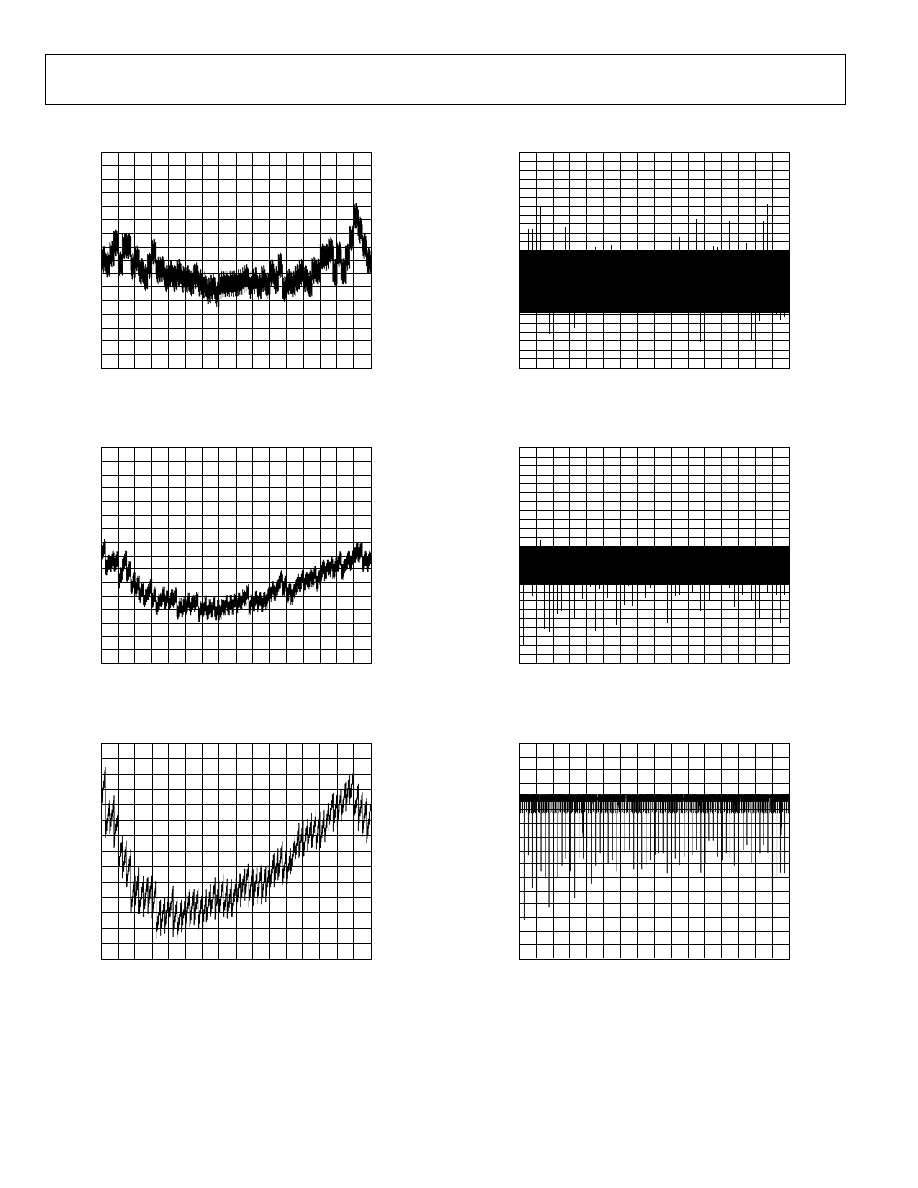
AD9736 STATIC LINEARITY, 30 mA FULL SCALE
04862-019
CODE
16384
0
2048
4096
6144
8192
10240 12288 14336
E
RROR (LS
B
)
2.0
1.5
1.0
0.5
0
≠0.5
≠1.0
≠1.5
≠2.0
Figure 19. AD9736 INL, -40∞C, 30 mA FS
04862-020
CODE
16384
0
2048
4096
6144
8192
10240 12288 14336
E
RROR (LS
B
)
2.0
1.5
1.0
0.5
0
≠0.5
≠1.0
≠1.5
≠2.0
Figure 20. AD9736 INL, 25∞C, 30 mA FS
04862-021
CODE
16384
0
2048
4096
6144
8192
10240 12288 14336
E
RROR (LS
B
)
2.0
1.5
1.0
0.5
0
0
0
0
≠0.5
≠0.5
≠1.0
≠1.0
≠1.5
≠1.5
≠2.0
Figure 21. AD9736 INL, 85∞C, 30 mA FS
04862-022
CODE
16384
0
2048
4096
6144
8192
10240 12288 14336
E
RROR (LS
B
)
0.6
0.3
0.4
0.5
0.2
0.1
0
≠0.1
≠0.2
≠0.3
≠0.4
≠0.5
≠0.6
Figure 22. AD9736 DNL, -40∞C, 30 mA FS
04862-023
CODE
16384
0
2048
4096
6144
8192
10240 12288 14336
E
RROR (LS
B
)
0.6
0.3
0.4
0.5
0.2
0.1
0
≠0.1
≠0.2
≠0.3
≠0.4
≠0.5
≠0.6
Figure 23. AD9736 DNL, 25∞C, 30 mA FS
04862-024
CODE
16384
0
2048
4096
6144
8192
10240 12288 14336
E
RROR (LS
B
)
1.0
0
0.5
≠0.5
≠1.0
≠1.5
≠2.0
≠2.5
≠3.0
Figure 24. AD9736 DNL, 85∞C, 30 mA FS
AD9734/AD9735/AD9736
Rev. 0 | Page 17 of 68
AD9735 STATIC LINEARITY, 10 mA, 20 mA, 30 mA FULL SCALE
04862-025
4095
0
2341
0.4
0.2
0.3
0.1
≠0.1
0
≠0.2
Figure 25. AD9735 INL, 25∞C, 10 mA FS
04862-026
4095
0
2341
0.15
≠0.20
≠0.15
≠0.10
≠0.05
0
0.05
0.10
Figure 26. AD9735 INL, 25∞C, 20 mA FS
04862-027
4095
0
2341
0.2
0
0.1
≠0.2
≠0.1
≠0.4
≠0.5
≠0.3
≠0.6
Figure 27. AD9735 INL, 25∞C, 30 mA FS
04862-028
4095
0
500
1000
1500
2000
2500
3000
3500
0.100
0.050
0
≠0.050
≠0.100
≠0.150
≠0.200
≠0.250
Figure 28. AD9735 DNL, 25∞C, 10 mA FS
04862-029
4095
0
500
1000
1500
2000
2500
3000
3500
0.100
0.075
0.025
0.050
0
≠0.025
≠0.075
≠0.050
≠0.100
≠0.125
Figure 29. AD9735 DNL, 25∞C, 20 mA FS
04862-030
4095
0
500
1000
1500
2000
2500
3000
3500
0.050
0
≠1.000
≠0.050
≠1.150
≠0.200
≠0.300
≠0.250
≠0.350
≠0.400
Figure 30. AD9735 DNL, 25∞C, 30 mA FS
AD9734/AD9735/AD9736
Rev. 0 | Page 18 of 68
AD9734 STATIC LINEARITY, 10 mA, 20 mA, 30 mA FULL SCALE
04862-031
1023
0
100
200
300
400
500
600
800
900
700
0.06
0.04
0.02
0
≠0.02
≠0.04
≠0.06
Figure 31. AD9734 INL, 25∞C, 10 mA FS
04862-032
1023
0
100
200
300
400
500
600
800
900
700
0.03
0.02
0.01
0
≠0.01
≠0.03
≠0.02
≠0.04
≠0.05
≠0.06
Figure 32. AD9734 INL, 25∞C, 20 mA FS
04862-033
1023
0
100
200
300
400
500
600
800
900
700
0.06
0.04
0.02
0
≠0.02
≠0.06
≠0.04
≠0.08
≠0.10
≠0.12
Figure 33. AD9734 INL, 25∞C, 30 mA FS
04862-034
1023
0
100
200
300
400
500
600
800
900
700
0.04
0.03
0.02
0.01
0
≠0.01
≠0.02
Figure 34. AD9734 DNL, 25∞C, 10 mA FS
04862-035
1023
0
100
200
300
400
500
600
800
900
700
0.03
0.02
0.01
0
≠0.01
≠0.02
≠0.03
Figure 35. AD9734 DNL, 25∞C, 20 mA FS
04862-036
1023
0
100
200
300
400
500
600
800
900
700
0.01
0
≠0.01
≠0.02
≠0.03
≠0.04
≠0.05
≠0.06
Figure 36. AD9734 DNL, 25∞C, 30 mA FS
AD9734/AD9735/AD9736
Rev. 0 | Page 19 of 68
AD9736 POWER CONSUMPTION, 20 mA FULL SCALE
04862-037
DVDD18
DVDD33
CVDD18
AVDD33
TOTAL
f
DAC
(MHz)
1500
0
250
500
750
1000
1250
POW
E
R
(
W
)
0.50
0.45
0.40
0.35
0.30
0.25
0.20
0.15
0.10
0.05
0
Figure 37. AD9736 1◊ Mode Power vs. f
DAC
at 25∞C
04862-038
f
DAC
(MHz)
1500
0
250
500
750
1000
1250
POW
E
R
(
W
)
0.7
0.6
0.5
0.4
0.3
0.2
0.1
0
DVDD18
DVDD33
VCDD18
AVDD33
TOTAL
Figure 38. AD9736, 2◊ Interpolation Mode Power vs. f
DAC
at 25∞C
AD9736 DYNAMIC PERFORMANCE, 20 mA FULL SCALE
04862-039
800MSPS
1GSPS
1.2GSPS
f
OUT
(MHz)
600
0
50
100 150 200 250 300 350 400 450 500 550
S
F
DR (dBc
)
80
75
70
65
60
55
50
Figure 39. AD9736 SFDR vs. f
OUT
over f
DAC
at 25∞C
04862-040
f
OUT
(MHz)
600
0
50
100 150 200 250 300 350 400 450 500 550
S
F
DR (dBc
)
80
75
70
65
60
55
50
+85∞C
+25∞C
≠40∞C
Figure 40. AD9736 SFDR vs. f
OUT
over Temperature
04862-041
550
0
50
100 150 200 250 300 350 400 450 500
76
78
72
74
70
68
66
64
62
60
56
54
58
52
f
OUT
(MHz)
S
F
DR (dBc
)
Figure 41. AD9736 SFDR vs. f
OUT
over 50 parts, 25∞C, 1.2 GSPS
04862-042
550
0
50
100 150 200 250 300 350 400 450 500
92
86
88
90
82
80
84
78
76
74
70
72
66
68
62
60
64
58
f
OUT
(MHz)
IMD (dBc
)
Figure 42. AD9736 IMD vs. f
OUT
over 50 parts, 25∞C,1.2 GSPS
AD9734/AD9735/AD9736
Rev. 0 | Page 20 of 68
04862-043
f
OUT
(MHz)
600
0
100
200
300
400
500
IMD (dBc
)
90
85
80
75
70
65
60
55
50
800MSPS
1GSPS
1.2GSPS
Figure 43. AD9736 IMD vs. f
OUT
over f
DAC
at 25∞C
04862-044
f
OUT
(MHz)
600
0
100
200
300
400
500
IMD (dBc
)
90
85
80
75
70
65
60
55
50
+85∞C
+25∞C
≠40∞C
Figure 44. AD9736 IMD vs. f
OUT
over Temperature, 1.2 GSPS
04862-045
f
OUT
(MHz)
100
0
10
IMD AND S
F
DR (dBc
)
95
90
85
80
75
70
65
60
55
IMD
SFDR
Figure 45. AD9736 Low Frequency IMD and SFDR vs. f
OUT
, 25∞C, 1.2 GSPS
04862-046
f
OUT
(MHz)
350
0
50
100
150
200
250
300
SFDR, IM
ID (
d
Bc)
90
85
80
75
70
65
60
55
50
THIRD-ORDER IMD
SFDR
Figure 46. AD9736 IMD and SFDR vs. f
OUT
, 25∞C, 1.2 GSPS, 2◊ Interpolation
04862-047
f
OUT
(MHz)
600
0
100
200
300
400
500
S
F
DR (dBc
)
80
75
70
65
60
55
50
45
40
0dBFS
≠6dBFS
≠12dBFS
Figure 47. AD9736 SFDR vs. f
OUT
over A
OUT
, 25∞C, 1.2 GSPS
04862-048
f
OUT
(MHz)
600
0
100
200
300
400
500
IMD (dBc
)
90
85
80
75
70
65
60
55
50
0dBFS
≠6dBFS
≠12dBFS
Figure 48. AD9736 IMD vs. f
OUT
over A
OUT
, 25∞C, 1.2 GSPS
AD9734/AD9735/AD9736
Rev. 0 | Page 21 of 68
AD9736 DYNAMIC PERFORMANCE, 20 mA FULL SCALE
04862-049
f
OUT
(MHz)
350
0
50
100
150
200
250
300
S
F
DR, IMD (dBc
)
90
85
80
75
70
65
60
55
50
SFDR_1◊
SFDR_2◊
Figure 49. AD9736 SFDR vs. f
OUT
, 25∞C, 1.2 GSPS, 1◊ and 2◊ Interpolation
04862-050
f
OUT
(MHz)
350
0
50
100
150
200
250
300
S
F
DR, IMD (dBc
)
90
85
80
75
70
65
60
55
50
THIRD-ORDER IMD_1◊
THIRD-ORDER IMD_2◊
Figure 50. AD9736 IMD vs. f
OUT
, 25∞C, 1.2 GSPS, 1◊ and 2◊ Interpolation
04862-051
f
OUT
(MHz)
600
0
100
200
300
400
500
NS
D (dBm/Hz)
≠150
≠154
≠156
≠152
≠158
≠160
≠162
≠164
≠166
≠168
≠170
1GSPS
1.2GSPS
Figure 51. AD9736 1-Tone NSD vs. f
OUT
over f
DAC
, 25∞C
04862-052
f
OUT
(MHz)
600
0
100
200
300
400
500
NS
D (dBm/Hz)
≠150
≠154
≠156
≠152
≠158
≠160
≠162
≠164
≠166
≠168
≠170
+85∞C
+25∞C
≠40∞C
Figure 52. AD9736 1-Tone NSD vs. f
OUT
over Temperature, 1.2 GSPS
04862-053
f
OUT
(MHz)
600
0
100
200
300
400
500
NS
D (dBm/Hz)
≠150
≠154
≠156
≠152
≠158
≠160
≠162
≠164
≠166
≠168
≠170
1GSPS
1.2GSPS
Figure 53. AD9736 8-Tone NSD vs. f
OUT
over f
DAC
, 25∞C
04862-054
f
OUT
(MHz)
600
0
100
200
300
400
500
NS
D (dBm/Hz)
≠150
≠154
≠156
≠152
≠158
≠160
≠162
≠164
≠166
≠168
≠170
+85∞C
+25∞C
≠40∞C
Figure 54. AD9736 8-Tone NSD vs. f
OUT
over Temperature, 1.2 GSPS
AD9734/AD9735/AD9736
Rev. 0 | Page 22 of 68
04862-055
550
0
50
100 150 200 250 300 350 400 450 500
≠159
≠158
≠160
≠157
≠161
≠162
≠163
≠164
≠165
≠166
f
OUT
(MHz)
NS
D (dBm/
H
z)
Figure 55. AD9736 1-Tone NSD vs. f
OUT
over 50 Parts, 1.2 GSPS, 25∞C
04862-056
550
0
50
100 150 200 250 300 350 400 450 500
≠162
≠163
≠161
≠164
≠165
≠166
≠167
f
OUT
(MHz)
NS
D (dBm/Hz)
Figure 56. AD9736 1-Tone NSD vs. f
OUT
over 50 Parts, 1.2 GSPS, 25∞C
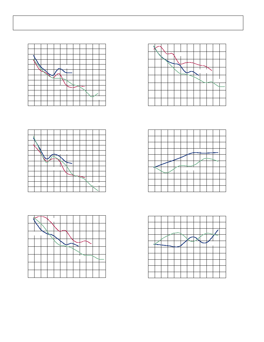
AD9736, AD9735, AD9734 WCDMA ACLR, 20 mA FULL SCALE
04862-057
#ATTEN 6dB
PAVG
10
W1
S2
CENTER 134.83MHz
#RES BW 30kHz
VBW 300kHz
SPAN 33.88MHz
SWEEP 109.9ms (601pts)
REF ≠22.75dBm
#AVG
LOG 10dB/
RMS RESULTS
OFFSET FREQ
REF BW
dBc
dBm
dBc
dBm
CARRIER POWER
5.00MHz
3.840MHz
≠81.65
≠92.37
≠81.39
≠92.11
≠10.72dBm/
10.0MHz
3.840MHz
≠82.06
≠92.78
≠82.43
≠93.16
3.84000MHz
15.0MHz
3.884MHz
≠82.11
≠92.83
≠82.39
≠93.11
LOWER
UPPER
Figure 57. AD9736 WCDMA Carrier at 134.83 MHz, f
DAC
= 491.52 MSPS

AD9734/AD9735/AD9736
Rev. 0 | Page 23 of 68
04862-058
RMS RESULTS
OFFSET FREQ
REF BW
dBc
dBm
dBc
dBm
CARRIER POWER
5.00MHz
3.840MHz
≠80.32
≠91.10
≠80.60
≠91.38
≠10.72dBm/
10.0MHz
3.840MHz
≠81.13
≠91.91
≠80.75
≠91.53
3.84000MHz
15.0MHz
3.884MHz
≠80.43
≠91.21
≠81.36
≠92.13
LOWER
UPPER
PAVG
10 S2
CENTER 134.83MHz
#RES BW 30kHz
VBW 300kHz
#ATTEN 6dB
SPAN 33.88MHz
SWEEP 109.9ms (601pts)
REF ≠22.75dBm
#AVG
LOG 10dB/
Figure 58. AD9735 WCDMA Carrier at 134.83 MHz, f
DAC
= 491.52 MSPS
04862-059
RMS RESULTS
OFFSET FREQ
REF BW
dBc
dBm
dBc
dBm
CARRIER POWER
5.00MHz
3.840MHz
≠71.07
≠81.83
≠71.23
≠81.99
≠10.76dBm/
10.0MHz
3.840MHz
≠70.55
≠81.31
≠71.42
≠82.19
3.84000MHz
15.0MHz
3.884MHz
≠70.79
≠81.56
≠71.25
≠82.01
LOWER
UPPER
PAVG
10 S2
CENTER 134.83MHz
#RES BW 30kHz
VBW 300kHz
#ATTEN 6dB
SPAN 33.88MHz
SWEEP 109.9ms (601pts)
REF ≠22.75dBm
#AVG
LOG 10dB/
Figure 59. AD9734 WCDMA Carrier at 134.83 MHz, f
DAC
= 491.52 MSPS
AD9734/AD9735/AD9736
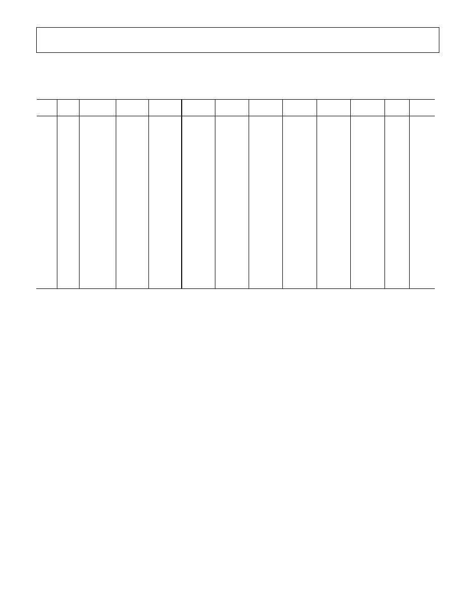
Rev. 0 | Page 24 of 68
AD9735, AD9734 DYNAMIC PERFORMANCE, 20 mA FULL SCALE
04862-060
f
OUT
(MHz)
600
0
50
100 150 200 250 300 350 400 450 500 550
S
F
DR (dBc
)
80
75
70
65
60
55
50
800MSPS
1GSPS
1.2GSPS
Figure 60. AD9735 SFDR vs. f
OUT
over f
DAC
, 1.2 GSPS
04862-061
f
OUT
(MHz)
600
0
50
100 150 200 250 300 350 400 450 500 550
S
F
DR (dBc
)
80
75
70
65
60
55
50
800MSPS
1GSPS
1.2GSPS
Figure 61. AD9734 SFDR vs. f
OUT
over f
DAC
, 1.2 GSPS
04862-062
f
OUT
(MHz)
600
0
50
100 150 200 250 300 350 400 450 500 550
IMD (dBc
)
90
85
80
75
70
65
60
55
50
800MSPS
1GSPS
1.2GSPS
Figure 62. AD9735 IMD vs. f
OUT
over f
DAC
, 1.2 GSPS
04862-063
f
OUT
(MHz)
600
0
50
100 150 200 250 300 350 400 450 500 550
IMD (dBc
)
90
85
80
75
70
65
60
55
50
800MSPS
1GSPS
1.2GSPS
Figure 63. AD9734 IMD vs. f
OUT
over f
DAC
, 1.2 GSPS
04862-064
f
OUT
(MHz)
600
0
50
100 150 200 250 300 350 400 450 500 550
NS
D (dBc
/Hz)
≠150
≠152
≠154
≠156
≠158
≠160
≠162
≠164
≠166
≠168
≠170
1 TONE
8 TONES
Figure 64. AD9735 NSD vs. f
OUT
, 1.2 GSPS
04862-065
f
OUT
(MHz)
600
0
50 100 150 200 250 300 350 400 450 500 550
NS
D (dBc
/
H
z)
≠149
≠147
≠145
≠151
≠153
≠155
≠157
≠159
≠161
≠163
≠165
1 TONE
8 TONES
Figure 65. AD9734 NSD vs. f
OUT
, 1.2 GSPS
AD9734/AD9735/AD9736
Rev. 0 | Page 25 of 68
SPI REGISTER MAP
Write 0 to unspecified or reserved bit locations. Reading these bits returns unknown values.
Table 6. SPI Register Map
ADR
Dec
ADR
Hex
Register
Name
Bit 7
Bit 6
Bit 5
Bit 4
Bit 3
Bit 2
Bit 1
Bit 0
Default
Hex
Pin Mode
Hex
0
00
MODE
SDIO_DIR
LSBFIRST
RESET
LONG_INS
2X MODE
FIFO MODE
DATAFRMT
PD
00
00
1
01
IRQ
LVDS
SYNC
CROSS
RESV'D
IE_LVDS
IE_SYNC
IE_CROSS
RESV'D
00
00
2
02
FSC_1
SLEEP
FSC<9>
FSC<8>
02
02
3
03
FSC_2
FSC<7>
FSC<6>
FSC<5>
FSC<4>
FSC<3>
FSC<2>
FSC<1>
FSC<0>
00
00
4
04
LVDS_CNT1
MSD<3>
MSD<2>
MSD<1>
MSD<0>
MHD<3>
MHD<2>
MHD<1>
MHD<0>
00
00
5
05
LVDS_CNT2
SD<3>
SD<2>
SD<1>
SD<0>
LCHANGE
ERR_HI
ERR_LO
CHECK
00
00
6
06
LVDS_CNT3
LSURV
LAUTO
LFLT<3>
LFLT<2>
LFLT<1>
LFLT<0>
LTRH<1>
LTRH<0>
00
00
7
07
SYNC_CNT1
FIFOSTAT3
FIFOSTAT2
FIFOSTAT1
FIFOSTAT0
VALID
SCHANGE
PHOF<1>
PHOF<0>
00
00
8
08
SYNC_CNT2
SSURV
SAUTO
SFLT<3>
SFLT<2>
SFLT<1>
SFLT<0>
RESV'D
STRH<0>
00
00
9
09
RESERVED
10
0A
CROS_CNT1
UPDEL<5>
UPDEL<4>
UPDEL<3>
UPDEL<2>
UPDEL<1>
UPDEL<0>
00
00
11
0B
CROS_CNT2
DNDEL<5>
DNDEL<4>
DNDEL<3>
DNDEL<2>
DNDEL<1>
DNDEL<0>
00
00
12
0C
RESERVED
13
0D
RESERVED
14
0E
ANA_CNT1
MSEL<1>
MSEL<0>
TRMBG<2>
TRMBG<1>
TRMBG<0>
C0
C0
15
0F
ANA_CNT2
HDRM<7>
HDRM<6>
HDRM<5>
HDRM<4>
HDRM<3>
HDRM<2>
HDRM<1>
HDRM<0>
CA
CA
16
10
RESERVED
17
11
BIST_CNT
SEL<1>
SEL<0>
SIG_READ
LVDS_EN
SYNC_EN
CLEAR
00
00
18
12
BIST<7:0>
19
13
BIST<15:8>
20
14
BIST<23:16>
21
15
BIST<31:24>
22
16
CCLK_DIV
RESV'D
RESV'D
RESV'D
RESV'D
CCD<3>
CCD<2>
CCD<1>
CCD<0>
00
00

AD9734/AD9735/AD9736
Rev. 0 | Page 26 of 68
SPI REGISTER DESCRIPTIONS
Reading these registers returns previously written values for all defined register bits, unless otherwise noted. Reset value for write registers
in bold text.
MODE REGISTER (REG 00)
ADR
Name
Bit 7
Bit 6
Bit 5
Bit 4
Bit 3
Bit 2
Bit 1
Bit 0
0x00
MODE
SDIO_DIR
LSB/MSB
RESET
LONG_INS
2◊ MODE
FIFO MODE
DATAFRMT
PD
Table 7. MODE Register Bit Descriptions
Bit Name
Read/Write
Description
SDIO_DIR
: WRITE ->
0, Input only per SPI standard
1, Bidirectional per SPI standard
LSBFIRST
: WRITE ->
0, MSB first per SPI standard
1, LSB first per SPI standard
NOTE: Only change LSB/MSB order in single-byte instructions to avoid erratic behavior due to bit order
errors.
RESET
: WRITE->
0, Execute software reset of SPI and controllers, reload default register values except registers 0x00 and
0x04
1, Set software reset, write 0 on the next (or any following) cycle to release the reset
LONG_INS
: WRITE ->
0, Short (single-byte) instruction word
1, Long (two-byte) instruction word, not necessary since the maximum internal address is REG31 (0x1F)
2◊_MODE
: WRITE ->
0, Disable 2◊ interpolation filter
1, Enable 2◊ interpolation filter
FIFO_MODE
: WRITE ->
0, Disable FIFO synchronization
1, Enable FIFO synchronization
DATAFRMT
: WRITE ->
0, Signed input DATA with midscale = 0x0000
1, Unsigned input DATA with midscale = 0x2000
PD
: WRITE ->
0, Enable LVDS Receiver, DAC, and clock circuitry
1, Power down LVDS Receiver, DAC, and clock circuitry
INTERRUPT REQUEST REGISTER (IRQ) (REG 01)
ADR
Name
Bit 7
Bit 6
Bit 5
Bit 4
Bit 3
Bit 2
Bit 1
Bit 0
0x01
IRQ
LVDS
SYNC
CROSS
RESV'D
IE_LVDS
IE_SYNC
IE_CROSS
RESV'D
Table 8. Interrupt Register Bit Descriptions
Bit Name
Read/Write
Description
LVDS
: WRITE ->
Don't Care
: READ ->
0, No active LVDS receiver interrupt
1, Interrupt in LVDS receiver occurred
SYNC
: WRITE ->
Don't Care
: READ ->
0, No active SYNC logic interrupt
1, Interrupt in SYNC logic occurred
CROSS
: WRITE ->
Don't Care
: READ ->
0, No active CROSS logic interrupt
1, Interrupt in CROSS logic occurred
IE_LVDS
: WRITE ->
0, Reset LVDS receiver interrupt and disable future LVDS receiver interrupts
1, Enable LVDS receiver interrupt to activate IRQ pin
IE_SYNC
: WRITE ->
0, Reset SYNC logic interrupt and disable future SYNC logic interrupts
1, Enable SYNC logic interrupt to activate IRQ pin
IE_CROSS :
WRITE ->
0, Reset CROSS logic interrupt and disable future CROSS logic interrupts
1, Enable CROSS logic interrupt to activate IRQ pin
AD9734/AD9735/AD9736
Rev. 0 | Page 27 of 68
FULL SCALE CURRENT (FSC) REGISTER (REGS 02, 03)
ADR
Name
Bit 7
Bit 6
Bit 5
Bit 4
Bit 3
Bit 2
Bit 1
Bit 0
0x02
FSC_1
SLEEP
FSC<9>
FSC<8>
0x03
FSC_2
FSC<7> FSC<6>
FSC<5>
FSC<4>
FSC<3>
FSC<2>
FSC<1>
FSC<0>
Table 9. Full Scale Output Register Bit Descriptions
Bit Name
Read/Write
Description
SLEEP
: WRITE ->
0, Enable DAC output
1, Set DAC output current to 0 mA
FSC<9:0>
: WRITE ->
0x000, 10 mA full-scale output current
0x200, 20 mA full-scale output current
0x3FF, 30 mA full-scale output current
LVDS CONTROLLER (LVDS_CNT) REGISTER (REGS 04, 05, 06)
ADR
Name
Bit 7
Bit 6
Bit 5
Bit 4
Bit 3
Bit 2
Bit 1
Bit 0
0x04
LVDS_CNT1
MSD<3>
MSD<2>
MSD<1>
MSD<0>
MHD<3>
MHD<2>
MHD<1>
MHD<0>
0x05
LVDS_CNT2
SD<3>
SD<2>
SD<1>
SD<0>
LCHANGE
ERR_HI
ERR_LO
CHECK
0x06
LVDS_CNT3
LSURV
LAUTO
LFLT<3>
LFLT<2>
LFLT<1>
LFLT<0>
LTRH<1>
LTRH<0>
Table 10. LVDS Controller Register Bit Descriptions
Bit Name
Read/Write
Description
MSD<3:0>
: WRITE ->
0x0, Set setup delay for the measurement system
: READ ->
If ( LAUTO = 1) the latest measured value for the setup delay
If ( LAUTO = 0) read back of the last SPI write to this bit
MHD<3:0>
: WRITE ->
0x0, Set hold delay for the measurement system
: READ ->
If ( LAUTO = 1) the latest measured value for the hold delay
If ( LAUTO = 0) read back of the last SPI write to this bit
SD<3:0>
: WRITE->
0x0, Set sample delay
: READ ->
If ( LAUTO = 1) the result of a measurement cycle is stored in this register
If ( LAUTO = 0) read back of the last SPI write to this bit
LCHANGE
: READ ->
0, No change from previous measurement
1, Change in value from the previous measurement
NOTE: The average filter and the threshold detection are not applied to this bit
ERR_HI
: READ ->
One of the 15 LVDS inputs is above the input voltage limits of the IEEE reduce link specification.
ERR_LO
: READ ->
One of the 15 LVDS inputs is below the input voltage limits of the IEEE reduced link specification.
CHECK
: READ ->
0, Phase measurement--sampling in the previous or following DATA cycle
1, Phase measurement--sampling in the correct DATA cycle
LSURV
: WRITE ->
0, The controller stops after completion of the current measurement cycle
1, Continuous measurements are taken and an interrupt is issued if the clock alignment drifts beyond the
threshold value
LAUTO :
WRITE ->
0, Sample delay is not automatically updated
1, Continuously starts measurement cycles and updates the sample delay according to the measurement
NOTE: LSURV (Reg 06, Bit 7) must be set to 1 and the LVDS IRQ (Reg 01 Bit 3) must be set to 0 for AUTO mode
LFLT<3:0>
: WRITE ->
0x0, Average filter length, Delay = Delay + Delta Delay / 2^ LFLT<3:0>, values greater than 12 (0x0C) are
clipped to 12
LTRH<2:0> : : WRITE ->
000, Set auto update threshold values
AD9734/AD9735/AD9736
Rev. 0 | Page 28 of 68
SYNC CONTROLLER (SYNC_CNT) REGISTER (REGS 07, 08)
ADR
Name
Bit 7
Bit 6
Bit 5
Bit 4
Bit 3
Bit 2
Bit 1
Bit 0
0x07
SYNC_CNT1
FIFOSTAT3
FIFOSTAT2
FIFOSTAT1 FIFOSTAT0 VALID
SCHANGE
PHOF<1>
PHOF<0>
0x08
SYNC_CNT2
SSURV
SAUTO
SFLT<3>
SFLT<2>
SFLT<1>
SFLT<0>
RESV'D
STRH<0>
Table 11. SYNC Controller Register Bit Descriptions
Bit Name
Read/Write
Description
FIFOSTAT<2:0>
: READ ->
Position of FIFO read counter, range from 0 to 7
FIFOSTAT<3>
: READ ->
0, SYNC logic OK
1, Error in SYNC logic
VALID
: READ ->
0, FIFOSTAT<3:0> is not valid yet
1, FIFOSTAT<3:0> is valid after a reset
SCHANGE
: READ ->
0, No change in FIFOSTAT<3:0>
1, FIFOSTAT<3:0> has changed since the previous measurement cycle when SSURV =
1 (surveillance mode active)
PHOF<1:0>
: WRITE ->
00, Change the readout counter
: READ ->
Current setting of the readout counter (PHOF<1:0>) in surveillance mode (SSURV = 1)
after an interrupt
Current calculated optimal readout counter value in AUTO mode (SAUTO = 1)
SSURV :
WRITE ->
0, The controller stops after completion of the current measurement cycle
1, Continuous measurements are taken and an interrupt is issued if the readout
counter drifts beyond the threshold value
SAUTO
: WRITE ->
0, Readout counter (PHOF<3:0>) is not automatically updated
1, Continuously starts measurement cycles and updates the readout counter
according to the measurement
NOTE: SSURV (Reg 08 Bit 7) must be set to 1 and the SYNC IRQ (Reg 01 Bit 2) must be
set to 0 for AUTO mode
SFLT<3:0>
: WRITE ->
0x0, Average filter length, FIFOSTAT = FIFOSTAT + Delta FIFOSTAT/2 ^ SFLT<3:0>,
values greater than 12 (0x0C) are clipped to 12
STRH<0>
: WRITE ->
0, If FIFOSTAT<2:0> = 0 | 7, generate a SYNC interrupt
1, If FIFOSTAT<2:0> = 0 | 1 | 6 | 7, generate a SYNC interrupt
CROSS CONTROLLER (CROS_CNT) REGISTER (REGS 10, 11)
ADR
Name
Bit 7 Bit 6
Bit 5
Bit 4
Bit 3
Bit 2
Bit 1
Bit 0
0x0A
CROS_CNT1
≠
≠
UPDEL<5>
UPDEL<4> UPDEL<3>
UPDEL<2>
UPDEL<1>
UPDEL<0>
0x0B
CROS_CNT2
≠
≠
DNDEL<5>
DNDEL<4> DNDEL<3>
DNDEL<2>
DNDEL<1>
DNDEL<0>
Table 12. Cross Controller Register Description
Bit Name
Read/Write
Description
UPDEL<5:0>
: WRITE ->
0x00, Move the differential output stage switching point up, set to 0 if DNDEL is non-zero
DNDEL<5:0>
: WRITE ->
0x00, Move the differential output stage switching point down, set to 0 if UPDEL is non-zero
AD9734/AD9735/AD9736
Rev. 0 | Page 29 of 68
ANALOG CONTROL (ANA_CNT) REGISTER (REGS 14, 15)
ADR
Name
Bit 7
Bit 6
Bit 5
Bit 4
Bit 3
Bit 2
Bit 1
Bit 0
0x0E
ANA_CNT1
MSEL<1>
MSEL<0>
≠ ≠ ≠
TRMBG<2>
TRMBG<1> TRMBG<0>
0x0F
ANA_CNT2
HDRM<7> HDRM<6>
HDRM<5>
HDRM<4>
HDRM<3>
HDRM<2>
HDRM<1>
HDRM<0>
Table 13. Analog Control Register Bit Descriptions
Bit Name
Read/Write
Description
MSEL<1:0>
: WRITE ->
00, Mirror roll off frequency control = bypass
01, Mirror roll off frequency control = narrowest bandwidth
10, Mirror roll off frequency control = medium bandwidth
11, Mirror roll off frequency control = widest bandwidth
NOTE: See plot in the Analog Control Registers section.
TRMBG<2:0>
: WRITE ->
000, Band gap temperature characteristic trim
NOTE: See the plot in the Analog Control Registers section.
HDRM<7:0>
: WRITE ->
0xCA, Output stack headroom control
HDRM<7:4> set reference offset from AVDD33 (VCAS centering)
HDRM<3:0> set overdrive (current density) trim (temperature tracking)
Note: Set to 0xCA for optimum performance
BUILT-IN SELF TEST CONTROL (BIST_CNT) REGISTERS (REGS 17, 18, 19, 20, 21)
ADR
Name
Bit 7
Bit 6
Bit 5
Bit 4
Bit 3
Bit 2
Bit 1
Bit 0
0x11
BIST_CNT
SEL<1>
SEL<0>
SIG_READ
LVDS_EN
SYNC_EN
CLEAR
0x12
BIST<7:0>
BIST<7>
BIST<6>
BIST<5>
BIST<4>
BIST<3>
BIST<2>
BIST<1>
BIST<0>
0x13
BIST<15:8>
BIST<15>
BIST<14>
BIST<13>
BIST<12>
BIST<11>
BIST<10>
BIST<9>
BIST<8>
0x14
BIST<23:16> BIST<23>
BIST<22>
BIST<21>
BIST<20>
BIST<19>
BIST<18>
BIST<17>
BIST<16>
0x15
BIST<31:24> BIST<31>
BIST<30>
BIST<29>
BIST<28>
BIST<27>
BIST<26>
BIST<25>
BIST<24>
Table 14. BIST Register Bit Descriptions
Bit Name
Read/Write
Description
SEL<1:0>
: WRITE ->
00, Write result of the LVDS Phase 1 BIST to BIST<31:0>
01, Write result of the LVDS Phase 2 BIST to BIST<31:0>
10, Write result of the SYNC Phase 1 BIST to BIST<31:0>
11, Write result of the SYNC Phase 2 BIST to BIST<31:0>
SIG_READ
: WRITE ->
0, No action
1, Enable BIST signature readback
LVDS_EN WRITE->
0, No action
1, Enable LVDS BIST
SYNC_EN
: WRITE ->
0, No action
1, Enable SYNC BIST
CLEAR
: WRITE ->
0, No action
1, Clear all BIST registers
BIST<31:0>
: READ ->
Results of the built-in self test
AD9734/AD9735/AD9736
Rev. 0 | Page 30 of 68
CONTROLLER CLOCK PREDIVIDER (CCLK_DIV) READING REGISTER (REG 22)
ADR
Name
Bit 7
Bit 6
Bit 5
Bit 4
Bit 3
Bit 2
Bit 1
Bit 0
0x16
CCLK_DIV
RESV'D
RESV'D
RESV'D
RESV'D
CCD<3> CCD<2> CCD<1>
CCD<0>
Table 15. Clock Predivider Register Bit Descriptions
Bit Name
Read/Write
Description
CCD<3:0>
: WRITE ->
0x0, Controller clock = DACCLK/16
0x1, Controller clock = DACCLK/32
0x2, Controller clock = DACCLK/64 ...
0xF, Controller clock = DACCLK/524288
NOTE: The 100 MHz to 1.2 GHz DACCLK must be divided to less than 10 MHz for correct operation.
CCD<3:0> must be programmed to divide the DACCLK so that this relationship is not violated.
Controller Clock = DACCLK/(2 ^ ( CCD<3:0> + 4 ))

AD9734/AD9735/AD9736
Rev. 0 | Page 31 of 68
THEORY OF OPERATION
The AD9736, AD9735, and AD9734 are 14-, 12-, and 10-bit
DACs that run at an update rate up to 1.2 GSPS. Input data can
be accepted up to the full 1.2 GSPS rate, or a 2◊ interpolation
filter may be enabled (2◊ mode) allowing full speed operation
with a 600 MSPS input data rate. DATA and DATACLK_IN
inputs are parallel LVDS, meeting the IEEE reduced swing
LVDS specifications with the exception of input hysteresis. The
DATACLK_IN input runs at one-half the input DATA rate in a
double data rate (DDR) format. Each edge of DATACLK_IN is
used to transfer DATA into the AD9736, as shown in Figure 77.
The DACCLK-/DACCLK+ inputs (Pins E1, F1) directly
drive the DAC core to minimize clock jitter. The DACCLK
signal is also divided by 2 (1◊ and 2◊ mode), then output as the
DATACLK_OUT. The DATACLK_OUT signal is used to clock
the data source. The DAC expects DDR LVDS data (DB<13:0>)
aligned with the DDR input clock (DATACLK_IN) from a
circuit similar to the one shown in Figure 94. Table 16 shows
the clock relationships.
Table 16. AD973x Clock Relationship
MODE DACCLK DATACLK_OUT DATACLK_IN
DATA
1◊
1.2 GHz
600 MHz
600 MHz
1.2 GSPS
2◊
1.2 GHz
600 MHz
300 MHz
600 MSPS
Maintaining correct alignment of data and clock is a common
challenge with high speed DACs, complicated by changes in
temperature and other operating conditions. Use of the
DATACLK_OUT signal to generate the data allows most of the
internal process, temperature, and voltage delay variation to be
cancelled. The AD973x further simplifies this high speed data
capture problem with two adaptive closed-loop timing
controllers.
One timing controller manages the LVDS data and data clock
alignment (LVDS controller), and the other manages the LVDS
data and DACCLK alignment (SYNC controller). The LVDS
controller locates the data transitions and delays the
DATACLK_IN so that its transition is in the center of the valid
data window. The SYNC controller manages the FIFO that
moves data from the LVDS DATACLK_IN domain to the
DACCLK domain. Both controllers can be operated in manual
mode under external processor control, surveillance mode
where error conditions generate external interrupts, or
automatic mode where errors are automatically corrected.
The LVDS and SYNC controllers include moving average
filtering for noise immunity and variable thresholds to control
their activity. Normally the controllers can be set to run in
automatic mode, and they make any necessary adjustments
without dropping or duplicating samples sent to the DAC. Both
controllers require initial calibration prior to entering automatic
update mode.
The AD973x analog output changes 35 DACCLK cycles after
the input data changes in 1◊ mode with the FIFO disabled. The
FIFO can add up to eight additional cycles of delay. This delay
can be read from the SPI port. Internal clock delay variation is
less than a single DACCLK cycle at 1.2 GHz (833 ps).
Stopping the AD973x DATACLK_IN while the DACCLK is still
running can lead to unpredictable output signals. This occurs
because the internal digital signal path is interleaved. The last
two samples clocked into the DAC continue to be clocked out
by DACCLK even after DATACLK_IN has been stopped. The
resulting output signal is at a frequency of one-half f
DAC,
and
the amplitude depends on the difference between the last two
samples.
Control of the AD973x functions is via the serially programmed
registers listed in Table 6. Optionally, a limited number of
functions may be directly set by external pins in pin mode.
AD9734/AD9735/AD9736
Rev. 0 | Page 32 of 68
SERIAL PERIPHERAL INTERFACE
The AD973x serial port is a flexible, synchronous serial
communications port, allowing easy interface to many
industry-standard microcontrollers and microprocessors. The
serial I/O is compatible with most synchronous transfer
formats, including both the Motorola SPIÆ and IntelÆ SSR
protocols. The interface allows read/write access to all registers
that configure the AD973x. Single- or multiple-byte transfers
are supported, as well as most significant bit first (MSB-first) or
least significant bit first (LSB-first) transfer formats. The
AD973x serial interface port can be configured as a single pin
I/O (SDIO) or two unidirectional pins for in/out (SDIO/SDO).
SDO (PIN G14)
SDIO (PIN F14)
SCLK (PIN G13)
CSB (PIN F13)
AD9736
SPI PORT
04862-066
Figure 66. AD973x SPI Port
The AD973x can optionally be configured via external pins
rather than the serial interface. When the PIN_MODE input
(Pin L1) is high, the serial interface is disabled and its pins are
reassigned for direct control of the DAC. Specific functionality
is described in the Pin Mode Operation section.
GENERAL OPERATION OF THE SERIAL INTERFACE
There are two phases to a communication cycle with the
AD973x. Phase 1 is the instruction cycle, which is the writing of
an instruction byte into the AD973x, coincident with the first
eight SCLK rising edges. The instruction byte provides the
AD973x serial port controller with information regarding the
data transfer cycle, which is Phase 2 of the communication
cycle. The Phase 1 instruction byte defines whether the
upcoming data transfer is read or write, the number of bytes in
the data transfer, and the starting register address for the first
byte of the data transfer. The first eight SCLK rising edges of
each communication cycle are used to write the instruction byte
into the AD973x.
The remaining SCLK edges are for Phase 2 of the communica-
tion cycle. Phase 2 is the actual data transfer between the
AD973x and the system controller. Phase 2 of the communica-
tion cycle is a transfer of 1, 2, 3, or 4 data bytes as determined
by the instruction byte. Using one multibyte transfer is the
preferred method. Single-byte data transfers are useful to
reduce CPU overhead when register access requires one byte
only. Registers change immediately upon writing to the last bit
of each transfer byte.
CSB (Chip Select) can be raised after each sequence of 8 bits
(except the last byte) to stall the bus. The serial transfer resumes
when CSB is lowered. Stalling on nonbyte boundaries resets the
SPI.
SHORT INSTRUCTION MODE (8-BIT INSTRUCTION)
The short instruction byte is shown in Table 17.
Table 17. SPI Instruction Byte
MSB
LSB
I7
I6
I5
I4
I3
I2
I1
I0
R/W
N1
N0
A4
A3
A2
A1
A0
R/W, Bit 7 of the instruction byte, determines whether a read or
a write data transfer occurs after the instruction byte write.
Logic high indicates read operation. Logic 0 indicates a write
operation. N1, N0, Bits 6 and 5 of the instruction byte,
determine the number of bytes to be transferred during the data
transfer cycle. The bit decodes are shown in Table 18.
A4, A3, A2, A1, A0, Bits 4, 3, 2, 1, 0 of the instruction byte,
determine which register is accessed during the data transfer
portion of the communications cycle. For multibyte transfers,
this address is the starting byte address. The remaining register
addresses are generated by the AD973x, based on the LSBFIRST
bit (Reg 00, Bit 6).
Table 18. Byte Transfer Count
N1
N2
Description
0
0
Transfer 1 byte
0
1
Transfer 2 bytes
1
0
Transfer 3 bytes
1
1
Transfer 4 bytes
LONG INSTRUCTION MODE (16-BIT INSTRUCTION)
The long instruction bytes are shown in Table 19.
Table 19. SPI Instruction Byte
MSB
LSB
I15
I14
I13
I12
I11
I10
I9
I8
R/W
N1
N0
A12
A11
A10
A9
A8
I7
I6
I5
I4
I3
I2
I1
I0
A7
A6
A5
A4
A3
A2
A1
A0
If LONG_INS = 1 (Reg 00, Bit 4), the instruction byte is
extended to 2 bytes where the second byte provides an
additional 8 bits of address information. Addresses 0x00 to 0x1F
are equivalent in short and long instruction modes. The
AD973x does not use any addresses greater than 31 (0x1F), so
always set LONG_INS = 0.
SERIAL INTERFACE PORT PIN DESCRIPTIONS
SCLK--Serial Clock.
The serial clock pin is used to
synchronize data to and from the AD973x and to run the
internal state machines. The maximum frequency of SCLK is
20 MHz. All data input to the AD973x is registered on the rising
edge of SCLK. All data is driven out of the AD973x on the
rising edge of SCLK.
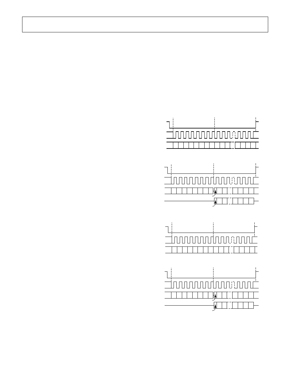
AD9734/AD9735/AD9736
Rev. 0 | Page 33 of 68
CSB--Chip Select.
Active low input starts and gates a
communication cycle. It allows more than one device to be used
on the same serial communications lines. The SDO and SDIO
pins goes to a high impedance state when this input is high.
Chip select should stay low during the entire communication
cycle.
SDIO--Serial Data I/O.
Data is always written into the
AD973x on this pin. However, this pin can be used as a bidirec-
tional data line. The configuration of this pin is controlled by
SDIO_DIR at Reg 00, Bit 7. The default is Logic 0, which
configures the SDIO pin as unidirectional.
SDO--Serial Data Out.
Data is read from this pin for protocols
that use separate lines for transmitting and receiving data. In
the case where the AD973x operates in a single bidirectional
I/O mode, this pin does not output data and is set to a high
impedance state.
MSB/LSB TRANSFERS
The AD973x serial port can support both MSB-first or LSB-first
data formats. This functionality is controlled by LSBFIRST at
Reg 00, Bit 6. The default is MSB first (LSBFIRST = 0).
When LSBFIRST = 0 (MSB first), the instruction and data bytes
must be written from the most significant bit to the least
significant bit. Multibyte data transfers in MSB-first format start
with an instruction byte that includes the register address of the
most significant data byte. Subsequent data bytes should follow
in order from high address to low address. In MSB-first mode,
the serial port internal byte address generator decrements for
each data byte of the multibyte communication cycle.
When LSBFIRST = 1 (LSB first), the instruction and data bytes
must be written from least significant bit to most significant bit.
Multibyte data transfers in LSB-first format start with an
instruction byte that includes the register address of the least
significant data byte followed by multiple data bytes. The serial
port internal byte address generator increments for each byte of
the multibyte communication cycle.
The AD973x serial port controller data address decrements
from the data address written toward 0x00 for multibyte I/O
operations if the MSB-first mode is active. The serial port
controller address increments from the data address written
toward 0x1F for multibyte I/O operations if the LSB-first mode
is active.
NOTES ON SERIAL PORT OPERATION
The AD973x serial port configuration is controlled by Reg 00,
Bits 4, 5, 6, and 7. Note that the configuration changes
immediately upon writing to the last bit of the register. For
multibyte transfers, writing to this register may occur during
the middle of communication cycle. Care must be taken to
compensate for this new configuration for the remaining bytes
of the current communication cycle. The same considerations
apply to setting the software reset, RESET (Reg 00, Bit 5). All
registers are set to their default values except Reg 00 and Reg 04
which remain unchanged.
Use of only single-byte transfers when changing serial port
configurations or initiating a software reset is highly
recommended. In the event of unexpected programming
sequences, the AD973x SPI may become inaccessible. For
example, if user code inadvertently changes the LONG_INS bit
or the LSBFIRST bit, the following bits may have unexpected
results. The SPI can be returned to a known state by writing an
incomplete byte (1 to 7 bits) of all 0s followed by 3 bytes of
0x00. This returns to MSB-first short instructions (Reg 00 =
0x00) so the device may be reinitialized.
R/W N1 N0 A4 A3 A2 A1 A0 D7
N
D6
N
D5
N
D0
0
D1
0
D2
0
D3
0
INSTRUCTION CYCLE
DATA TRANSFER CYCLE
CSB
SCLK
SDIO
04862-067
Figure 67. Serial Register Interface Timing, MSB-First Write
R/W N1 N0 A4 A3
A2 A1 A0
D7
D6
N
D5
N
D0
0
D1
0
D2
0
D3
0
D6
N
D5
N
D0
0
D1
0
D2
0
D3
0
INSTRUCTION CYCLE
DATA TRANSFER CYCLE
CSB
SCLK
SDIO
SDO
04862-068
D7
Figure 68. Serial Register Interface Timing, MSB-First Read
A0 A1 A2 A3 A4 N0 N1 R/W D0
0
D1
0
D2
0
D7
N
D6
N
D5
N
D4
N
INSTRUCTION CYCLE
DATA TRANSFER CYCLE
CSB
SCLK
SDIO
04862-069
Figure 69. Serial Register Interface Timing, LSB-First Write
INSTRUCTION CYCLE
DATA TRANSFER CYCLE
CSB
SCLK
SDIO
SDO
A0 A1 A2 A3 A4 N0 N1 R/W
D1
0
D2
0
D7
N
D6
N
D5
N
D4
N
D1
0
D2
0
D7
N
D6
N
D5
N
D4
N
04862-070
D0
D0
Figure 70. Serial Register Interface Timing, LSB-First Read
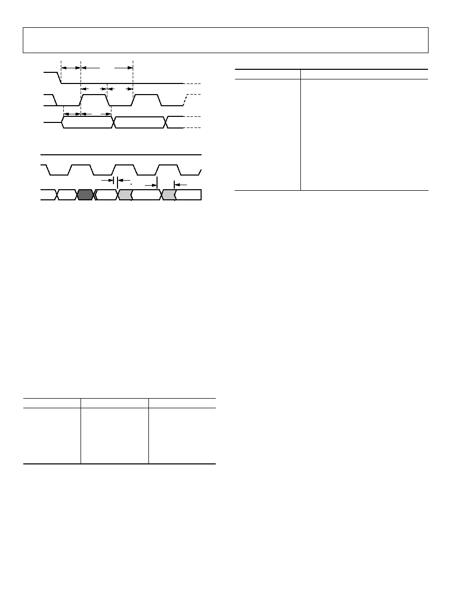
AD9734/AD9735/AD9736
Rev. 0 | Page 34 of 68
INSTRUCTION BIT 6
INSTRUCTION BIT 7
CSB
SCLK
SDIO
t
DS
t
DS
t
DH
t
PWH
t
PWL
t
SCLK
04862-071
Figure 71. Timing Diagram for SPI Register Write
I1
I0
D7
D6
D5
t
DV
t
DNV
CSB
SCLK
SDIO
04862-072
Figure 72. Timing Diagram for SPI Register Read
After the last instruction bit is written to the SDIO pin, the
driving signal must be set to a high impedance in time for the
bus to turn around. The serial output data from the AD973x is
enabled by the falling edge of SCLK. This causes the first output
data bit to be shorter than the remaining data bits, as shown in
Figure 72.
To assure proper reading of data, read the SDIO or SDO pin
prior to changing the SCLK from low to high.
Due to the more complex multibyte protocol, multiple AD973x
devices cannot be daisy-chained on the SPI bus. Multiple DACs
should be controlled by independent CSB signals.
PIN MODE OPERATION
When the PIN_MODE input (Pin L1) is set high, the SPI port is
disabled. The SPI port pins are remapped, as shown in Table 20.
The function of these pins is described in Table 21. The
remaining PIN_MODE register settings are shown in Table 6.
Table 20. SPI_MODE vs. PIN_MODE Inputs
Pin No.
PIN_MODE = 0
PIN_MODE = 1
E13
IRQ
UNSIGNED
F13
CSB
2◊
G13
SCLK
FSC0
E14
RESET
PD
F14
SDIO
FIFO
G14
SDO
FSC1
Table 21. PIN_MODE Input Functions
Pin
Function
UNSIGNED
0, Twos complement input data format
1, Unsigned input data format
2◊
0, Interpolation disabled
1, Interpolation = 2◊ enabled
FSC1, FSC0
00, Sleep mode
01, 10 mA full-scale output current
10, 20 mA full-scale output current
11, 30 mA full-scale output current
PD
0, Chip enabled
1, Chip in power-down state
FIFO
0, Input FIFO disabled
1, Input FIFO enabled
Care must be taken when using PIN_MODE, because only
the control bits shown in Table 21 can be changed. If the
remaining register default values are not suitable for the desired
operation, PIN_MODE cannot be used. If the FIFO is enabled,
the controller clock must be less than 10 MHz. This limits the
DAC clock to 160 MHz.
RESET OPERATION
The RESET pin forces all SPI register contents to their default
values (see Table 6), which places the DAC in a known state.
The software reset bit forces all SPI register contents, except
Reg 00 and Reg 04, to their default values.
The internal reset signal is derived from a logical OR operation
on the RESET pin state and from the software reset state. This
internal reset signal drives all SPI registers to their default
values, except Reg 00 and Reg 04, which are unaffected. The
data registers are not affected by either reset.
The software reset is asserted by writing 1 to Reg 00, Bit 5. It
may be cleared on the next SPI write cycle or a later write cycle.
PROGRAMMING SEQUENCE
The AD973x registers should be programmed in this order:
1.
Hardware reset
2.
SPI port configuration changes, if necessary
3.
Input format, if unsigned
4.
Interpolation, if in 2◊ mode
5.
Calibrate and set the LVDS Controller
6.
Enable the FIFO
7.
Calibrate and set the sync controller
Steps 1 through 4 are required, while 5 through 7 are optional.
The LVDS controller can help assure proper data reception in
the DAC with changes in temperature and voltage. The SYNC
controller manages the FIFO to assure proper transfer of the
received data to the DAC core with changes in temperature and
voltage. The DAC is intended to operate with both controllers
active unless data and clock alignment is managed externally.
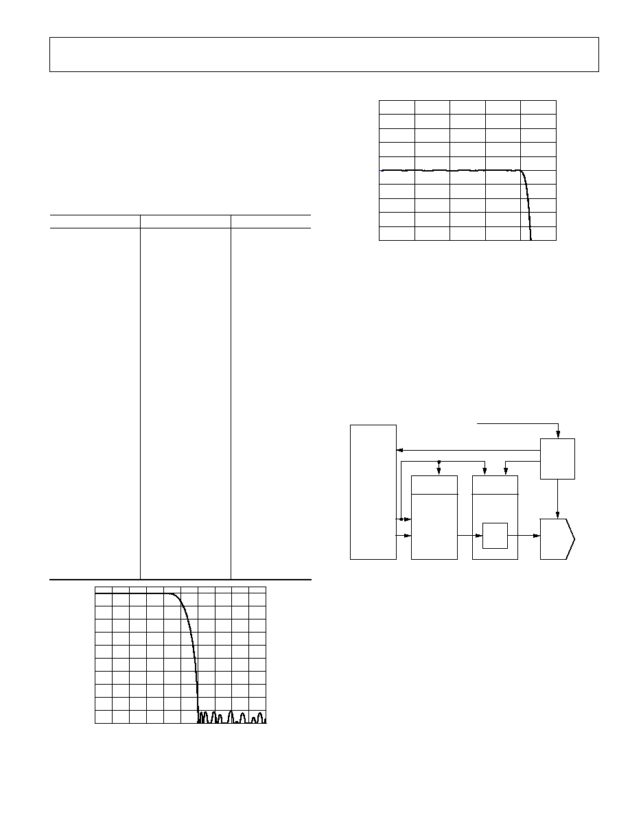
AD9734/AD9735/AD9736
Rev. 0 | Page 35 of 68
INTERPOLATION FILTER
In 2◊ mode, the input data is interpolated by a factor of 2 so it
aligns with the DAC update rate. The interpolation filter is a
hard-coded, 55-tap, symmetric FIR with a 0.001 dB pass-band
flatness and a stop-band attenuation of about 90 dB. The tran-
sition band runs from 20% of f
DAC
to 30% of f
DAC
. The FIR
response is shown in Figure 73 where the frequency axis is
normalized to f
DAC
Figure 74 shows the pass-band flatness and
Table 22 shows the 16-bit filter coefficients.
Table 22. FIR Interpolation Filter Coefficients
Coefficient No.
Coefficient No.
Tap Weight
h1
h55
-7
h2
h54
0
h3
h53
24
h4
h52
0
h5
h51
-62
h6
h50
0
h7
h49
135
h8
h48
0
h9
h47
-263
h10
h46
0
h11
h45
471
h12
h44
0
h13
h43
-793
h14
h42
0
h15
h41
1273
h16
h40
0
h17
h39
-1976
h18
h38
0
h19
h37
3012
h20
h36
0
h21
h35
-4603
h22
h34
0
h23
h33
7321
h24
h32
0
h25
h31
-13270
h26
h30
0
h27
h29
41505
h28
65536
04862-
073
FREQUENCY NORMALIZED TO
f
DAC
0.50
0
0.05 0.10 0.15 0.20 0.25 0.30 0.35 0.40 0.45
MAGNIT
UDE (d
B)
0
≠10
≠20
≠30
≠40
≠50
≠60
≠70
≠80
≠90
≠100
Figure 73. AD973x Interpolation Filter Response
04862-074
FREQUENCY NORMALIZED TO
f
DAC
0.25
0
0.10
0.05
0.15
0.20
M
A
G
N
IT
UDE (
d
B)
0.10
0.06
0.08
0.02
≠0.02
≠0.06
0.04
0
≠0.04
≠0.08
≠0.10
Figure 74. AD973x Interpolation Filter Pass-Band Flatness
DATA INTERFACE CONTROLLERS
There are two internal controllers that can be utilized in the
operation of the AD973x. The first controller helps maintain
optimum LVDS data sampling and the second controller helps
maintain optimum synchronization between the DACCLK and
the incoming data. The LVDS controller is responsible for
optimizing the sampling of the data from the LVDS bus
(DB13:0), while the SYNC controller resolves timing problems
between the DAC_CLK (CLK+, CLK-) and the DATACLK. A
block diagram of these controllers is shown in Figure 75.
DATACLK_OUT
DATACLK
DATACLK_IN
FIFO
DAC
LVDS
SAMPLE
LOGIC
CLK
CONTROL
LVDS
CONTROLLER
DB<13:0>
DATA
SOURCE
i.e., FPGA
SYNC
LOGIC
SYNC
CONTROLLER
04862-075
Figure 75. AD973x Data Controllers
The controllers are clocked with a divided-down version of the
DAC_CLK. The divide ratio is set utilizing the controller clock
predivider bits (CCD<3:0>) located at REG 22, Bits 3:0 to
generate the controller clock as follows:
Controller Clock = DAC_CLK/(2(CCD<3:0> + 4))
Note that the controller clock may not exceed 10 MHz for
correct operation. Until CCD<3:0> has been properly
programmed to meet this requirement, the DAC output may
not be stable. This means the FIFO cannot be enabled in
PIN_MODE unless the DACCLK is less than 160 MHz.
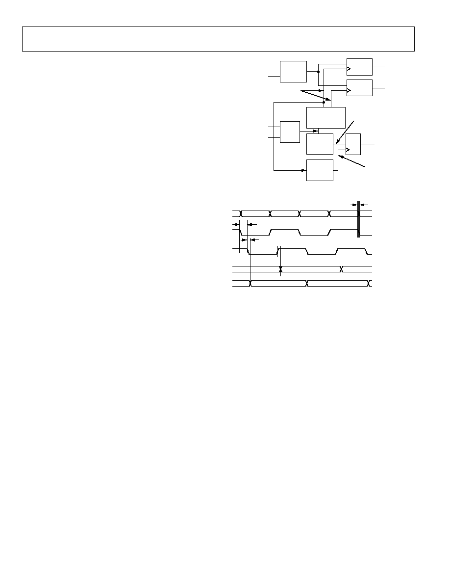
AD9734/AD9735/AD9736
Rev. 0 | Page 36 of 68
The LVDS and SYNC controllers can be independently
operated in three modes via SPI port Reg 06 and Reg 08:
∑
Manual mode
∑
Surveillance mode
∑
Auto mode
In manual mode, all of the timing measurements and updates
are externally controlled via the SPI.
In surveillance mode, each controller takes measurements and
calculates a new optimal value continuously. The result of the
measurement can be passed through an averaging filter before
evaluating the results for increased noise immunity. The filtered
result is compared to a threshold value set via Reg 06 and
Reg 08 of the SPI port. If the error is greater than the threshold,
an interrupt is triggered and the controller stops. Reg 01 of the
SPI port controls the interrupts with Bits 3 and 2 enabling the
respective interrupts and Bits 7 and 6 indicating the respective
controller's interrupt. If an interrupt is enabled, it also activates
the AD973x IRQ pin. In order to clear an interrupt, the
interrupt enable bit of the respective controller must be set to 0
for at least 1 controller clock cycle (controller clock <10 MHz).
Auto mode is almost identical to surveillance mode. Instead
of triggering an interrupt and stopping the controller, the
controller automatically updates its settings to the newly
calculated optimal value and continues to run.
LVDS SAMPLE LOGIC
A simplified diagram of the AD973x LVDS data sampling
engine is shown in Figure 76 and the timing diagram is shown
in Figure 77.
The incoming LVDS data is latched by the data sampling signal
(DSS), which is derived from DATACLK_IN. The LVDS
controller delays DATACLK_IN to create the data sampling
signal (DSS), which is adjusted to sample the LVDS data in the
center of the valid data window. The skew between the
DATACLK_IN and the LVDS data bits (DB<13:0>) must be
minimal for proper operation. Therefore, it is recommended
that the DATACLK_IN be generated in the same manner as the
LVDS data bits (DB<13:0>) with the same driver and data lines
(that is, it should just be another LVDS data bit running a
constant 01010101... sequence, as shown in Figure 94).
If the DATACLK_IN signal is stopped, the DACCLK continues
to generate an output signal based on the last two values
clocked into the registers that drive D1 and D2, as shown in
Figure 76. If these two registers are not equal, a large output at a
frequency of one-half f
DAC
may be generated at the DAC output.
DB<13:0>
DATACLK_IN
LVDS
RX
DELAYED
CLOCK
SIGNAL
CLOCK
SAMPLING
SIGNAL
CHECK
D1
D2
DATA SAMPLING
SIGNAL
LVDS
RX
MSD<3:0>
DELAY
MSD<3:0>
DELAY
FF
SD<3:0>
SAMPLE DELAY
FF
FF
04862-076
Figure 76. AD973x Internal LVDS Data Sampling Logic
SAMPLE
DELAY
PROP DELAY
TO LATCH
PROP DELAY
TO LATCH
CLK TO DB SKEW
DB13:0
D1
D2
DATACLK_IN
DATA SAMPLING
SIGNAL (DSS)
04862-
077
Figure 77. AD973x Internal LVDS Data Sampling Logic Timing
LVDS SAMPLE LOGIC CALIBRATION
The internal DSS delay must be calibrated to optimize the data
sample timing. Once calibrated, the AD973x can generate an
IRQ or automatically correct its timing if temperature or voltage
variations change the timing too much. This calibration is done
by using the delayed clock sampling signal (CSS) to sample the
delayed clock signal (DCS). The LVDS sampling logic can find
the edges of the DATACLK_IN signal and from this measure-
ment the center of the valid data window can be located.
The internal delay line that derives the delayed DSS from
DATACLK_IN is controlled by SD3:0 (Reg 05, Bits 7:4), while
the DCS is controlled by MSD3:0 (Reg 04, Bits 7:4), and the CSS
is controlled by MHD3:0 (Reg 04, Bits 3:0).
DATACLK_IN transitions must be time aligned with the LVDS
data (DB<13:0>) transitions. This allows the CSS, derived from
the DATACLK_IN, to find the valid data window of DB<13:0>
by locating the DATACLK_IN edges. The latching (rising) edge
of CSS is initially placed using Bits SD<3:0> and can then be
shifted to the left using MSD<3:0> and to the right using
MHD<3:0>. When CSS samples the DCS and the result is 1,
(which can be read back via the check bit at Reg 05, Bit 0) the
sampling is occurring in the correct data cycle. To find the
leading edge of the data cycle, increment the measured setup
delay until the check bit goes low. In order to find the trailing
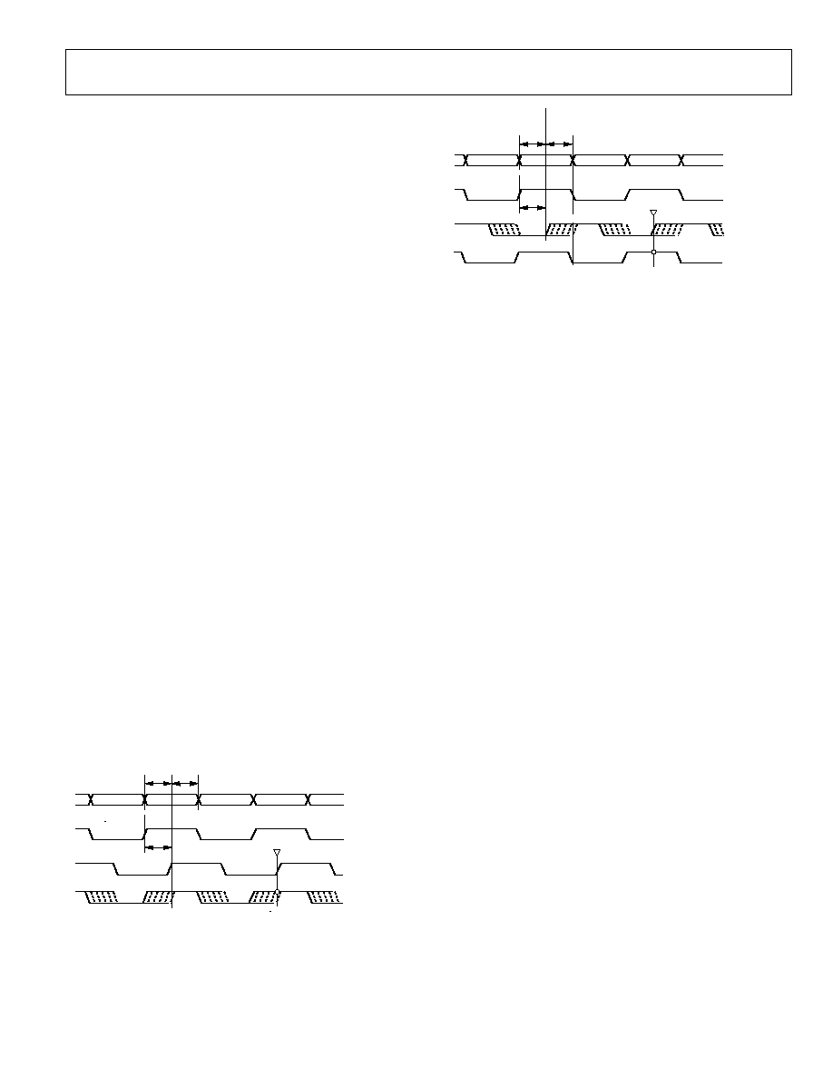
AD9734/AD9735/AD9736
Rev. 0 | Page 37 of 68
edge, increment the measured hold delay (MHD) until check
goes low. Always set MHD = 0 when incrementing MSD and
vice versa.
The incremental units of SD, MSD, and MHD are in units of real
time, not fractions of a clock cycle. The nominal step size is 80 ps.
OPERATING THE LVDS CONTROLLER IN
MANUAL MODE VIA THE SPI PORT
The manual operation of the LVDS controller allows the user to
step through both the setup and hold delays to calculate the
optimal sampling delay (that is, the center of the data eye).
With SD<3:0> and MHD<3:0> set to 0, increment the setup time
delay (MSD<3:0>, Reg 04, Bits 7:4) until the check bit (Reg 05,
Bit 0) goes low and record this value. This locates the leading
DATACLK_IN (and data) transition, as shown in Figure 78.
With SD<3:0> and MSD<3:0> set to 0, increment the hold time
delay (MHD<3:0>, Reg 04, Bits 3:0) until the check bit (Reg 05,
Bit 0) goes low and record this value. This locates the trailing
DATACLK_IN (and DB<13:0>) transition, as shown in Figure 79.
Once both DATACLK_IN edges are located, the sample delay
(SD<3:0>, Reg 05, Bits 7:4) must be updated according to the
following equation:
Sample Delay = (MHD - MSD)/2
After updating SD<3:0>, verify that the sampling signal is in the
middle of the valid data window by adjusting both MHD and
then MSD with the new sample delay until the check bit goes
low. The new MHD and MSD values should be equal to or
within one unit delay if SD<3:0> was set correctly.
MHD and MSD may not be equal to or within one unit delay if
the external clock jitter and noise exceeds the internal delay
resolution. Differences of 2, 3, or more are possible and may
require more filtering to provide stable operation.
The sample delay calibration should be performed prior to
enabling surveillance mode or auto mode.
SETUP TIME (
t
S
)
SAMPLE DELAY
MSD<3:0> = 0 1 2 3 4 5
CSS SAMPLE DCS
CHECK = 1
SD<3:0>
DB<13:0>
DATACLK_IN
CSS WITH
MHD<3:0> = 0
DSC DELAYED
BY MSD<3:0>
04862-
078
Figure 78. Setup Delay Measurement
SETUP TIME (
t
S
)
HOLD TIME (
t
H
)
SAMPLE DELAY
CSS SAMPLE DCS
CHECK = 1 1 1 1 1 0
CHECK = 1
SD<3:0>
0
4862-
079
MSD<3:0> = 0 1 2 3 4 5
DB<13:0>
DATACLK_IN
CSS WITH
MHD<3:0> = 0
DSC DELAYED
BY MSD<3:0> = 0
Figure 79. Hold Delay Measurement
OPERATING THE LVDS CONTROLLER IN
SURVEILLANCE AND AUTO MODE
In surveillance mode, the controller searches for the edges of
the data eye in the same manner as in the manual mode of
operation and triggers an interrupt if the clock sampling signal
(CSS) has moved more than the threshold value set by
LTHR<1:0> (Reg 06, Bits 1:0).
There is an internal filter that averages the setup and hold time
measurements to filter out noise and glitches on the clock lines.
Average Value = ( MHD ≠ MSD)/2
New Average = Average Value + ( Average/2 ^ LFLT<3:0> )
If an accumulating error in the average value causes it to exceed
the threshold value (LTHR<1:0>), an interrupt is issued.
The maximum allowable value for LFLT<3:0> is 12. If
LFLT<3:0> is too small, clock jitter and noise can cause erratic
behavior. In most cases, LFLT can be set to the maximum value.
In surveillance mode, the ideal sampling point should first be
found using manual mode and applied to the sample delay
registers. The user should then set the threshold and filter
values depending on how far the CSS signal is allowed to drift
before an interrupt occurs. Then set the surveillance bit high
(Reg 06, Bit 7) and monitor the interrupt signal either via the
SPI port read back (Reg 01, Bit 7) or the IRQ pin.
In auto mode, the same steps should be taken to set up the
sample delay, threshold, and filter length. To run the controller
in auto mode, both the LAUTO (Reg 06, Bit 6) and LSURV
(Reg 06, Bit 7) bits need to be set to 1. In auto mode, the LVDS
interrupt should be set low (Reg 01, Bit 3) to allow the sample
delay to be automatically updated if the threshold value is
exceeded.
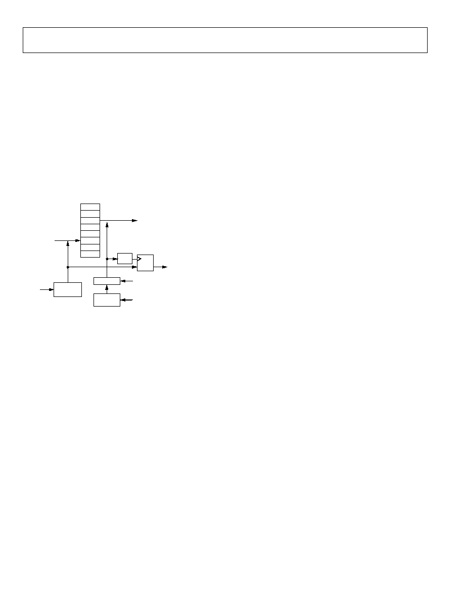
AD9734/AD9735/AD9736
Rev. 0 | Page 38 of 68
SYNC LOGIC AND CONTROLLER
A FIFO structure is utilized to synchronize the data transfer
between the DACCLK and the DATACLK_IN clock domains.
The sync controller writes data from DB<13:0> into an 8-word
memory register based on a cyclic write counter clocked by the
DSS, which is a delayed version of DACCLK_IN. The data is
read out of the memory based on a second cyclic read counter
clocked by DACCLK. The 8-word FIFO shown in Figure 80
provides sufficient margin to maintain proper timing under
most conditions. The sync logic is designed to prevent the read
and write pointers from crossing. If the timing drifts far enough
to require an update of the phase offset (PHOF<1:0>), two
samples are duplicated or dropped. Figure 81 shows the timing
diagram for the sync logic.
8 WORD
MEMORY
READ
COUNTER
PHOF<1:0>
DACCLK
FIFOSTAT<2:0>
DSS
M0
M7
ZD
DAC<13:0>
ADDER
WRITE
COUNTER
FF
DAC<13:0>
04862-080
Figure 80. Sync Logic Block Diagram
SYNC LOGIC AND CONTROLLER OPERATION
The relationship between the readout pointer and the write
pointer initially is unknown because the startup relationship
between DACCLK and DATACLK_IN is unknown. The sync
logic measures the relative phase between the two counters with
the zero detect block and the flip-flop in Figure 80. The relative
phase is returned in FIFOSTAT<2:0> (Reg 07, Bits 6:4), and
sync logic errors are indicated by FIFOSTAT<3> (Reg 07, Bit 7).
If FIFOSTAT<2:0> returns a value of 0 or 7, it signifies that the
memory is sampling in a critical state (read and write pointers
are close to crossing). If the FIFOSTAT<2:0> returns a value of
3 or 4, it signifies the memory is sampling at the optimal state
(read and write pointers are farthest apart). If FIFOSTAT<2:0>
returns a critical value, the pointer can be adjusted with the
phase offset PHOF<1:0> (Reg 07, Bits 1:0). Due to the
architecture of the FIFO, the phase offset can only adjust the
read pointer in steps of 2.
OPERATING IN MANUAL MODE
To start operating the DAC in manual mode, allow DACCLK
and DATACLK_IN to stabilize, then enable FIFO mode (Reg
00, Bit 2). Read FIFOSTAT<2:0> (Reg 07, Bits 6:4) to determine
if adjustment is needed. For example, if FIFOSTAT<2:0> = 6,
the timing is not yet critical but it is not optimal. To return to
an optimal state (FIFOSTAT<2:0> = 4), the PHOF<1:0>
(Reg 07, Bits 1:0) needs to be set to 1. Setting PHOF<1:0> = 1
effectively increments the read pointer by 2. This causes the
write pointer value to be captured two clocks later, decreasing
FIFOSTAT<2:0> from 6 to 4.
OPERATION IN SURVEILLANCE AND AUTO MODES
Once FIFOSTAT<2:0> has been manually placed in an optimal
state, the AD973x sync logic can be run in surveillance or auto
mode. To start, turn on surveillance mode by setting SSURV = 1
(Reg 08, Bit 7) then enable the sync interrupt (Reg 01, Bit 2). If
STRH<0> = 0 (Reg 08, Bit 0), an interrupt occurs if
FIFOSTAT<2:0> = 0 or 7. If STRH<0> = 1 (Reg 08, Bit 0), an
interrupt occurs if FIFOSTAT<2:0> = 0, 1, 6, or 7. The interrupt
can be read at Reg 01, Bit 6 at the AD973x IRQ pin.
To enter auto mode, complete the preceding steps then set
SAUTO = 1 (Reg 08, Bit 6). Next, set the SYNC interrupt = 0
(Reg 01, Bit 2), to allow the phase offset (PHOF<1:0>) to be
automatically updated if FIFOSTAT<2:0> violates the threshold
value. The FIFOSTAT signal is filtered to improve noise
immunity and reduce unnecessary phase offset updates. The
filter operates with the following algorithm:
FIFOSTAT = FIFOSTAT + FIFOSTAT/2 ^ SFLT<3:0>
where 0 SFLT<3:0> 12. Values greater than 12 are set to 12.
If SFLT<3:0> is too small, clock jitter and noise can cause
erratic behavior. Normally SFLT can be set to the maximum
value.
FIFO BYPASS
When the FIFO_MODE bit (Reg 01, Bit 2) is set to 0, the FIFO
is bypassed with a mux. When the FIFO is enabled, the pipeline
delay through the AD973x increases by the delta between the
FIFO read pointer and write pointer plus 4 more clock periods.
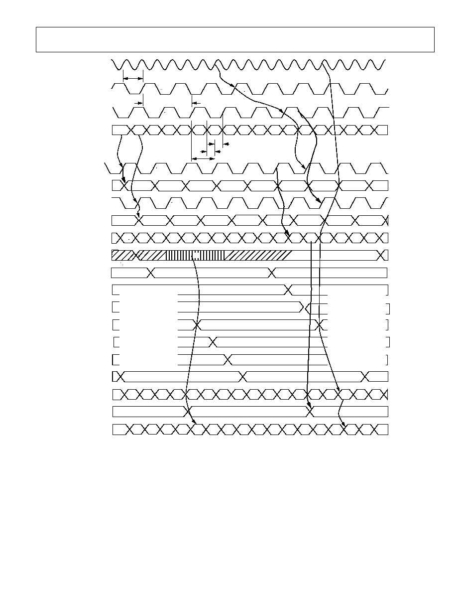
AD9734/AD9735/AD9736
Rev. 0 | Page 39 of 68
D
INTERNAL DELAY
DACCLK
DATACLK_OUT
DATACLK_IN
DATA_IN
A
A
B
B
0
1
2
3
4
5
6
7
0
1
2
3
4
5
6
7
0
4
5
6
7
0
1
2
3
4
1
2
3
4
5
6
7
0
C
C
D
D
E
E
F
F
G
G
H
H
I
I
J
J
K
K
L
L
M
A
B
C
D
E
F
G
H
I
J
K
L
M
M
N
N
I
A
O
O
Q
P
P
Q
R
DSS1
DSS2
D2
WRITE_PTR1
SAFE ZONE
DATA 'A' CAN BE
SAFELY READ FROM
THE FIFO IN THE
SAFE ZONE. IN THE
ERROR ZONE, THE
POINTERS MAY
BRIEFLY OVERLAP
DUE TO CLOCK JITTER
OR NOISE.
FIFOSTAT IS SET
EQUAL TO THE
WHITE POINTER
EACH TIME THE
READ POINTER
CHANGES FROM
7 TO 0.
ERROR ZONE
M0
M1
B
C
E
F
G
4
4
4
H
J
M2
M3
M4
M5
M6
M7
READ_PTR1
FIFOSTAT
DAC_DATA
D1
EXTERNAL DELAY
SAMPLE_HOLD
SAMPLE_SETUP
SAMPLE_DELAY
04862-081
Figure 81. SYNC Logic Timing Diagram
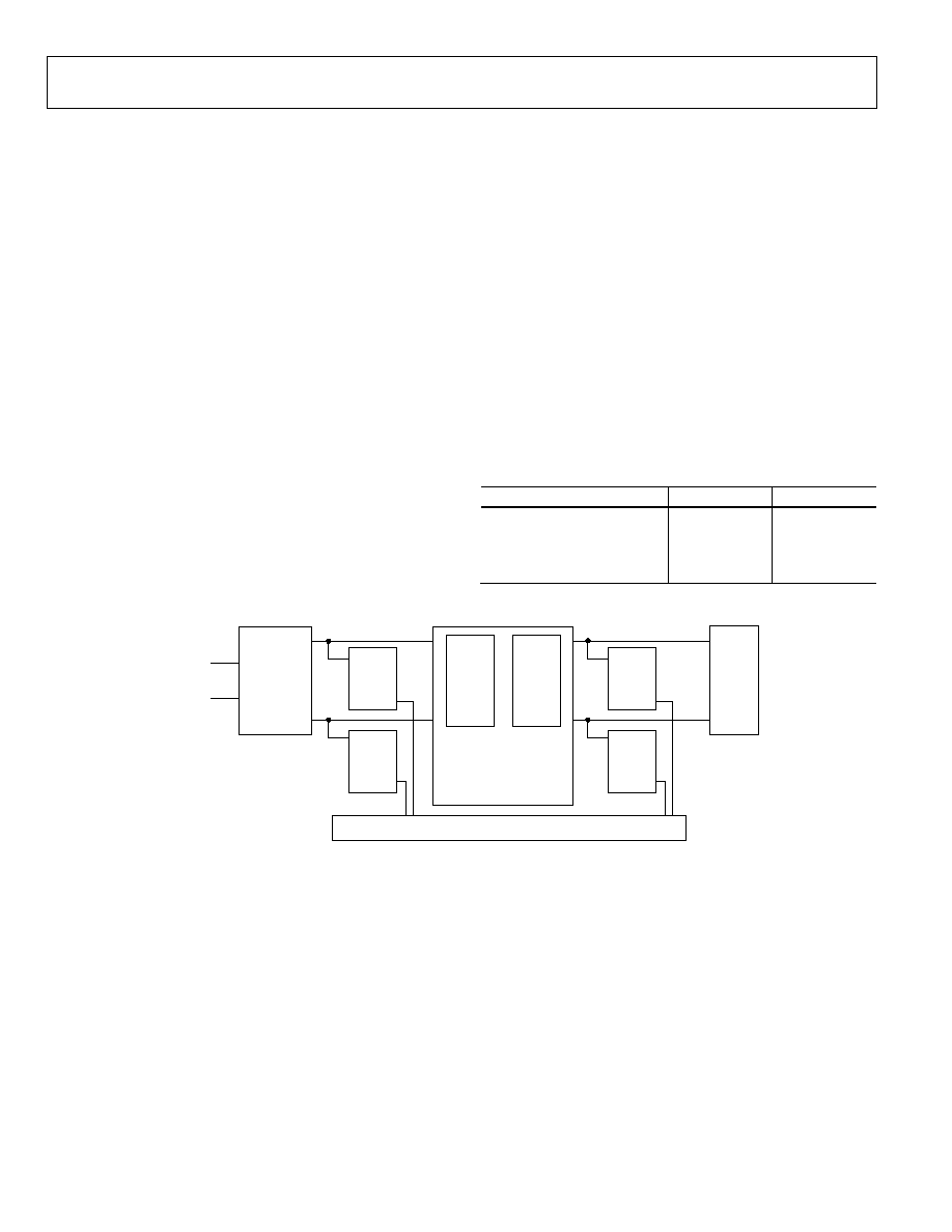
AD9734/AD9735/AD9736
Rev. 0 | Page 40 of 68
DIGITAL BUILT-IN SELF TEST (BIST)
OVERVIEW
The AD973x includes an internal signature generator that
processes incoming data to create unique signatures. These
signatures can be read back from the SPI port, allowing
verification of correct data transfer into the AD973x. BIST
vectors provided on the AD973x-EB evaluation board CD can
be used to check the full width data input or individual bits for
PCB debug, utilizing the procedure in the AD973x BIST
Procedure section. Alternatively, any vector may be used
provided the expected signature is calculated in advance. The
MATLABÆ routine in the Generating Expected Signatures
section may be used to calculate the expected signature. BIST
should be used to verify correct data transfer because not all
errors may be evident on a spectrum analyzer. There are four
BIST signature generators that can be read back using
Register 18 to Register 21, based on the setting of the BIST
selection bits (Reg 17, Bits 7:6), as shown in Table 23. The BIST
signature returned from the AD973x depends on the digital
input during the test. Because the filters in the DAC have
memory, it is important to put the correct idle value on the
DATA inputs to flush the memory prior to reading the BIST
signature.
Placing the idle value on the data inputs also allows the BIST to
be set up while the DAC clock is running. The idle value should
be all 0s in unsigned mode (0x0000) and all 0s except for the
MSB in twos complement mode (0x2000).
The BIST consists of two stages; the first stage is after the LVDS
receiver and the second stage is after the FIFO. The first BIST
stage verifies correct sampling of the data from the LVDS bus
while the second BIST stage verifies correct synchronization
between the DAC_CLK domain and the DATACLK_IN
domain. The BIST vector is generated using 32-bit LFSR
signature logic. Because the internal architecture is a 2-bus
parallel system, there are two 32-bit LFSR signature logic blocks
on the both the LVDS and sync blocks. Figure 82 shows where
the LVDS and sync phases are located.
Table 23. BIST Selection Bits
Bit
SEL<1>
SEL<0>
LVDS Phase 1
0
0
LVDS Phase 2
0
1
SYNC Phase 1
1
0
SYNC Phase 2
1
1
LVDS
RX
DB<13:0>
DATACLK_IN
SYNC LOGIC
FIFO
2x
D1
D2
DAC
LVDS
BIST
PH1
(RISE)
LVDS
BIST
PH2
(FALL)
SYNC
BIST
PH1
(RISE)
SYNC
BIST
PH2
(FALL)
SPI PORT
04862-082
Figure 82. Block Diagram Showing LVDS and Sync Phase 1 and Phase 2

AD9734/AD9735/AD9736
Rev. 0 | Page 41 of 68
AD973x BIST PROCEDURE
1.
Set RESET pin = 1.
2.
Set input DATA = 0x0000 for signed (0x2000 for
unsigned).
3.
Enable DATACLK_IN if it is not already running.
4.
Run for at least 16 DATACLK_IN cycles.
5.
Set RESET pin = 0.
6.
Run for at least 16 DATACLK_IN cycles.
7.
Set RESET pin = 1.
8.
Run for at least 16 DATACLK_IN cycles.
9.
Set RESET pin = 0.
10.
Set desired operating mode (1◊ mode and signed data are
default values and expected for the supplied BIST vectors).
11.
Set CLEAR (Reg 17, Bit 0), SYNC_EN (Reg 17, Bit 1) and
LVDS_EN (Reg 17, Bit 2) high.
12.
Wait 50 DATACLK_IN cycles to allow 0s to propagate
through and clear sync signatures.
13.
Set CLEAR low.
14.
Read all signature registers (REG 21, 20, 19, and 18) for
each of the four SEL (Reg 17, Bits 7:6) values and verify
they are all 0x00.
LVDS Phase 1
a.
Reg 17 set to 0x26 (SEL1 = 0, SEL0 = 0,
SIG_READ = 1, LVDS_EN = 1, SYNC_EN = 1).
b.
Read Registers 20, 19, 18, and 17.
LVDS Phase 2
a.
Reg 17 set to 0x66 (SEL1= 0, SEL0 = 1,
SIG_READ = 1, LVDS_EN = 1, SYNC_EN = 1).
b.
Read Registers 20, 19, 18, and 17.
SYNC Phase 1
a.
Reg 17 set to 0xA6 (SEL1= 1, SEL0 = 0,
SIG_READ = 1, LVDS_EN = 1, SYNC_EN = 1).
b.
Read Registers 20, 19, 18, and 17.
SYNC Phase 2
a.
Reg 17 set to 0xE6 (SEL1= 1, SEL0 = 1,
SIG_READ = 1, LVDS_EN = 1, SYNC_EN = 1).
b.
Read Registers 20, 19, 18, and 17.
15.
Clock the BIST vector into the AD973x.
16.
After the BIST vector has been clocked into the part, hold
DATA = 0x0000 for signed (0x2000 for unsigned);
otherwise, the additional nonzero data changes the
signature.
17.
Read all signature registers (Reg 21, 20, 19, and 18 as
described in Step 14 ) for each of the four SEL (Reg 17,
Bits 7:6) values, and verify that they match the expected
signatures shown in Table 24.
18.
In some cases, the BIST circuitry may not be completely
cleared, and an incorrect signature may be read. If this
occurs, loop back to Step 11 and rerun the test to obtain
the correct result. In an automated test, it may be best to
always run the vector twice to assure a correct result.
AD973x EXPECTED BIST SIGNATURES
The BIST vectors provided on the AD973x-EB CD are in signed
mode, so no programming needs to be done to the part to pass
the BIST. The BIST vector is for 1◊, no FIFO, and signed data.
For testing all 14 input bits, use the vector all_bits_unsnew.txt
and verify against the signatures in Table 24.
Table 24. Expected BIST Data Readback for All Bits
LVDS Phase 1
LVDS Phase 2
SYNC Phase 1
SYNC Phase 2
CF71487C 66DF5250 CF71487C 66DF5250
For individual bit tests, use the vectors named bitn.txt (where n
is the desired bit number being tested) and compare them
against the values in Table 25.
Table 25. Expected BIST Data Readback for Individual Bits
Vector
Bit No.
LVDS Rise
Expected
LVDS Fall
Expected
bit0.txt 0
AABF0A00
2A400500
bit1.txt 1
2BBF0A00
6B400500
bit2.txt 2
29BE0A00
E9400500
bit3.txt 3
2DBC0A00
ED410500
bit4.txt 4
25B80A00
E5430500
bit5.txt 5
35B00A00
F5470500
bit6.txt 6
15A00A00
D54F0500
bit7.txt 7
55800A00
955F0500
bit8.txt 8
D5C00A00
157F0500
bit9.txt 9
D5410A00
153E0500
bit10.txt 10
D5430B00
15BC0500
bit11.txt 11
D5470900
15B80400
bit12.txt 12
D54F0D00
15B00600
bit13.txt 13
D55F0500
15A00200
Note the following for Table 25:
∑
The term rise refers to Phase 1 and fall refers to Phase 2.
∑
Byte order is Decimal Register Address 21, 20, 19, then 18.
∑
Sync phase should always equal LVDS phase in 1◊ mode.

AD9734/AD9735/AD9736
Rev. 0 | Page 42 of 68
GENERATING EXPECTED SIGNATURES
The following MATLAB code duplicates the internal logic of
the AD973x. To use it, save this code in a file called bist.m.
--- begin bist.m ---
function [ ret1 , ret2] = bist(vec)
ret1 = bist1(vec(1:2:length(vec)-1));
ret2 = bist1(vec(2:2:length(vec)));
function ret = bist1(v)
sum = zeros(1,32);
for i = 1 :length(v)
if v(i) ~= 0
su(1) = ~xor(sum(32) ,bitget(v(i),1));
su(2) = ~xor(sum(1) ,bitget(v(i),2));
su(3) = ~xor(sum(2) ,bitget(v(i),3));
su(4) = ~xor(sum(3) ,bitget(v(i),4));
su(5) = ~xor(sum(4) ,bitget(v(i),5));
su(6) = ~xor(sum(5) ,bitget(v(i),6));
su(7) = ~xor(sum(6) ,bitget(v(i),7));
su(8) = ~xor(sum(7) ,bitget(v(i),8));
su(9) = ~xor(sum(8) ,bitget(v(i),9));
su(10) = ~xor(sum(9) ,bitget(v(i),10));
su(11) = ~xor(sum(10) ,bitget(v(i),11));
su(12) = ~xor(sum(11) ,bitget(v(i),12));
su(13) = ~xor(sum(12) ,bitget(v(i),13));
su(14) = ~xor(sum(13) ,bitget(v(i),14));
su(15) = sum(14); su(16) = sum(15);
su(17) = sum(16); su(18) = sum(17);
su(19) = sum(18); su(20) = sum(19);
su(21) = sum(20); su(22) = sum(21);
su(23) = sum(22); su(24) = sum(23);
su(25) = sum(24); su(26) = sum(25);
su(27) = sum(26); su(28) = sum(27);
su(29) = sum(28); su(30) = sum(29);
su(31) = sum(30); su(32) = sum(31);
sum = su;
end
end % for ret = dec2hex( 2.^[0:31]◊ sum',8);
--- end bist.m ---
To generate the expected BIST signatures, follow this procedure:
1.
Start MATLAB and type the following at the command
prompt:
t = round(randn(1,100) ◊ 2
13
/8+2
13
) ;
[ b1 b2 ] = bist(t)
The first statement creates a random vector of 14-bit
words, with a length of 100.
2.
Set t equal to any desired vector, otherwise take this
random vector and input it to the AD973x.
3.
Alter the command randn(1,100) to change the vector
length as desired.
4.
Type b1 at the command line to see the calculated
signature for the LVDS BIST, Phase 1.
5.
Type b2 to see the value for LVDS BIST, Phase 2.
The values returned for b1 and b2 each are 32-bit hex values.
They correspond to Reg 18, Reg 19, Reg 20, and Reg 21, where
b1
is the value read for SEL<1:0> = 0,0 (see Table 11) and b2 is
the value read for SEL<1:0> = 0,1.
When the DAC is in 1◊ mode, the signature at SYNC BIST,
Phase 1 should equal the signature at LVDS BIST, Phase 1. The
same is true for Phase 2.
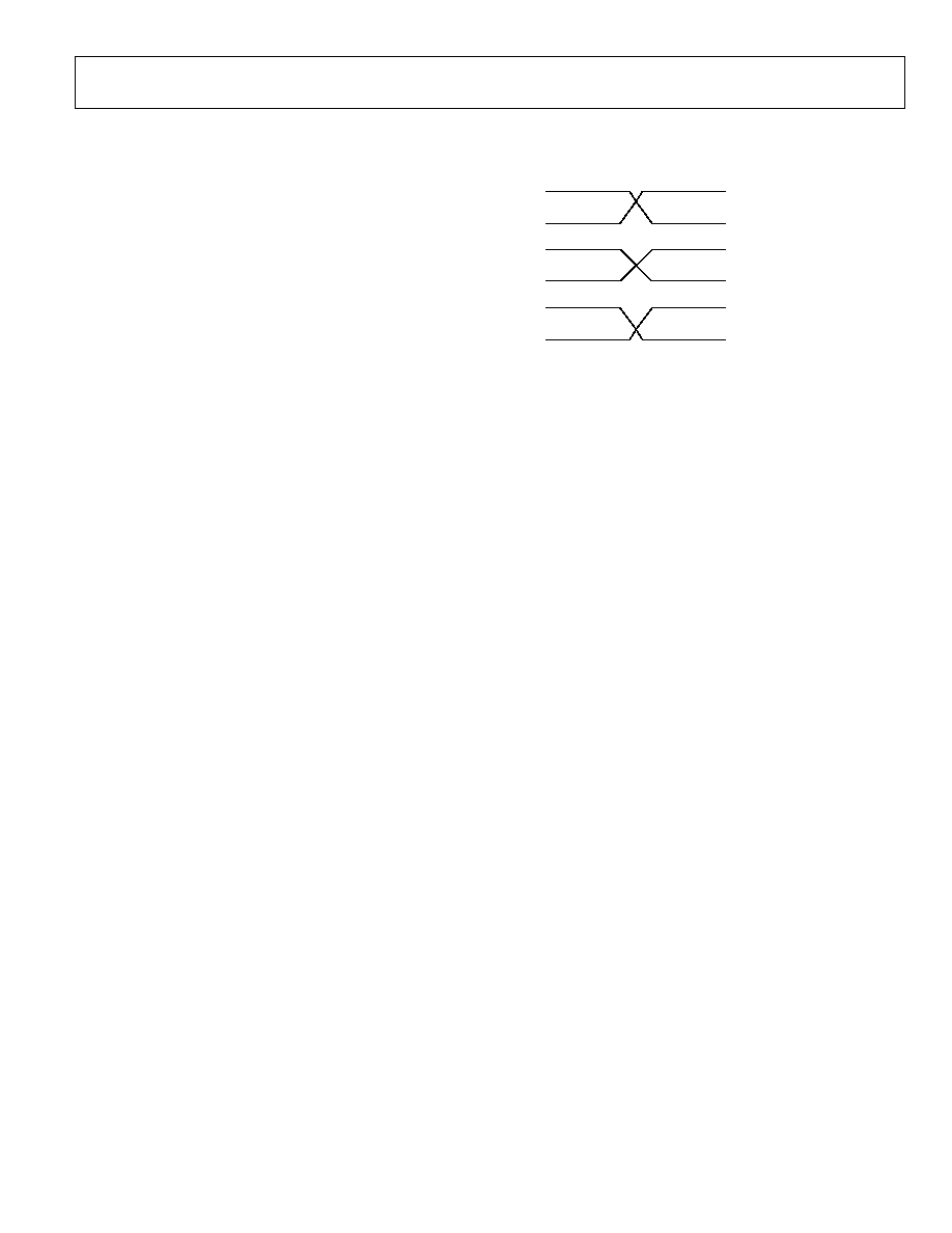
AD9734/AD9735/AD9736
Rev. 0 | Page 43 of 68
CROSS CONTROLLER REGISTERS
The AD973x differential output stage can be adjusted in order
to equalize the charge injection into the positive and negative
outputs. This adjustment can impact certain performance
characteristics, such as harmonic distortion or IMD. System
performance can be enhanced by adjusting the cross controller
as described next.
If the system is calibrated after manufacture, the cross controller
offsets may be adjusted to provide optimum performance. Start
by incrementing DNDEL<5:0> (Reg 11, Bits 5:0) while
observing HD2 (second harmonic distortion) and/or IMD to
find the desired optimum. If DNDEL does not influence the
performance, set it to 0 and increment UPDEL<5:0> (Reg 10,
Bits 5:0). Based on system characterization, it may be found that
setting one or the other of these controls to the maximum value
yields the best performance.
Figure 83 shows the effect of UPDEL and DNDEL.
04862-083
INCREMENT DNDEL TO MOVE
THE CROSSING TOWARD THE
IDEAL VALUE
IDEAL DIFFERENTIAL OUTPUT
CROSSING ALIGNMENT
INCREMENT UPDEL TO MOVE
THE CROSSING TOWARD THE
IDEAL VALUE
Figure 83. Effect of UPDEL and DNDEL
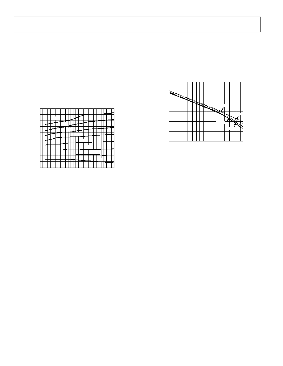
AD9734/AD9735/AD9736
Rev. 0 | Page 44 of 68
ANALOG CONTROL REGISTERS
The AD973x includes some registers for optimizing its analog
performance. These registers include temperature trim for the
band gap, noise reduction in the output current mirror, and
output current mirror headroom adjustments.
BAND GAP TEMPERATURE CHARACTERISTIC
TRIM BITS
Using TRMBG<2:0> (Reg 14, Bits 2:0) the temperature
characteristic of the internal band gap can be trimmed to
minimize the drift over temperature, as shown in Figure 84.
≠50 ≠40 ≠30 ≠20 ≠10 0 10 20 30 40 50 60 70
80 90
TEMPERATURE (
∞
C)
VREF (
V
)
1.23
1.22
1.21
1.2
1.19
1.18
04862-084
000
010
001
011
101
110
111
100
Figure 84. Band Gap Temperature Characteristic for Various TRMBG Values
The temperature changes are sensitive to process variations,
and Figure 84 may not be representative of all fabrication lots.
Optimum adjustment requires measurement of the device
operation at two temperatures and development of a trim
algorithm to program the correct TRMBG<2:0> values in
external nonvolatile memory.
MIRROR ROLL-OFF FREQUENCY CONTROL
With MSEL<1:0> (Reg 14, Bits 7:6) the user can adjust the noise
contribution of the internal current mirror to optimize the 1/f
noise. Figure 85 shows MSEL vs. the 1/f noise with 20 mA full-
scale current into a 50 resistor.
F (kHz)
NOI
SE (
I
dBm/
Hz)
≠110
≠115
≠120
≠125
≠130
≠140
≠135
1
10
100
04862-0-085
MSEL0
MSEL2
MSEL1
MSEL3
Figure 85. 1/f Noise with Respect to MSEL Bits
HEADROOM BITS
HDRM<7:0> (Reg 15, Bits 7:0) are for internal evaluation. It is
not recommended to change the default reset values.
AD9734/AD9735/AD9736
Rev. 0 | Page 45 of 68
VOLTAGE REFERENCE
The AD973x output current is set by a combination of digital
control bits and the I120 reference current, as shown in
Figure 86.
CURRENT
SCALING
FSC<9:0>
AD9736
DAC
IFULL-SCALE
10k
1nF
V
REF
I120
AVSS
I120
V
BG
1.2V
+
≠
04862-086
Figure 86. Voltage Reference Circuit
The reference current is obtained by forcing the band gap
voltage across an external 10 k resistor from I120 (Pin B14) to
ground. The 1.2 V nominal band gap voltage (V
REF
) generates a
120 µA reference current in the 10 k resistor. This current is
adjusted digitally by FSC<9:0> (Reg 02, Reg 03) to set the
output full-scale current I
FS
:
>
<
◊
+
◊
=
0
.
9
1024
192
72
FSC
R
V
I
REF
FS
The full-scale output current range is approximately 10 mA to
30 mA for register values from 0x000 to 0x3FF. The default
value of 0x200 generates 20 mA full scale. The typical range is
shown in Figure 87.
35
30
25
20
I
FS
(mA)
15
10
5
0
0
200
400
600
800
DAC GAIN CODE
1000
04862-
087
Figure 87. I
FS
vs. DAC Gain Code
Always connect a 10 k resistor from the I120 pin to ground
and use the digital controls to vary the full-scale current. The
AD973x is not a multiplying DAC. Applying an analog signal to
I120 is not supported.
VREF (Pin C14) must be bypassed to ground with a 1 nF
capacitor. The band gap voltage is present on this pin and may
be buffered for use in external circuitry. The typical output
impedance is near 5 k. If desired, an external reference may be
used to overdrive the internal reference by connecting it to the
VREF pin.
IPTAT (Pin D14) is used for factory testing. It should be left
floating.
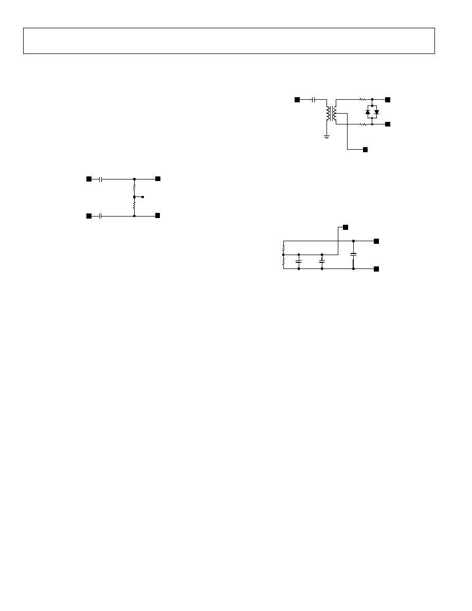
AD9734/AD9735/AD9736
Rev. 0 | Page 46 of 68
APPLICATIONS INFORMATION
DRIVING THE DACCLK INPUT
The DACCLK input requires a low jitter differential drive
signal. It is a PMOS input differential pair powered from the
1.8 V supply, so it is important to maintain the specified 400
mV input common-mode voltage. Each input pin can safely
swing from 200 mV p-p to 800 mV p-p about the 400 mV
common-mode voltage. While these input levels are not directly
LVDS compatible, DACCLK may be driven by an offset ac-
coupled LVDS signal, as shown in Figure 88.
04862-088
LVDS_P_IN
CLK+
50
50
0.1
µ
F
0.1
µ
F
LVDS_N_IN
CLK≠
V
CM
= 400mV
Figure 88. LVDS DACCLK Drive Circuit
If a clean sine clock is available, it may be transformer-coupled
to DACCLK, as shown in Figure 105. Use of a CMOS or TTL
clock may also be acceptable for lower sample rates. It can be
routed through a CMOS to LVDS translator, then ac-coupled, as
described previously. Alternatively, it may be transformer-
coupled and clamped, as shown in Figure 89.
04862-089
50
50
TTL OR CMOS
CLK INPUT
CLK+
CLK≠
V
CM
= 400mV
BAV99ZXCT
HIGH SPEED
DUAL DIODE
0.1
µ
F
Figure 89. TTL or CMOS DACCLK Drive Circuit
A simple bias network for generating V
CM
is shown in
Figure 90. It is important to use CVDD18 and CVSS for the
clock bias circuit. Any noise or other signal that is coupled onto
the clock is multiplied by the DAC digital input signal and may
degrade the DAC's performance.
04862-090
0.1
µ
F
1nF
1nF
V
CM
= 400mV
VDDC
1.8V
VSSC
1k
287
Figure 90. DACCLK V
CM
Generator Circuit
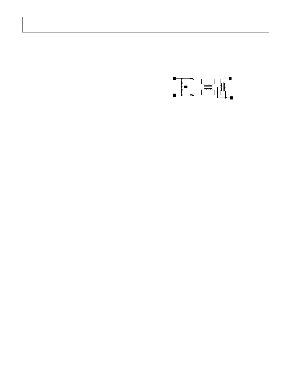
AD9734/AD9735/AD9736
Rev. 0 | Page 47 of 68
DAC OUTPUT DISTORTION SOURCES
The second harmonic is mostly due to an imbalance in the
output load. The dc transfer characteristic of the DAC is capable
of second-harmonic distortion of at least -75 dBc. Output load
imbalance or digital data noise coupling onto DACCLK causes
additional second-harmonic distortion.
The DAC architecture inherently generates third harmonics, the
levels of which depend on the output frequency and amplitude
being generated. If any output signal is rectified and coupled
back onto the DAC clock, it can generate additional third-
harmonic energy.
The distortion components should be identical in amplitude
and phase at both AD973x outputs. Even though each single-
ended output includes a large amount of second-harmonic
energy, a careful differential-to-single-ended conversion can
remove most of it. Optimum performance at high intermediate
frequency (IF) outputs is obtained with the output circuit
shown in Figure 91. This is the configuration implemented on
the evaluation board (Figure 105). The 20 series resistors
allow the DAC to drive a less reactive load, which improves
distortion. Further improvement can be made by adding the
balun T3 to help provide an equal load to both DAC outputs.
04862-091
IOUTA
IOUTB
J2, 50
OUTPUT
AVSS
R17
20
1
5
6
5
1
3
4
4
3
R19
20
T3
T1
AVSS
R8
50
R6
50
Figure 91. IF Signal Output Circuit
Because T1 has a differential input but a single-ended output,
Pin 4 of T1 has a higher capacitance to ground due to parasitics
to Pin 3. T1 Pin 6 has lower parasitic capacitance to ground
because it drives 50 at Pin 1. This presents an unbalanced
load to the DAC output, so T3 is added to improve the load
balancing. Refer to Figure 105 for the transformer part
numbers.
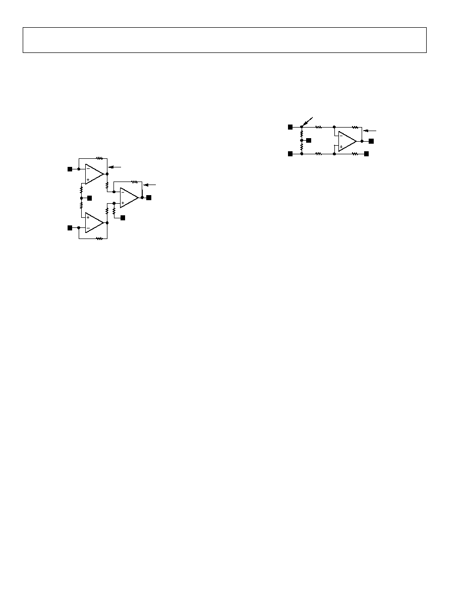
AD9734/AD9735/AD9736
Rev. 0 | Page 48 of 68
DC-COUPLED DAC OUTPUTS
In some cases, it may be desirable to dc-couple the AD973x
outputs. The best method for doing this is shown in Figure 92.
This circuit can be used with voltage or current feedback
amplifiers. Because the DAC output current is driving a virtual
ground, this circuit may offer enhanced settling times. The
settling time is limited by the op amp rather than the DAC. This
circuit is intended for use where the amplifiers can be powered
by a bipolar supply.
04862-092
IOUTA
DAC
OUTPUT
20mA
FULL SCALE
IOUTB
100
100
100
500
500
100
500
500
AVSS
AVSS
OUTPUT
2V p-p
+1V TO ≠1V
2V p-p
0V TO ≠2V
Figure 92. Op Amp I to V Conversion Output Circuit
An alternate circuit is shown in Figure 93. It suffers from dc
offset at the output unless the DAC load resistors are small,
relative to the amplifier gain and feedback resistors.
04862-093
IOUTA
OUTPUT
AVSS
IOUTB
25
25
2k
AVSS
2k
1k
1k
DAC OUTPUT
20mA
FULL SCALE
2V p-p
0V TO ≠2V
0.5V p-p
0V TO ≠0.5V
Figure 93. Differential Op Amp Output Circuit
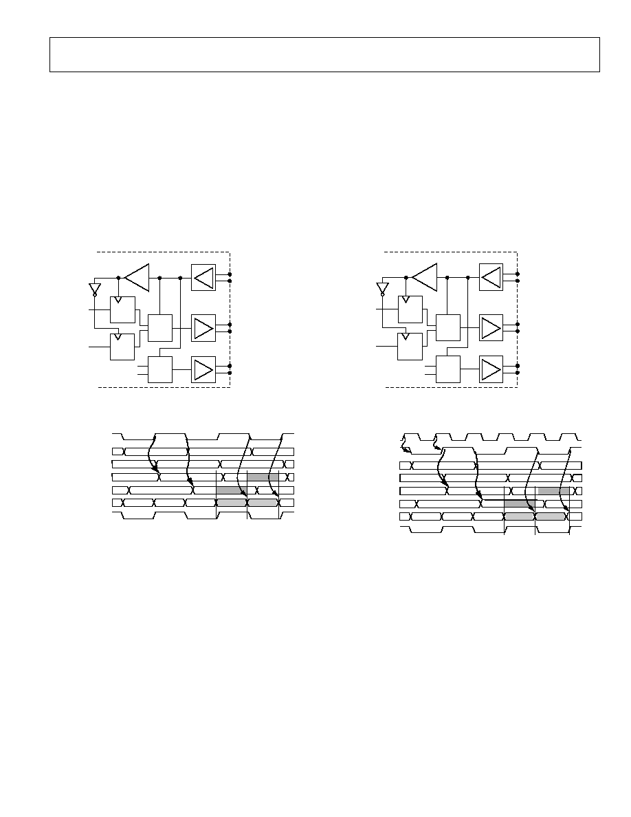
AD9734/AD9735/AD9736
Rev. 0 | Page 49 of 68
DAC DATA SOURCES
The circuit shown in Figure 94 allows optimum data alignment
when running the AD973x at full speed. This circuit can be
easily implemented in the FPGA or ASIC used to drive the
digital inputs. It is important to use the DATACLK_OUT signal
because it helps to cancel some of the timing errors. In this
configuration, DATACLK_OUT generates the DDR LVDS
DATACLK_IN to drive the AD973x. The circuit aligns the
DATACLK_IN and the digital input data (DB<13:0>) as
required by the AD973x. The LVDS controller in the AD973x
uses DATACLK_IN to generate the internal DSS to capture the
incoming data in the center of the valid data window.
04862-094
MUX
MUX
D1
DATACLK_OUT
FROM AD9736 (DDR)
DATACLK_IN
TO AD9736 (DDR)
DB(13:0) TO AD9736
DATA SOURCE
LOGIC 0
LOGIC 1
DATA2
DATA1
D2
Figure 94. Recommended FPGA/ASIC Configuration for Driving AD973x
Digital Inputs, 1◊ Mode
04862-095
DATA1
DATA2
A
C
A
C
E
B
A
B
C
D
B
D
D1
D2
DB
DATACLK_OUT+
DATACLK_IN+
Figure 95. FPGA/ASIC Timing for Driving AD973x Digital Inputs, 1◊ Mode
To operate in 2◊ mode, the circuit in Figure 94 must be
modified to include a divide-by-2 block in the path of
DATACLK_OUT. Without this additional divider, the data and
DATACLK_IN runs 2◊ too fast. DATACLK_OUT is always
DACCLK/2.
Contact FPGA vendors directly regarding the maximum output
data rates supported by their products.
04862-096
MUX
MUX
D1
DATACLK_OUT
FROM AD9736 (DDR)
DATACLK_IN
TO AD9736 (DDR)
DB(13:0) TO AD9736
DATA SOURCE
LOGIC 1
LOGIC 0
DATA2
DATA1
D2
˜
2
Figure 96. Recommended FPGA/ASIC Configuration for Driving AD973x
Digital Inputs, 2◊ Mode
04862-097
CLK_OUT+/2
DATA2
DATA1
A
C
A
C
E
B
A
B
C
D
B
D
D1
D2
DB
DATACLK_OUT+
DATACLK_IN+
Figure 97. FPGA/ASIC Timing for Driving AD973x Digital Inputs, 2◊ Mode
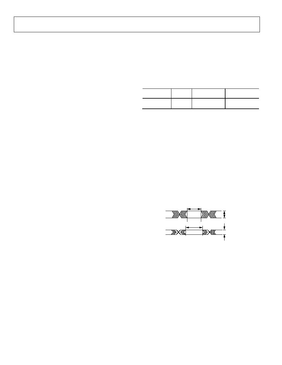
AD9734/AD9735/AD9736
Rev. 0 | Page 50 of 68
INPUT DATA TIMING
The AD973x is intended to operate with the LVDS and sync
controllers running to compensate for timing drift due to
voltage and temperature variations. In this mode, the key to
correct data capture is to present valid data for a minimum
amount of time. The AD973x minimum valid data time was
measured by increasing the input data rate to the point of
failure. The nominal supply voltages were used and the
temperature was set to the worst case of 85∞C. The input
data was verified via the BIST signature registers, because the
DAC output does not run as fast as the input data logic. The
following example explains how the minimum data valid
period is calculated for the typical performance case.
These factors must be considered in determining the minimum
valid data window at the receiver input:
∑
Data rise and fall times: 100 ps (rise + fall)
∑
Internal clock jitter: 10 ps (DATACLK_OUT +
DATACLK_IN)
∑
Bit-to-bit skew: 50 ps
∑
Bit-to-DATACLK_IN skew: 50 ps
∑
Internal data sampling signal resolution: 80 ps
For nominal silicon, the BIST typically indicates failure at
2.15 GSPS or a DACCLK period of 465 ps. The valid data
window is calculated by subtracting all the other variables
from the total data period:
Minimum Data Valid Time = DACCLK Period - Data Rise -
Data Fall - Jitter - Bit-to-Bit Skew - Bit-to-DATACLK_IN Skew
- Data Sampling Signal Resolution
For the 400 mV p-p LVDS signal case:
Minimum Data Valid = 465 ps - 100 ps - 10 ps - 50 ps - 80 ps
= 465 ps - 240 ps = 225 ps
For correct data capture, the input data must be valid for 225 ps.
Slower edges, more jitter, or more skew require an increase in
the clock period to maintain the minimum data valid period.
Table 26 shows the typical minimum data valid period (t
MDE
) for
400 mV p-p differential and 250 mV p-p differential LVDS
swings.
The ability of the AD973x to capture incoming data is
dependent on the speed of the silicon, which varies from lot to
lot. The typical (or average) silicon speed operates with data
that is valid for 225 ps at 85∞C. Statistically, the worst extreme
for slow silicon may require up to a 344 ps valid data period, as
specified in Table 2.
Table 26. Typical Minimum Data Valid Times
Differential
Input Voltage
BIST
Max f
CLK
Min Clock Period
Typ Min Data
Valid at Receiver
400 mV
2.15 GHz
465 ps
225 ps
250 mV
2.00 GHz
500 ps
260 ps
At 1.2 GHz, the typical 400 mV p-p minimum data valid period
of 225 ps leaves 608 ps for external factors. Under the same
conditions, the worst expected minimum data valid period of
344 ps leaves 489 ps for external data uncertainty.
The 100 mV LVDS V
od
threshold test is a dc test to verify that
the input logic state changes. It does not indicate the operating
speed. The receiver's ability to recover the data depends on
the input signal overdrive. With a 250 mV input, there is a
150 mV overdrive, and with a 400 mV signal, there is a 300 mV
overdrive. The relationship between overdrive level and timing
is very nonlinear. Higher levels of overdrive result in smaller
minimum valid data windows.
For typical silicon, decreasing the LVDS swing from 400 mV p-p
to 250 mV p-p requires the minimum data valid period to
increase by 15%. This is illustrated in Figure 98.
225ps
400mV
260ps
250mV
04862-098
Figure 98. Typical Minimum Valid Data Time (t
MDE
) vs. LVDS Swing
The minimum valid data window changes with temperature,
voltage, and process. The maximum value presented in the
specification table was determined from a 6 distribution in the
worst-case conditions.
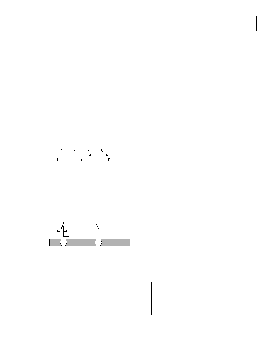
AD9734/AD9735/AD9736
Rev. 0 | Page 51 of 68
SYNCHRONIZATION TIMING
When more than one AD973x must be synchronized or when
a constant group delay must be maintained, the internal
controllers cannot be used. If the FIFO is enabled, the delay
between multiple AD973x devices is unknown. If the
DATACLK_OUT from multiple devices is used, there is an
uncertainty of two DACCLK periods because the initial phase
of DATACLK_OUT with respect to DACCLK cannot be
controlled. This means one DAC must be used to provide
DATACLK_OUT for all synchronized DACs and all timing
must be externally managed. The following timing information
allows system timing to be calculated so that multiple AD973xs
can be synchronized.
DATACLK_OUT changes relative to the rising edge of
DACCLK+ and is delayed, as shown in Figure 99. Because
DACCLK is divided by 2 to create DATACLK_OUT, the phase
of DATACLK_OUT can be 0∞ or 180∞. There is no way to
predict or control this relationship. It may be different after each
power cycle and is not affected by hardware or software resets.
t
DDCO
DACCLK
DATACLK_OUT
04862-099
Figure 99. DACCLK to DATACLK_OUT Delay
The incoming data is de-interleaved internally as shown in
Figure 76. Each edge of DATACLK_IN latches an incoming
sample in two alternating registers. The DATACLK_IN to data
setup and hold definitions are illustrated in Figure 100. All the
data inputs must be valid during the setup-and-hold period.
External skew effectively increases the setup and hold times that
the data source must meet.
04862-
100
DATACLK_IN
OR DATACLK_OUT
DATA_IN
t
DH
t
DSU
Figure 100. Standard Definitions for DATACLK_IN or DATACLK_OUT to
Data Setup and Hold, SD = 0
While correct DATA_IN vs. DATACLK_IN timing is critical,
the transition of the incoming data to the DACCLK domain is
equally critical. By referencing the incoming DATA and
DATACLK_IN timing to the DATACLK_OUT signal, some
timing uncertainty can be removed. The DATACLK_OUT
timing very closely tracks the timing of the DACCLK-
controlled registers. Any variation in the path delay affects both
paths in almost the same way. If DATACLK_OUT is not used,
the full DACCLK to DATACLK_OUT path variation reduces
the external timing margin. Figure 101 shows a simplified view
of the internal clocking scheme with the relevant delay paths.
The internal architecture is interleaved such that each phase has
twice as long to make the transition across the clock domains.
This results in an extremely narrow window where the
incoming data must be held stable.
Table 27 shows the timing parameters for Figure 99 and
Figure 100. These parameters were measured for a sample of
five devices from five silicon lots. Worst-case fast and slow skew
lots were included in addition to the nominal (or average) lot.
The typical -40∞C to typical +85∞C spread illustrates the
variability with temperature for a single lot. Adding in lot-to-lot
variation with the fast and slow lots indicates the worst-case
spread in timing.
The timing varies such that all of the parameters move in the
same direction. For example, if the DATACLK_IN to data setup
time is fast, the hold time is similarly fast. The DACCLK to
DATACLK_OUT delay and the DATACLK_OUT to data setup
and hold is also at the fast end of the range.
Note that the polarities of setup-and-hold values in Table 27
conform to the standard convention of setup time occurring
prior to the latching edge and hold time occurring after the
latching edge, as shown in Figure 100.
Table 27. AD973x Clock and Data Timing Parameters
Symbol and Definition
Fast -40∞C
Typ -40∞C
All +25∞C
Typ +85∞C
Slow +85∞C
Unit
t
DDCO
- DACCLK to DATACLK_OUT Delay
1650
1800
1890
2050
2350
ps
t
DCISU
- DATACLK_IN to DATA Setup
-100
-120
-150
-170
-220
ps
t
DCIH
- DATACLK_IN to DATA Hold
210
220
240
280
360
ps
t
DISU
- DATACLK_OUT to DATA Setup
1310
1440
1611
1710
1970
ps
t
DIH
- DATACLK_OUT to DATA Hold
-1250
-1360
-1548
-1640
-1890
ps
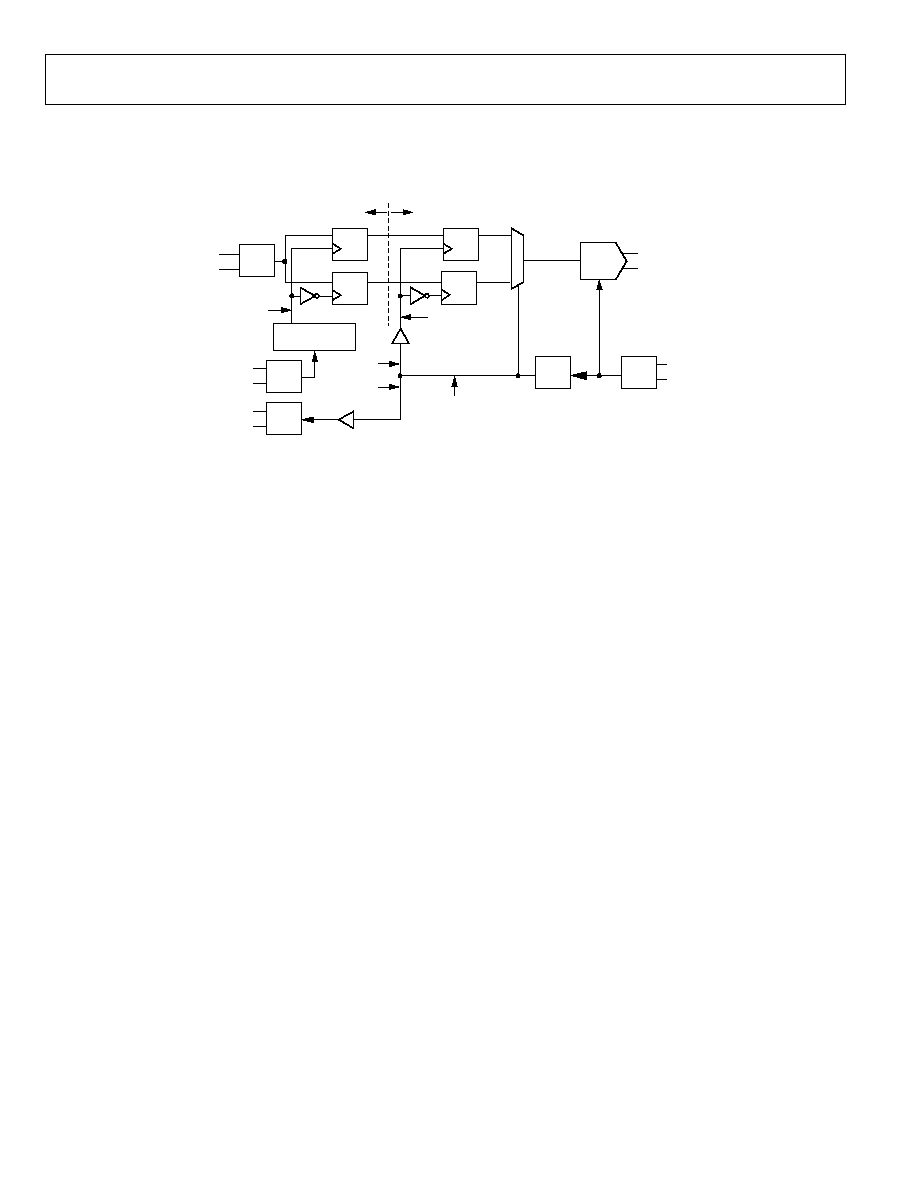
AD9734/AD9735/AD9736
Rev. 0 | Page 52 of 68
POWER SUPPLY SEQUENCING
The 1.8 V supplies should be enabled simultaneously with or prior to the 3.3 V supplies. Do not enable the 3.3 V supplies when the
1.8 V supplies are off.
04862-101
LVDS
RX
DATACLK_IN
DATACLK_IN DOMAIN
DACCLK DOMAIN
DB<13:0>
PATH A
PATH B
DATACLK_OUT
D1A
DAC_DATA
DAC_OUTPUT
D1
D2
D2A
SD<3:0>
SAMPLE DELAY
DACCLK
FF
FF
˜
2
CLK
RX
FF
FF
SD<3:0>
SAMPLE DELAY
DATA SAMPLING
SIGNAL
DAC SAMPLING
SIGNAL
COMMON SYSTEM CLOCK
DELAYS THROUGH PATH A AND B WILL TRACK,
THUS REDUCING TIMING UNCERTAINTY IN THE SYSTEM
LVDS
RX
LVDS
TX
DAC
CORE
Figure 101. Simplified Internal Clock Routing
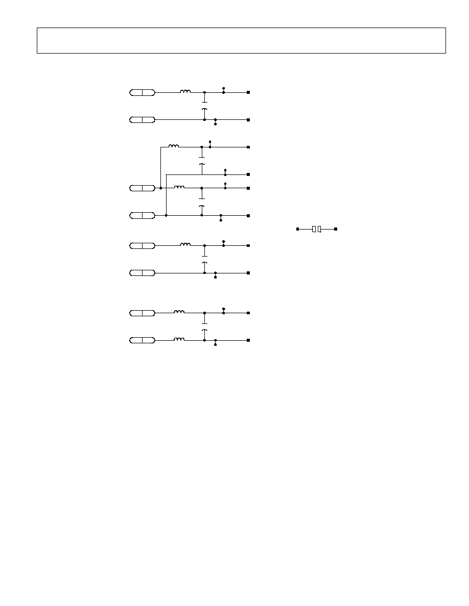
AD9734/AD9735/AD9736
Rev. 0 | Page 53 of 68
AD973
X
EVALUATION BOARD SCHEMATICS
L1, L3, L4, L5, L6, AND L7
FERRITE BEAD CORE:
PANASONIC EXC≠CL3225U1
DIGIKEY PN: P9811CT≠ND
DVSS
TP5
BLK
33DIG
VSS
TB1
1
TB1
2
L6
FERRITE
TP4
RED
DVDD33
LC1210
C14
10
µ
F
6.3V
ACASE
+
AVSS
TP3
BLK
33ANA
AVSS
TB2
1
TB2
2
L1
FERRITE
TP1
RED
VDDA33
LC1210
C1
10
µ
F
6.3V
ACASE
+
AVSS
TP11
BLK
18ANA
AVSS
TB2
3
TB2
4
L3
FERRITE
TP9
RED
VDDC
LC1210
C10
10
µ
F
6.3V
L4
FERRITE
LC1210
ACASE
+
DVSS
TP13
BLK
TP6
RED
TP14
BLK
VDD18A
VDD18B
DVSS
TP7
RED
C22
10
µ
F
6.3V
L7
FERRITE
LC1210
L5
FERRITE
LC1210
18DIG
TB1
3
VSS
TB1
4
ACASE
+
C18
10
µ
F
6.3V
ACASE
+
POWER INPUT FILTERS
AVSS
VSS
UNDER DUT
JP1
04862≠102
Figure 102. Power Supply Inputs for AD973x Evaluation Board, Rev. F
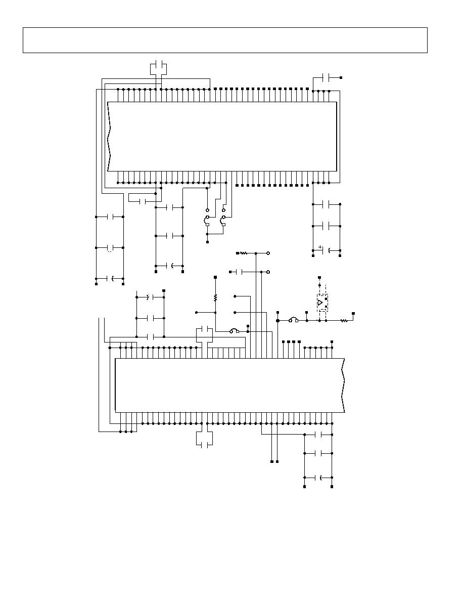
AD9734/AD9735/AD9736
Rev. 0 | Page 54 of 68
IN1
IN2
IN3 IN4
IP1
A8
B8
C8
D8
A9
C4
1N
F
0
.1
µ
F
4.7
µ
F
C1
9
4.7
µ
F
6.3V
VSSA
VD
D
18B
VSS
C2
3
4.7
µ
F
6.3V
C2
4
0.1
µ
F
C2
5
1nF
H1
V
DD1
V
DD2
V
DD3
V
DD5
V
DD4
V
DD6
V
DD7
V
DD8
VSS1
VSS2
VSS3
VSS4
VSS5
VSS6
VSS7
VSS8
VSS9
VSS10
VSS21
NCK1
VSS22
V
DD1
6
V
DD1
5
V
DD1
4
V
DD1
2
V
DD1
3
V
DD1
1
V
DD1
0
V
DD9
VSS20
VSS19
VSS18
VSS17
VSS16
VSS15
VSS14
VSS13
VSS12
V
S
S
1
1
LVD
S
13N
LVD
S
13P
LVD
S
12N
LVD
S
12P
LVD
S
11N
LVD
S
11P
LVD
S
10N
LVD
S
10P
LVDS9N
LVDS9P
LVDS8N
LVDS8P
LVDS7N
LVDS7P
LVDS6N
LVDS6P
LVD
S
13N
LVD
S
13N
LVD
S
13N
LVD
S
13N
SPI_M
OD
E
LVDS0N
LVDS0P
LVDS1N
LVDS1P
LVDS2N
LVDS2P
LVDS3N
LVDS3P
LVDS4N
LVDS4P
LVDS5N
LVDS5P
LV
DCLKOUTN_
V
D
S
C
LKINN
LV
DCLKOUTN_
V
D
S
C
LKINP
VD
D
331
VD
D
332
VD
D
333
VD
D
334
BOTTOM
H2
H3
H4
J1
J2
J3
J4
K3
K4
L3
L4
L5
L6
M3
M4
M5
M6
K2
K1
L2
L1 M2
M1
N1
P1
N2
N3
P2
P3
N4
P4
N5
P5
N6
P
6
L7
M7
N7
P7
H1
4
H1
3
H1
2
H1
1
J14
J13
J12
J11
K1
1
K1
2
L9
L10
L11
L12
M9
M1
0
M1
1
M1
2
K2
K1
L2
L1 M2
M1
N1
P1
N2
N3
P2
P3
N4
P4
N5
P5
N6
P
6
L7
M7
N7
P7
VSS
C3
4
C2
0
0.1
µ
F
C2
1
1nF
C3
6.3V
VD
D
18A
C7
DNP
VSS
V
DD3
3
A 2
3
B
C2
C6
IRQ
IPTAT
INF
S
P
ARE
C9
R1
6
10k
TP2 WHT
TP12 WHT
WHT TP8
WHT TP10
TP16 WHT
JP4
IRQ
R
ESET_A
R
ESET
SPC
SB
SPSD
I
JP3
4
3
SW
1
V
DD3
VSS;
5
VSS
SPC
LK
SPSD
O
VR
EF
I120
V
DD3
3
CC060
A1
0
A1
1
B9
B1
0
B1
1
C9
C1
0
C1
1
D9
D1
0
D1
1
A1
2
A1
3
B1
2
B1
3
C1
2
C1
3
D1
2
D1
3
A1
4
IP2
IP3 IP4
TOP
3
3
A
D
D
V
3
3
D
D
V
A5
A4
VSSA
331
VSSA
332
VSSA
333
VSSA
334
VSSA
335
VSSA
336
VSSA
337
VSSA
338
VSSA
339
VSSA
3310
VSSA
3311
VSSA
3312
V
DDC1
V
DDC2
V
DDC3
V
DDC4
V
DDC5
V
DDC6
V
DDC7
V
DDC8
V
DDC9
V
D
D
C
1
0
V
DDC1
1
VSSC
1
CLKN
CLKP
VSSC
2
VSSC
3
VSSC
4
VSSC
5
VSSC
6
VSSC
7
VSSC
8
VSSC
11
V
DDA3
3
1
V
DDA3
3
2
V
DDA3
3
3
V
DDA3
3
4
V
DDA3
3
5
V
DDA3
3
6
V
DDA3
3
7
V
DDA3
3
8
S
P
ARE
I
1
2
0
VR
EF
SIGNED_IRQ
PD
_R
ESET
2X_C
SB
FIFO_DSIO
FS
CO_
S
CLK
FSC
1_SD
O
SH
IELD
1
SH
IELD
2
SH
IELD
3
SH
IELD
4
SH
IELD
5
SH
IELD
6
HY
DROGE
N
U1
U1
HY
DROGE
N
VSSA
R5
10k
R
C
1206
VSSA
3314
VSSA
3313
VSSA
3315
VSSA
3316
VSSA
3317
VSSA
3318
VSSA
3319
VSSA
3320
VSSA
3321
VSSA
3322
VSSA
3333
VSSA
3324
B4
D6
D5
D4
C6
C5
C4
D1
E1
F1
E2
E3
E4
F2
F3
F4
G1
G2
G3
G4
D3
C2
C1
B2
B1
A3
A2
D2
D1
4
E13
E14
F13
F14
G13
G14
E11
E12 F11
F12
G11
G12
C1
4
B1
4
A6
B5
A1
C5
CC063
DNP
C3
B6
B3
S
S
V
1
2
DB0
N
DB0
P
DB1
N
DB1
P
DB2
N
DB2
P
DB3
N
DB3
P
DB4
N
DB4
P
DB5
N
DB5
P
DB6
N
DB6
P
DB7
N
DB7
P
DCS
KNIN
DCLKP
IN
N
I
P
I
AD9736
AD9736
A7
B7
C7
D7
CLKN
CLKP
V
DDC
C1
1
VSS
4.7
µ
F
C1
2
0.1
µ
F
C1
3
1nF
A
C
A
S
E
CC0603
CC0603
CC0603
CC0603
CC0603
CC0603
CC0603
CC0603
CC0603
VSSA
VSSA
D
B
13N
D
B
13P
D
B
12N
D
B
12P
D
B
11N
D
B
11P
D
B
10N
D
B
10P
DB9
N
DB9
P
DB8
N
DB8
P
DCLKNOUT
DCLKP
OUT
R1 0.1% 10k
CC0603
R
C
0603
CC0603
CC0603
CC0603
CC0603
A 2
3
B
ACASE
ACASE
ACASE
ACASE
N
O
TE:
A
D
9736 M
S
B
≠
LSB
B
I
T OR
D
E
R
IS R
EVER
SED
FROM THE
CONNE
CTOR BIT ORDE
R.
04862-103
Figure 103. Circuitry Local to AD973x, Evaluation Board, Rev. F
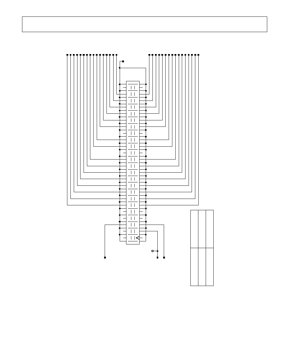
AD9734/AD9735/AD9736
Rev. 0 | Page 55 of 68
D
B
13N
D
B
12N
D
B
13P
D
B
12P
VSS
D
B
11P
D
B
10P
DB8
P
DB7
P
DB7
N
DB6
N
DB0
N
DB1
N
DB2
N
DB3
N
DB4
N
DB5
N
DB0
P
DB1
P
DB2
P
DB3
P
DB4
P
DB5
P
G2
S2
G3
G4
S3
S4
G5
G6
S5
S6
G7
G8
S7
S8
G9
G10
S9
S10
G11
G1
2
S11
S12
G13
G1
4
S13
S14
G15
G1
6
S15
S16
G17
G1
8
S17
S18
G19
G2
0
S19
S20
G21
G2
2
S21
S22
G23
G2
4
S23
S24
G25
G2
6
S25
S26
G27
G2
8
S27
S28
G29
G3
0
S29
S30
G31
G3
2
S31
S32
G33
G3
4
S33
S34
G35
G3
6
S35
S36
G37
G3
8
S37
S38
G39
G4
0
S39
S40
G41
G4
2
S41
S42
G43
G4
4
S43
S44
G45
G4
6
S45
S46
G47
G4
8
S47
S48
G49
G5
0
G1
S1
J3
DCLKNIN
DCLKNOUT
DB8
N
DB9
N
D
B
10N
D
B
11N
DB6
P
DCLKP
IN
DCLKP
OUT
DB9
P
TESTOU
TN
EXTC
L
K
TESTOU
TP
N
O
TE:
A
D
9736 M
S
B
-
LSB
B
I
T OR
D
E
R
IS R
EVER
SED
FROM THE
CONNE
CTOR BIT ORDE
R.
CONNE
CTOR
DB1
3
DB0
A
D
9736
DB0
DB1
3
TP15 WHT
JACK
JACK
FC
N≠268 F
024≠G
/0 D
04862
≠104
Figure 104. High Speed Digital I/O Connector, AD973x Evaluation Board, Rev. F
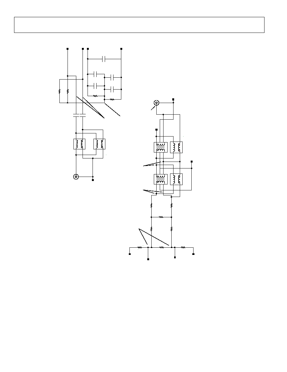
AD9734/AD9735/AD9736
Rev. 0 | Page 56 of 68
S
P
SP
VSSA
6
5
3
4
2
1
1
4
3
6
J2
R4
300
3
1
5
4
750mV p-
p
550mV p-
p
550mV p-
p
580mV p-
p
415mV C
O
M
M
O
N
MODE VOLTAGE
400mV p
≠
p
NOTE
:
T1
, T3
, AND T3
B ARE
INS
T
ALLE
D,
R6
AND R8
= 5
0
,
R7
= DNP
R1
7
AND R1
9
= 2
0
,
R161 AND R162 = 0
,
J
U
MP
E
R
ADDE
D FROM T1
P
I
N 3
TO
T1
P
I
N 2
ON THE
RE
V
C E
V
A
L BOARD.
J1 VSSA
;
3
,4,5
SM
A
200U
P
VSSA
T3A
T3B
T3
ADT
L
1
≠12X
X
ET
C
1
≠1
≠1
3
S
P
NC=2
E
T
C1≠1
≠13
E
T
C1≠
1≠13
T2
ADT
2
≠1T
≠1P
5
4
1
3
P
S
NC=2
C3
5
C3
6
0.1
µ
F
0.1
µ
F
CC0603
CC0603
CC0603
CC0603
CC0603
CC0603
CC0603
R2
0
R2
1
R3
1k
R6
50
C2
6
DNP
C2
7
DNP
C3
8
1
µ
F
C2
9
1
µ
F
C2
8
0.1
µ
F
CLKP
CLKN
V
DDC
VSSA
25
25
RC0603
RC0603
RC0603
RC0603
RC0603
RC0603
RC0603
RC0603
RC0603
R7
DNP
R1
7
20
R
161
0
R
162
0
R1
8
DNP
R1
9
20
RC0603
R8
50
RC0603
RC0603
AN LV
DS
S
I
GNAL MAY
BE
US
E
D
TO DRIV
E
C3
5
AND C3
6
IF R2
0
AND R2
1
ARE
INCRE
AS
E
D
TO 5
0
E
ACH.
R1
7
AND R1
9
CAN BE
RE
MOV
E
D
AND T1
RE
P
L
ACE
D WITH A 1
:
1
TRANS
FORME
R
FOR
HIGHE
R
OUTP
UT AMP
L
ITUDE
IF MORE
H2
IS
ACCE
P
T
ABLE
(TY
P
I
CALLY
AT LOWE
R F
OUT
).
R17 AND R19 PRESENT A
MORE 'REAL' LOAD TO THE
DAC WHICH IMP
R
OV
E
S
H2
P
E
R
FORMANCE
.
T2
AND T4
B ARE
NOT P
O
P
U
LATE
D
T1
:MINI-CIRCUITS
≠3dB
:
8-
600M
H
z
≠1dB
:
13-
300M
H
z
THIS
CONFIGURATION P
R
OV
IDE
S
OP
TIMUM AC
P
E
R
FORMANCE
FOR IF S
I
GNAL GE
NE
RATION.
TYPIC
A
L
SIGN
A
L
LEVELS SH
OW
N
FOR
50
LOAD.
VSSA
VSSA
VSSA
VSSA
IN
IP
T3
:M/
A
-COM
≠1dB
:
4.5-
1000M
H
z
SP
6
5
3
4
2
1
T4B
T1
ADT
2
≠1T
≠1P
5
4
P
S
NC=2
VSSA
;
3
,4,5
SM
A
200U
P
04862
≠105
T3A IS NOT POPULATED
Figure 105. Clock Input and Analog Output, AD973x Evaluation Board, Rev. F
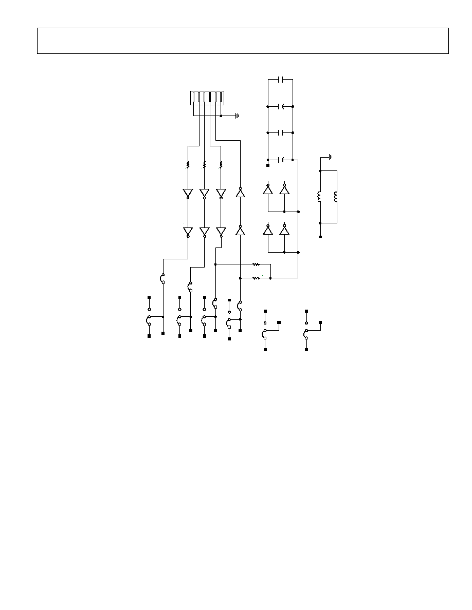
AD9734/AD9735/AD9736
Rev. 0 | Page 57 of 68
VSS
R
ESET_A
2
RC060
3
RC060
3
2
B
3
1
2
L9
6
1
2
4
5
3
P1
VSS
L8
RC0805
9k
R1
1
RC0805
9k
R1
0
RC0805
9k
R1
2
3
3
D
D
V
VSS
VSS
VSS
VSS
VSS
VSS
U
SE TH
ESE JU
M
PER
S TO SET PIN
_
M
O
D
E
CONTROL S
I
GNALS
OR CONNE
CT S
P
I
P
O
RT
SIGN
A
L
S IN
SPI_M
OD
E.
V
DD3
3
V
DD3
3
V
DD3
3
V
DD3
3
V
DD3
3
V
DD3
3
SPC
SB
SPC
LK
SPSD
I
SPSD
O
JP13
JP6
JP7
JP2
JP5
JP14
JP9
JP10
JP12
A
B
3
1
2
A
B
3
1
2
A
B
3
1
2
A
B
3
1
2
A
B
3
1
2
A
R13 10k
R14 10k
L
C
1210
L
C
1210
FERRITE
FERRITE
FE
RRITE
BE
AD CORE
:
PANASONIC EXC-CL3225U1
D
I
GIK
EY PN
:
P9811C
T-
N
D
74AC14
1
2
U5
VSS;7
V
DD33;14
74AC14
3
4
U5
VSS;7
V
DD33;14
74AC14
5
6
U5
VSS;7
V
DD33;14
74AC14
4
3
U6
VSS;7
V
DD33;14
74AC14
6
5
U6
VSS;7
V
DD33;14
74AC14
12
13
U6
VSS;7
V
DD33;14
74AC14
2
1
U6
VSS;7
V
DD33;14
74AC14
13
12
U5
VSS;7
V
DD33;14
74AC14
11
10
U5
VSS;7
V
DD33;14
74AC14
9
8
U5
VSS;7
V
DD33;14
VSS
74AC14
10
11
U6
VSS;7
V
DD33;14
74AC14
8
9
U6
VSS;7
V
DD33;14
ACASE
CC0805
+
C3
0
4.7
µ
F
6.3V
C3
1
0.1
µ
F
ACASE
CC0805
+
C3
2
4.7
µ
F
6.3V
C3
3
0.1
µ
F
SPI POR
T
04862≠
106
Figure 106. SPI Port Interface, AD973x Evaluation Board, Rev. F

AD9734/AD9735/AD9736
Rev. 0 | Page 58 of 68
AD973
X
EVALUATION BOARD PCB LAYOUT
S
ilks
c
r
e
e
n
E
r
r
o
r
:
S
P
I
&
P
I
N
a
re
r
e
ve
rse
d
.
Not
e
:
Th
e
A
D
9
7
3
6
i
s
s
o
ld
er
ed
d
i
r
e
c
t
ly
to
t
h
e
P
C
B
.
T
he
so
cke
t
i
s
n
o
t
ins
t
alle
d.
04862-107
Figure 107. CB Layout Top Placement, AD973x Evaluation Board, Rev. F
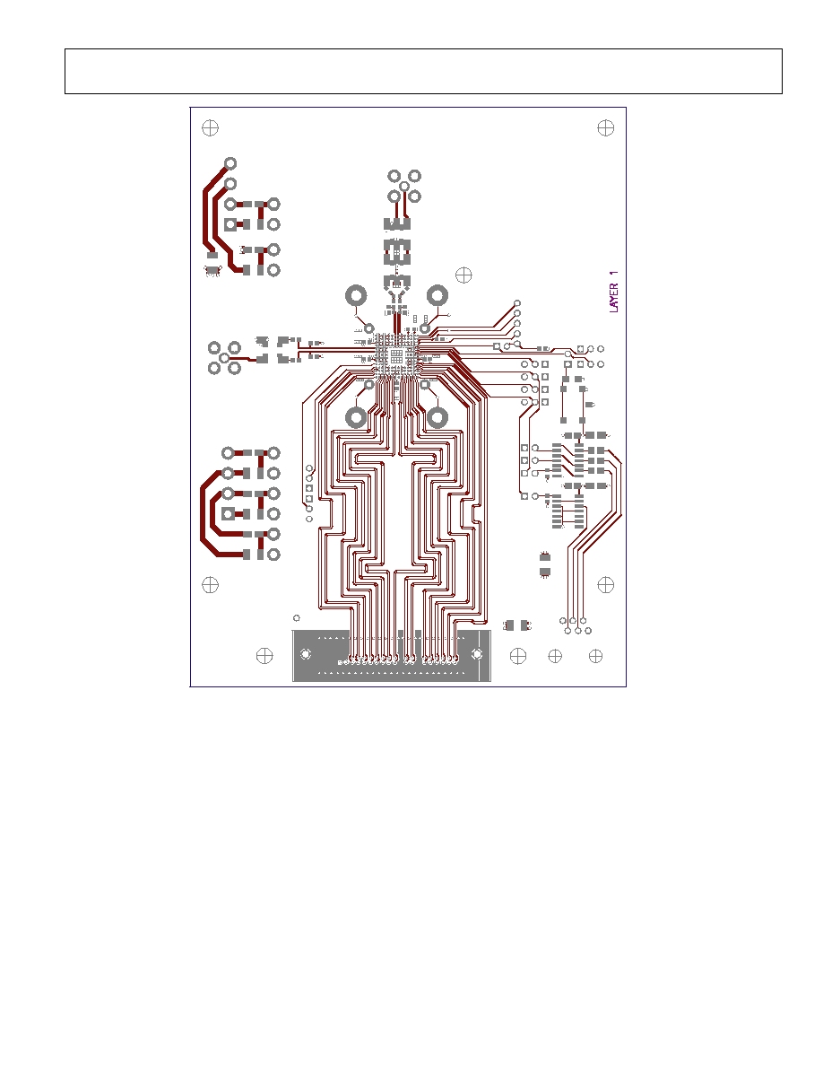
AD9734/AD9735/AD9736
Rev. 0 | Page 59 of 68
04860-108
Figure 108. PCB Layout Layer 1, AD973x Evaluation Board, Rev. F
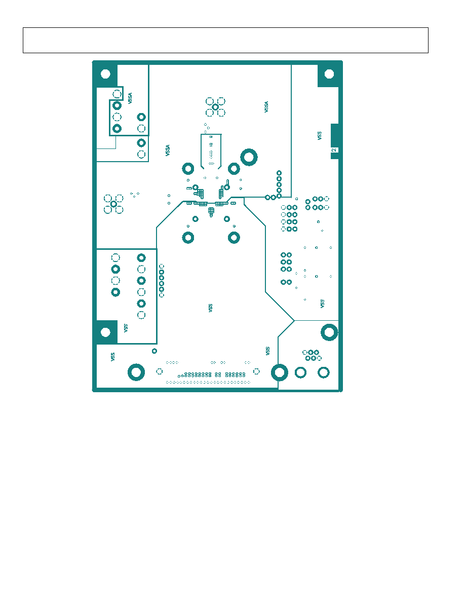
AD9734/AD9735/AD9736
Rev. 0 | Page 60 of 68
04861-109
Figure 109. PCB Layout Layer 2, AD973x Evaluation Board, Rev. F
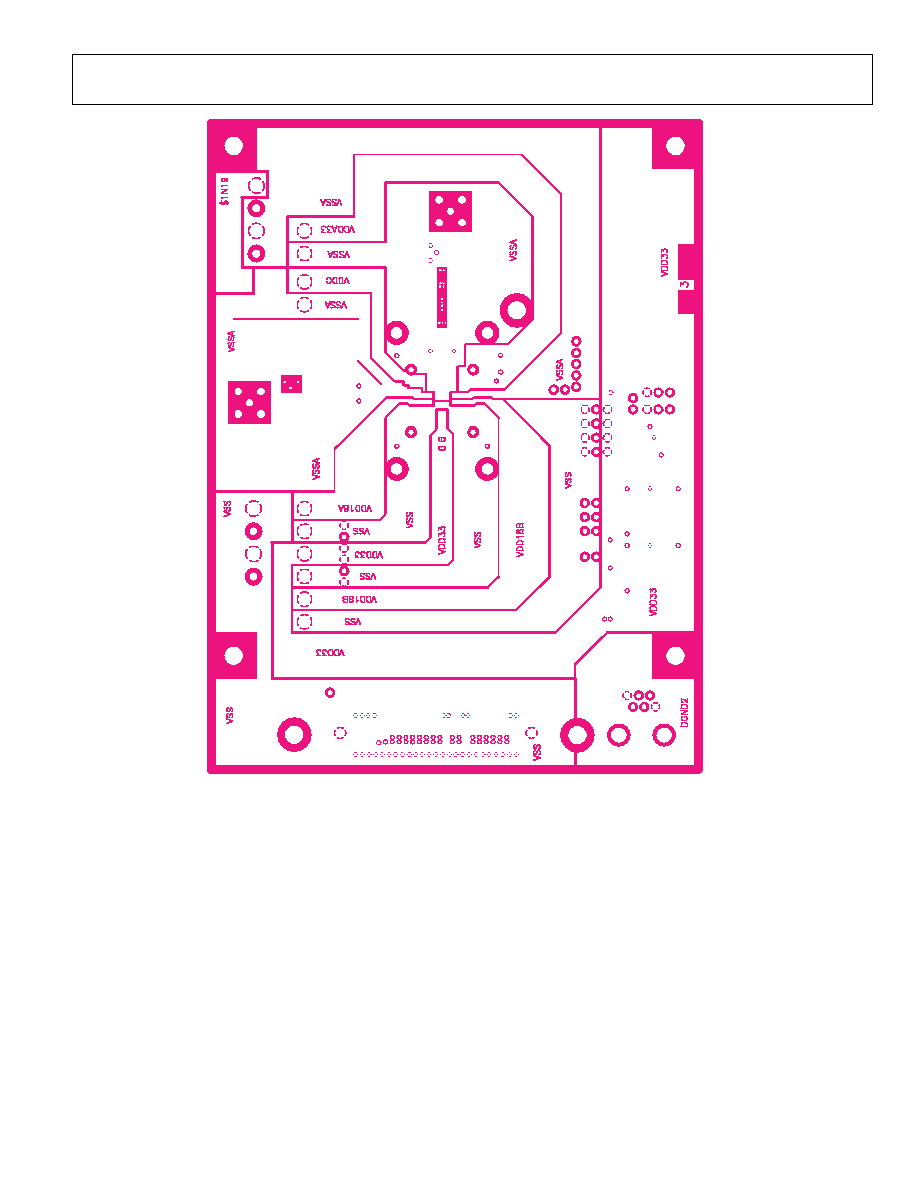
AD9734/AD9735/AD9736
Rev. 0 | Page 61 of 68
04862-110
Figure 110. PCB Layout Layer 3, AD973x Evaluation Board, Rev. F

AD9734/AD9735/AD9736
Rev. 0 | Page 62 of 68
014862-111
Figure 111. PCB Layout Layer 4, AD973x Evaluation Board, Rev. F
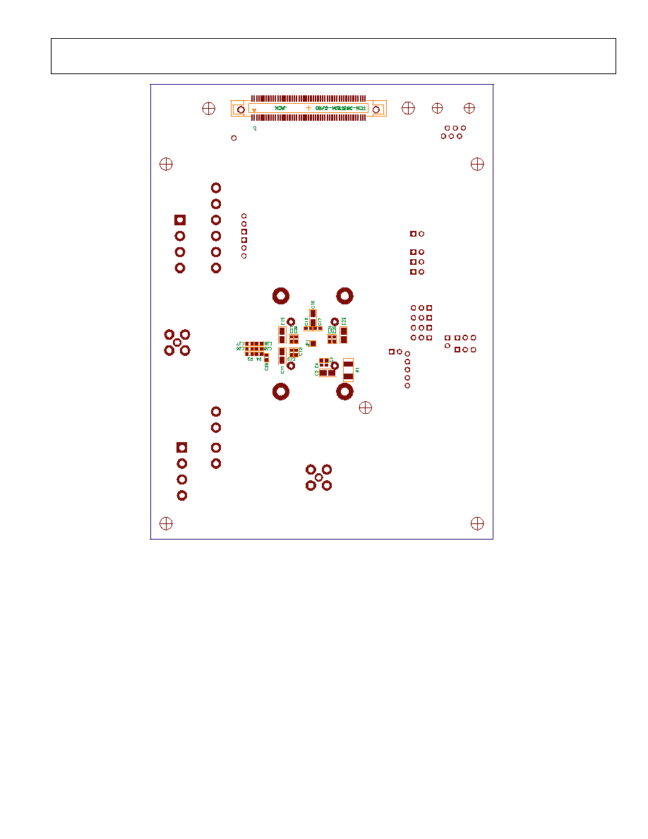
AD9734/AD9735/AD9736
Rev. 0 | Page 63 of 68
04862-112
Figure 112. PCB Layout Bottom Placement, AD973x Evaluation Board, Rev. F
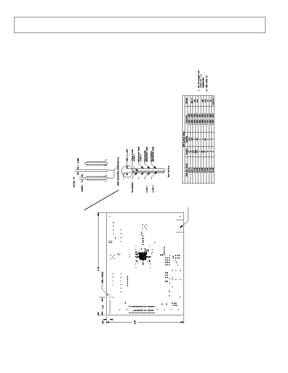
AD9734/AD9735/AD9736
Rev. 0 | Page 64 of 68
NO
T
E
:
Sp
e
c
i
a
l
l
a
y
e
r
s
t
a
c
k
t
o
s
e
t
L
V
D
S
t
ra
c
e
i
m
p
e
d
anc
e
.
04862-113
NOTE
S
1
.
MATE
RIAL: FOUR LAY
E
R
, FR4
GLAS
S
≠
E
P
O
X
Y
LAMINATE
.062 +
/
-
.007 TH
IC
K
1/4 OZ. COPPER CLAD
≠
EXTERNAL LAYERS P
L
ATE
D
TO 1
OUNCE
2 OZ. COPPER CLAD
≠ INTERNAL LAYERS
2
.
P
L
ATE
D
THRU HOLE
S
AND THE
CONDUCTIV
E
P
A
TTE
RN
ELECTROPLATED WITH .001 INCH MIN. THICK COPPER. TERMINAL AREAS AND EXPOSED PLATED THRU HOLES TO B
E
COATED WITH SOLDER AND HOT AIR LEVELED.
4. PROCESSING TOLERANCES:
A. CONDUCTIV
E
P
A
TTE
RN FRON TO BACK RE
GIS
TRATION
+/≠ .002 INCH TOTAL
B. MINIMUM ANNULAR RING S
URROUNDING HOLES .002 INCH.
C. FINISHED CONDUCTIVE PATTERN +/
≠ .0005 INCH
OF A
PER
TU
R
E
SIZE.
5. WARP AND TWIST +/
≠ .005 INCH PER INCH.
6
.
DIME
NTIONS
:
ARE
FOR THE
FINIS
H
E
D
P
ART
7. SOLD
ER
M
A
SK
:
LIQU
ID
PH
OTO IM
A
G
A
B
L
E SOLD
ER
M
A
SK
COLOR GREEN, BOTH SID
ES U
S
IN
G TH
E PA
TTER
N
(
S)
PR
OVID
ED
. N
O
M
A
SK
IS PER
M
I
TTED
ON
TH
E EXPOSED
A
R
E
A
S
. SOLD
ER
MASK TO ETCH REGISTRATION +/
≠ .002 INCH TOTAL
8. SC
R
EEN
IN
G:
SC
R
EEN
C
O
M
P
ON
EN
T OU
TLIN
ES A
N
D
NOME
NCLATURE
US
ING OP
AQUE
WHITE
INK ON THE
P
R
IMARY
AND S
E
C
ONDARY
S
I
DE
S
(AS
RE
QUIRE
D
).
NOME
NCLATURE
S
HALL BE
LE
GIBLE
. S
CRE
E
N
TO E
T
CH
REGISTRATION +/
≠ .005 INCH TOTAL.
9. SURFACES: PUNCHED OR
MACHINED SURFACES 125 MICRO
IN
C
H
ES R
M
S M
A
X.
10. BREAK ALL SHARP EDGES .015 R MAX. 1
1
.
FABRICATION V
E
NDOR TO ADD UL V
E
NDOR ID NUMBE
R
IN THIS
ARE
A ON THE
S
E
C
ONDARY
S
I
DE
1
2
.
DO NOT DRILL. FOR GOLD P
L
ATE
D
S
O
CKE
TE
D V
E
R
S
ION ONLY
.
Figure 113. PCB Fabrication Detail, AD973x Evaluation Board, Rev. F
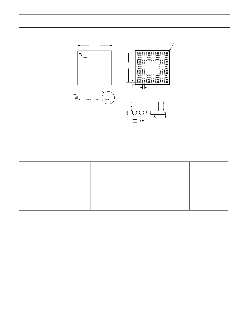
AD9734/AD9735/AD9736
Rev. 0 | Page 65 of 68
OUTLINE DIMENSIONS
12.10
12.00 SQ
11.90
SEATING
PLANE
0.43 MAX
0.25 MIN
DETAIL A
0.55
0.50
0.45
0.12 MAX
COPLANARITY
1.00 MAX
0.85 MIN
BALL DIAMETER
0.80 BSC
0.80
REF
10.40
BSC SQ
A
B
C
D
E
F
G
H
J
K
L
M
N
P
14
13
12
11
10
8
7
6
3
2
1
9
5
4
A1 CORNER
INDEX AREA
TOP VIEW
BALL A1
INDICATOR
DETAIL A
BOTTOM
VIEW
1.40 MAX
COMPLIANT TO JEDEC STANDARDS MO-205-AE.
Figure 114. 160-Lead Chip Scale Package Ball Grid Array [CSP_BGA]
(BC-160-1)
Dimensions shown in millimeters
ORDERING GUIDE
Model
Temperature Range
Description
Package Option
AD9734BBC
-40∞C to +85∞C
160-Lead Chip Scale Package Ball Grid Array (CSP_BGA)
BC-160-1
AD9734BBCRL
-40∞C to +85∞C
160-Lead Chip Scale Package Ball Grid Array (CSP_BGA)
BC-160-1
AD9734-EB
Evaluation
Board
AD9735BBC
-40∞C to +85∞C
160-Lead Chip Scale Package Ball Grid Array (CSP_BGA)
BC-160-1
AD9735BBCRL
-40∞C to +85∞C
160-Lead Chip Scale Package Ball Grid Array (CSP_BGA)
BC-160-1
AD9735-EB
Evaluation
Board
AD9736BBC
-40∞C to +85∞C
160-Lead Chip Scale Package Ball Grid Array (CSP_BGA)
BC-160-1
AD9736BBCRL
-40∞C to +85∞C
160-Lead Chip Scale Package Ball Grid Array (CSP_BGA)
BC-160-1
AD9736-EB
Evaluation Board

AD9734/AD9735/AD9736
Rev. 0 | Page 66 of 68
NOTES

AD9734/AD9735/AD9736
Rev. 0 | Page 67 of 68
NOTES

AD9734/AD9735/AD9736
Rev. 0 | Page 68 of 68
NOTES
© 2005 Analog Devices, Inc. All rights reserved. Trademarks and
registered trademarks are the property of their respective owners.
D04862≠0≠4/05(0)