 | –≠–ª–µ–∫—Ç—Ä–æ–Ω–Ω—ã–π –∫–æ–º–ø–æ–Ω–µ–Ω—Ç: AD973x | –°–∫–∞—á–∞—Ç—å:  PDF PDF  ZIP ZIP |
14/12/10-Bit, 1200 MSPS
D/A Converters
Preliminary Technical Data
AD9736/AD9735/AD9734
FEATURES
∑
1.8/3.3 V Dual Supply Operation
∑
AD9736 SFDR > 53 dBc to f
OUT
= 600 MHz
∑
AD9736 IMD > 65 dBc to f
OUT
= 600 MHz
∑
AD9736 DNL = ± 1.0 LSB
∑
AD9736 INL = ± 2.0 LSB
∑
Low power: 380 mW (I
OUTFS
= 20 mA; f
OUT
= 330 MHz)
∑
LVDS data interface with on-chip 100
terminations
∑
Analog Output: Adjustable 10-30mA (RL=25
to 50 )
∑
On-Chip 1.2 V Reference
∑
160 pin BGA Package
APPLICATIONS
∑
Instrumentation
∑
Automatic Test Equipment
∑
RADAR
∑
Avionics
∑
Wideband Communications Systems:
Point-to-Point Wireless
LMDS
PA Linearization
PRODUCT DESCRIPTION
The AD9736, AD9735, and AD9734 are high performance, high
frequency DACs that provide sample rates of up to 1200 MSPS,
permitting multi-carrier generation up to their Nyquist frequency.
The AD9736 is the 14 bit member of the family, while the AD9735
and the AD9734 are the 12 and 10 bit members, respectively. They
include a serial peripheral interface (SPI) port that provides for
programming many internal parameters and also enables read-back
of status registers. They use a reduced specification LVDS interface
to minimize data interface noise that may degrade performance.
The output current can be programmed over a range of 10mA to
30mA. The AD9736 family is manufactured on a 0.18µm CMOS
process and operates from 1.8V and 3.3V supplies for a total power
consumption of 380mW in bypass mode. It is supplied in a 160 pin
BGA package for reduced package parasitics.
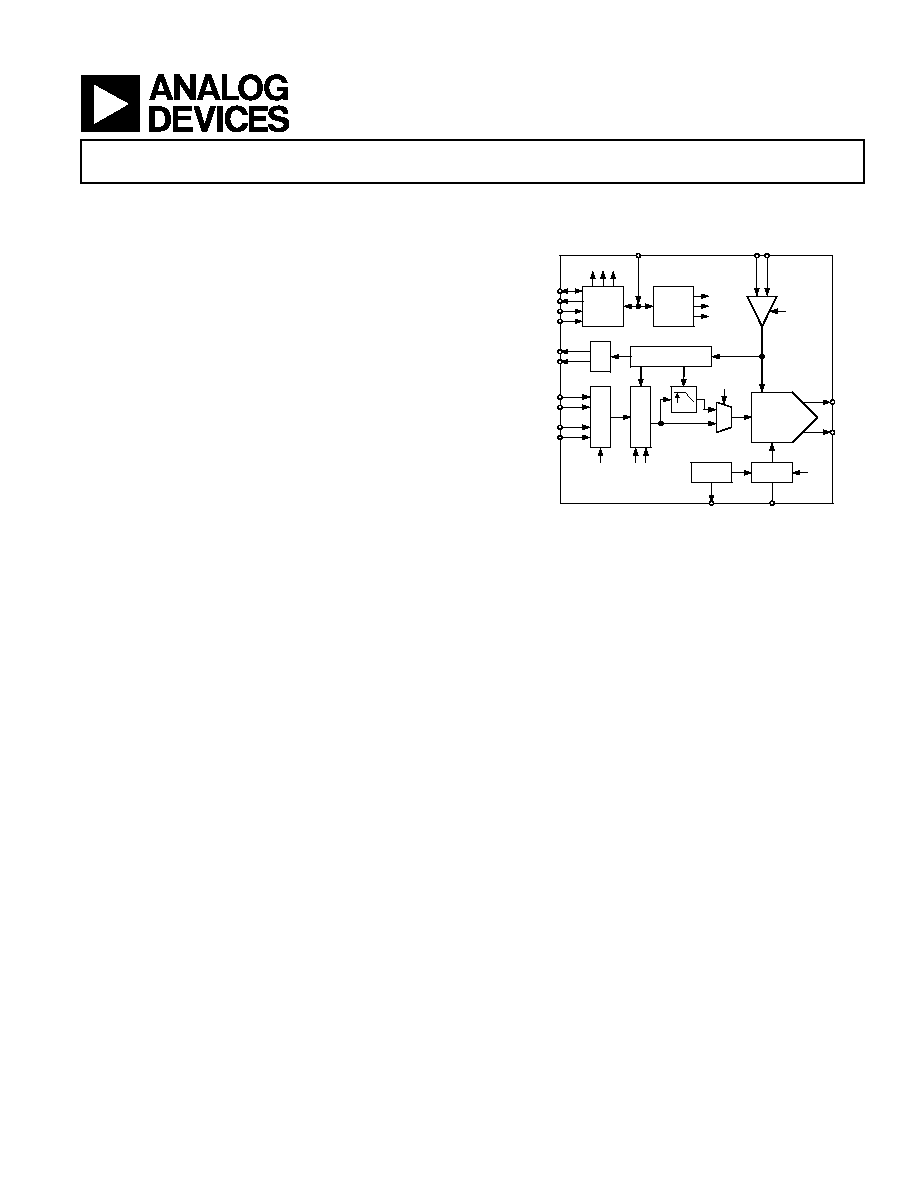
FUNCTIONAL BLOCK DIAGRAM
LV
D
S
R
e
c
e
i
v
er
S
y
n
c
hr
on
i
z
at
i
o
n
Bandgap
DATACLK_IN+
DATACLK_IN-
DB[13:0]-
DB[13:0]+
Clock Distribution
SPI
14,12,10-Bit
DAC
IOUTA
IOUTB
2X
SDO
SDI
SCLK
CSB
LV
D
S
Dr
i
v
e
r
Controller
Reference
Current
CL
K
-
CL
K
+
RS
E
T
VR
EF
RE
S
E
T
DATACLK_OUT+
DATACLK_OUT-
S1 S2 S3
C1
C2
C3
C2
C1 S1
S3
S2
C3
Figure 1. Functional Block Diagram
PRODUCT HIGHLIGHTS
Ultra-low Noise and Intermodulation Distortion (IMD) enable
high quality synthesis of wideband signals at intermediate
frequencies up to 600 MHz.
Double Data Rate (DDR) LVDS data receivers support the
maximum conversion rate of 1200 MSPS.
Direct pin programmability of basic functions or SPI port access
for complete control of all AD9736 family functions.
Manufactured on a CMOS process, the AD9736 family uses a
proprietary switching technique that enhances dynamic
performance.
The current output(s) of the AD9736 family can be easily
configured for various single-ended or differential circuit
topologies.
Rev. PrJ 9/7/2004
Information furnished by Analog Devices is believed to be accurate and reliable.
However, no responsibility is assumed by Analog Devices for its use, nor for any
infringements of patents or other rights of third parties that may result from its
use. No license is granted by implication or otherwise under any patent or patent
rights of Analog Devices. Trademarks and registered trademarks are the property
of their respective companies.
One Technology Way, P.O. Box 9106, Norwood, MA 02062-9106, U.S.A.
Tel: 781.329.4700
www.analog.com
Fax: 781.326.8703
© 2004 Analog Devices, Inc. All rights reserved.

AD9736/AD9735/AD9734
Preliminary Technical Data
Rev. PrJ | Page 2 of 42
TABLE OF CONTENTS
AD9736/AD9735/AD9734--Specifications ........................................3
DC SPECIFICATIONS ......................................................................3
DIGITAL SPECIFICATIONS............................................................4
AC SPECIFICATIONS.......................................................................5
EXPLANATION OF TEST LEVELS ................................................5
PIN FUNCTION DESCRIPTIONS......................................................6
PIN CONFIGURATION........................................................................7
PACKAGE OUTLINE.............................................................................9
Ordering Guide ...................................................................................9
TYPICAL PERFORMANCE CHARACTERISTICS........................10
SPI REGISTER MAP ............................................................................14
SPI REGISTER DESCRIPTIONS........................................................15
General Description ..............................................................................19
Serial Peripheral Interface................................................................19
AD9736 Data Interface Controllers ....................................................22
AD9736 LVDS Sample Logic...........................................................23
AD9736 SYNC Logic and Controller .............................................25
AD9736 Digital Built-In Self Test........................................................27
AD9736 Analog Control Register .......................................................28
Voltage Reference...................................................................................29
Applications Information .....................................................................30
AD9736 Evaluation Board Schematics ...............................................31
AD9736 Evaluation Board PCB Layout..............................................36
REVISION HISTORY
Revision PrA: Initial Version
Revision PrB: Updated data based on initial evaluation results
Revision PrC: Updated data for web display and ongoing evaluation results
Revision PrD: Added SPI port information
Revision PrE: Cleaned up SPI port tables, added AD9736 rev A evaluation board schematics
Revision PrF: Added BGA Package Outline Drawing
Revision PrG: Added Package Pinout
Revision PrH: Added SPI Port Description
Revision PrI: Edits for readability and clarity, Added Idd typical values and plots, Updated SPI register tables, Added LVDS and SYNC controller
sections, Added pin function table, Added BIST description, Added Analog control section, Added Vref section, Updated eval
board schematic and PCB layout
Revision PrJ: Update BIST information, Update SPI definition to include SCLK edge change for read operation, Add SPI timing, Annotate
schematic to show component values for output circuit, Update ACLR plots, Add PCB fabrication details.
Preliminary Technical Data
AD9736/AD9735/AD9734
Rev. PrJ | Page 3 of 42
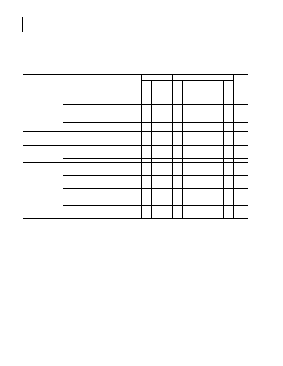
AD9736/AD9735/AD9734--SPECIFICATIONS
1
DC SPECIFICATIONS
(VDDA33 = VDDD33 = 3.3 V, VDDA18 = VDDD18 = VDDCLK = 1.8 V, MAXIMUM SAMPLE RATE, FS = 20MA,
1X MODE, 25 OHM 1% BALANCED LOAD, UNLESS OTHERWISE NOTED)
AD9736 AD9735 AD9734
Parameter Temp
Test
Level
Min Typ Max Min Typ Max Min Typ Max
Unit
RESOLUTION
14 12 10 Bits
Integral Nonlinearity (INL)
± 2.0
TBD TBD LSB
ACCURACY
Differential Nonlinearity (DNL)
± 1.0
TBD TBD LSB
Offset
Error
TBD TBD TBD %
FSR
Gain Error (With Internal Reference)
± 0.5
± 0.5
± 0.5
%
FSR
Gain Error (Without Internal Reference)
± 0.5
± 0.5
± 0.5
%
FSR
Full Scale Output Current
10
20
30
10
20
30
10
20
30
mA
Output
Compliance
Range
1.0 1.0 1.0 V
Output
Resistance
TBD TBD TBD k
ANALOG OUTPUTS
Output Capacitance
TBD TBD TBD pF
Offset
TBD TBD TBD ppm/
∞C
Gain
TBD TBD TBD ppm/
∞C
TEMPERATURE DRIFT
Reference
Voltage
TBD TBD TBD ppm/
∞C
Internal
Reference
Voltage
1.2 1.2 1.2 V
REFERENCE
Output
Current
100 100 100 nA
VDDA33
3.13 3.3 3.47 3.13 3.3 3.47 3.13 3.3 3.47 V
ANALOG SUPPLY VOLTAGES
VDDA18
1.70 1.8 1.90 1.70 1.8 1.90 1.70 1.8 1.90 V
VDDD33
3.13 3.3 3.47 3.13 3.3 3.47 3.13 3.3 3.47 V
DIGITAL SUPPLY VOLTAGES
VDDD18
1.70 1.8 1.90 1.70 1.8 1.90 1.70 1.8 1.90 V
Bypass
Mode
380 380 380 mW
FIR Interpolation Filter Enabled
550
550
550
mW
POWER CONSUMPTION
Standby
Power
TBD TBD TBD mW
IDDA33
25 TBD TBD mA
IDDA18
47 TBD TBD mA
IDDD33
10 TBD TBD mA
SUPPLY CURRENTS
1X Mode
IDDD18
122 TBD TBD mA
IDDA33
25 TBD TBD mA
IDDA18
47 TBD TBD mA
IDDD33
10 TBD TBD mA
SUPPLY CURRENTS
2x Mode, Interpoation Enabled
IDDD18
234 TBD TBD mA
Table 1: DC Specifications
1
Specifications subject to change without notice
AD9736/AD9735/AD9734
Preliminary Technical Data
Rev. PrJ | Page 4 of 42
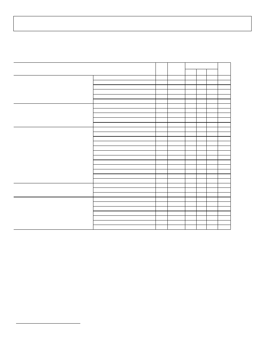
DIGITAL SPECIFICATIONS
1
(VDDA33 = VDDD33 = 3.3 V, VDDA18 = VDDD18 = VDDCLK = 1.8 V, MAXIMUM SAMPLE RATE, FS = 20MA,
1X MODE, 25 OHM 1% BALANCED LOAD, UNLESS OTHERWISE NOTED)
AD9736,35,34
Parameter Temp
Test
Level
Min Typ Max
Unit
Input voltage range, Via or Vib
825
1575
mV
Input differential threshold
-100
100
mV
Input differential hysteresis
20
mV
Receiver differential input impedance
80
120
LVDS input rate
1200
MSPS
LVDS DATA INPUTS (DB[13:0]+, DB[13:0]-)
DB+ = Via, DB- = Vib
LVDS data Bit Error Rate
TBD
Err/Bit
Input voltage range, Via or Vib
825
1575
mV
Input differential threshold
-100
100
mV
Input differential hysteresis
20
mV
Receiver differential input impedance
80
120
LVDS CLOCK INPUT (DATACLK_IN+, DATACLK_IN-)
DATACLK+ = Via, DATACLK- = Vib
Maximum Clock Rate
600
MHz
Output voltage high, Voa or Vob
1375
mV
Output voltage low, Voa or Vob
1025
mV
Output differential voltage
150
200
250
mV
Output offset voltage
1150
1250
mV
Output impedance, single ended
80
100
120
Ro mismatch between A & B
10
%
Change in |Vod| between `0' and `1'
25
mV
Change in Vos between `0' and `1'
25
mV
Output current ≠ Driver shorted to ground
20
mA
Output current ≠ Drivers shorted together
4
mA
Power-off output leakage
TBD
mA
LVDS CLOCK OUTPUT (DATACLK_OUT+, DATACLK_ OUT-)
DATACLK_OUT+ = Voa, DATACLK_OUT- = Vob
100 ohm termination
Maximum Clock Rate
600
MHz
Differential peak-to-peak Voltage
800
mV
Common Mode Voltage
400
mV
DAC CLOCK INPUT (CLK+, CLK-)
Maximum Clock Rate
1200
MHz
Maximum Clock Rate (SCLK, 1/t
SCLK
)
20
MHz
Minimum pulse width high, t
PWH
20
ns
Minimum pulse width low, t
PWL
20
ns
Minimum SDIO and CSB to SCLK setup, t
DS
10
ns
Minimum SCLK to SDIO hold, t
DH
5
ns
Maximum SCLK to valid SDIO and SDO, t
DV
20
ns
SERIAL PERIPHERAL INTERFACE
Minimum SCLK to invalid SDIO and SDO, t
DNV
5 ns
Table 2: Digital Specifications
1
LVDS Drivers and Receivers are compliant to the IEEE-1596 Reduced Range Link, unless otherwise noted
Preliminary Technical Data
AD9736/AD9735/AD9734
Rev. PrJ | Page 5 of 42
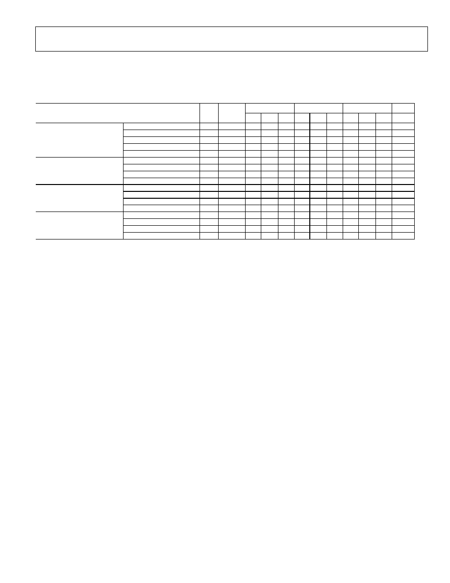
AC SPECIFICATIONS
(VDDA33 = VDDD33 = 3.3 V, VDDA18 = VDDD18 = VDDCLK = 1.8 V, MAXIMUM SAMPLE RATE, FS = 20MA,
1X MODE, 25 OHM 1% BALANCED LOAD, UNLESS OTHERWISE NOTED)
AD9736 AD9735 AD9734
Parameter Temp
Test
Level
Min Typ Max Min Typ Max Min Typ Max Unit
Maximum
Update
Rate
1200
1200
1200 MSPS
Output Settling Time (tst) (to 0.025%)
TBD
TBD
TBD
ns
Output Rise Time (10% to 90%)
TBD
TBD
TBD
ns
Output Fall Time (90% to 10%)
TBD
TBD
TBD
ns
DYNAMIC PERFORMANCE
Output
Noise
(IoutFS=20mA)
TBD TBD TBD pA/rtHz
f
DAC
= 1200 MSPS, f
OUT
= 50 MHz
80
dBc
f
DAC
= 1200 MSPS, f
OUT
= 100 MHz
77
dBc
f
DAC
= 1200 MSPS, f
OUT
= 316 MHz
63
dBc
SPURIOUS FREE DYNAMIC RANGE (SFDR)
f
DAC
= 1200 MSPS, f
OUT
= 550 MHz
55
dBc
f
DAC
= 1200 MSPS, f
OUT
= 50 MHz
85
dBc
f
DAC
= 1200 MSPS, f
OUT
= 100 MHz
84
dBc
f
DAC
= 1200 MSPS, f
OUT
= 316 MHz
74
dBc
Two Tone Intermodulation Distortion (IMD)
f
DAC
= 1200 MSPS, f
OUT
= 550 MHz
65
dBc
f
DAC
= 1200 MSPS, f
OUT
= 50 MHz
-165
dBm/Hz
f
DAC
= 1200 MSPS, f
OUT
= 100 MHz
-164
dBm/Hz
f
DAC
= 1200 MSPS, f
OUT
= 316 MHz
-158
dBm/Hz
Noise Spectral Density (NSD)
f
DAC
= 1200 MSPS, f
OUT
= 550 MHz
-155
dBm/Hz
Table 3: AC Specifications
EXPLANATION OF TEST LEVELS
TEST LEVEL
I
100% production tested.
II
100% production tested at +25∞C and guaranteed by design and characterization at specified temperatures.
III
Sample Tested Only
IV
Parameter is guaranteed by design and characterization testing.
V
Parameter is a typical value only.
VI
100% production tested at +25∞C and guaranteed by design and characterization for industrial temperature range.

AD9736/AD9735/AD9734
Preliminary Technical Data
Rev. PrJ | Page 6 of 42
PIN FUNCTION DESCRIPTIONS
Pin No.
Name
Description
A1, A2, A3, B1, B2, B3, C1, C2, C3, D2, D3
VDDC
1.8V, Clock supply
A4, A5, A6, A9, A10, A11, B4, B5, B6, B9,
B10, B11, C4, C5, C6, C9, C10, C11, D4, D5,
D6, D9, D10, D11
VSSA
Analog supply ground
A7, B7, C7, D7
IOUTB
DAC negative output, 10mA to 30mA full scale output current
A8, B8, C8, D8
IOUTA
DAC positive output, 10mA to 30mA full scale output current
A12, A13, B12, B13, C12, C13, D12, D13
VDDA
3.3V Analog supply
A14, K1
DNC
Do Not Connect
B14 I120
Nominal 1.2V reference tied to analog ground via 10kohm resistor to generate a
120uA reference current
C14 VREF
Bandgap voltage reference I/O, tie to analog ground via 1nF capacitor, output
impedance approximately 5kohms
D1, E2, E3, E4, F2, F3, F4, G1, G2, G3, G4
VSSC
Clock supply ground
D14 IPTAT
Factory test, output current proportional to absolute temperature, approximately
10uA at 25C with approximately 20nA/C slope
E1, F1
CLK-, CLK+
Negative, Positive DAC clock input (DACCLK)
E11, E12, F11, F12, G11, G12
VSSA
Analog supply ground shield
E13
IRQ / UNSIGNED
If PIN_MODE = 0, IRQ: Active low open-drain interrupt request output, pull up to
VDD3.3 with 10kohm resistor
If PIN_MODE = 1, UNSIGNED: Digital input pin where 0 = two's complement input
data format, 1 = unsigned
E14
RESET / PD
If PIN_MODE = 0, RESET: 1 resets the AD9736
If PIN_MODE = 1, PD: 1 puts the AD9736 in the power down state
F13
CSB / 2x
See SPI and PIN Mode sections for pin description
F14
SDIO / FIFO
See SPI and PIN Mode sections for pin description
G13
SCLK / FSC0
See SPI and PIN Mode sections for pin description
G14
SDO / FSC1
See SPI and PIN Mode sections for pin description
H1, H2, H3, H4, H11, H12, H13, H14, J1, J2,
J3, J4, J11, J12, J13, J14
VDD
1.8V Digital supply
K2, K3, K4, K11, K12, L2, L3, L4, L5, L6, L9,
L10, L11, L12, M3, M4, M5, M6, M9, M10,
M11, M12
VSS Digital
supply
ground
K13, K14
DB<13> -, +
Negative, Positive data input bit 13 (MSB), reduced swing LVDS
L1 PIN_MODE
0, SPI Mode, SPI enabled
1, PIN Mode, SPI disabled, direct pin control
L7, L8, M7, M8, N7, N8, P7, P8
VDD33
3.3V Digital supply
L13, L14
DB<12> -, +
Negative, Positive data input bit 12, reduced swing LVDS
M2, M1
DB<0> -, +
Negative, Positive data input bit 0 (LSB), reduced swing LVDS
M13, M14
DB<11> -, +
Negative, Positive data input bit 11, reduced swing LVDS
N1, P1
DB<1> -, +
Negative, Positive data input bit 1, reduced swing LVDS
N2, P2
DB<2> -, +
Negative, Positive data input bit 2, reduced swing LVDS
N3, P3
DB<3> -, +
Negative, Positive data input bit 3, reduced swing LVDS
N4, P4
DB<4> -, +
Negative, Positive data input bit 4, reduced swing LVDS
N5, P5
DB<5> -, +
Negative, Positive data input bit 5, reduced swing LVDS
N6, P6
DATACLK_OUT -, +
Negative, Positive output clock, reduced swing LVDS
N9, P9
DATACLK_IN -, +
Negative, Positive data input clock, reduced swing LVDS
N10, P10
DB<6> -, +
Negative, Positive data input bit 6, reduced swing LVDS
N11, P11
DB<7> -, +
Negative, Positive data input bit 7, reduced swing LVDS
N12, P12
DB<8> -, +
Negative, Positive data input bit 8, reduced swing LVDS
N13, P13
DB<9> -, +
Negative, Positive data input bit 9, reduced swing LVDS
N14, P14
DB<10> -, +
Negative, Positive data input bit 10, reduced swing LVDS
Preliminary Technical Data
AD9736/AD9735/AD9734
Rev. PrJ | Page 7 of 42
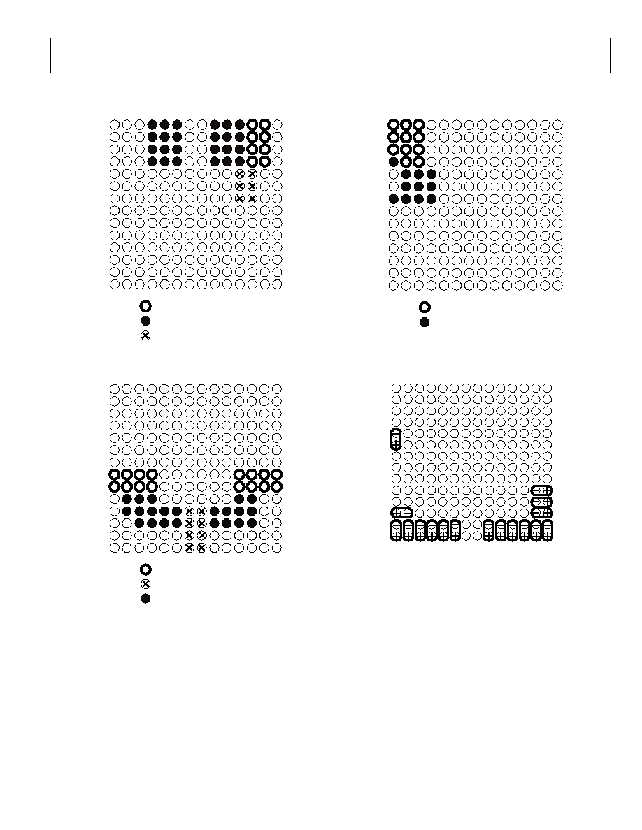
PIN CONFIGURATION
1
2
3
4
5
6
7
8
9 10 11 12 13 14
A
B
C
D
E
F
G
H
J
K
L
M
N
P
VDDA, 3.3V, Analog Supply
VSSA, Analog Supply Ground
VSSA, Analog Supply Ground Shield
Figure 2. AD9736 Analog Supply Pins (TOP view)
1
2
3
4
5
6
7
8
9 10 11 12 13 14
A
B
C
D
E
F
G
H
J
K
L
M
N
P
VDDC, 1.8V, Clock Supply
VSSC, Clock Supply Ground
Figure 3. AD9736 Clock Supply Pins (TOP view)
1
2
3
4
5
6
7
8
9 10 11 12 13 14
A
B
C
D
E
F
G
H
J
K
L
M
N
P
VDD, 1.8V Digital Supply
VSS Digital Supply Ground
VDD33, 3.3V Digital Supply
Figure 4. AD9736 Digital Supply Pins (TOP view)
1
2
3
4
5
6
7
8
9 10 11 12 13 14
A
B
C
D
E
F
G
H
J
K
L
M
N
P
LVDS13 (MS
LVDS11
LVDS12
LVDS0 (LSB)
LVDS10
LVDS6
LVDS7
LVDS8
LVDS9
LVDS5
LVDS1
LVDS
LVDS3
LVDS4
CLKP
CLKN
DCLKP,
N I
N
LVDSCLKP,
N OUT
Figure 5. AD9736 Digital LVDS Inputs, Clock I/O (TOP view)
AD9736/AD9735/AD9734
Preliminary Technical Data
Rev. PrJ | Page 8 of 42
1
2
3
4
5
6
7
8
9 10 11 12 13 14
A
B
C
D
E
F
G
H
J
K
L
M
N
P
IOUTN
IOUTP
I120
VREF
IPTAT
PIN_MODE
RESET
SDIO
SDO
IRQ
CSB
SCLK
PIN_MODE=0,
SPI ENABLED
PD
FIFO
FSC1
UNSIGNED
2x
FSCO
PIN_MODE=1,
SPI DISABLED
Figure 6. AD9736 Analog I/O and SPI Control Pins (TOP view)
Preliminary Technical Data
AD9736/AD9735/AD9734
Rev. PrJ | Page 9 of 42
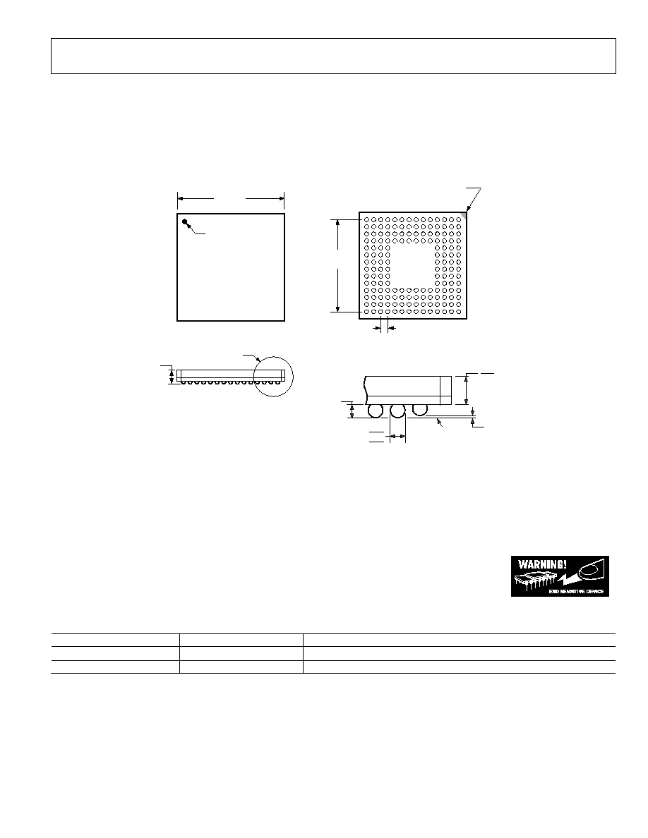
PACKAGE OUTLINE
SEATING
PLANE
0.25 MIN
DETAIL A
0.55
0.50
0.45
BALL DIAMETER
0.12 MAX
COPLANARITY
0.80 BSC
10.40
BSC
A
B
C
D
E
F
G
H
J
K
L
M
N
P
14
13
12
11
10
8
7
6
3
2
1
9
5
4
1.00
0.85
A1 CORNER
INDEX AREA
1.40 MAX
TOP VIEW
12.00
BSC SQ
BALL A1
INDICATOR
DETAIL A
COMPLIANT WITH JEDEC STANDARDS MO-205-AE.
a
160-Lead Chip Scale Ball Grid Array [CSPBGA]
(BC-160)
Dimensions shown in millimeters
BOTTOM
VIEW
Figure 7. AD9736 BGA Package Outline Drawing
ESD CAUTION
ESD (electrostatic discharge) sensitive device. Electrostatic charges as high as 4000 V readily accumulate on the
human body and test equipment and can discharge without detection. Although this product features proprietary
ESD protection circuitry, permanent damage may occur on devices subjected to high energy electrostatic discharges.
Therefore, proper ESD precautions are recommended to avoid performance degradation or loss of functionality.
Ordering Guide
Model Temperature
Range
Description
AD9736BBC
-40
∞C to +85∞C (Ambient)
160-Lead Chip Scale BGA
AD9736-EB
25∞C (Ambient)
Evaluation Board
Table 4: Ordering Guide
AD9736/AD9735/AD9734
Preliminary Technical Data
Rev. PrJ | Page 10 of 42
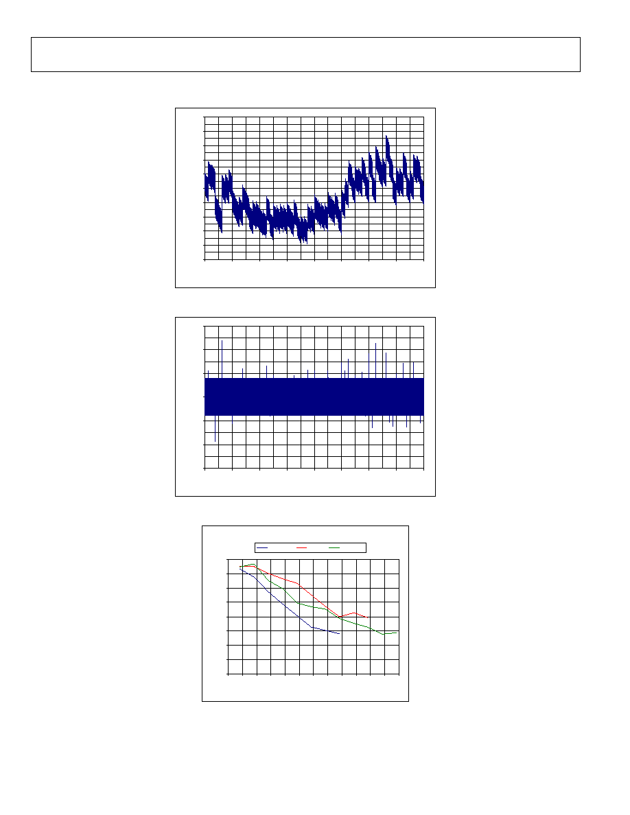
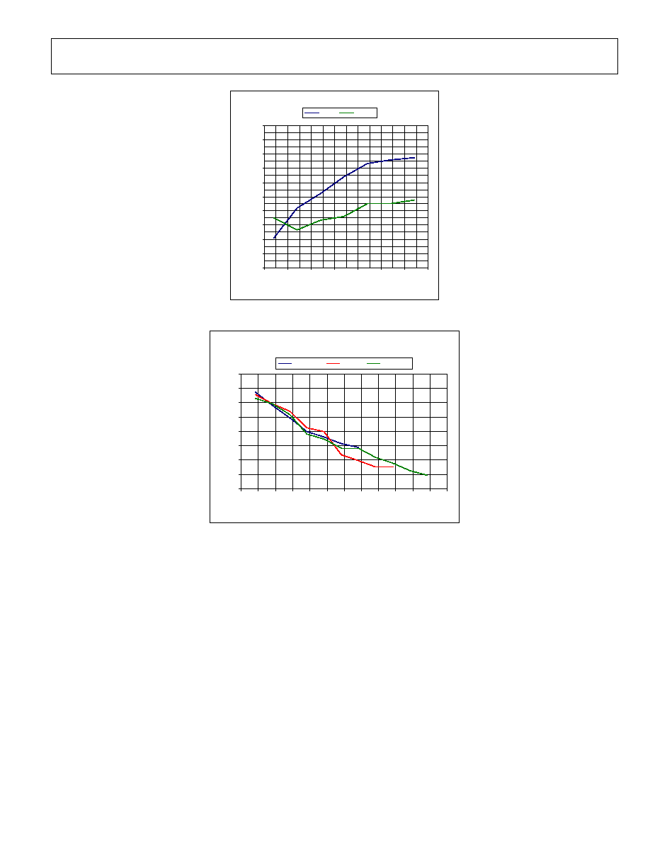
TYPICAL PERFORMANCE CHARACTERISTICS
-1
-0.8
-0.6
-0.4
-0.2
0
0.2
0.4
0.6
0.8
1
0
2048
4096
6144
8192
10240
12288
14336
16384
Code
E
rro
r -
L
S
B
Figure 8. AD9736, Typical INL
-0.7
-0.5
-0.3
-0.1
0.1
0.3
0.5
0
2048
4096
6144
8192
10240
12288
14336
16384
Code
E
rro
r -
L
S
B
Figure 9. AD9736, Typical DNL
3rd Order IMD With Respect to Fout (20mA FS)
50
55
60
65
70
75
80
85
90
0
50
100 150 200 250 300 350 400 450 500 550 600
Fout - [MHz]
I
M
D
-
[d
B
c
]
800MSPS
1GSPS
1.2GSPS
Figure 10. AD9736, 3
rd
Order IMD vs. Fout and Sample Rate
Preliminary Technical Data
AD9736/AD9735/AD9734
Rev. PrJ | Page 11 of 42
NSD Comparison With 1-Tone and 8-Tones at 1.2GSPS
-170
-168
-166
-164
-162
-160
-158
-156
-154
-152
-150
0
100
200
300
400
500
600
700
Fout - Mhz
NS
D -
d
B
m
/
Hz
1 Tone
8 Tones
Figure 11. AD9736, Noise Spectral Density (NSD) vs. Fout at 1.2GSPS
In- Band SFDR With Respect to Fout (20mA FS)
50
55
60
65
70
75
80
85
90
0
50
100 150 200 250 300 350 400 450 500 550 600
Fout - [MHz]
SF
DR -
[
d
Bc
]
800MSPS
1GSPS
1.2GSPS
Figure 12. AD9736, In Band SFDR vs. Fout and Sample Rate
AD9736/AD9735/AD9734
Preliminary Technical Data
Rev. PrJ | Page 12 of 42
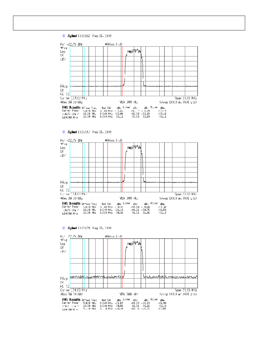
Figure 13. AD9736, WCDMA carrier at 134.83MHz, fdata=491.52MSPS
Figure 14. AD9735, WCDMA carrier at 134.83MHz, fdata=491.52MSPS
Figure 15. AD9734, WCDMA carrier at 134.83MHz, fdata=491.52MSPS
Preliminary Technical Data
AD9736/AD9735/AD9734
Rev. PrJ | Page 13 of 42
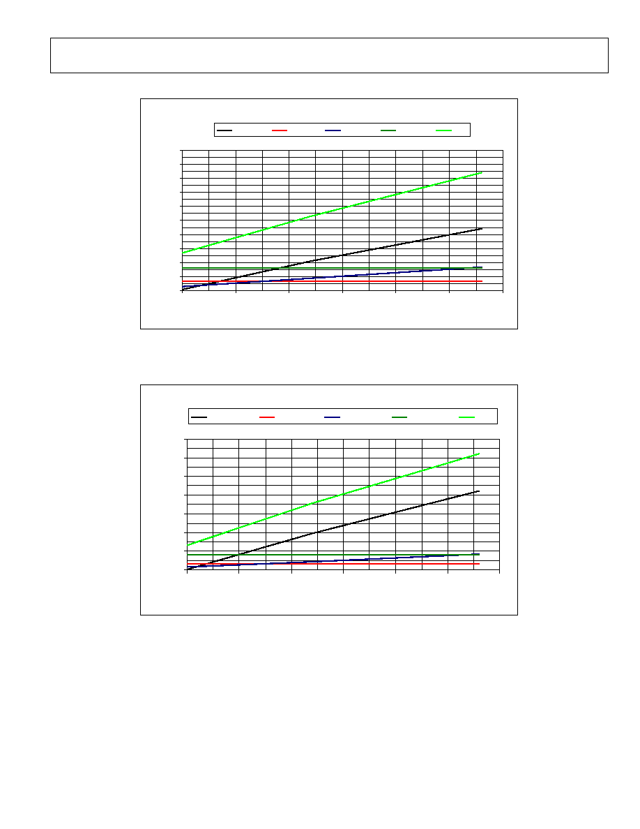
AD9736 Power Consumption 1x Mode With Respect to Clock Speed
0
0.05
0.1
0.15
0.2
0.25
0.3
0.35
0.4
0.45
0.5
0
250
500
750
1000
1250
1500
FCLK- MHz
Po
w
e
r
-
W
VDDD_1.8
VDDD_33
VDDA_1.8
VDDA_3.3
total
Figure 16. AD9736 Power vs. Clock Frequency
AD9736 Power Consumption 2x Mode With Respect to Clock Speed
0
0.1
0.2
0.3
0.4
0.5
0.6
0.7
0
250
500
750
1000
1250
1500
FCLK- MHz
Pow
e
r
-
W
VDDD_1.8
VDDD_33
VDDA_1.8
VDDA_3.3
total
Figure 17. AD9736 Power vs. Clock Frequency in 2x Mode

AD9736/AD9735/AD9734
Preliminary Technical Data
Rev. PrJ | Page 14 of 42
SPI REGISTER MAP
ADR
DEC
ADR
HEX
Register
Name
Bit 7
Bit 6
Bit 5
Bit 4
Bit 3
Bit 2
Bit 1
Bit 0
Default
(HEX)
PIN
MODE
(HEX)
0 00 MODE
SDIO_DIR LSBFIRST
RESET LONG_INS 2X
MODE FIFO
MODE
DATAFRMT
PD
00
00
1 01
IRQ
LVDS SYNC CROSS
RESV'D
IE_LVDS
IE_SYNC
IE_CROSS
RESV'D 00 00
2 02 FSC_1
SLEEP
FSC<9>
FSC<8>
02
02
3 03 FSC_2
FSC<7> FSC<6> FSC<5> FSC<4> FSC<3> FSC<2> FSC<1> FSC<0> 00 00
4 04
LVDS_CNT1
MSD<3> MSD<2> MSD<1> MSD<0> MHD<3> MHD<2> MHD<1> MHD<0> 00
00
5 05
LVDS_CNT2
SD<3> SD<2> SD<1> SD<0>
LCHANGE ERR_HI ERR_LO CHECK 00 00
6 06
LVDS_CNT3
LSURV LAUTO LFLT<3>
LFLT<2>
LFLT<1> LFLT<0> LTRH<1> LTRH<0> 00 00
7 07
SYNC_CNT1
FIFOSTAT3 FIFOSTAT2 FIFOSTAT1
FIFOSTAT0
VALID
SCHANGE PHOF<1> PHOF<0>
00
00
8 08
SYNC_CNT2
SSURV SAUTO SFLT<3>
SFLT<2>
SFLT<1>
SFLT<0> RESV'D STRH<0> 00 00
9 09 RESERVED
10 0A RESERVED
11 0B RESERVED
12 0C RESERVED
13 0D RESERVED
14 0E ANA_CNT1
MSEL<1> MSEL<0>
TRMBG<2>
TRMBG<1> TRMBG<0>
C0
C0
15 0F ANA_CNT2
HDRM<7> HDRM<6> HDRM<5>
HDRM<4>
HDRM<3>
HDRM<2> HDRM<1> HDRM<0>
CA
CA
16 10 RESERVED
17 11 BIST_CNT
SEL<1> SEL<0>
SIG_READ
LVDS_EN SYNC_EN CLEAR 00 00
18 12 BIST<7:0>
19 13 BIST<15:8>
20 14
BIST<23:16>
21 15
BIST<31:24>
22 16 CCLK_DIV
RESV'D RESV'D RESV'D RESV'D CCD<3> CCD<2> CCD<1> CCD<0> 00 00
31 1F VERSION
VER<5> VER<4> VER<3> VER<2> VER<1> VER<0> RES10
RES12
Note: Write `0' to unspecified or reserved bit locations. Reading these bits will return unknown values.
Table 5. SPI Register Map

Preliminary Technical Data
AD9736/AD9735/AD9734
Rev. PrJ | Page 15 of 42
SPI REGISTER DESCRIPTIONS
REG 00 -> MODE
Reading REG 00 returns previously written values for all defined register bits unless otherwise noted. Reset value in bold text.
ADR
Name
Bit 7
Bit 6
Bit 5
Bit 4
Bit 3
Bit 2
Bit 1
Bit 0
0x00 MODE
SDIO_DIR
LSB/MSB
RESET LONG_INS
2X
MODE
FIFO
MODE
DATAFRMT PD
SDIO_DIR
: WRITE ->
0, Input only per SPI standard
1, Bidirectional per SPI standard
LSBFIRST
: WRITE ->
0, MSB first per SPI standard
1, LSB first per SPI standard
NOTE: Only change LSB/MSB order in single byte instructions to avoid erratic behavior due to bit order errors
RESET :
WRITE->
0, Execute software reset of SPI and controllers, reload default register values EXCEPT registers 0x00 and 0x04
1, Set software reset prior to writing `0' to execute the software reset
LONG_INS :
WRITE
->
0, Short (single-byte) instruction word
1, Long (two-byte) instruction word, not necessary since the maximum internal address is REG31 (0x1F)
2X_MODE :
WRITE
->
0, Disable 2x Interpolation Filter
1, Enable 2x Interpolation Filter
FIFO_MODE :
WRITE
->
0, Disable FIFO synchronization
1, Enable FIFO synchronization
DATAFRMT :
WRITE
->
0, Signed input DATA with midscale = 0x0000
1, Unsigned input DATA with midscale = 0x2000
PD :
WRITE
->
0, Enable LVDS Receiver, DAC and Clock Circuitry
1, Power down LVDS Receiver, DAC and Clock Circuitry
REG 01 -> Interrupt Request (IRQ)
Reading REG 01 returns previously written values for all defined register bits unless otherwise noted. Reset value in bold text.
ADR
Name
Bit 7
Bit 6
Bit 5
Bit 4
Bit 3
Bit 2
Bit 1
Bit 0
0x01 IRQ
LVDS
SYNC
CROSS
RESV'D
IE_LVDS
IE_SYNC
IE_CROSS
RESV'D
LVDS
: WRITE ->
Don't Care
: READ ->
0, No active LVDS receiver interrupt
1, Interrupt in LVDS receiver occurred
SYNC
: WRITE ->
Don't Care
: READ ->
0, No active SYNC logic interrupt
1, Interrupt in SYNC logic occurred
CROSS
: WRITE ->
Don't Care
: READ ->
0, No active CROSS logic interrupt
1, Interrupt in CROSS logic occurred
IE_LVDS :
WRITE
->
0, Reset LVDS receiver interrupt and disable future LVDS receiver interrupts
1, Enable LVDS receiver interrupt to activate IRQ pin
IE_SYNC :
WRITE
->
0, Reset SYNC logic interrupt and disable future SYNC logic interrupts
1, Enable SYNC logic interrupt to activate IRQ pin
IE_CROSS :
WRITE
->
0, Reset CROSS logic interrupt and disable future CROSS logic interrupts
1, Enable CROSS logic interrupt to activate IRQ pin

AD9736/AD9735/AD9734
Preliminary Technical Data
Rev. PrJ | Page 16 of 42
REG 02, 03 -> Full Scale Current (FSC)
Reading REG 02 & 03 return previously written values for all defined register bits unless otherwise noted. Reset value in bold text.
ADR
Name
Bit 7
Bit 6
Bit 5
Bit 4
Bit 3
Bit 2
Bit 1
Bit 0
0x02
FSC_1
SLEEP
FSC<9>
FSC<8>
0x03
FSC_2
FSC<7> FSC<6> FSC<5> FSC<4> FSC<3> FSC<2> FSC<1> FSC<0>
SLEEP :
WRITE
->
0, Enable DAC output
1, Set DAC output current to 0mA
FSC<9:0>
: WRITE ->
0x000, 10mA full scale output current
0x200, 20mA full scale output current
NOTE: Iout = (72 + 192 * ( FSC<9:0> / 1024 ) ) * I120
0x3FF, 30mA full scale output current
where I120 = Vref / R120u, for example 1.2V / 10k = 120uA
REG 04, 05, 06 -> LVDS Controller (LVDS_CNT)
Reading REG 04, 05 & 06 return previously written values for all defined register bits unless otherwise noted. Reset value in bold text.
ADR
Name
Bit 7
Bit 6
Bit 5
Bit 4
Bit 3
Bit 2
Bit 1
Bit 0
0x04
LVDS_CNT1 MSD<3> MSD<2> MSD<1> MSD<0> MHD<3> MHD<2> MHD<1> MHD<0>
0x05 LVDS_CNT2 SD<3> SD<2> SD<1> SD<0>
LCHANGE
ERR_HI ERR_LO CHECK
0x06
LVDS_CNT3 LSURV LAUTO LFLT<3> LFLT<2> LFLT<1> LFLT<0> LTRH<1> LTRH<0>
MSD<3:0>
: WRITE ->
0x0, Set setup delay for the measurement system
: READ ->
If ( LAUTO == 1) the latest measured value for the setup delay
If ( LAUTO == 0) read back of the last SPI write to this bit
MHD<3:0>
: WRITE ->
0x0, Set hold delay for the measurement system
: READ ->
If ( LAUTO == 1) the latest measured value for the hold delay
If ( LAUTO == 0) read back of the last SPI write to this bit
SD<3:0>
: WRITE->
0x0, Set sample delay
: READ ->
If ( LAUTO == 1) the result of a measurement cycle is stored in this register
If ( LAUTO == 0) read back of the last SPI write to this bit
LCHANGE
: READ ->
0, No change from previous measurement
1, Change in value from the previous measurement
NOTE: The average filter and the threshold detection are not applied to this bit
ERR_HI
: READ ->
One of the 15 LVDS inputs is above the input voltage limits of the IEEE reduce link spec.
ERR_LO
: READ ->
One of the 15 LVDS inputs is below the input voltage limits of the IEEE reduced link spec.
CHECK
: READ ->
0, Phase measurement ≠ sampling in the previous or following DATA cycle
1, Phase measurement ≠ sampling in the correct DATA cycle
LSURV :
WRITE
->
0, The controller stops after completion of the current measurement cycle
1, Continuous measurements are taken and an interrupt is issued if the clock alignment drifts beyond the threshold value
LAUTO :
WRITE
->
0, Sample delay is not automatically updated
1, Continuously starts measurement cycles and updates the sample delay according to the measurement
NOTE: LSURV (REG06 Bit 7) must be set to 1 and the LVDS IRQ (REG01 Bit 3) must be set to 0 for AUTO mode
LFLT<3:0> :
WRITE
->
0x0, Average filter length, Delay = Delay + Delta Delay / 2^ LFLT<3:0>, values greater than 12 (0x0C) are clipped to 12

Preliminary Technical Data
AD9736/AD9735/AD9734
Rev. PrJ | Page 17 of 42
LTRH<2:0> :
: WRITE ->
000, Set auto update threshold values
REG 07, 08 -> SYNC Controller (SYNC_CNT)
Reading REG 07 & 08 return previously written values for all defined register bits unless otherwise noted. Reset value in bold text.
ADR
Name
Bit 7
Bit 6
Bit 5
Bit 4
Bit 3
Bit 2
Bit 1
Bit 0
0x07
SYNC_CNT1 FIFOSTAT3 FIFOSTAT2 FIFOSTAT1 FIFOSTAT0
VALID
SCHANGE PHOF<1> PHOF<0>
0x08
SYNC_CNT2 SSURV SAUTO SFLT<3> SFLT<2> SFLT<1> SFLT<0> RESV'D STRH<0>
FIFOSTAT<2:0>
: READ ->
Position of FIFO read counter, range from 0 to 7
FIFOSTAT<3>
: READ ->
0, SYNC logic OK
1, Error in SYNC logic
VALID
: READ ->
0, FIFOSTAT<3:0> is not valid yet
1, FIFOSTAT<3:0> is valid after a reset
SCHANGE
: READ ->
0, No change in FIFOSTAT<3:0>
1, FIFOSTAT<3:0> has changed since the previous measurement cycle when SSURV = 1 (surveillance mode active)
PHOF<1:0> :
WRITE
->
00, Change the readout counter
: READ ->
Current setting of the readout counter (PHOF<1:0>) in surveillance mode (SSURV = 1) after an interrupt
Current calculated optimal readout counter value in AUTO mode (SAUTO = 1)
SSURV :
WRITE
->
0, The controller stops after completion of the current measurement cycle
1, Continuous measurements are taken and an interrupt is issued if the readout counter drifts beyond the threshold value
SAUTO :
WRITE
->
0, Readout counter (PHOF<3:0>) is not automatically updated
1, Continuously starts measurement cycles and updates the readout counter according to the measurement
NOTE: SSURV (REG08 Bit 7) must be set to 1 and the SYNC IRQ (REG01 Bit 2) must be set to 0 for AUTO mode
SFLT<3:0> :
WRITE
->
0x0, Average filter length, FIFOSTAT = FIFOSTAT + Delta FIFOSTAT / 2 ^ SFLT<3:0>, values greater than 12 (0x0C) are clipped to 12
STRH<0> :
WRITE
->
0, If FIFOSTAT<2:0> = 0 | 7, generate a SYNC interrupt
1, If FIFOSTAT<2:0> = 0 | 1 | 6 | 7, generate a SYNC interrupt
REG 14, 15 -> Analog Control (ANA_CNT)
Reading REG 14 & 15 return previously written values for all defined register bits unless otherwise noted. Reset value in bold text.
ADR
Name
Bit 7
Bit 6
Bit 5
Bit 4
Bit 3
Bit 2
Bit 1
Bit 0
0x0E ANA_CNT1
MSEL<1>
MSEL<0>
TRMBG<2>
TRMBG<1>
TRMBG<0>
0x0F
ANA_CNT2 HDRM<7> HDRM<6> HDRM<5> HDRM<4> HDRM<3> HDRM<2> HDRM<1> HDRM<0>
MSEL<1:0> :
WRITE
->
00, Mirror roll off frequency control = bypass
01, Mirror roll off frequency control = narrowest bandwidth
10, Mirror roll off frequency control = medium bandwidth
11, Mirror roll off frequency control = widest bandwidth
NOTE: See plot in the applications section
TRMBG<2:0>
: WRITE ->
000, Bandgap temperature characteristic trim
NOTE: See plot in the applications section
HDRM<7:0>
: WRITE ->
0xCA, Output stack headroom control
HDRM<7:4> set reference offset from Vdd3v (vcas centering)
HDRM<3:0> set overdrive (current density) trim (temperature tracking)
Note: Set to 0xCA for optimum performance

AD9736/AD9735/AD9734
Preliminary Technical Data
Rev. PrJ | Page 18 of 42
REG 17, 18, 19, 20, 21 -> Built-in Self Test Control (BIST_CNT)
Reading REG17, 18, 19, 20 & 21 return previously written values for all defined register bits unless otherwise noted. Reset value in bold text.
ADR
Name
Bit 7
Bit 6
Bit 5
Bit 4
Bit 3
Bit 2
Bit 1
Bit 0
0x11 BIST_CNT
SEL<1>
SEL<0>
SIG_READ
LVDS_EN
SYNC_EN
CLEAR
0x12
BIST<7:0> BIST<7> BIST<6> BIST<5> BIST<4> BIST<3> BIST<2> BIST<1> BIST<0>
0x13
BIST<15:8> BIST<15> BIST<14> BIST<13> BIST<12> BIST<11> BIST<10> BIST<9> BIST<8>
0x14
BIST<23:16> BIST<23> BIST<22> BIST<21> BIST<20> BIST<19> BIST<18> BIST<17> BIST<16>
0x15
BIST<31:24> BIST<31> BIST<30> BIST<29> BIST<28> BIST<27> BIST<26> BIST<25> BIST<24>
SEL<1:0>
: WRITE ->
00, Write result of the LVDS Phase 1 BIST to BIST<31:0>
01, Write result of the LVDS Phase 2 BIST to BIST<31:0>
10, Write result of the SYNC Phase 1 BIST to BIST<31:0>
11, Write result of the SYNC Phase 2 BIST to BIST<31:0>
SIG_READ
: WRITE ->
0, No action
1, Enable BIST signature readback
LVDS_EN :
WRITE->
0, No action
1, Enable LVDS BIST
SYNC_EN :
WRITE
->
0, No Action
1, Enable SYNC BIST
CLEAR :
WRITE
->
0, No Action
1, Clear all BIST registers
BIST<31:0>
: READ ->
Results of the Built-in Self Test
REG 22 -> Controller Clock Pre-divider (CCLK_DIV)
Reading REG 22 returns previously written values for all defined register bits unless otherwise noted. Reset value in bold text.
ADR
Name
Bit 7
Bit 6
Bit 5
Bit 4
Bit 3
Bit 2
Bit 1
Bit 0
0x16
CCLK_DIV RESV'D RESV'D RESV'D RESV'D CCD<3>
CCD<2>
CCD<1>
CCD<0>
CCD<3:0> :
WRITE
->
0x0, Controller Clock = DACCLK / 16
0x1, Controller Clock = DACCLK / 32
0x2, Controller Clock = DACCLK / 64 ...
0xF, Controller Clock = DACCLK / 524288
NOTE: The 100MHz to 1.2GHz DACCLK must be divided to less than 10MHz for correct operation. CCD<3:0> must be programmed to
divide the DACCLK so that this relationship is not violated. Controller Clock = DACCLK / ( 2 ^ ( CCD<3:0> + 4 ))
REG 31 -> VERSION
Reading REG 31 returns previously written values for all defined register bits unless otherwise noted. Reset value in bold text.
ADR
Name
Bit 7
Bit 6
Bit 5
Bit 4
Bit 3
Bit 2
Bit 1
Bit 0
0x1F
VERSION VER<5> VER<4> VER<3> VER<2> VER<1> VER<0> RES10 RES12
VER<5:0>
: READ ->
Version number (part ID), 00001, Revision 1, initial release
RES10 (msb)
RES12 (lsb)
: READ ->
00, 14-bit DAC
01, 12-bit DAC
10, 10-bit DAC
Preliminary Technical Data
AD9736/AD9735/AD9734
Rev. PrJ | Page 19 of 42
GENERAL DESCRIPTION
The AD9736/35/34 are 14/12/10-bit DACs which run at an update
rate up to 1.2GSPS. Input data can be accepted up to the full
1.2GSPS rate or a 2x interpolation filter may be enabled (2x mode)
allowing full-speed operation with a 600MSPS input data rate.
DATA and DATACLK_IN inputs are parallel LVDS meeting the
IEEE reduced swing LVDS specifications with the exception of
input hysteresis. The DATACLK_IN input runs at one half the
input DATA rate in a double data rate (DDR) format. Each edge of
DATACLK_IN is used to transfer DATA into the AD9736 as shown
in Figure 25.
The DACCLK (pins E1, F1) directly drives the DAC core to
minimize clock jitter. It is also divided by two (1x and 2x mode)
then output as the DATACLK_OUT. The DATACLK_OUT signal
is used to clock the data source. The DAC expects DDR LVDS data
(DB<13:0>) aligned with the DDR input clock (DATACLK_IN)
from a circuit similar to the one shown in Figure 35. Clock
relationships are shown in Table 6.
MODE DACCLK
DATACLK
OUT
DATACLK
IN
DATA
1x 1.2GHz
600MHz
600MHz
1.2GSPS
2x 1.2GHz
600MHz
300MHz
600MSPS
Table 6. AD9736 Clock Relationships
Maintaining correct alignment of data and clock is a common
challenge with high-speed DACs, complicated by changes in
temperature and other operating conditions. The AD9736
simplifies this high-speed data capture problem with two adaptive
closed-loop timing controllers.
One timing controller manages the LVDS data and data clock
alignment (LVDS controller) and the other manages the LVDS data
and DACCLK alignment (SYNC controller). The LVDS controller
locates the data transitions and delays the DATACLK_IN so that its
transition is in the center of the valid data window. The SYNC
controller manages the FIFO that moves data from the LVDS
DATACLK_IN domain to the DACCLK domain. Both controllers
can be operated in manual mode under external processor control,
surveillance mode where error conditions generate external
interrupts or automatic mode where errors are automatically
corrected.
The LVDS and SYNC controllers include moving average filtering
for noise immunity and variable thresholds to control their activity.
Normally the controllers can be set to run in automatic mode and
they will make any necessary adjustments without dropping or
duplicating samples sent to the DAC. Both controllers require
initial calibration prior to entering automatic update mode.
Control of the AD9736 functions is via the serially programmed
registers listed in Table 5.
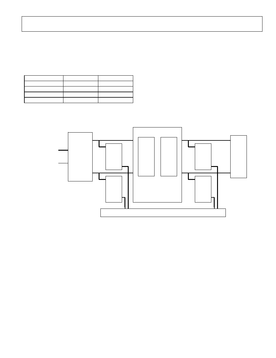
Serial Peripheral Interface
The AD9736 serial port is a flexible, synchronous serial
communications port allowing easy interface to many industry-
standard microcontrollers and microprocessors. The serial I/O is
compatible with most synchronous transfer formats, including both
the Motorola SPIÆ and IntelÆ SSR protocols. The interface allows
read/write access to all registers that configure the AD9736. Single
or multiple byte transfers are supported, as well as MSB first or LSB
first transfer formats. The AD9736's serial interface port can be
configured as a single pin I/O (SDIO) or two unidirectional pins for
in/out (SDIO/SDO).
Figure 18. AD9736 SPI Port
The AD9736 may optionally be configured via external pins rather
than the serial interface. When the PIN_MODE input (pin L1) is
high the serial interface is disabled and its pins are reassigned for
direct control of the DAC. Specific functionality is described in the
PIN Mode section.
GENERAL OPERATION OF THE SERIAL INTERFACE
There are two phases to a communication cycle with the AD9736.
Phase 1 is the instruction cycle, which is the writing of an
instruction byte into the AD9736, coincident with the first eight
SCLK rising edges. The instruction byte provides the AD9736 serial
port controller with information regarding the data transfer cycle,
which is Phase 2 of the communication cycle. The Phase 1
instruction byte defines whether the upcoming data transfer is read
or write, the number of bytes in the data transfer, and the starting
register address for the first byte of the data transfer. The first eight
SCLK rising edges of each communication cycle are used to write
the instruction byte into the AD9736.
The remaining SCLK edges are for Phase 2 of the communication
cycle. Phase 2 is the actual data transfer between the AD9736 and
the system controller. Phase 2 of the communication cycle is a
transfer of 1, 2, 3, or 4 data bytes as determined by the instruction
byte. Using one multibyte transfer is the preferred method. Single
byte data transfers are useful to reduce CPU overhead when
register access requires one byte only. Registers change immediately
upon writing to the last bit of each transfer byte.
CSB can be raised after each sequence of 8 bits (except the last byte)
to stall the bus. The serial transfer will resume when CSB is
lowered. Stalling on non-byte boundaries will reset the SPI.
SDO (Pin G14)
SDIO (Pin F14)
SCLK (Pin G13)
CSB (Pin F13)
AD9736
SPI Port
AD9736/AD9735/AD9734
Preliminary Technical Data
Rev. PrJ | Page 20 of 42
SHORT INSTRUCTION MODE (8-BIT INSTRUCTION)
The short instruction byte is shown in Table 7.
MSB
LSB
I7 I6 I5 I4 I3 I2 I1 I0
R/W N1 N0 A4 A3 A2 A1 A0
Table 7. SPI Instruction Byte
R/W
, Bit 7 of the instruction byte, determines whether a read or a
write data transfer will occur after the instruction byte write. Logic
high indicates read operation. Logic 0 indicates a write operation.
N1, N0
, Bits 6 and 5 of the instruction byte, determine the number
of bytes to be transferred during the data transfer cycle. The bit
decodes are shown in Table 8.
A4, A3, A2, A1, A0
, Bits 4, 3, 2, 1, 0 of the instruction byte,
determine which register is accessed during the data transfer
portion of the communications cycle. For multibyte transfers, this
address is the starting byte address. The remaining register
addresses are generated by the AD9736 based on the LSBFIRST bit
(REG00, bit 6).
N1
N2
Description
0
0
Transfer 1 Byte
0
1
Transfer 2 Bytes
1
0
Transfer 3 Bytes
1
1
Transfer 4 Bytes
Table 8. Byte Transfer Count
LONG INSTRUCTION MODE (16-BIT INSTRUCTION)
The long instruction bytes are shown in Table 7.
MSB
LSB
I15 I14 I13 I12 I11 I10 I9 I8
R/W N1 N0 A12 A11 A10 A9 A8
I7 I6 I5 I4 I3 I2 I1 I0
A7 A6 A5 A4 A3 A2 A1 A0
Table 9. SPI Instruction Byte
If LONG_INS = 1 (REG00, bit 4) the instruction byte is extended to
two bytes where the second byte provides an additional 8 bits of
address information. Addresses 0x00 ≠ 0x1F are equivalent in short
and long instruction modes. The AD9736 does not use any
addresses greater than 31 (0x1F) so always set LONG_INS = 0.
SERIAL INTERFACE PORT PIN DESCRIPTIONS
SCLK--Serial Clock
. The serial clock pin is used to synchronize
data to and from the AD9736 and to run the internal state
machines. SCLK's maximum frequency is 20 MHz. All data input
to the AD9736 is registered on the rising edge of SCLK. All data is
driven out of the AD9736 on the rising edge of SCLK.
CSB--Chip Select
. Active low input starts and gates a
communication cycle. It allows more than one device to be used on
the same serial communications lines. The SDO and SDIO pins will
go to a high impedance state when this input is high. Chip select
should stay low during the entire communication cycle.
SDIO--Serial Data I/O
. Data is always written into the AD9736 on
this pin. However, this pin can be used as a bidirectional data line.
The configuration of this pin is controlled by SDIO_DIR at REG00,
bit 7. The default is Logic 0, which configures the SDIO pin as
unidirectional.
SDO--Serial Data Out
. Data is read from this pin for protocols
that use separate lines for transmitting and receiving data. In the
case where the AD9736 operates in a single bidirectional I/O mode,
this pin does not output data and is set to a high impedance stat
e.
MSB/LSB TRANSFERS
The AD9736 serial port can support both most significant bit
(MSB) first or least significant bit (LSB) first data formats. This
functionality is controlled by LSBFIRST at REG00, bit 6. The
default is MSB first (LSBFIRST = 0).
When LSBFIRST = 0 (MSB first) the instruction and data bytes
must be written from most significant bit to least significant bit.
Multibyte data transfers in MSB first format start with an
instruction byte that includes the register address of the most
significant data byte. Subsequent data bytes should follow in order
from high address to low address. In MSB first mode, the serial
port internal byte address generator decrements for each data byte
of the multibyte communication cycle.
When LSBFIRST = 1 (LSB first) the instruction and data bytes
must be written from least significant bit to most significant bit.
Multibyte data transfers in LSB first format start with an
instruction byte that includes the register address of the least
significant data byte followed by multiple data bytes. The serial port
internal byte address generator increments for each byte of the
multibyte communication cycle.
The AD9736 serial port controller data address will decrement
from the data address written toward 0x00 for multibyte I/O
operations if the MSB first mode is active. The serial port controller
address will increment from the data address written toward 0x1F
for multibyte I/O operations if the LSB first mode is active.
NOTES ON SERIAL PORT OPERATION
The AD9736 serial port configuration is controlled by REG00, bits
4, 5, 6 and 7. It is important to note that the configuration changes
immediately upon writing to the last bit of the register. For
multibyte transfers, writing to this register may occur during the
middle of communication cycle. Care must be taken to compensate
for this new configuration for the remaining bytes of the current
communication cycle. The same considerations apply to setting the
software reset, RESET (REG00, bit 5). All registers are set to their
default values EXCEPT REG00 and REG04 which remain
unchanged.
Use of only single byte transfers when changing serial port
Preliminary Technical Data
AD9736/AD9735/AD9734
Rev. PrJ | Page 21 of 42
configurations or initiating a software reset is highly
recommended. In the event of unexpected programming sequences
the AD9736 SPI may become inaccessible. For example, if user
code inadvertently changes the LONG_INS bit or LSBFIRST bit the
following bits may have unexpected results. The SPI can be
returned to a known state by writing an incomplete byte (1-7 bits)
of all zeroes followed by three bytes of 0x00. This will return to
MSB first short instructions (REG00 = 0x00) so the device may be
reinitialized.
R/W N0 N1 A0 A1
A2 A3 A4 D7 D6
N
D5
N
D0
0
D1
0
D2
0
D3
0
D7 D6
N
D5
N
D0
0
D1
0
D2
0
D3
0
INSTRUCTION CYCLE
DATA TRANSFER CYCLE
CSB
SCLK
SDIO
SDO
Figure 19. Serial Register Interface Timing MSB First
INSTRUCTION CYCLE
DATA TRANSFER CYCLE
CSB
SCLK
SDIO
SDO
A0 A1 A2 A3 A4
N1 N0 R/W D0D1
0
D2
0
D7
N
D6
N
D5
N
D4
N
D0D1
0
D2
0
D7
N
D6
N
D5
N
D4
N
Figure 20. Serial Register Interface Timing LSB First
INSTRUCTION BIT 6
INSTRUCTION BIT 7
CSB
SCLK
SDIO
t
DS
t
DS
t
DH
t
PWH
t
PWL
t
SCLK
03152-P
r
D
-
006
Figure 21. Timing Diagram for SPI Register Write
I1
I0
D7
D6
D5
t
DV
t
DNV
CSB
SCLK
SDIO
Figure 22. Timing Diagram for SPI Register Read
After the last instruction bit is written to the SDIO pin the driving
signal must be set to a high impedance in time for the bus to turn
around. The serial output data from the AD9736 will be enabled by
the falling edge of SCLK. This causes the first output data bit to be
shorter than the remaining data bits as shown in Figure 22.
PIN MODE OPERATION
When the PIN_MODE input (pin L1) is set high, the SPI port is
disabled. The SPI port pins are remapped as shown in Table 10. The
function of these pins is described in Table 11. The remaining
PIN_MODE register settings are shown in Table 5, the SPI register
map.
Pin Number
PIN_MODE = 0
PIN_MODE = 1
E13 IRQ
UNSIGNED
F13 CSB 2X
G13 SCLK FSC0
E14 RESET PD
F14 SDIO FIFO
G14 SDO FSC1
Table 10. SPI_MODE vs. PIN_MODE Inputs
Pin Function
UNSIGNED
0, Two's complement input data format
1, Unsigned input data format
2X
0, Interpolation disabled
1, Interpolation = 2x enabled
FSC1, FSC0
00, Sleep mode
01, 10mA full scale output current
10, 20mA full scale output current
11, 30mA full scale output current
PD
0, Chip enabled
1, Chip in power down state
FIFO
0, Input FIFO disabled
1, Input FIFO enabled
Table 11. PIN_MODE Input Functions
Care must be taken when using PIN_MODE since only the control
bits shown in Table 11 can be changed. If the remaining register
default values are not suitable for the desired operation
PIN_MODE cannot be used.
AD9736/AD9735/AD9734
Preliminary Technical Data
Rev. PrJ | Page 22 of 42
AD9736 DATA INTERFACE CONTROLLERS
There are 2 internal controllers that can be utilized in the operation
of the AD9736. The first controller helps maintain optimum LVDS
data sampling and the second controller helps maintain optimum
synchronization between the DACCLK and the incoming data. The
LVDS controller is responsible for optimizing the sampling of the
data from the LVDS bus (DB13:0) while the SYNC controller
resolves timing problems between the DAC_CLK (CLK+, CLK-)
and the DATACLK. A block diagram of these controllers is shown
in Figure 23.
The controllers are clocked with a divided down version of the
DAC_CLK. The divide ratio is set utilizing the controller clock
predivider bits (CCD<3:0>) located at REG22 bits 3:0 to generate
the controller clock as follows:
Controller Clock = DAC_CLK / ( 2 ^ ( CCD<3 :0> + 4 ))
NOTE
: The controller clock may not exceed 10MHz for correct
operation. Until CCD<3:0> has been properly programmed to
meet this requirement the DAC output may not be stable.
The LVDS and SYNC controllers can be independently operated in
3 different modes via SPI port REG06 and REG08.
1.
Manual Mode
2.
Surveillance Mode
3.
Auto Mode
In manual mode all of the timing measurements and updates are
externally controlled via the SPI.
In surveillance mode each controller takes measurements and
calculates a new "optimal" value continuously. The result of the
measurement can be passed through an averaging filter before
evaluating the results for increased noise immunity. The filtered
result is compared to a threshold value set via REG06 and REG08
of the SPI port. If the error is greater then the threshold, an
interrupt is triggered and the controller stops. REG01 of the SPI
port controls the interrupts with bits 3 and 2 enabling the
respective interrupts and bits 7 and 6 indicating the respective
controller's interrupt. If an interrupt is enabled it will also activate
the AD9736's IRQ pin. In order to clear an interrupt the interrupt
enable bit of the respective controller must be set to a zero for at
least one controller clock cycle (controller clock < 10MHz).
Auto mode is almost identical to surveillance mode. Instead of
triggering an interrupt and stopping the controller, the controller
automatically updates its settings to the newly calculated "optimal"
value and continues to run.
Figure 23.AD9736 Internal Synchronization Engine
Data Source
i.e. FPGA
LVDS
SAMPLE
LOGIC
FIFO
SYNC
LOGIC
DAC
DACCLK
DATACLK_OUT
DB<13:0>
DATACLK_IN
CLK Control
LVDS
Controller
SYNC
Controller
Data Source
i.e. FPGA
LVDS
SAMPLE
LOGIC
FIFO
SYNC
LOGIC
DAC
DACCLK
DATACLK_OUT
DB<13:0>
DATACLK_IN
CLK Control
LVDS
Controller
SYNC
Controller
Preliminary Technical Data
AD9736/AD9735/AD9734
Rev. PrJ | Page 23 of 42
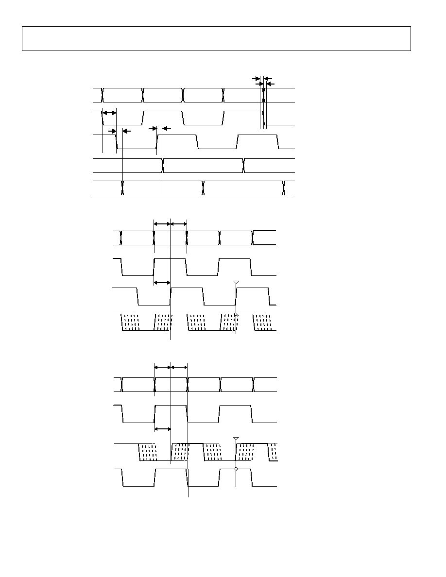
AD9736 LVDS Sample Logic
A simplified diagram of the AD9736 LVDS data sampling engine is
shown in Figure 24, with the timing relationships shown in Figure
25.
The incoming LVDS data is latched by the DATA SAMPLING
SIGNAL (DSS) which is derived from DATACLK_IN. The LVDS
controller delays DATACLK_IN to create the DATA SAMPLING
SIGNAL (DSS) which is adjusted to sample the LVDS data in the
center of the valid data window. The skew between the
DATACLK_IN and the LVDS data bits (DB<13:0>) must be
minimal (t1 and t2 in Figure 25) for proper operation. Therefore, it
is recommended that the DATACLK_IN be generated in the same
manner as the LVDS data bits (DB<13:0>) with the same driver and
data lines (i.e. it should just be another LVDS data bit running a
constant 01010101... sequence, as shown in Figure 35).
Figure 24. AD9736 Internal LVDS Data Sampling Logic
LVDS SAMPLE LOGIC CALIBRATION
The internal DATA SAMPLING SIGNAL delay must be calibrated
to optimize the data sample timing. Once calibrated, the AD9736
can generate an IRQ or automatically correct its timing if
temperature or voltage variations change the timing too much. This
calibration is done by using the delayed CLOCK SAMPLING
SIGNAL (CSS) to sample the DELAYED CLOCK SIGNAL (DCS).
The LVDS sampling logic can find the edges of the DATACLK_IN
signal and from this measurement the center of the valid data
window can be located.
The internal delay line which derives the delayed DATA
SAMPLING SIGNAL (DSS) from DATACLK_IN is controlled by
SD3:0 (REG05, bits 7:4) while the DELAYED CLOCK SIGNAL
(DCS) is controlled by MSD3:0 (REG04, bits 7:4) and the CLOCK
SAMPLING SIGNAL (CSS) is controlled by MHD3:0 (REG04, bits
3:0).
DATACLK_IN transitions must be time aligned with the LVDS
data (DB<13:0>) transitions. This allows the CLOCK SAMPLING
SIGNAL (CSS, derived from the DATACLK_IN), to find the valid
data window of DB<13:0> by locating the DATACLK_IN edges.
The latching (rising) edge of CSS is initially placed using bits
SD<3:0> and can then be shifted to the left using MSD<3:0> and to
the right using MHD<3:0>. When CSS samples the DELAYED
CLOCK SIGNAL (DCS) and the result is a 1, (which can be read
back via the CHECK bit at REG05, bit 0) then the sampling is
occurring in the correct data cycle. In order to find the leading
edge of the data cycle, increment MSD (Measured Set-up Delay)
until CHECK goes low. In order to find the trailing edge, increment
MHD (Measured Hold Delay) until CHECK goes low. Always set
MHD = 0 when incrementing MSD and vice-versa.
Note:
The incremental units of SD, MSD, and MHD are in units of
real time, not fractions of a clock cycle. At this time, the delay from
each increment of these bits has not been fully characterized. Over
process, voltage, and temperature, each increment may introduce
between 25 and 100ps of delay with a nominal target of 80ps.
OPERATING THE LVDS CONTROLLER IN MANUAL
MODE VIA THE SPI PORT
The manual operation of the LVDS controller allows the user to
step through both the set-up and hold delays to calculate the
optimal sampling delay (i.e. center of the data eye).
With SD<3:0> and MHD<3:0> set to zero, increment the set-up
time delay (MSD<3:0>, REG04, bits 7:4) until the check bit
(REG05, bit 0) goes low and record this value. This locates the
leading DATACLK_IN (and DATA) transition as shown in Figure
26.
With SD<3:0> and MSD<3:0> set to zero, increment the hold time
delay (MHD<3:0>, REG04, bits 3:0) until the check bit (REG05 bit
0) goes low and record this value. This locates the trailing
DATACLK_IN (and DATA) transition as shown in Figure 27.
Once both DATACLK_IN edges are located the Sample Delay
(SD<3:0>, REG05, bits 7:4) must be updated according to the
following equation:
Sample Delay = ( MHD ≠ MSD ) / 2
After updating SD<3:0>, verify that the sampling signal is in the
middle of the valid data window by adjusting both MHD then
MSD with the new sample delay until the CHECK bit goes low. The
new MHD and MSD values should be equal or within one unit
delay if SD<3:0> was set correctly.
NOTE
: The Sample Delay calibration just described should be
performed prior to enabling Surveillance mode or Auto mode.
LVDS
RX
LVDS
RX
FF
SD<3:0>
Sample Delay
FF
D1
D2
DB<13:0>
DATACLK
IN
DATA SAMPLING
SIGNAL
FF
MSD<3:0>
Delay
MHD<3:0>
Delay
CHECK
CLOCK
SAMPLING
SIGNAL
DELAYED
CLOCK
SIGNAL
AD9736/AD9735/AD9734
Preliminary Technical Data
Rev. PrJ | Page 24 of 42
Figure 25. AD9736 Internal LVDS Data Sampling Logic Timing
Figure 26. Set-Up Delay Measurement
Figure 27. Hold Delay Measurement
DB13:0
DATACLK_IN
DATA
SAMPLING
SIGNAL
D1
D2
t1
t2
SAMPLE
DELAY
PROP DELAY
TO LATCH
PROP DELAY
TO LATCH
DB<13:0>
DATACLK_IN
CSS with
MHD<3:0> = 0
DCS, delayed
by MSD<3:0>
MSD<3:0> = 0 1 2 3 4 5
set up time (ts)
hold time (th)
CHECK = 1 1 1 1 1 0
Sample Delay , SD<3:0>
CSS Samples DCS
CHECK = 1
DB<13:0>
DATACLK_IN
DCS with
MSD<3:0> = 0
MHD<3:0> = 0 1 2 3 4 5
CHECK = 1 1 1 1 1 0
set up time (ts)
hold time (th)
Sample Delay, SD<3:0>
CSS Samples DCS
CSS, delayed
by MHD<3:0>
CHECK = 1

Preliminary Technical Data
AD9736/AD9735/AD9734
Rev. PrJ | Page 25 of 42
OPERATING THE LVDS CONTROLLER IN SURVEILLANCE
AND AUTO MODE
In surveillance mode, the controller searches for the edges of the
data eye in the same manner as above in the manual mode of
operation and triggers an interrupt if the CLOCK SAMPLING
SIGNAL (CSS) has moved more than the threshold value set by
LTHR<1:0> (REG06, bits 1:0).
There is an internal filter which averages the set-up and hold time
measurements to filter out noise and glitches on the clock lines.
Average Value = ( MHD ≠ MSD ) / 2
New Average = Average Value + ( Delta Average / 2 ^ LFLT<3:0> )
If an accumulating error in the Average Value causes it to exceed
the Threshold value (LTHR<1:0>) an interrupt will be issued.
The maximum allowable value for LFLT<3:0> is 12.
In surveillance mode, the ideal sampling point should first be
found using manual mode and applied to the sample delay
registers. The user should then set the threshold and filter values
depending on how far the CSS signal is allowed to drift before an
interrupt occurs. Then set the surveillance bit high (REG06, bit 7)
and monitor the interrupt signal either via the SPI port read back
(REG01, bit 3) or the IRQ pin.
In auto mode, the same steps should be taken to set up the sample
delay, threshold and filter length. In order to run the controller in
auto mode both the LAUTO (REG06, bit 6) and LSURV (REG06,
bit 7) bits need to be set to 1. In AUTO mode the LVDS interrupt
should be set low (REG01, bit 7) to allow the Sample Delay to be
automatically updated if the threshold value is exceeded.
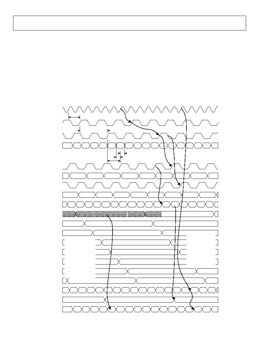
AD9736 SYNC Logic and
Controller
A FIFO structure is utilized to synchronize the data transfer
between the DACCLK and the DATACLK_IN clock domains. The
SYNC Controller writes data from DB<13:0> into an eight word
memory based on a cyclic write counter clocked by the CLOCK
SAMPLING SIGNAL (CSS) which is a delayed version of
DACCLK_IN. The data is read out of the memory based on a
second cyclic read counter clocked by DACCLK. The eight word
deep FIFO shown in Figure 28 provides sufficient margin to
maintain proper timing under most conditions. The SYNC logic is
designed to prevent the read and write pointers from crossing. If
the timing drifts far enough to require an update of the phase offset
(PHOF<1:0>) two samples will be duplicated or dropped. Figure 29
shows the timing diagram for the SYNC logic.
SYNC LOGIC AND CONTROLLER OPERATION
The relationship between the readout pointer and the write pointer
will initially be unknown since the startup relationship between
DACCLK and DATACLK_IN is unknown. The SYNC logic
measures the relative phase between the two counters with the zero
detect block and the Flip Flop in Figure 5 above. The relative phase
is returned in FIFOSTAT<2:0> (REG07, bits 6:4) and SYNC logic
errors are indicated by FIFOSTAT<3> (REG07, bit 7). If
FIFOSTAT<2:0> returns a value of zero or seven it signifies that the
memory is sampling in a critical state (read and write pointers are
close to crossing). If the FIFOSTAT<2:0> returns a value of 3 or 4 it
signifies the memory is sampling at the optimal state (read and
write pointers are farthest apart). If FIFOSTAT<2:0> returns a
critical value the pointer can be adjusted with the phase offset
PHOF<1:0> (REG07, bits 1:0). Due to the architecture of the FIFO
the phase offset can only adjust the read pointer in steps of two.
OPERATING IN MANUAL MODE
Allow DACCLK and DATACLK_IN to stabilize then enable FIFO
mode (REG00, bit 2). Read FIFOSTAT<2:0> (REG07, bits 6:4) to
determine if adjustment is needed. For example if FIFOSTAT<2:0>
= 6 the timing is not yet critical but it is not optimal. To return to
an optimal state (FIFOSTAT<2:0> = 4) the PHOF<1:0> (REG07,
bits 1:0) needs to be set to 1. Setting PHOF<1:0> = 1 effectively
increments the read pointer by 2. This causes the write pointer
value to be captured two clocks later decreasing FIFOSTAT<2:0>
from 6 to 4.
Figure 28. SYNC Logic Block Diagram
8 Word
Memory
DAC<13:0>
DB<13:0>
M0
M7
Write
Counter
Read
Counter
Adder
CSS
DACCLK
PHOF<1:0>
ZD
FF
FF
FIFOSTAT<2:0>
8 Word
Memory
DAC<13:0>
DB<13:0>
M0
M7
Write
Counter
Read
Counter
Adder
CSS
DACCLK
PHOF<1:0>
ZD
FF
FF
FIFOSTAT<2:0>
AD9736/AD9735/AD9734
Preliminary Technical Data
Rev. PrJ | Page 26 of 42
OPERATION IN SURVEILLANCE AND AUTO MODES
Once FIFOSTAT<2:0> has been manually placed in an optimal
state the AD9736 SYNC logic can be run in Surveillance or Auto
mode. To start, turn on Surveillance mode by setting SSURV = 1
(REG08, bit 7) then enable the sync interrupt (REG01, bit 2). If
STRH<0> = 0 (REG08, bit 0) an interrupt will occur if
FIFOSTAT<2:0> = 0 or 7. If STRH<0> = 1 (REG08, bit 0) an
interrupt will occur if FIFOSTAT<2:0> = 0, 1, 6 or 7. The interrupt
can be read at REG01, bit 6 at the AD9736 IRQ pin.
To enter Auto mode, complete the preceding steps then set SAUTO
= 1 (REG09, bit 6). Next set the SYNC interrupt = 0 (REG01, bit 2),
to allow the phase offset (PHOF<1:0>) to be automatically updated
if FIFOSTAT<2:0> violates the threshold value.
The FIFOSTAT signal is filtered to improve noise immunity and
reduce unnecessary phase offset updates. The filter operates with
the following algorithm:
FIFOSTAT = FIFOSTAT + Delta FIFOSTAT / 2 ^ SFLT<3:0>
Where 0 <= SFLT<3:0> <= 12. Values greater than 12 are set to 12.
SAMPLE_HOLD
SAMPLE_SETUP
SAMPLE_DELAY
EXTERNAL_DELAY
INTERNAL_DELAY
B
C
D
E
F
G
H
I
J
K
M
O
L
N
P
R
Q
A
A
B
C
D
E
F
G
H
I
J
K
L
M
N
O
P
Q
0
1
2
3
4
5
6
7
0
1
2
3
A
C
E
G
I
K
M
4
5
6
7
0
1
2
3
4
5
6
7
4
0
4
4
4
A
B
C
D
E
F
G
H
I
J
K
L
M
5
6
7
0
1
B
D
F
H
J
L
1
2
3
4
DACCLK
DATACLK_OUT
DATACLK_IN
DATA_IN
CSS1
D1
CSS2
D2
WRITE_PTR1
M0
M1
M2
M3
M4
M5
M6
M7
READ_PTR1
FIFOSTAT
DAC_DATA
Figure 29. SYNC Logic Timing Diagram
Safe Zone
Error Zone
Data `A' can be
safely read from
the FIFO in the
Safe Zone. In
the Error Zone,
the pointers
may briefly
overlap due to
clock jitter or
FIFOSTAT is set
equal to the
write pointer
each time the
read pointer
changes from 7
to 0.
Preliminary Technical Data
AD9736/AD9735/AD9734
Rev. PrJ | Page 27 of 42
AD9736 DIGITAL BUILT-IN SELF TEST
BIST may be used to validate data transfer to the AD9736 in
addition to final ATE device verification. There are 4 BIST
signatures that can be read back using Registers 18-21 based on the
setting of the BIST selection bits (REG17, bits 7:6) as shown in
Table 12.
SEL<1> SEL<0>
1 - LVDS Phase 1
0
0
2 - LVDS Phase 2
0
1
3 - SYNC Phase 1
1
0
4 - SYNC Phase 2
1
1
Table 12. BIST Selection Bits
The BIST signature returned from the AD9736 will depend on the
input DATA during the test. Since the filters in the DAC have
memory, it is important to put the correct idle value on the DATA
inputs to flush the memory prior to reading the BIST signature.
Placing the idle value on the data inputs also allows the BIST to be
setup while the DAC clock is running. The idle value should be all
zeroes in unsigned mode (0x0000) and all zeroes except for the
MSB in two's complement mode (0x2000).
The BIST consists of two stages; the first stage is after the LVDS
receiver and the second stage is after the FIFO stage. The first BIST
stage verifies correct sampling of the data from the LVDS bus while
the second BIST stage verifies correct synchronization between the
DAC_CLK domain and the DATA_CLK domain. The BIST vector
is generated using 32 bit LFSR signature logic. Since the internal
architecture is a two bus parallel system there are two 32-bit LFSR
signature logic blocks on the both the LVDS and SYNC blocks.
Figure 30 shows where the LVDS and SYNC phases are located.
Figure 30. Block Diagram Showing LVDS and SYNC Phase 1 and Phase 2
BIST OPERATION
The internal signature generator processes the input data to create
the BIST signatures. An external program which implements the
same algorithm may be used to generate the expected signature for
comparison. A Matlab routine can be provided upon request to
perform this function.
Clock the test vector in as described below and compare the
signature register values to the expected value to verify correct
operation and input data capture.
With all clocks running:
1.
Apply the idle vector to the data inputs (0x0000 if
unsigned, 0x2000 if two's complement) for 1024 clocks,
2.
Set LVDS_EN (REG17, bit 2) and SYNC_EN (REG17, bit
1) high,
3.
Set CLEAR (REG17, bit 0) high,
4.
Set CLEAR low to clear the BIST signature register,
5.
Clock the BIST vector into the LVDS data inputs,
6.
After the BIST vector is complete, return the inputs to the
idle vector value,
7.
Set LVDS_EN (REG17, bit 2) and SYNC_EN (REG17, bit
1) low,
8.
Set the desired SEL<1:0> bits and read back the four
BIST signature registers (REG18, 19, 20 and 21).
When the DAC is in 1x mode, the signature at SYNC BIST, Phase 1
should equal the signature at LVDS BIST, Phase 1. The same is
true for Phase 2. BIST does not support 2x mode.
LVDS
RX
Figure 24
DB<13:0>
DATACLK_IN
LVDS
BIST
PH1
LVDS
BIST
PH2
SYNC
BIST
PH1
SYNC
BIST
PH2
SYNC Logic
DAC
SPI Port
D1
D2
FIFO 2x
AD9736/AD9735/AD9734
Preliminary Technical Data
Rev. PrJ | Page 28 of 42
AD9736 ANALOG CONTROL REGISTER
The AD9736 includes some registers for optimizing its analog
performance. These registers include temperature trim for the
bandgap, noise reduction in the output current mirror and output
current mirror headroom adjustments.
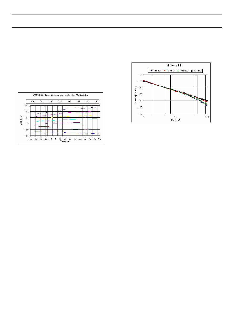
BANDGAP TEMPERATURE CHARACTERISTIC TRIM BITS
Using TRMBG<2:0> (REG14, bits 2:0) the temperature
characteristic of the internal bandgap can be trimmed to minimize
the drift over temperature as shown in Figure 31.
Figure 31. BANDGAP Temperature Characteristic for Various TRMBG Values
It is important to note that the temperature changes are sensitive to
process variations and the above plot may not be representative of
all fabrication lots. Optimum adjustment requires measurement of
the device operation at two temperatures and development of a
trim algorithm to program the correct TRMBG<2:0> values in
external non-volatile memory.
MIRROR ROLL OFF FREQUENCY CONTROL
With MSEL<1:0> (REG14, bits 7:6) the user can adjust the noise
contribution of the internal current mirror to optimize the 1/F
noise. Figure 32 shows MSEL vs. the 1/F noise with 20mA Full-
Scale current into a 50ohm resistor.
Figure 32. 1/F Noise With Respect to MSEL Bits
HEADROOM BITS
HDRM<7:0> (REG15, bits 7:0) is for internal evaluation and it is
not recommended to change them from their default reset values.
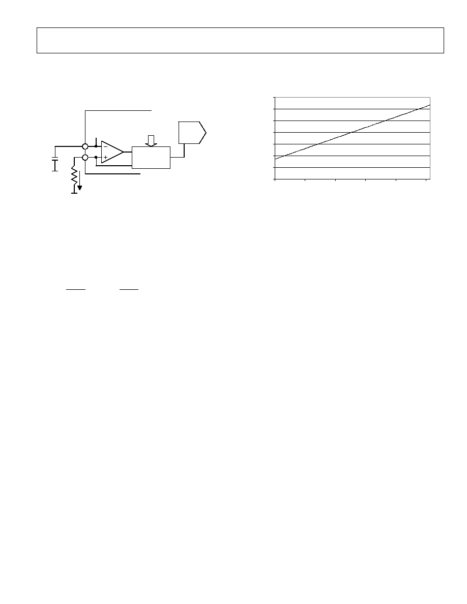
Preliminary Technical Data
AD9736/AD9735/AD9734
Rev. PrJ | Page 29 of 42
VOLTAGE REFERENCE
The AD9736 output current is set by a combination of digital
control bits and the I120 reference current as shown in Figure 33.
Figure 33. Voltage Reference Circuit
The reference current is obtained by forcing the bandgap voltage
across an external 10kohm resistor from I120 (pin B14) to ground.
The 1.2V nominal bandgap voltage (Vref) will generate a 120uA
reference current in the 10k resistor. This current is adjusted
digitally by FSC<9:0> (REG02, REG03) to set the output full scale
current I
FS
:
>
<
◊
+
◊
=
0
:
9
1024
192
2
7
R
Vref
FSC
I
FS
The full scale output current range is 10mA to 30mA for register
values from 0x000 to 0x3FF. The default value of 0x200 generates
20mA full scale. The typical range is shown in
Figure 34
.
0
5
10
15
20
25
30
35
0
200
400
600
800
1000
DAC gain code
I
FS
(m
a
)
Figure 34. I
FS
vs. DAC Gain Code
VREF (pin C14) must be bypassed to ground with a 1nF capacitor.
The bandgap voltage is present on this pin and may be buffered for
use in external circuitry. The typical output impedance is near
5kohms. If desired, an external reference may be used to overdrive
the internal reference by connecting it to the VREF pin.
IPTAT (pin D14) is used for factory testing. It may be left floating
(preferred) or tied to analog ground. It will output a current which
is proportional to absolute temperature. The nominal output is
approximately 10uA at 25C. The slope is approximately 20nA per
degree C.
Current
Scaling
DAC
Vbg
1.2V
FSC<9:0>
Ifull-scale
AD9736
I120
1nF
Vref
I120
10k
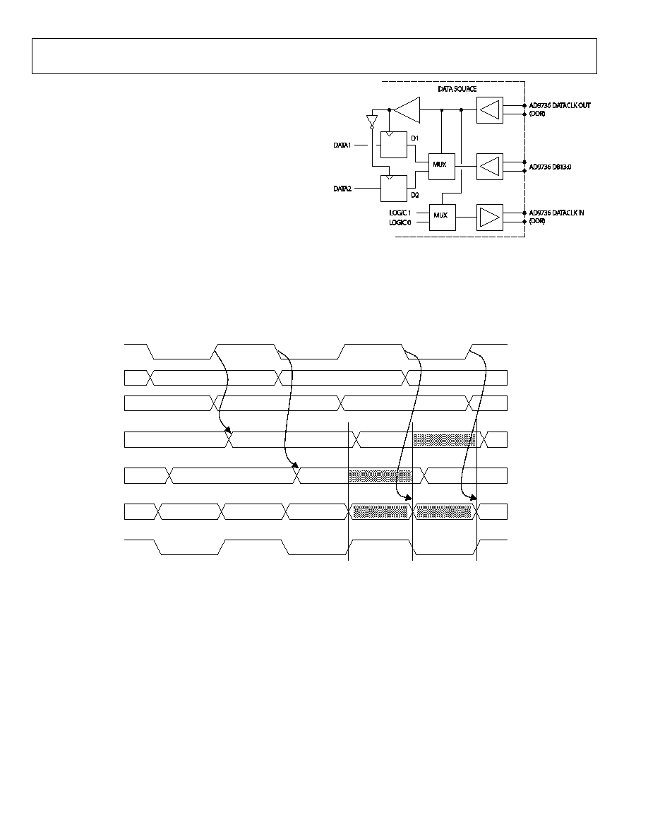
AD9736/AD9735/AD9734
Preliminary Technical Data
Rev. PrJ | Page 30 of 42
APPLICATIONS INFORMATION
FPGA/ASIC DAC DRIVER REQUIREMENTS
To achieve data synchronization using the high speed capability of
the AD9736, ADI recommends the configuration in Figure 35 for
the FPGA/ASIC driving the digital inputs. Using the Double Data
Rate DATACLK_OUT, this configuration will generate the LVDS
DATACLK_IN to drive the AD9736 at the DDR rate. The circuit
also synchronizes the DATACLK_IN and the digital input data
(DB<13:0>) as required by the AD9736. The synchronization
engine in the AD9736 then uses DATACLK_IN to generate the
internal CLOCK SAMPLING SIGNAL to capture the incoming
data via the Manual, Surveillance or Auto mode.
To operate in 2x mode, the circuit in Figure 35 must be modified to
include a divide-by-two block in the DATACLK_OUT path.
Without this additional divider the DATA and DATACLK_IN will
be running 2x too fast. DATACLK_OUT is always DACCLK/2.
Figure 35. Recommended FPGA/ASIC Configuration for Driving AD9736
Digital Inputs, 1x Mode
Figure 36. FPGA/ASIC Timing for Driving AD9736 Digital Inputs, 1x Mode
TIMING ERROR BUDGET
The following components make up the timing error budget for the
AD9736:
1.
AD9736 DATACLK_OUT jitter
2.
AD9736 DATACLK_IN jitter
3.
DB13:0 jitter
4.
DB13:0 skew from data source
5.
DB13:0 receiver skew margin (board + AD9736 internal
delays)
6.
DB13:0 to DATACLK_IN skew from data source
A
C
E
B
D
A
C
B
D
A
B
C
DATACLK_OUT+
DATA1
DATA2
D1
D2
DB
DATACLK_IN+
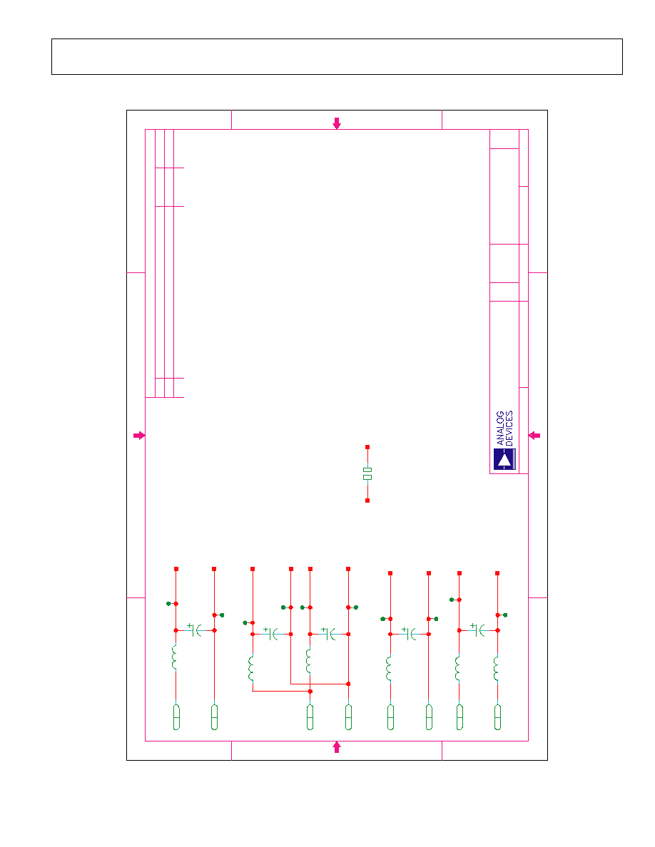
Preliminary Technical Data
AD9736/AD9735/AD9734
Rev. PrJ | Page 31 of 42
AD9736 EVALUATION BOARD SCHEMATICS
0
1
2
1
C
L
0
1
2
1
C
L
E
S
A
C
A
E
S
A
C
A
E
S
A
C
A
E
S
A
C
A
E
S
A
C
A
1
B
N
E
G
O
R
D
Y
H
F
0
T
E
E
R
T
S
N
R
U
B
O
W
4
0
8
G
N
I
R
U
T
C
A
F
U
N
A
M
N
O
T
G
N
I
M
L
I
W
E
L
A
C
S
T
O
N
O
D
E
L
A
C
S
V
E
R
R
E
B
M
U
N
G
N
I
W
A
R
D
O
N
M
C
S
F
E
Z
I
S
E
N
O
N
D
E
V
O
R
P
P
A
E
T
A
D
S
N
O
I
S
I
V
E
R
N
O
I
T
P
I
R
C
S
E
D
V
E
R
1
D
C
B
A
1
2
3
4
A
B
C
D
2
3
4
7
8
8
1
0
A
M
,
N
O
T
G
N
I
M
L
I
W
:
Y
B
D
E
V
O
R
P
P
A
:
Y
B
N
W
A
R
D
T
E
E
H
S
M
R
J
8
2
.
8
0
3
0
.
b
v
e
r
a
g
b
c
a
d
a
g
i
g
m
o
r
f
a
t
a
d
e
c
r
u
o
S
A
0
1
2
1
C
L
0
1
2
1
C
L
0
1
2
1
C
L
0
1
2
1
C
L
A
S
S
V
A
S
S
V
S
S
V
S
S
V
T
U
D
R
E
D
N
U
S
R
E
T
L
I
F
T
U
P
N
I
R
E
W
O
P
9
1
.
5
0
4
0
=
E
T
A
D
E
L
I
F
A
N
A
8
1
A
N
A
3
3
G
I
D
8
1
S
S
V
G
I
D
3
3
E
T
I
R
R
E
F
7
L
A
8
1
D
D
V
B
8
1
D
D
V
3
3
D
D
V
3
3
A
D
D
V
A
S
S
V
E
T
I
R
R
E
F
1
L
E
T
I
R
R
E
F
4
L
E
T
I
R
R
E
F
3
L
A
S
S
V
1
1
P
T
K
L
B
C
D
D
V
C
5
A
S
S
V
1
P
J
S
S
V
3
1
P
T
K
L
B
K
L
B
4
1
P
T
3
P
T
K
L
B
4
P
T
D
E
R
5
P
T
K
L
B
D
E
R
6
P
T
1
P
T
D
E
R
2
2
C
F
U
0
1
V
3
.
6
8
1
C
F
U
0
1
V
3
.
6
4
1
C
F
U
0
1
V
3
.
6
0
1
C
F
U
0
1
V
3
.
6
1
C
F
U
0
1
V
3
.
6
E
T
I
R
R
E
F
6
L
E
T
I
R
R
E
F
5
L
1
1
B
T
4
2
B
T
3
2
B
T
2
2
B
T
1
2
B
T
4
1
B
T
3
1
B
T
2
1
B
T
D
E
R
7
P
T
D
E
R
9
P
T
S
S
V
S
S
V
Figure 37. Power Supply Inputs for AD9736 Evaluation Board, Rev C
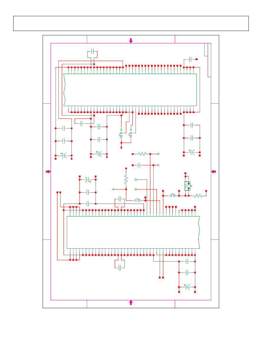
AD9736/AD9735/AD9734
Preliminary Technical Data
Rev. PrJ | Page 32 of 42
B
A
3
0
6
0
C
C
3
0
6
0
C
C
3
0
6
0
C
C
E
S
A
C
A
3
0
6
0
C
C
3
0
6
0
C
C
E
S
A
C
A
3
0
6
0
C
C
3
0
6
0
C
C
E
S
A
C
A
E
S
A
C
A
3
0
6
0
C
C
E
S
A
C
A
3
0
6
0
C
C
3
0
6
0
C
C
RC1206
3
0
6
0
C
C
3
0
6
0
C
C
3
0
6
0
C
C
3
0
6
0
C
C
3
0
6
0
C
C
3
0
6
0
C
C
N
E
G
O
R
D
Y
H
2
3
3
A
S
S
V
1
3
3
A
S
S
V
4
3
3
A
S
S
V
5
3
3
A
D
D
V
6
3
3
A
D
D
V
7
1
3
3
A
S
S
V
6
1
3
3
A
S
S
V
1
2
3
3
A
S
S
V
0
2
3
3
A
S
S
V
2
N
I
P
K
L
C
N
K
L
C
2
1
3
3
A
S
S
V
1
1
3
3
A
S
S
V
0
1
3
3
A
S
S
V
9
3
3
A
S
S
V
8
3
3
A
S
S
V
7
3
3
A
S
S
V
1
C
S
S
V
1
1
C
D
D
V
8
C
D
D
V
7
C
D
D
V
5
C
D
D
V
4
C
D
D
V
3
C
D
D
V
B
S
C
_
X
2
O
I
D
S
_
O
F
I
F
9
C
S
S
V
8
C
S
S
V
5
C
S
S
V
4
C
S
S
V
3
C
S
S
V
2
C
S
S
V
K
L
C
S
_
0
C
S
F
O
D
S
_
1
C
S
F
1
D
L
E
I
H
S
2
D
L
E
I
H
S
5
D
L
E
I
H
S
6
D
L
E
I
H
S
1
1
C
S
S
V
0
1
C
S
S
V
7
3
3
A
D
D
V
8
3
3
A
D
D
V
0
2
1
I
E
R
A
P
S
T
A
T
P
I
4
3
3
A
D
D
V
2
3
3
A
D
D
V
4
2
3
3
A
S
S
V
3
1
3
3
A
S
S
V
3
P
I
3
N
I
2
C
D
D
V
0
1
C
D
D
V
7
C
S
S
V
4
D
L
E
I
H
S
T
E
S
E
R
_
D
P
3
3
3
A
D
D
V
1
3
3
A
D
D
V
3
2
3
3
A
S
S
V
2
2
3
3
A
S
S
V
9
1
3
3
A
S
S
V
8
1
3
3
A
S
S
V
5
1
3
3
A
S
S
V
4
P
I
4
N
I
3
3
3
A
S
S
V
5
3
3
A
S
S
V
1
C
D
D
V
9
C
D
D
V
6
C
S
S
V
3
D
L
E
I
H
S
Q
R
I
_
D
E
N
G
I
S
1
P
I
2
P
I
F
E
R
V
6
3
3
A
S
S
V
6
C
D
D
V
4
1
3
3
A
S
S
V
1
N
I
P
O
T
N
E
G
O
R
D
Y
H
6
D
D
V
5
D
D
V
8
D
D
V
N
2
1
S
D
V
L
P
2
1
S
D
V
L
0
2
S
S
V
9
D
D
V
6
1
S
S
V
7
1
S
S
V
2
D
D
V
8
S
S
V
4
S
S
V
3
S
S
V
P
2
S
D
V
L
N
2
S
D
V
L
P
0
S
D
V
L
N
0
S
D
V
L
E
D
O
M
_
I
P
S
2
2
S
S
V
1
K
C
N
1
2
S
S
V
N
7
S
D
V
L
P
7
S
D
V
L
P
5
S
D
V
L
N
5
S
D
V
L
P
4
S
D
V
L
N
4
S
D
V
L
N
6
S
D
V
L
P
6
S
D
V
L
N
N
I
K
L
C
S
D
V
L
P
N
I
K
L
C
S
D
V
L
6
3
3
D
D
V
5
3
3
D
D
V
4
3
3
D
D
V
3
3
3
D
D
V
P
1
1
S
D
V
L
P
0
1
S
D
V
L
N
0
1
S
D
V
L
P
9
S
D
V
L
P
3
1
S
D
V
L
1
1
S
S
V
3
1
S
S
V
2
1
D
D
V
3
D
D
V
2
S
S
V
0
1
S
S
V
P
1
S
D
V
L
P
T
U
O
K
L
C
S
D
V
L
7
3
3
D
D
V
P
8
S
D
V
L
N
3
1
S
D
V
L
2
1
S
S
V
4
1
S
S
V
5
1
S
S
V
8
1
S
S
V
9
1
S
S
V
0
1
D
D
V
1
1
D
D
V
4
D
D
V
1
S
S
V
9
S
S
V
N
1
S
D
V
L
N
T
U
O
K
L
C
S
D
V
L
8
3
3
D
D
V
N
8
S
D
V
L
6
1
D
D
V
1
D
D
V
N
9
S
D
V
L
7
D
D
V
5
S
S
V
7
S
S
V
6
S
S
V
4
1
D
D
V
5
1
D
D
V
3
1
D
D
V
1
3
3
D
D
V
2
3
3
D
D
V
N
3
S
D
V
L
P
3
S
D
V
L
N
1
1
S
D
V
L
M
O
T
T
O
B
2
V
E
R
1
D
C
B
A
1
2
3
4
A
B
C
D
2
3
4
F
O
B
A
3
0
6
0
C
R
Q
R
I
A
_
T
E
S
E
R
T
E
S
E
R
JP3
3
3
A
D
D
V
Q
R
I
3
3
D
D
V
3
3
D
D
V
K
0
1
6
1
R
T
H
W
2
P
T
3
3
D
D
V
3
1
2
8
P
J
JP4
A
S
S
V
5
N
E
G
O
R
D
Y
H
C
2
J
1
J
4
J
3
1
L
4
1
L
1
1
K
1
1
J
1
1
L
0
1
L
2
H
4
M
4
L
3
L
2
P
2
N
1
M
2
M
1
L
2
L
1
K
2
K
1
1
N
1
1
P
5
P
5
N
4
P
4
N
0
1
N
0
1
P
9
N
9
P
8
N
8
P
7
P
7
N
4
1
M
4
1
P
4
1
N
3
1
P
4
1
K
2
1
M
0
1
M
4
1
J
3
H
4
K
6
M
1
P
6
P
8
M
2
1
P
3
1
K
1
1
M
9
M
2
1
L
9
L
2
1
K
2
1
J
3
1
J
4
H
3
K
5
M
1
N
6
N
8
L
2
1
N
4
1
H
1
H
3
1
N
3
J
5
L
3
M
6
L
2
1
H
3
1
H
1
1
H
7
L
7
M
3
N
3
P
3
1
M
1
U
5
A
4
A
4
B
2
1
C
3
1
C
0
1
B
9
B
1
1
C
0
1
C
7
B
1
F
1
E
6
D
5
D
4
D
6
C
5
C
4
C
1
D
3
D
2
C
1
C
2
B
1
B
3
A
3
1
F
4
1
F
2
G
1
G
2
F
4
E
3
E
2
E
3
1
G
4
1
G
1
1
E
2
1
E
1
1
G
2
1
G
4
G
3
G
2
1
D
3
1
D
4
1
B
4
1
A
4
1
D
3
1
B
3
1
A
1
1
D
9
A
8
C
7
C
2
A
2
D
4
F
2
1
F
4
1
E
2
1
B
2
1
A
0
1
D
9
D
9
C
1
1
B
1
1
A
8
D
7
D
6
A
5
B
1
A
3
C
3
F
1
1
F
3
1
E
8
A
8
B
4
1
C
6
B
3
B
0
1
A
7
A
1
U
T
A
T
P
I
2
1
P
T
T
H
W
F
N
1
9
C
%
1
.
K
0
0
.
0
1
1
R
S
S
V
7
C
P
N
D
A
8
1
D
D
V
P
N
D
8
C
6
C
P
N
D
P
N
D
5
C
3
C
F
U
1
.
0
T
H
W
0
1
P
T
0
2
1
I
T
H
W
8
P
T
F
E
R
V
N
I
P
K
L
C
D
S
S
V
5
R
K
0
1
3
1
C
F
N
1
4
C
F
N
1
A
S
S
V
1
1
C
F
U
7
.
4
V
3
.
6
2
1
C
F
U
1
.
0
2
C
F
U
7
.
4
V
3
.
6
1
3
2
4
1
W
S
5
;
S
S
V
5
1
C
F
U
7
.
4
V
3
.
6
6
1
C
F
U
1
.
0
7
1
C
F
N
1
3
2
C
F
U
7
.
4
V
3
.
6
4
2
C
F
U
1
.
0
5
2
C
F
N
1
9
1
C
F
U
7
.
4
V
3
.
6
0
2
C
F
U
1
.
0
1
2
C
F
N
1
N
3
1
B
D
P
3
1
B
D
N
2
1
B
D
P
2
1
B
D
N
1
1
B
D
P
1
1
B
D
N
0
1
B
D
P
0
1
B
D
N
9
B
D
P
9
B
D
N
8
B
D
P
8
B
D
T
U
O
N
K
L
C
D
T
U
O
P
K
L
C
D
N
I
N
K
L
C
D
P
7
B
D
N
7
B
D
P
6
B
D
N
6
B
D
P
5
B
D
N
5
B
D
P
4
B
D
N
4
B
D
P
3
B
D
N
3
B
D
P
2
B
D
N
2
B
D
P
1
B
D
N
1
B
D
P
0
B
D
N
0
B
D
N
I
P
I
A
S
S
V
O
D
S
P
S
K
L
C
P
S
I
D
S
P
S
B
S
C
P
S
N
K
L
C
P
K
L
C
A
S
S
V
4
3
C
P
N
D
C
D
D
V
A
S
S
V
B
8
1
D
D
V
S
S
V
3
3
D
D
V
T
H
W
6
1
P
T
E
R
A
P
S
2
3
1
5
1
P
J
S
S
V
S
S
V
Figure 38. Circuitry Local to AD9736, Evaluation Board, Rev C
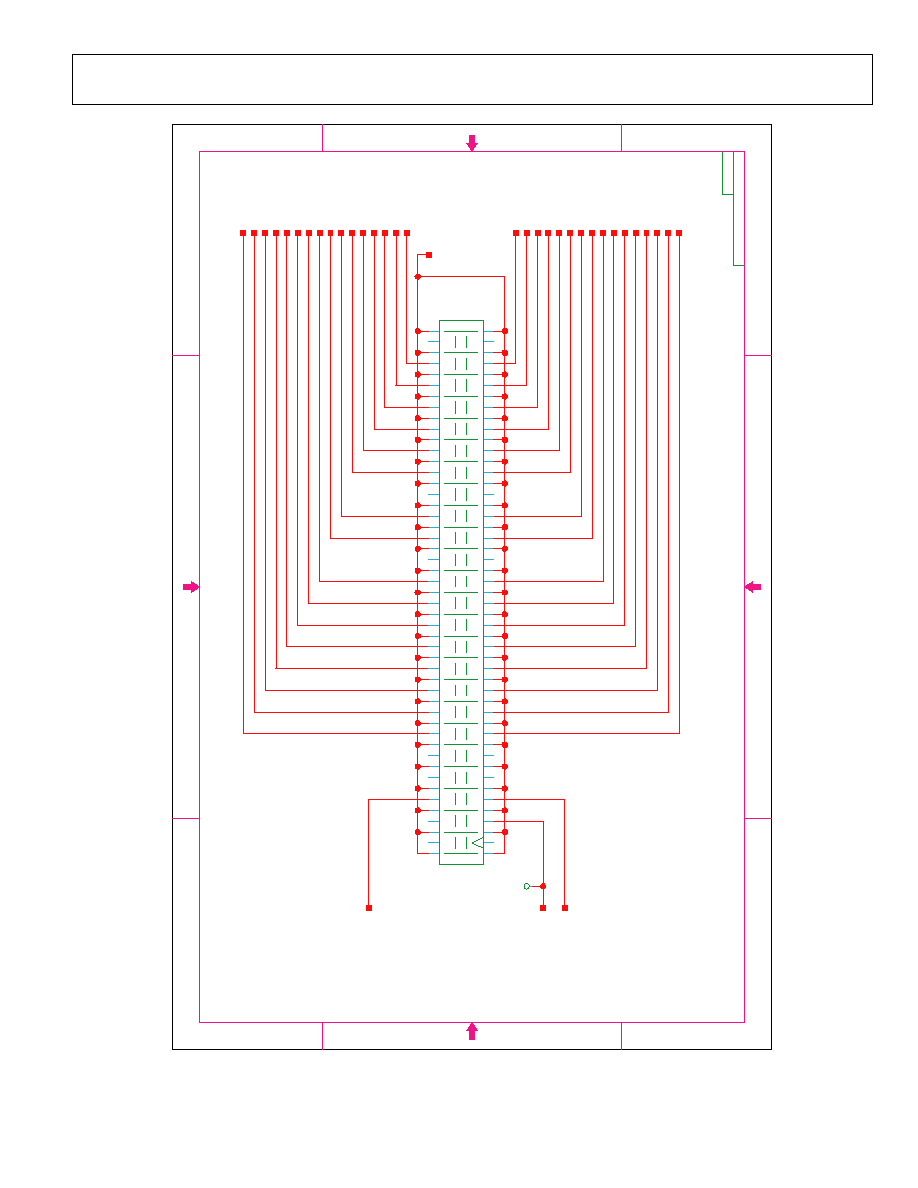
Preliminary Technical Data
AD9736/AD9735/AD9734
Rev. PrJ | Page 33 of 42
FCN-
268F
024-G
/0
D
Jack
Jack
V
E
R
1
D
C
B
A
1
2
3
4
A
B
C
D
2
3
4
F
O
5
3
N
E
G
O
R
D
Y
H
C
N
3
1
B
D
N
2
1
B
D
P
3
1
B
D
P
2
1
B
D
P
T
U
O
T
S
E
T
N
T
U
O
T
S
E
T
5
1
P
T
T
H
W
S
S
V
P
1
1
B
D
K
L
C
T
X
E
P
0
1
B
D
P
8
B
D
P
7
B
D
N
7
B
D
N
6
B
D
N
0
B
D
N
1
B
D
N
2
B
D
N
3
B
D
N
4
B
D
N
5
B
D
P
0
B
D
P
1
B
D
P
2
B
D
P
3
B
D
P
4
B
D
P
5
B
D
G2
1
S
S2
G3
G4
S3
S4
G5
G6
S5
S6
G7
G8
S7
S8
G9
G1
0
S9
S10
G11
G1
2
S11
S1
2
G13
G1
4
S13
S1
4
G15
G1
6
S15
S1
6
G17
G1
8
S17
S1
8
G19
G2
0
S19
S2
0
G21
G2
2
S21
S2
2
G23
G2
4
S23
S2
4
G25
G2
6
S25
S2
6
G27
G2
8
S27
S2
8
G29
G3
0
S29
S3
0
G31
G3
2
S31
S3
2
G33
G3
4
S33
S3
4
G35
G3
6
S35
S3
6
G37
G3
8
S37
S3
8
G39
G4
0
S39
S4
0
G41
G4
2
S41
S4
2
G43
G4
4
S43
S4
4
G45
G4
6
S45
S4
6
G47
G4
8
S47
S4
8
G49
G5
0
G1
3
J
N
I
N
K
L
C
D
T
U
O
N
K
L
C
D
N
8
B
D
N
9
B
D
N
0
1
B
D
N
1
1
B
D
P
6
B
D
N
I
P
K
L
C
D
T
U
O
P
K
L
C
D
P
9
B
D
Figure 39. High Speed Digital I/O Connector, AD9736 Evaluation Board, Rev C
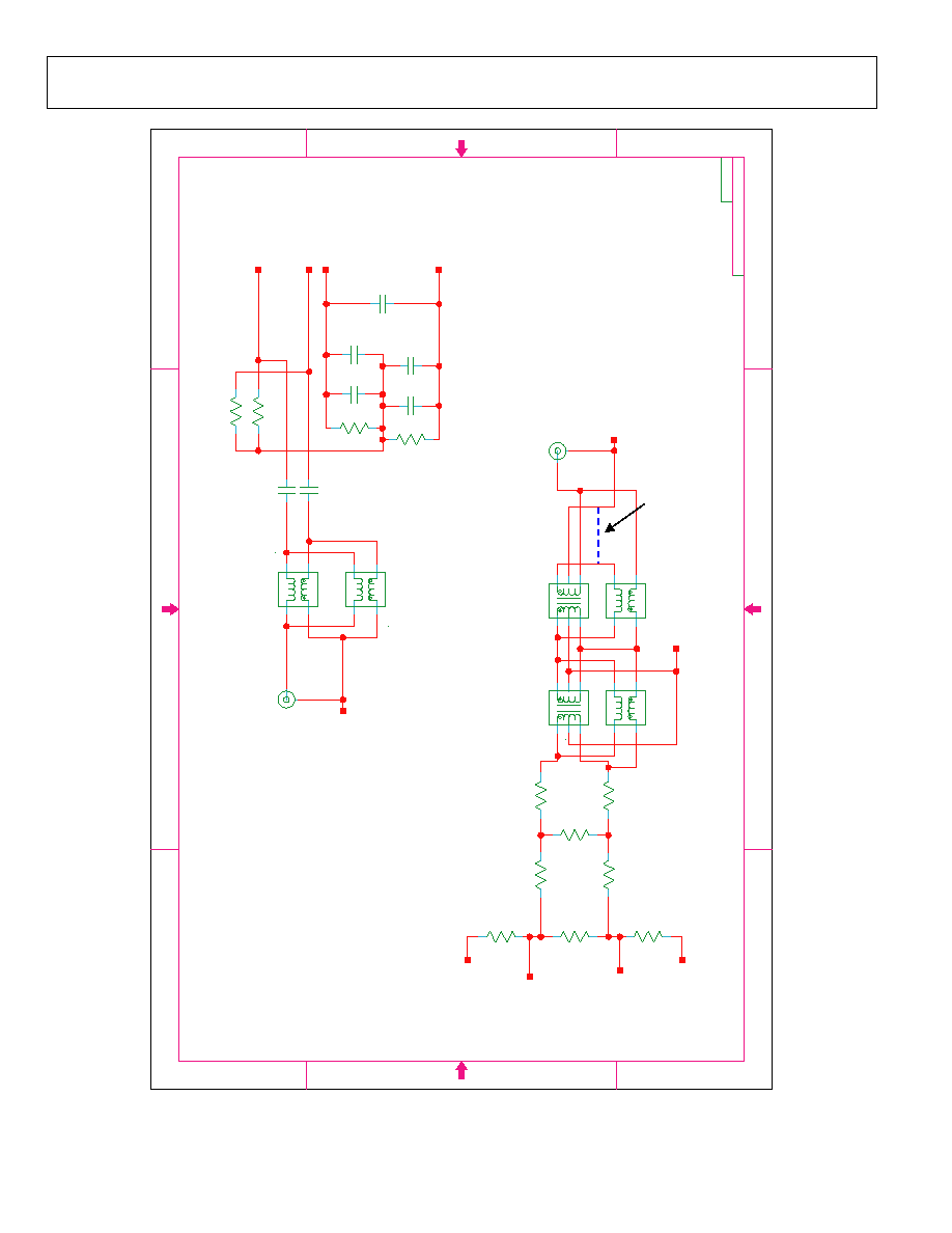
AD9736/AD9735/AD9734
Preliminary Technical Data
Rev. PrJ | Page 34 of 42
3
1
-
1
-
1
C
T
E
2
=
C
N
P
S
CC
0603
3
0
6
0
C
C
3
0
6
0
C
R
3
0
6
0
C
R
3
1
-
1
-
1
C
T
E
2
=
C
N
S
P
3
0
6
0
C
R
RC06
03
RC
0603
3
0
6
0
C
C
3
0
6
0
C
C
RC
0603
X
X
2
1
-
1
L
T
D
A
S
P
RC06
03
RC
0603
RC
0603
3
0
6
0
C
C
3
0
6
0
C
R
3
0
6
0
C
R
3
0
6
0
C
R
V
E
R
1
D
C
B
A
1
2
3
4
A
B
C
D
2
3
4
F
O
3
0
6
0
C
C
CC
0603
P
1
-
T
1
-
2
T
D
A
S
P
P
1
-
T
1
-
2
T
D
A
S
P
3
1
-
1
-
1
C
T
E
2
=
C
N
P
S
A
S
S
V
3
5
1
4
B
4
T
A
S
S
V
1
2
3
4
5
6
1
T
6
5
3
4
2
1
2
T
P
K
L
C
N
K
L
C
5
3
C
F
U
1
.
0
8
2
C
F
U
1
.
0
A
S
S
V
5
4
N
E
G
O
R
D
Y
H
C
2
6
1
R
P
N
D
1
6
1
R
P
N
D
7
1
R
P
N
D
7
2
C
P
N
D
N
I
P
I
8
R
P
N
D
6
R
P
N
D
7
R
9
.
9
4
1
4
3
6
A
3
T
3
R
K
1
P
U
0
0
2
A
M
S
1
J
5
,
4
,
3
;
A
S
S
V
P
U
0
0
2
A
M
S
5
,
4
,
3
;
A
S
S
V
2
J
9
2
C
F
N
1
6
2
C
P
N
D
4
R
0
0
3
8
1
R
P
N
D
9
1
R
P
N
D
A
S
S
V
A
S
S
V
3
1
5
4
B
3
T
5
2
0
2
R
5
2
1
2
R
F
N
1
8
3
C
C
D
D
V
A
S
S
V
F
U
1
.
0
6
3
C
4
5
1
3
3
T
Figure 40. Clock Input and Analog Output, AD9736 Evaluation Board, Rev C
NOTE:
T1, T3 & T3B are installed,
R6 & R8 = 50 ohms,
R17 & R19 = 20 ohms,
R161 & R162 = 0 ohms,
R7 = Open
Jumper added from T1 pin 3
to T1 pin 2
Jumper Added

Preliminary Technical Data
AD9736/AD9735/AD9734
Rev. PrJ | Page 35 of 42
B
A
B
A
2
4
1
C
A
4
7
4
1
C
A
4
7
4
1
C
A
4
7
4
1
C
A
4
7
4
1
C
A
4
7
4
1
C
A
4
7
4
1
C
A
4
7
4
1
C
A
4
7
4
1
C
A
4
7
4
1
C
A
4
7
5
0
8
0
C
R
5
0
8
0
C
R
5
0
8
0
C
R
RC
0603
RC
0603
0
1
2
1
C
L
0
1
2
1
C
L
E
S
A
C
A
5
0
8
0
C
C
E
S
A
C
A
5
0
8
0
C
C
4
1
C
A
4
7
2
B
A
4
1
C
A
4
7
B
A
B
A
B
A
V
E
R
1
D
C
B
A
1
2
3
4
A
B
C
D
2
3
4
F
O
T
R
O
P
I
P
S
5
5
N
E
G
O
R
D
Y
H
C
A
_
T
E
S
E
R
3
1
2
3
1
P
J
5
P
J
B
S
C
P
S
2
3
1
4
1
P
J
K
L
C
P
S
6
P
J
I
D
S
P
S
2
3
1
9
P
J
7
P
J
0
1
1
1
4
1
;
3
3
D
D
V
7
;
S
S
V
6
U
O
D
S
P
S
3
1
2
0
1
P
J
2
P
J
Q
R
I
8
9
6
U
7
;
S
S
V
4
1
;
3
3
D
D
V
3
3
C
F
U
1
.
2
3
C
F
U
7
.
4
V
3
.
6
1
3
C
F
U
1
.
0
3
C
F
U
7
.
4
V
3
.
6
E
T
I
R
R
E
F
9
L
6
1
2
4
5
3
1
P
S
S
V
S
S
V
E
T
I
R
R
E
F
8
L
K
0
1
4
1
R
3
1
R
K
0
1
K
9
2
1
R
K
9
1
1
R
K
9
0
1
R
3
4
4
1
;
3
3
D
D
V
7
;
S
S
V
5
U
1
2
5
U
7
;
S
S
V
4
1
;
3
3
D
D
V
2
1
4
1
;
3
3
D
D
V
7
;
S
S
V
6
U
3
3
D
D
V
2
1
3
1
6
U
7
;
S
S
V
4
1
;
3
3
D
D
V
1
1
0
1
4
1
;
3
3
D
D
V
7
;
S
S
V
5
U
3
1
2
1
5
U
7
;
S
S
V
4
1
;
3
3
D
D
V
5
6
5
U
7
;
S
S
V
4
1
;
3
3
D
D
V
6
5
6
U
7
;
S
S
V
4
1
;
3
3
D
D
V
4
3
4
1
;
3
3
D
D
V
7
;
S
S
V
6
U
9
8
4
1
;
3
3
D
D
V
7
;
S
S
V
5
U
S
S
V
3
3
D
D
V
S
S
V
3
3
D
D
V
S
S
V
3
3
D
D
V
S
S
V
3
3
D
D
V
S
S
V
3
3
D
D
V
2
3
1
1
1
P
J
S
S
V
3
3
D
D
V
3
1
2
2
1
P
J
Figure 41. SPI Port Interface, AD9736 Evaluation Board, Rev C

AD9736/AD9735/AD9734
Preliminary Technical Data
Rev. PrJ | Page 36 of 42
AD9736 EVALUATION BOARD PCB LAYOUT
Figure 42. PCB Layout Top Placement, AD9736 Evaluation Board, Rev C
NOTE:
AD9736 is soldered
directly to the PCB,
the socket is not
installed.
Silkscreen Error:
SPI
PIN
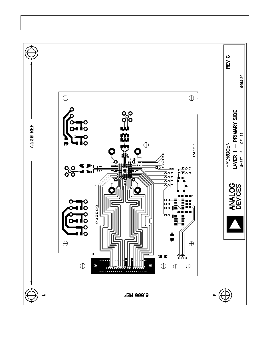
Preliminary Technical Data
AD9736/AD9735/AD9734
Rev. PrJ | Page 37 of 42
Figure 43. PCB Layout Layer 1, AD9736 Evaluation Board, Rev C
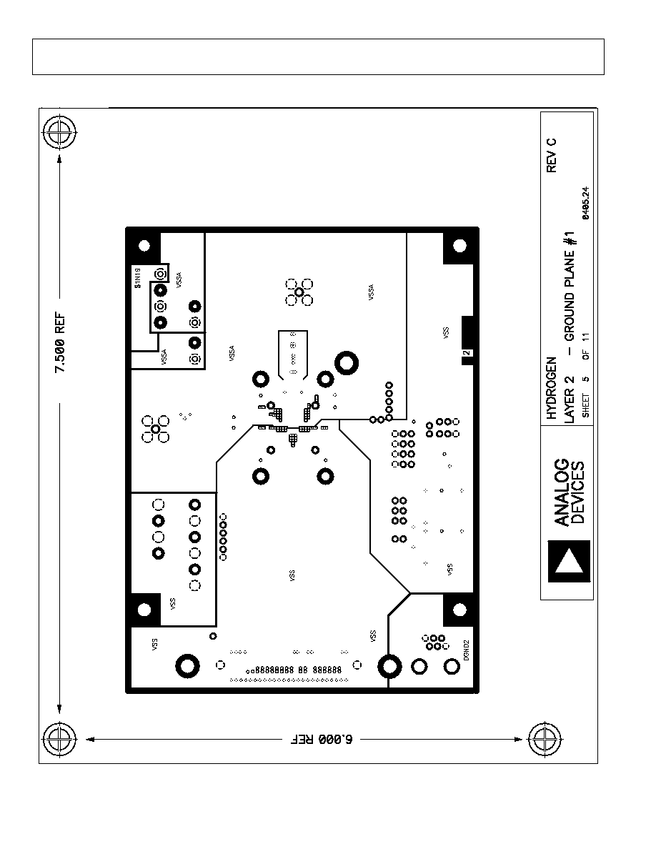
AD9736/AD9735/AD9734
Preliminary Technical Data
Rev. PrJ | Page 38 of 42
Figure 44. PCB Layout Layer 2, AD9736 Evaluation Board, Rev C
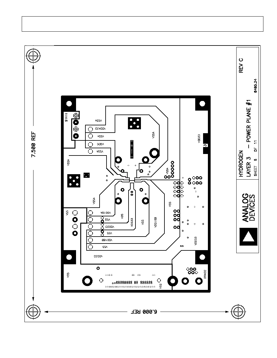
Preliminary Technical Data
AD9736/AD9735/AD9734
Rev. PrJ | Page 39 of 42
Figure 45. PCB Layout Layer 3, AD9736 Evaluation Board, Rev C
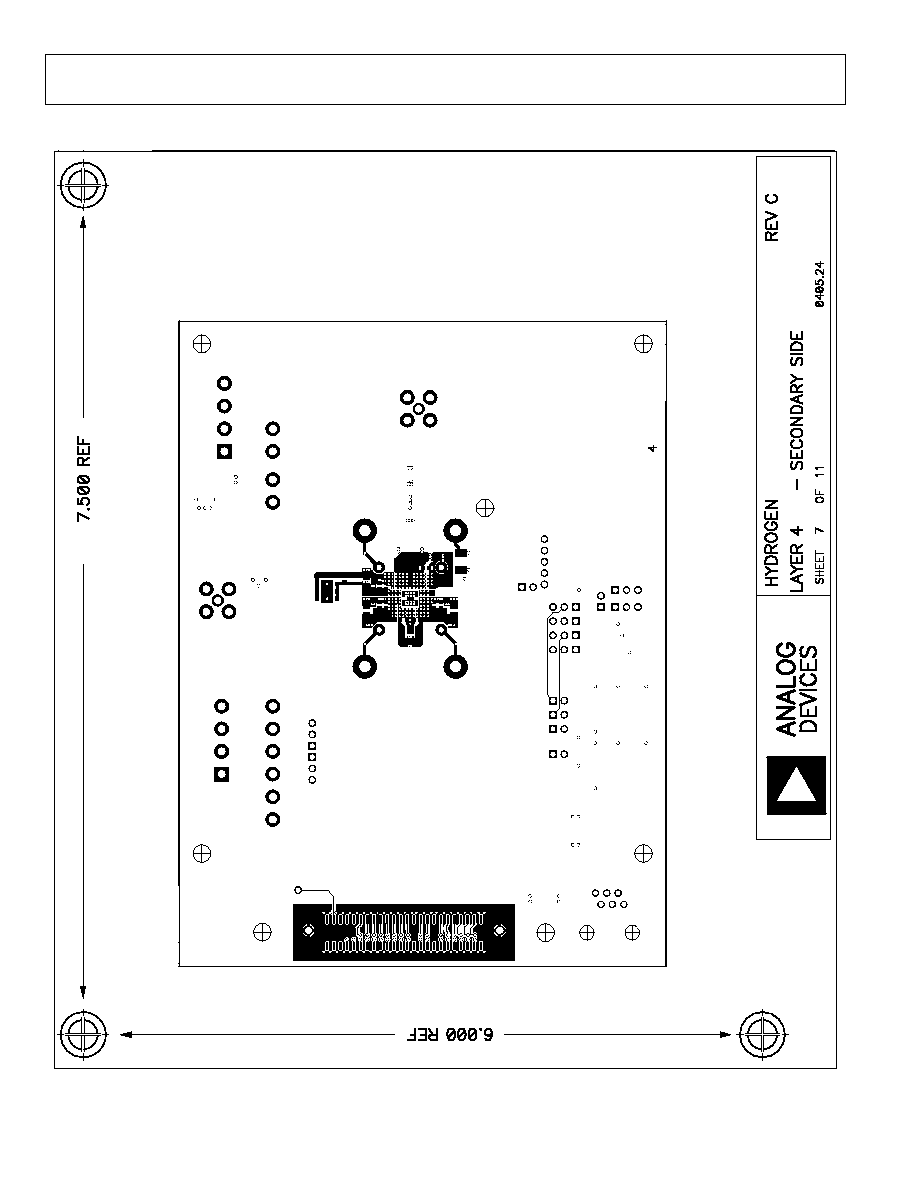
AD9736/AD9735/AD9734
Preliminary Technical Data
Rev. PrJ | Page 40 of 42
Figure 46. PCB Layout Layer 4, AD9736 Evaluation Board, Rev C
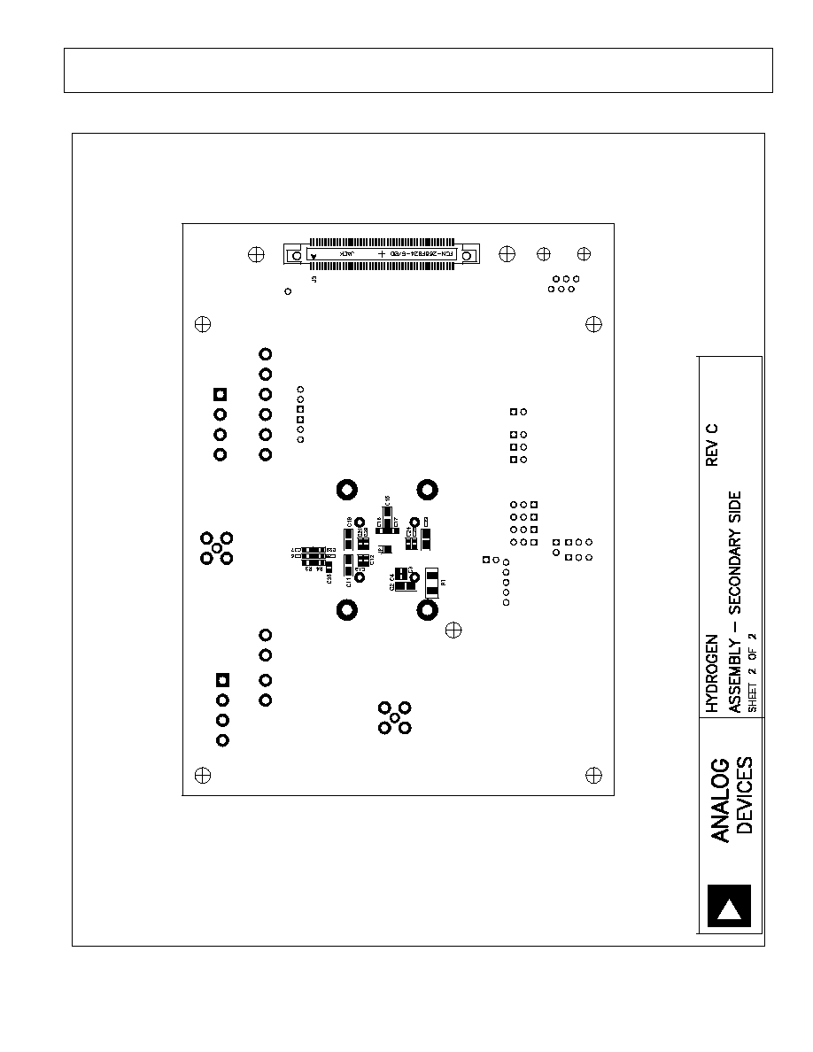
Preliminary Technical Data
AD9736/AD9735/AD9734
Rev. PrJ | Page 41 of 42
Figure 47. PCB Layout Bottom Placement, AD9736 Evaluation Board, Rev C
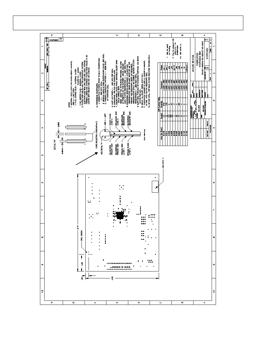
AD9736/AD9735/AD9734
Preliminary Technical Data
Rev. PrJ | Page 42 of 42
Figure 48. PCB Fabrication Detail, AD9736 Evaluation Board, Rev C
NOTE:
Special layer stack
to control LVDS
trace impedance.
PR04862-0-9/04(PrJ)