 | –≠–ª–µ–∫—Ç—Ä–æ–Ω–Ω—ã–π –∫–æ–º–ø–æ–Ω–µ–Ω—Ç: AD974 | –°–∫–∞—á–∞—Ç—å:  PDF PDF  ZIP ZIP |
REV. A
Information furnished by Analog Devices is believed to be accurate and
reliable. However, no responsibility is assumed by Analog Devices for its
use, nor for any infringements of patents or other rights of third parties
which may result from its use. No license is granted by implication or
otherwise under any patent or patent rights of Analog Devices.
a
AD974
One Technology Way, P.O. Box 9106, Norwood, MA 02062-9106, U.S.A.
Tel: 781/329-4700
World Wide Web Site: http://www.analog.com
Fax: 781/326-8703
© Analog Devices, Inc., 1999
4-Channel, 16-Bit, 200 kSPS
Data Acquisition System
FUNCTIONAL BLOCK DIAGRAM
CONTROL LOGIC
&
CALIBRATION CIRCUITRY
PWRD
V1A
V1B
BIP
CAP
REF
V
DIG
V
ANA
EXT/
INT
DATACLK
R/
C
CS
SYNC
DGND
BUSY
WR2
WR1
A1
A0
AGND2
AGND1
REF
BUFF
2.5V
REFERENCE
AD974
4 TO 1
MUX
+
LATCH
EN
V2A
V2B
V3A
V3B
V4A
V4B
SWITCHED
CAP ADC
SERIAL
INTERFACE
16
DATA
RESISTIVE
NETWORK
RESISTIVE
NETWORK
RESISTIVE
NETWORK
RESISTIVE
NETWORK
CLOCK
FEATURES
Fast 16-Bit ADC with 200 kSPS Throughput
Four Single-Ended Analog Input Channels
Single +5 V Supply Operation
Input Ranges: 0 V to +4 V, 0 V to +5 V and 10 V
120 mW Max Power Dissipation
Power-Down Mode 50 W
Choice of External or Internal 2.5 V Reference
On-Chip Clock
Power-Down Mode
GENERAL DESCRIPTION
The AD974 is a four-channel, data acquisition system with a
serial interface. The part contains an input multiplexer, a high-
speed 16-bit sampling ADC and a +2.5 V reference. All of this
operates from a single +5 V power supply that also has a power-
down mode. The part will accommodate 0 V to +4 V, 0 V to
+5 V or
±
10 V analog input ranges.
The interface is designed for an efficient transfer of data while
requiring a low number of interconnects.
The AD974 is comprehensively tested for ac parameters such as
SNR and THD, as well as the more traditional parameters of
offset, gain and linearity.
The AD974 is fabricated on Analog Devices' BiCMOS process,
which has high performance bipolar devices along with CMOS
transistors.
The AD974 is available in 28-lead DIP, SOIC and SSOP
packages.
PRODUCT HIGHLIGHTS
1. The AD974 is a complete data acquisition system combining
a four-channel multiplexer, a 16-bit sampling ADC and a
+2.5 V reference on a single chip.
2. The part operates from a single +5 V supply and also has a
power-down feature.
3. Interfacing to the AD974 is simple with a low number of
interconnect signals.
4. The AD974 is comprehensively specified for ac parameters
such as SNR and THD, as well as dc parameters such as
linearity and offset and gain errors.

REV. A
≠2≠
AD974≠SPECIFICATIONS
A Grade
B Grade
Parameter
Conditions
Min
Typ
Max
Min
Typ
Max
Units
RESOLUTION
16
16
Bits
ANALOG INPUT
Voltage Range
±
10 V, 0 V to +4 V, 0 V to +5 V (See Table I)
Impedance
Channel On or Off
(See Table I)
Sampling Capacitance
40
40
pF
THROUGHPUT SPEED
Complete Cycle
(Acquire and Convert)
5
5
µ
s
Throughput Rate
200
200
kHz
DC ACCURACY
Integral Linearity Error
±
3
±
2.0
LSB
1
Differential Linearity Error
≠2
+3
≠1
+1.75
LSB
No Missing Codes
15
16
Bits
Transition Noise
2
1.0
1.0
LSB
Full-Scale Error
3
Internal Reference
±
0.5
±
0.25
%
Full-Scale Error Drift
Internal Reference
±
7
±
7
ppm/
∞
C
Full-Scale Error
Ext. REF = +2.5 V
±
0.5
±
0.25
%
Full-Scale Error Drift
Ext. REF = +2.5 V
±
2
±
2
ppm/
∞
C
Bipolar Zero Error
Bipolar Range
±
10
±
10
mV
Bipolar Zero Error Drift
Bipolar Range
±
2
±
2
ppm/
∞
C
Unipolar Zero Error
Unipolar Ranges
±
10
±
10
mV
Unipolar Zero Error Drift
Unipolar Ranges
±
2
±
2
ppm/
∞
C
Channel-to-Channel Matching
±
0.1
±
0.05
% FSR
Recovery to Rated Accuracy
After Power-Down
4
2.2
µ
F to CAP
1
1
ms
Power Supply Sensitivity
V
ANA
= V
DIG
= V
D
V
D
= 5 V
±
5%
±
8
±
8
LSB
AC ACCURACY
Spurious Free Dynamic Range
f
IN
= 20 kHz
90
96
dB
5
Total Harmonic Distortion
f
IN
= 20 kHz
≠90
≠96
dB
Signal-to-(Noise+Distortion)
f
IN
= 20 kHz
83
85
dB
≠60 dB Input
27
28
dB
Signal-to-Noise
f
IN
= 20 kHz
83
85
dB
Channel-to-Channel Isolation
f
IN
= 20 kHz
≠110
≠100
≠110
≠100
dB
Full Power Bandwidth
6
1
1
MHz
≠3 dB Input Bandwidth
2.7
2.7
MHz
SAMPLING DYNAMICS
Aperture Delay
40
40
ns
Transient Response
Full-Scale Step
1
1
µ
s
Overvoltage Recovery
7
150
150
ns
REFERENCE
Internal Reference Voltage
2.48
2.5
2.52
2.48
2.5
2.52
V
Internal Reference Source Current
1
1
µ
A
External Reference Voltage Range
for Specified Linearity
2.3
2.5
2.7
2.3
2.5
2.7
V
External Reference Current Drain
Ext. REF = +2.5 V
100
100
µ
A
DIGITAL INPUTS
Logic Levels
V
IL
≠0.3
+0.8
≠0.3
+0.8
V
V
IH
+2.0
V
DIG
+ 0.3
+2.0
V
DIG
+ 0.3
V
I
IL
±
10
±
10
µ
A
I
IH
±
10
±
10
µ
A
(≠40 C to +85 C, f
S
= 200 kHz, V
DIG
= V
ANA
= +5 V, unless otherwise noted)
REV. A
≠3≠
AD974
A Grade
B Grade
Parameter
Conditions
Min
Typ
Max
Min
Typ
Max
Units
DIGITAL OUTPUTS
Data Format
Serial 16 Bits
Data Coding
Straight Binary
V
OL
I
SINK
= 1.6 mA
+0.4
+0.4
V
V
OH
I
SOURCE
= 500
µ
A
+4
+4
V
Output Capacitance
High-Z State
15
15
pF
Leakage Current
High-Z State
V
OUT
= 0 V to V
DIG
±
5
±
5
µ
A
POWER SUPPLIES
Specified Performance
V
DIG
+4.75
+5
+5.25
+4.75 +5
+5.25
V
V
ANA
+4.75
+5
+5.25
+4.75 +5
+5.25
V
I
DIG
4.5
4.5
mA
I
ANA
14
14
mA
Power Dissipation
PWRD LOW
120
120
mW
PWRD HIGH
50
50
µ
W
TEMPERATURE RANGE
Specified Performance
T
MIN
to T
MAX
≠40
+85
≠40
+85
∞
C
NOTES
1
LSB means Least Significant Bit. With a
±
10 V input, one LSB is 305
µ
V.
2
Typical rms noise at worst case transitions and temperatures.
3
Full-Scale Error is expressed as the % difference between the actual full-scale code transition voltage and the ideal full-scale transition voltage, and includes the effect
of offset error. For bipolar input, the Full-Scale Error is the worst case of either the ≠Full-Scale or +Full-Scale code transition voltage errors. For unipolar input
ranges, Full-Scale Error is with respect to the +Full-Scale code transition voltage.
4
External 2.5 V reference connected to REF.
5
All specifications in dB are referred to a full-scale
±
10 V input.
6
Full-Power Bandwidth is defined as full-scale input frequency at which Signal-to-(Noise + Distortion) degrades to 60 dB, or 10 bits of accuracy.
7
Recovers to specified performance after a 2
◊
FS input overvoltage.
Specifications subject to change without notice.
TIMING SPECIFICATIONS
Parameter
Symbol
Min
Typ
Max
Units
Convert Pulsewidth
t
1
50
ns
R/
C, CS to BUSY Delay
t
2
100
ns
BUSY LOW Time
t
3
4.0
µ
s
BUSY Delay after End of Conversion
t
4
50
ns
Aperture Delay
t
5
40
ns
Conversion Time
t
6
3.8
4.0
µ
s
Acquisition Time
t
7
1.0
µ
s
Throughput Time
t
6
+ t
7
5
µ
s
R/
C Low to DATACLK Delay
t
8
220
ns
DATACLK Period
t
9
220
ns
DATA Valid Setup Time
t
10
50
ns
DATA Valid Hold Time
t
11
20
ns
EXT. DATACLK Period
t
12
66
ns
EXT. DATACLK HIGH
t
13
20
ns
EXT. DATACLK LOW
t
14
30
ns
R/
C, CS to EXT. DATACLK Setup Time
t
15
20
t
12
+ 5
ns
R/
C to CS Setup Time
t
16
10
ns
EXT. DATACLK to SYNC Delay
t
17
15
66
ns
EXT. DATACLK to DATA Valid Delay
t
18
25
66
ns
CS to EXT. DATACLK Rising Edge Delay
t
19
10
ns
Previous DATA Valid after
CS, R/C Low
t
20
3.5
µ
s
BUSY to EXT. DATACLK Setup Time
t
21
5
ns
Final EXT. DATACLK to
BUSY Rising Edge
t
22
1.7
µ
s
A0, A1 to
WR1, WR2 Setup Time
t
23
10
ns
A0, A1 to
WR1, WR2 Hold Time
t
24
10
ns
WR1, WR2 Pulsewidth
t
25
50
ns
Specifications subject to change without notic e.
(f
S
= 200 kHz, V
DIG
= V
ANA
= +5 V, ≠40 C to +85 C)
REV. A
AD974
≠4≠
CAUTION
ESD (electrostatic discharge) sensitive device. Electrostatic charges as high as 4000 V readily
accumulate on the human body and test equipment and can discharge without detection.
Although the AD974 features proprietary ESD protection circuitry, permanent damage may
occur on devices subjected to high energy electrostatic discharges. Therefore, proper ESD
precautions are recommended to avoid performance degradation or loss of functionality.
WARNING!
ESD SENSITIVE DEVICE
ABSOLUTE MAXIMUM RATINGS
1
Analog Inputs
VxA, VxB . . . . . . . . . . . . . . . . . . . . . . . . . . . . . . . . . .
±
25 V
CAP . . . . . . . . . . . . . . . . +V
ANA
+ 0.3 V to AGND2 ≠ 0.3 V
REF . . . . . . . . . . . . . . . . . . . . Indefinite Short to AGND2,
Momentary Short to V
ANA
Ground Voltage Differences
DGND, AGND1, AGND2 . . . . . . . . . . . . . . . . . . .
±
0.3 V
Supply Voltages
V
ANA
. . . . . . . . . . . . . . . . . . . . . . . . . . . . . . . . . . . . . . +7 V
V
DIG
to V
ANA
. . . . . . . . . . . . . . . . . . . . . . . . . . . . . . . .
±
7 V
V
DIG
. . . . . . . . . . . . . . . . . . . . . . . . . . . . . . . . . . . . . . +7 V
Digital Inputs . . . . . . . . . . . . . . . . . . . ≠0.3 V to V
DIG
+ 0.3 V
Internal Power Dissipation
2
PDIP (N), SOIC (R), SSOP (RS) . . . . . . . . . . . . . 700 mW
Junction Temperature . . . . . . . . . . . . . . . . . . . . . . . . . +150
∞
C
Storage Temperature Range N, R . . . . . . . . ≠65
∞
C to +150
∞
C
Lead Temperature Range
(Soldering 10 sec) . . . . . . . . . . . . . . . . . . . . . . . . . . +300
∞
C
NOTES
1
Stresses above those listed under Absolute Maximum Ratings may cause perma-
nent damage to the device. This is a stress rating only; functional operation of the
device at these or any other conditions above those indicated in the operational
section of this specification is not implied. Exposure to absolute maximum rating
conditions for extended periods may affect device reliability.
2
Specification is for device in free air:
28-Lead PDIP:
JA
= 100
∞
C/W,
JC
= 31
∞
C/W
28-Lead SOIC:
JA
= 75
∞
C/W,
JC
= 24
∞
C/W
28-Lead SSOP:
JA
= 109
∞
C/W,
JC
= 39
∞
C/W
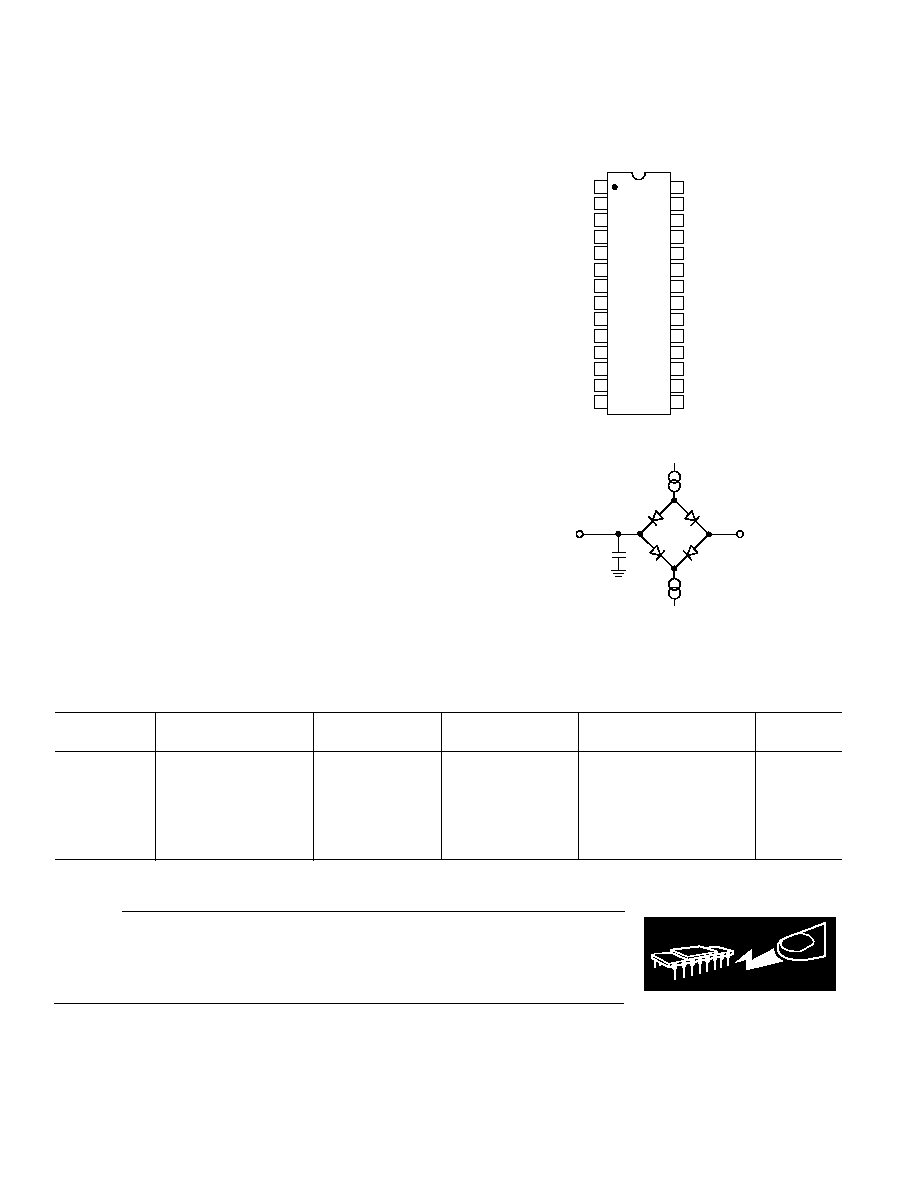
PIN CONFIGURATION
SOIC, DIP AND SSOP
TOP VIEW
(Not to Scale)
28
27
26
25
24
23
22
21
20
19
18
17
16
15
1
2
3
4
5
6
7
8
9
10
11
12
13
14
AD974
DGND
EXT/
INT
PWRD
V
DIG
R/
C
AGND2
REF
AGND1
V3A
V3B
V4A
CAP
BIP
V4B
SYNC
DATACLK
DATA
WR2
WR1
CS
BUSY
V2B
V2A
V1B
V1A
A1
A0
V
ANA
TO OUTPUT
PIN
C
L
100pF
I
OL
+1.4V
I
OH
1.6mA
500 A
Figure 1. Load Circuit for Digital Interface Timing
ORDERING GUIDE
Temperature
Package
Package
Model
Range
Max INL
Min S/(N+D)
Description
Options
AD974AN
≠40
∞
C to +85
∞
C
±
3.0 LSB
83 dB
28-Lead Plastic DIP
N-28B
AD974BN
≠40
∞
C to +85
∞
C
±
2.0 LSB
85 dB
28-Lead Plastic DIP
N-28B
AD974AR
≠40
∞
C to +85
∞
C
±
3.0 LSB
83 dB
28-Lead SOIC
R-28
AD974BR
≠40
∞
C to +85
∞
C
±
2.0 LSB
85 dB
28-Lead SOIC
R-28
AD974ARS
≠40
∞
C to +85
∞
C
±
3.0 LSB
83 dB
28-Lead SSOP
RS-28
AD974BRS
≠40
∞
C to +85
∞
C
±
2.0 LSB
85 dB
28-Lead SSOP
RS-28
REV. A
AD974
≠5≠
PIN FUNCTION DESCRIPTIONS
Pin No.
Mnemonic
Description
1
AGND1
Analog Ground. Used as the ground reference point for the REF pin.
2≠5, 25≠28
VxA, VxB
Analog Input. Refer to Table I for input range configuration.
6
BIP
Bipolar Offset. Connect VxA inputs to provide Bipolar input range.
7
CAP
Reference Buffer Output. Connect a 2.2
µ
F tantalum capacitor between CAP and Analog
Ground.
8
REF
Reference Input/Output. The internal +2.5 V reference is available at this pin. Alternatively an
external reference can be used to override the internal reference. In either case, connect a 2.2
µ
F
tantalum capacitor between REF and Analog Ground.
9
AGND2
Analog Ground.
10
R/
C
Read/
Convert Input. Used to control the conversion and read modes. With CS LOW, a falling
edge on R/
C holds the analog input signal internally and starts a conversion; a rising edge enables
the transmission of the conversion result.
11
V
DIG
Digital Power Supply. Nominally +5 V.
12
PWRD
Power-Down Input. When set to a logic HIGH, power consumption is reduced and conversions
are inhibited. The conversion result from the previous conversion is stored in the onboard shift
register.
13
EXT/
INT
Digital select input for choosing the internal or an external data clock. With EXT/
INT tied LOW,
after initiating a conversion, 16 DATACLK pulses transmit the previous conversion result as
shown in Figure 3. With EXT/
INT set to a Logic HIGH, output data is synchronized to an
external clock signal connected to the DATACLK input. Data is output as indicated in Figure 4
through Figure 9.
14
DGND
Digital Ground.
15
SYNC
Digital output frame synchronization for use with an external data clock (EXT/
INT = Logic
HIGH). When a read sequence is initiated, a pulse one DATACLK period wide is output
synchronous to the external data clock.
16
DATACLK
Serial data clock input or output, dependent upon the logic state of the EXT/
INT pin. When
using the internal data clock (EXT/
INT = Logic LOW), a conversion start sequence will initiate
transmission of 16 DATACLK periods. Output data is synchronous to this clock and is valid on
both its rising and falling edges (Figure 3). When using an external data clock (EXT/
INT = Logic
HIGH), the
CS and R/C signals control how conversion data is accessed.
17
DATA
The serial data output is synchronized to DATACLK. Conversion results are stored in an on-
chip register. The AD974 provides the conversion result, MSB first, from its internal shift regis-
ter. When using the internal data clock (EXT/
INT = Logic LOW), DATA is valid on both the
rising and falling edges of DATACLK. Using an external data clock (EXT/
INT = Logic HIGH)
allows previous conversion data to be accessed during a conversion (Figures 5, 7 and 9) or the
conversion result can be accessed after the completion of a conversion (Figures 4, 6 and 8).
18, 19
WR1, WR2
Multiplexer Write Inputs. These inputs are internally ORed to generate the mux latch inputs.
The latch is transparent when
WR1 and WR2 are tied low.
20
CS
Chip Select Input. With R/
C LOW, a falling edge on CS will initiate a conversion. With R/C
HIGH, a falling edge on
CS will enable the serial data output sequence.
21
BUSY
Busy Output. Goes LOW when a conversion is started, and remains LOW until the conversion is
completed and the data is latched into the on-chip shift register.
22, 23
A1, A0
Address multiplexer inputs latched with the
WR1, WR2 inputs.
A1
A0
Data Available from Channel
0
0
AIN 1
0
1
AIN 2
1
0
AIN 3
1
1
AIN 4
24
V
ANA
Analog Power Supply. Nominally +5 V.

REV. A
AD974
≠6≠
DEFINITION OF SPECIFICATIONS
INTEGRAL NONLINEARITY ERROR (INL)
Linearity error refers to the deviation of each individual code
from a line drawn from "negative full scale" through "positive
full scale." The point used as "negative full scale" occurs 1/2 LSB
before the first code transition. "Positive full scale" is defined as
a level 1 1/2 LSB beyond the last code transition. The deviation
is measured from the middle of each particular code to the true
straight line.
DIFFERENTIAL NONLINEARITY ERROR (DNL)
In an ideal ADC, code transitions are 1 LSB apart. Differential
nonlinearity is the maximum deviation from this ideal value. It
is often specified in terms of resolution for which no missing
codes are guaranteed.
FULL-SCALE ERROR
The last + transition (from 011 . . . 10 to 011 . . . 11) should
occur for an analog voltage 1 1/2 LSB below the nominal full
scale (9.9995422 V for a
±
10 V range). The full-scale error is
the deviation of the actual level of the last transition from the
ideal level.
BIPOLAR ZERO ERROR
Bipolar zero error is the difference between the ideal midscale
input voltage (0 V) and the actual voltage producing the mid-
scale output code.
UNIPOLAR ZERO ERROR
In unipolar mode, the first transition should occur at a level
1/2 LSB above analog ground. Unipolar zero error is the devia-
tion of the actual transition from that point.
SPURIOUS FREE DYNAMIC RANGE
The difference, in decibels (dB), between the rms amplitude of
the input signal and the peak spurious signal.
TOTAL HARMONIC DISTORTION (THD)
THD is the ratio of the rms sum of the first six harmonic com-
ponents to the rms value of a full-scale input signal and is ex-
pressed in decibels.
SIGNAL TO (NOISE AND DISTORTION) (S/[N+D]) RATIO
S/(N+D) is the ratio of the rms value of the measured input
signal to the rms sum of all other spectral components below
the Nyquist frequency, including harmonics but excluding dc.
The value for S/(N+D) is expressed in decibels.
FULL POWER BANDWIDTH
The full power bandwidth is defined as the full-scale input fre-
quency at which the S/(N+D) degrades to 60 dB, 10 bits of
accuracy.
APERTURE DELAY
Aperture delay is a measure of the acquisition performance, and
is measured from the falling edge of the R/
C input to when the
input signal is held for a conversion.
TRANSIENT RESPONSE
The time required for the AD974 to achieve its rated accuracy
after a full-scale step function is applied to its input.
OVERVOLTAGE RECOVERY
The time required for the ADC to recover to full accuracy after
an analog input signal 150% of full-scale is reduced to 50% of
the full-scale value.
REV. A
AD974
≠7≠
CONVERSION CONTROL
The AD974 is controlled by two signals: R/
C and CS. When
R/
C is brought low, with CS low, for a minimum of 50 ns, the
input signal will be held on the internal capacitor array and a
conversion "n" will begin. Once the conversion process does
begin, the
BUSY signal will go low until the conversion is com-
plete. Internally, the signals R/
C and CS are ORed together and
there is no requirement on which signal is taken low first when
initiating a conversion. The only requirement is that there be at
least 10 ns of delay between the two signals being taken low.
After the conversion is complete, the
BUSY signal will return
high and the AD974 will again resume tracking the input signal.
Under certain conditions the
CS pin can be tied Low and R/C
will be used to determine whether you are initiating a conver-
sion or reading data. On the first conversion, after the AD974 is
powered up, the DATA output will be indeterminate.
Conversion results can be clocked serially, using either an
internal clock generated by the AD974 or an external clock.
The AD974 is configured for the internal data clock mode by
pulling the EXT/
INT pin low. It is configured for the external
clock mode by pulling the EXT/
INT pin high.
INTERNAL DATA CLOCK MODE
The AD974 is configured to generate and provide the data clock
when the EXT/
INT pin is held low. Typically CS will be tied
low and R/
C will be used to initiate a conversion "n." During
the conversion the AD974 will output 16 bits of data, MSB first,
from conversion "n-1" on the DATA pin. This data will be
synchronized with 16 clock pulses provided on the DATACLK
pin. The output data will be valid on both the rising and falling
edge of the data clock as shown in Figure 3. After the LSB has
been presented, the DATACLK pin will stay low until another
conversion is initiated.
In this mode, the digital input/output pins' transitions are suit-
ably positioned to minimize degradation on the conversion
result, mainly during the second half of the conversion process.
EXTERNAL DATA CLOCK MODE
The AD974 is configured to accept an externally supplied data
clock when the EXT/
INT pin is held high. This mode of opera-
tion provides several methods by which conversion results can
be read. The output data from conversion "n-1" can be read
during conversion "n," or the output data from conversion "n"
CS
, R/
C
BUSY
MODE
ACQUIRE
CONVERT
t
1
CONVERT
ACQUIRE
t
3
t
2
t
5
t
6
t
4
t
7
t
23
t
25
t
24
A0, A1
WR1
,
WR2
Figure 2. Basic Conversion Timing
R/
C
DATACLK
DATA
BUSY
1
MSB
VALID
BIT 14
VALID
t
8
t
1
t
9
2
3
15
16
t
10
t
11
BIT 13
VALID
BIT 1
VALID
LSB
VALID
t
2
t
6
Figure 3. Serial Data Timing for Reading Previous Conversion Results with Internal Clock
(
CS and EXT/ INT Set to Logic Low)

REV. A
AD974
≠8≠
can be read after the conversion is complete. The external clock
can be either a continuous or discontinuous clock. A discontinu-
ous clock can be either normally low or normally high when
inactive. In the case of the discontinuous clock, the AD974 can be
configured to either generate or not generate a SYNC output
(with a continuous clock a SYNC output will always be produced).
Each of the methods will be described in the following sections
and are illustrated in Figures 4 through 9. It should be noted
that all timing diagrams assume that the receiving device is
latching data on the rising edge of the external clock. If the
falling edge of DATACLK is used then, in the case of a discon-
tinuous clock, one less clock pulse is required than shown in
Figures 4 through 7 to latch in a 16-bit word. Note that data is
valid on the falling edge of a clock pulse (for t
13
greater than t
18
)
and the rising edge of the next clock pulse.
The AD974 provides error correction circuitry that can correct
for an improper bit decision made during the first half of the
conversion cycle. Normally the occurrence of an incorrect bit
decision during a conversion cycle is irreversible. This error
occurs as a result of noise during the time of the decision or due
to insufficient settling time. As the AD974 is performing a
conversion it is important that transitions not occur on digital
input/output pins or degradation of the conversion result could
occur. This is particularly important during the second half of
the conversion process. For this reason it is recommended that
when an external clock is being provided it be a discontinuous
clock that is not toggling during the time that
BUSY is low or,
more importantly, that it does not transition during the latter
half of
BUSY low.
EXTERNAL DISCONTINUOUS CLOCK DATA READ
AFTER CONVERSION WITH NO SYNC OUTPUT
GENERATED
Figure 4 illustrates the method by which data from conversion
"n" can be read after the conversion is complete using a discon-
tinuous external clock without the generation of a SYNC
output. After a conversion is complete, indicated by
BUSY
returning high, the result of that conversion can be read while
CS is Low and R/C is high. In this mode CS can be tied low.
The MSB will be valid on the first falling edge and the second
rising edge of DATACLK. The LSB will be valid on the 16th
falling edge and the 17th rising edge of DATACLK. A mini-
mum of 16 clock pulses are required for DATACLK if the
receiving device will be latching data on the falling edge of
DATACLK. A minimum of 17 clock pulses are required for
DATACLK if the receiving device will be latching data on the
rising edge of DATACLK.
The advantage of this method of reading data is that data is not
being clocked out during a conversion and therefore conversion
performance is not degraded.
When reading data after the conversion is complete, with the
highest frequency permitted for DATACLK (15.15 MHz), the
maximum possible throughput is approximately 195 kHz, and
not the rated 200 kHz.
EXT
DATACLK
R/
C
BUSY
SYNC
DATA
t
12
0
1
2
3
14
15
16
t
13
t
14
t
1
t
2
t
21
t
18
t
18
BIT 15
(MSB)
BIT 14
BIT 13
BIT 1
BIT 0
(LSB)
Figure 4. Conversion and Read Timing Using an External Discontinuous Data Clock
(EXT/
INT Set to Logic High, CS Set to Logic Low)

REV. A
AD974
≠9≠
EXTERNAL DISCONTINUOUS CLOCK DATA READ
DURING CONVERSION WITH NO SYNC OUTPUT
GENERATED
Figure 5 illustrates the method by which data from conversion
"n-1" can be read during conversion "n" while using a discon-
tinuous external clock, without the generation of a SYNC out-
put. After a conversion is initiated, indicated by
BUSY going
low, the result of the previous conversion can be read while
CS
is low and R/
C is high. In this mode CS can be tied low. The
MSB will be valid on the 1st falling edge and the 2nd rising edge of
DATACLK. The LSB will be valid on the 16th falling edge and
the 17th rising edge of DATACLK. A minimum of 16 clock
pulses are required for DATACLK if the receiving device will be
latching data on the falling edge of DATACLK. A minimum of
17 clock pulses are required for DATACLK if the receiving
device will be latching data on the rising edge of DATACLK.
In this mode the data should be clocked out during the first half
of
BUSY so not to degrade conversion performance. This re-
quires use of a 10 MHz DATACLK or greater, with data being
read out as soon as the conversion process begins.
EXTERNAL DISCONTINUOUS CLOCK DATA READ
AFTER CONVERSION WITH SYNC OUTPUT GENERATED
Figure 6 illustrates the method by which data from conver-
sion "n" can be read after the conversion is complete using a
discontinuous external clock, with the generation of a SYNC
output. What permits the generation of a SYNC output is a
transition of DATACLK while either
CS is high or while both
CS and R/C are low. After a conversion is complete, indicated
by
BUSY returning high, the result of that conversion can be
read while
CS is Low and R/C is high. In this mode CS can be
tied low. In Figure 6 clock pulse #0 is used to enable the gen-
eration of a SYNC pulse. The SYNC pulse is actually clocked
out approximately 40 ns after the rising edge of clock pulse #1.
The SYNC pulse will be valid on the falling edge of clock pulse
#1 and the rising edge of clock pulse #2. The MSB will be valid
on the falling edge of clock pulse #2 and the rising edge of clock
pulse #3. The LSB will be valid on the falling edge of clock
pulse #17 and the rising edge of clock pulse #18. The advan-
tage of this method of reading data is that it is not being clocked
out during a conversion and therefore conversion performance is
not degraded.
When reading data after the conversion is complete, with the
highest frequency permitted for DATACLK (15.15 MHz), the
maximum possible throughput is approximately 195 kHz and
not the rated 200 kHz.
EXT
DATACLK
R/
C
BUSY
SYNC
DATA
0
BIT 15
(MSB)
BIT 14
t
12
t
13
t
14
1
2
15
16
t
15
t
1
t
20
t
2
t
21
t
18
t
18
BIT 0
(LSB)
t
22
Figure 5. Conversion and Read Timing for Reading Previous Conversion Results During a Conversion
Using External Discontinuous Data Clock (EXT/
INT Set to Logic High, CS Set to Logic Low)
EXT
DATACLK
R/
C
BUSY
SYNC
DATA
0
t
12
1
2
3
18
t
13
t
14
4
17
t
15
t
15
t
15
t
2
t
17
t
12
t
18
t
18
BIT 15
(MSB)
BIT 14
BIT 0
(LSB)
Figure 6. Conversion and Read Timing Using An External Discontinuous Data Clock
(EXT/
INT Set to Logic High, CS Set to Logic Low)

REV. A
AD974
≠10≠
EXTERNAL DISCONTINUOUS CLOCK DATA READ
DURING CONVERSION WITH SYNC OUTPUT
GENERATED
Figure 7 illustrates the method by which data from conversion
"n-1" can be read during conversion "n" while using a discon-
tinuous external clock, with the generation of a SYNC output.
What permits the generation of a SYNC output is a transition of
DATACLK while either
CS is High or while both CS and R/C
are low. In Figure 7 a conversion is initiated by taking R/
C low
with
CS tied low. While this condition exists a transition of
DATACLK, clock pulse #0, will enable the generation of a
SYNC pulse. Less then 83 ns after R/
C is taken low the BUSY
output will go low to indicate that the conversion process has
begun. Figure 7 shows R/
C then going high and after a delay of
greater than 15 ns (t
15
) clock pulse #1 can be taken high to
request the SYNC output. The SYNC output will appear ap-
proximately 40 ns after this rising edge and will be valid on the
falling edge of clock pulse #1 and the rising edge of clock pulse
#2. The MSB will be valid approximately 40 ns after the rising
edge of clock pulse #2 and can be latched off either the falling
edge of clock pulse #2 or the rising edge of clock pulse #3. The
LSB will be valid on the falling edge of clock pulse #17 and the
rising edge of clock pulse #18.
Data should be clocked out during the first half of
BUSY to
avoid degrading conversion performance. This requires use of a
10 MHz DATACLK or greater, with data being read out as
soon as the conversion process begins.
t
12
EXT
DATACLK
R/
C
BUSY
SYNC
DATA
0
t
13
t
14
t
15
t
15
t
22
t
20
t
1
t
2
t
17
t
12
t
18
t
18
BIT 15
(MSB)
BIT 14
BIT 0
(LSB)
1
2
3
4
17
18
Figure 7. Conversion and Read Timing for Reading Previous Conversion Results During a Conversion
Using External Discontinuous Data Clock (EXT/
INT Set to Logic High, CS Set to Logic Low)
REV. A
AD974
≠11≠
EXTERNAL CONTINUOUS CLOCK DATA READ AFTER
CONVERSION WITH SYNC OUTPUT GENERATED
Figure 8 illustrates the method by which data from conversion
"n" can be read after the conversion is complete using a con-
tinuous external clock, with the generation of a SYNC output.
What permits the generation of a SYNC output is a transition of
DATACLK either while
CS is high or while both CS and R/C are
low.
With a continuous clock the
CS pin cannot be tied low as it
could be with a discontinuous clock. Use of a continuous clock,
while a conversion is occurring, can increase the DNL and
Transition Noise of the AD974.
After a conversion is complete, indicated by
BUSY returning
high, the result of that conversion can be read while
CS is low
and R/
C is high. In Figure 8 clock pulse #0 is used to enable the
generation of a SYNC pulse. The SYNC pulse is actually clocked
out approximately 40 ns after the rising edge of clock pulse #1.
The SYNC pulse will be valid on the falling edge of clock pulse
#1 and the rising edge of clock pulse #2. The MSB will be valid
on the falling edge of clock pulse #2 and the rising edge of clock
pulse #3. The LSB will be valid on the falling edge of clock
pulse #17 and the rising edge of clock pulse #18.
When reading data after the conversion is complete, with the
highest frequency permitted for DATACLK (15.15 MHz) the
maximum possible throughput is approximately 195 kHz and
not the rated 200 kHz.
EXT
DATACLK
CS
R/
C
BUSY
SYNC
DATA
0
t
12
t
13
t
14
1
2
3
4
17
18
t
1
t
15
t
10
t
2
t
16
t
17
t
12
t
18
t
18
t
19
BIT 15
(MSB)
BIT 14
BIT 0
(LSB)
Figure 8. Conversion and Read Timing Using an External Continuous Data Clock (EXT/
INT Set to Logic High)
REV. A
AD974
≠12≠
EXTERNAL CONTINUOUS CLOCK DATA READ DURING
CONVERSION WITH SYNC OUTPUT GENERATED
Figure 9 illustrates the method by which data from conversion
"n-1" can be read during conversion "n" while using a continu-
ous external clock with the generation of a SYNC output. What
permits the generation of a SYNC output is a transition of
DATACLK either while
CS is high or while both CS and R/C
are low.
With a continuous clock the
CS pin cannot be tied low as it
could be with a discontinuous clock. Use of a continuous clock
while a conversion is occurring can increase the DNL and
Transition Noise.
In Figure 9 a conversion is initiated by taking R/
C low with CS
held low. While this condition exists a transition of DATACLK,
clock pulse #0, will enable the generation of a SYNC pulse. Less
then 83 ns after R/
C is taken low the BUSY output will go low
to indicate that the conversion process has began. Figure 9
shows R/
C then going high and after a delay of greater than
15 ns (t
15
), clock pulse #1 can be taken high to request the
SYNC output. The SYNC output will appear approximately
50 ns after this rising edge and will be valid on the falling edge
of clock pulse #1 and the rising edge of clock pulse #2. The
MSB will be valid approximately 40 ns after the rising edge of
clock pulse #2 and can be latched off either the falling edge of
clock pulse #2 or the rising edge of clock pulse #3. The LSB
will be valid on the falling edge of clock pulse #17 and the
rising edge of clock pulse #18.
Data should be clocked out during the 1st half of
BUSY to
not degrade conversion performance. This requires use of a
10 MHz DATACLK or greater, with data being read out as
soon as the conversion process begins.
t
12
t
13
t
14
EXT
DATACLK
CS
R/
C
BUSY
SYNC
DATA
t
16
t
15
t
19
t
1
t
20
t
2
t
17
t
12
t
18
t
18
BIT 15
(MSB)
BIT 0
(LSB)
0
1
2
3
18
Figure 9. Conversion and Read Timing for Reading Previous Conversion Results During a Conversion
Using An External Continuous Data Clock (EXT/
INT Set to Logic High)

REV. A
AD974
≠13≠
Table I. Analog Input Configuration
Input Voltage
Connect
Connect
Input
Range
VxA to
VxB to
Impedance
±
10 V
BIP
V
IN
13.7 k
0 V to +5 V
V
IN
GND
6.0 k
0 V to +4 V
V
IN
V
IN
6.4 k
Table II. Output Codes and Ideal Input Voltage
Digital Input
Description
Analog Input
Straight Binary
Full-Scale Range
±
10 V
0 V to +5 V
0 V to +4 V
Least Significant Bit
305
µ
V
76
µ
V
61
µ
V
+Full Scale (FS ≠ 1 LSB)
+9.999695 V
+4.999847 V
+3.999939 V
1111 1111 1111 1111
Midscale
0 V
+2.5 V
+2 V
1000 0000 0000 0000
One LSB Below Midscale
≠305
µ
V
+2.499924 V
+1.999939 V
0111 1111 1111 1111
≠Full Scale
≠10 V
0 V
0 V
0000 0000 0000 0000
ANALOG INPUTS
The AD974 is specified to operate with three full-scale analog
input ranges. Connections required for each of the eight analog
inputs, VxA and VxB and the resulting full-scale ranges, are
shown in Table I. The nominal input impedance for each ana-
log input range is also shown. Table II shows the output codes
for the ideal input voltages of each of the analog input ranges.
The analog input section has a
±
25 V overvoltage protection on
VxA and VxB. Since the AD974 has two analog grounds it is
important to ensure that the analog input is referenced to the
AGND1 pin, the low current ground. This will minimize any
problems associated with a resistive ground drop. It is also
important to ensure that the analog inputs are driven by a low
impedance source. With its primarily resistive analog input
circuitry, the ADC can be driven by a wide selection of general
purpose amplifiers.
To achieve the low distortion capability of the AD974 care
should be taken in the selection of the drive circuitry
op amp.
Figure 10 shows the simplified analog input section for the
AD974. Since the AD974 can operate with an internal or exter-
nal reference, and three different analog input ranges, the full-
scale analog input range is best represented with a voltage that
spans 0 V to V
REF
across the 40 pF sampling capacitor. The on-
chip resistors are laser trimmed to ratio match for adjustment of
offset and full-scale error using fixed external resistors.
BIP
AGND1
REF
CAP
VxA
VxB
AGND2
3k
12k
4k
SWITCHED
CAP ADC
2.5V
REFERENCE
4k
40pF
AD974
Figure 10. Simplified Analog Input
REV. A
AD974
≠14≠
BIP
VxA
VxB
AGND1
CAP
REF
AGND2
AD974
V
IN
2.2 F
2.2 F
+
+
BIP
VxA
VxB
AGND1
CAP
REF
AGND2
AD974
V
IN
2.2 F
2.2 F
+
+
BIP
VxA
VxB
AGND1
CAP
REF
AGND2
AD974
V
IN
2.2 F
2.2 F
+
+
INPUT RANGE
BASIC CONNECTIONS FOR AD974
10V
0V TO +5V
0V TO +4V
Figure 11. Analog Input Configurations

REV. A
AD974
≠15≠
OFFSET AND GAIN ADJUSTMENT
The AD974 is factory trimmed to minimize gain, offset and
linearity errors. There are no internal provisions to allow for any
further adjustment of offset error through external circuitry.
The reference of the AD974 can be adjusted as shown in Figure
12. This will allow the full-scale error of any one channel to be
adjusted to zero or will allow the average full-scale error of the
four channels to be minimized.
2.2 F
2.2 F
576k
50k
+
+
CAP
REF
AGND2
AD974
+5V
Figure 12. AD974 Full-Scale Trim
VOLTAGE REFERENCE
The AD974 has an on-chip temperature compensated bandgap
voltage reference that is factory trimmed to +2.5 V
±
20 mV.
The accuracy of the AD974 over the specified temperature
range is dominated by the drift performance of the voltage refer-
ence. The on-chip voltage reference is laser-trimmed to provide
a typical drift of 7 ppm/
∞
C. This typical drift characteristic is
shown in Figure 13, which is a plot of the change in reference
voltage (in mV) versus the change in temperature--notice the
plot is normalized for zero error at +25
∞
C. If improved drift perfor-
mance is required, an external reference such as the AD780
should be used to provide a drift as low as 3 ppm/
∞
C. In order to
simplify the drive requirements of the voltage reference (internal
or external), an on-chip reference buffer is provided.
≠55
25
125
1mV
/
DIV
DEGREES ≠ Celsius
Figure 13. Reference Drift
The output of this buffer is provided at the CAP pin and is
available to the user; however, when externally loading the refer-
ence buffer, it is important to make sure that proper precautions
are taken to minimize any degradation in the ADC's perfor-
mance. Figure 14 shows the load regulation of the reference
buffer. Notice that this figure is also normalized so that there is
zero error with no dc load. In the linear region, the output imped-
ance at this point is typically 1
. Because of this output imped-
ance, it is important to minimize any ac- or input-dependent
loads that will lead to increased distortion. Any dc load will
simply act as a gain error. Although the typical characteristic of
Figure 14 shows that the AD974 is capable of driving loads
greater than 15 mA, it is recommended that the steady state
current not exceed 2 mA.
LOAD CURRENT ≠ 5mA/DIV
SOURCE CAPABILITY SINK CAPABILITY
dV ON CAP PIN ≠ 10nV/
DIV
Figure 14. CAP Pin Load Regulation
Using an External Reference
In addition to the on-chip reference, an external 2.5 V reference
can be applied. When choosing an external reference for a
16-bit application, however, careful attention should be paid to
noise and temperature drift. These critical specifications can
have a significant effect on the ADC performance.
Figure 15 shows the AD974 used in bipolar mode with the
AD780 voltage reference applied to the REF pin. The AD780
is a bandgap reference that exhibits ultralow drift, low initial
error and low output noise. For low power applications, the
AD780 provides a low quiescent current, high accuracy and low
temperature drift solution.
BIP
VxA
VxB
AGND1
CAP
REF
AGND2
AD974
V
IN
C4
0.1 F
C2
2.2 F
+
V
ANA
TEMP
V
OUT
GND
V
IN
AD780
6
4
2
3
C1
2.2 F
+
≠
C3
1 F
+
≠
+5V
0.1 F
≠
Figure 15. External Reference to AD974 Configured for
±
10 V Input Range
REV. A
AD974
≠16≠
AC PERFORMANCE
The AD974 is fully specified and tested for dynamic perfor-
mance specifications. The ac parameters are required for signal
processing applications such as speech recognition and spectrum
analysis. These applications require information on the ADC's
effect on the spectral content of the input signal. Hence, the
parameters for which the AD974 is specified include S/(N+D),
THD and Spurious Free Dynamic Range. These terms are
discussed in greater detail in the following sections.
As a general rule, it is recommended that the results from sev-
eral conversions be averaged to reduce the effects of noise and
thus improve parameters such as S/(N+D) and THD. AC per-
formance can be optimized by operating the ADC at its maxi-
mum sampling rate of 200 kHz and digitally filtering the resulting
bit stream to the desired signal bandwidth. By distributing noise
over a wider frequency range the noise density in the frequency
band of interest can be reduced. For example, if the required
input bandwidth is 50 kHz, the AD974 could be oversampled
by a factor of 4. This would yield a 6 dB improvement in the
effective SNR performance.
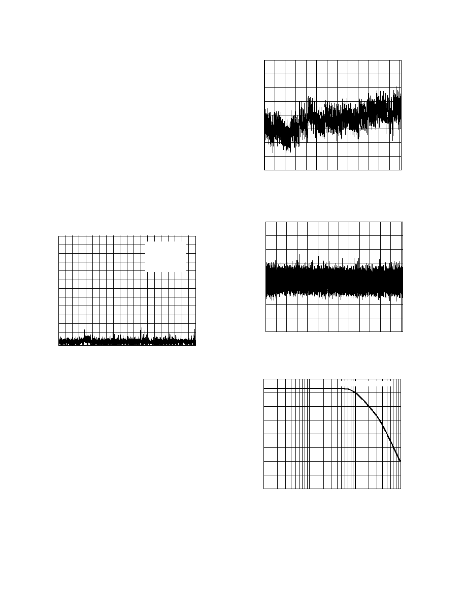
FREQUENCY ≠ kHz
0
≠10
≠20
≠30
≠40
≠50
≠60
≠70
≠80
≠90
≠100
≠110
≠125
0
10
20
30
40
50
60
70
80
90
100
AMPLITUDE ≠ dB
5
15
25
35
45
55
65
75
85
95
5280 POINT FFT
f
SAMPLE
= 200kHz
f
IN
= 20kHz
SNRD = 86.7dB
THD = 100.7dB
Figure 16. FFT Plot
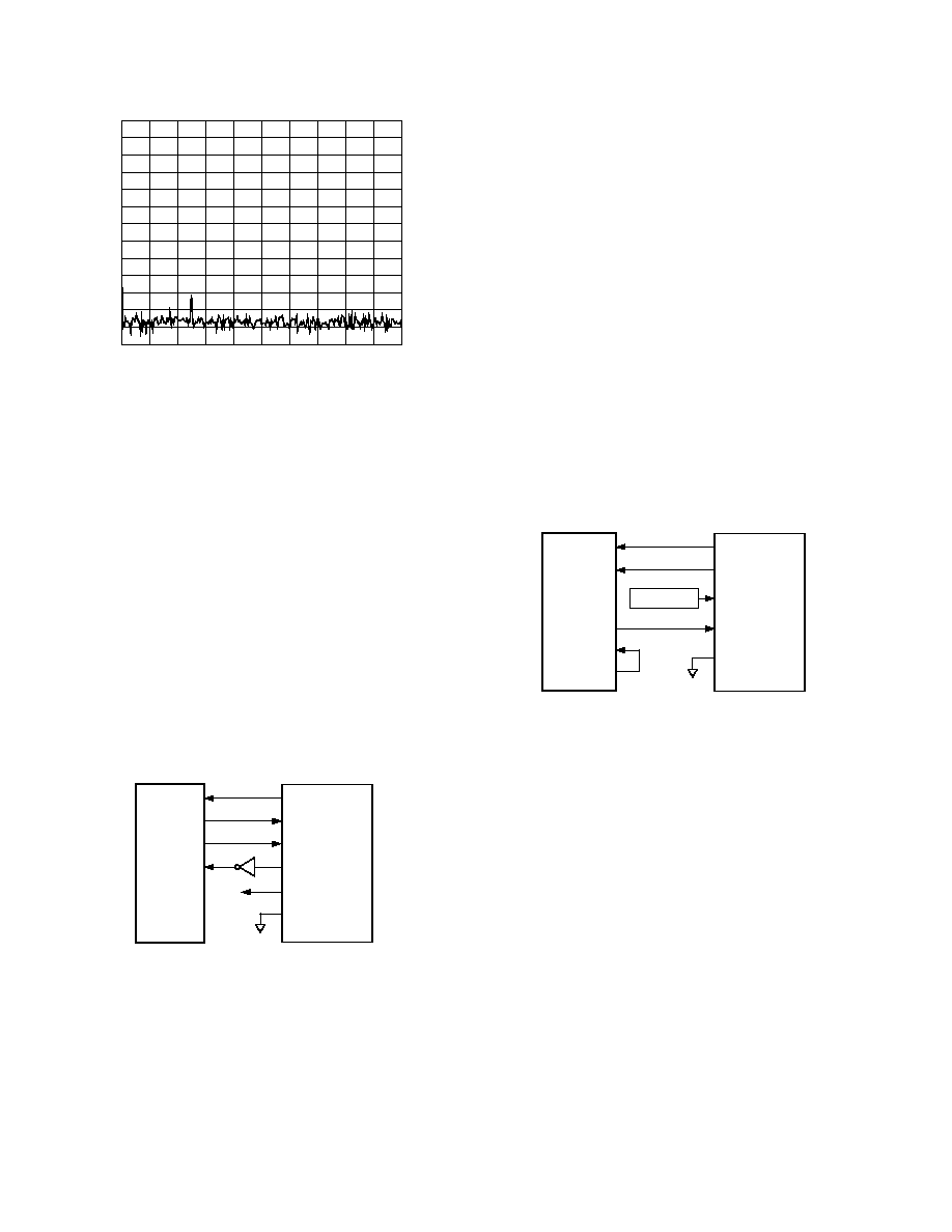
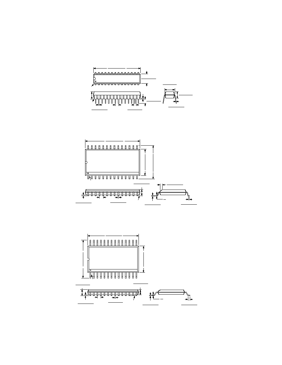
DC PERFORMANCE
The factory calibration scheme used for the AD974 compen-
sates for bit weight errors that may exist in the capacitor array.
The mismatch in capacitor values is adjusted (using the calibra-
tion coefficients) during a conversion, resulting in excellent dc
linearity performance. Figures 17 and 18, respectively, show
typical INL and DNL plots for the AD974 at +25
∞
C.
A histogram test is a statistical method for deriving an A/D
converter's differential nonlinearity. A ramp input is sampled
by the ADC and a large number of conversions are taken at
each voltage level, averaged and then stored. The effect of
averaging is to reduce the transition noise by 1/n. If 64 samples
are averaged at each point, the effect of transition noise is
reduced by a factor of 8; i.e., a transition noise of 0.8 LSBs rms
is reduced to 0.1 LSBs rms. Theoretically the codes, during a
test of DNL, would all be the same size and therefore have an
equal number of occurrences. A code with an average number
of occurrences would have a DNL of "0." A code that is
different from the average would have a DNL that was either
greater or less than zero LSB. A DNL of ≠1 LSB indicates that
there is a missing code present at the 16-bit level and that the
ADC exhibits 15-bit performance.
SAMPLES ≠ K
2.0
1.5
1.0
0.5
0
≠0.5
≠1.0
≠1.5
≠2.0
0
5
10
15
20
25
30
35
40
45
50
55
60
66
100%
Figure 17. INL Plot
SAMPLES ≠ K
2.0
1.5
1.0
0.5
0
≠0.5
≠1.0
≠1.5
≠2.0
0
5
10
15
20
25
30
35
40
45
50
55
60
66
100%
Figure 18. DNL Plot
INPUT SIGNAL FREQUENCY ≠ kHz
90
1
1000
100
10
80
70
60
50
40
30
20
10
SNR+D (dB) FOR AD974
SINAD (dB) FOR V
IN
= 0dB
Figure 19. S/(N+D) vs. Input Frequency
REV. A
AD974
≠17≠
TEMPERATURE ≠ C
110
80
≠75
150
≠50
≠25
0
25
50
75
100
125
105
100
95
90
85
≠80
≠110
≠85
≠90
≠95
≠100
≠105
SFDR, S/N + D ≠ dB
SNRD
SFDR
THD
THD ≠ dB
Figure 20. AC Parameters vs. Temperature
DC CODE UNCERTAINTY
Ideally, a fixed dc input should result in the same output code
for repetitive conversions; however, as a consequence of un-
avoidable circuit noise within the wideband circuits of the ADC,
a range of output codes may occur for a given input voltage.
Thus, when a dc signal is applied to the AD974 input, and
10,000 conversions are recorded, the result will be a distribution
of codes as shown in Figure 21. This histogram shows a bell
shaped curve consistent with the Gaussian nature of thermal
noise. The histogram is approximately seven codes wide. The
standard deviation of this Gaussian distribution results in a code
transition noise of 1 LSB rms.
4000
0
≠3
≠2
≠1
0
1
2
3
4
3500
2000
1500
1000
500
3000
2500
Figure 21. Histogram of 10,000 Conversions of a DC Input
POWER-DOWN FEATURE
The AD974 has analog and reference power-down capability
through the PWRD pin. When the PWRD pin is taken high,
the power consumption drops from a maximum value of
100 mW to a typical value of 50
µ
W. When in the power-
down mode the previous conversion results are still available in
the internal registers and can be read out providing it has not
already been shifted out.
When used with an external reference, connected to the REF
pin and a 2.2
µ
F capacitor, connected to the CAP pin, the
power-up recovery time is typically 1 ms. This typical value of
1 ms for recovery time depends on how much charge has de-
cayed from the external 2.2
µ
F capacitor on the CAP pin and
assumes that it has decayed to zero. The 1 ms recovery time has
been specified such that settling to 16 bits has been achieved.
When used with the internal reference, the dominant time con-
stant for power-up recovery is determined by the external ca-
pacitor on the REF pin and the internal 4K impedance seen at
that pin. An external 2.2
µ
F capacitor is recommended for the
REF pin.
CROSSTALK
The crosstalk between adjacent channels, nonadjacent channels
and worst-case adjacent channels is shown in Figures 22 to 24.
The worst-case crosstalk occurs between channels 1 and 2.
≠80
≠115
1
10
100
1000
≠95
≠100
≠105
≠110
≠85
≠90
10000
ACTIVE CHANNEL INPUT FREQUENCY ≠ kHz
RESULTING AMPLITUDE ON SELECTED
CHANNEL (dB) WITH INPUT GROUNDED
ADJACENT CHANNELS,
WORST PAIR
NONADJACENT
CHANNELS
Figure 22. Crosstalk vs. Input Frequency (kHz)
0
≠130
1
2
≠90
≠100
≠110
≠120
≠70
≠80
FREQUENCY ≠ kHz
dBFS
4
6
8
10
12
14
16
18
20
≠60
≠40
≠50
≠30
≠10
≠20
Figure 23. Adjacent Channel Crosstalk, Worst Pair
(8192 Point FFT; AIN 2 = 1.02 kHz, ≠0.1 dB; AIN 1 = AGND)
REV. A
AD974
≠18≠
0
≠130
1
2
≠90
≠100
≠110
≠120
≠70
≠80
FREQUENCY ≠ kHz
dBFS
4
6
8
10
12
14
16
18
20
≠60
≠40
≠50
≠30
≠10
≠20
Figure 24. Adjacent Channel Crosstalk, Worst Pair (8192
Point FFT; AIN 2 = 220 kHz, ≠0.1 dB; AIN 1 = AGND)
MICROPROCESSOR INTERFACING
The AD974 is ideally suited for traditional dc measurement
applications supporting a microprocessor, and ac signal process-
ing applications interfacing to a digital signal processor. The
AD974 is designed to interface with a general purpose serial
port or I/O ports on a microcontroller. A variety of external
buffers can be used with the AD974 to prevent digital noise
from coupling into the ADC. The following sections illustrate
the use of the AD974 with an SPI equipped microcontroller and
the ADSP-2181 signal processor.
SPI INTERFACE
Figure 25 shows a general interface diagram between the
AD974 and an SPI equipped microcontroller. This interface
assumes that the convert pulses will originate from the micro-
controller and that the AD974 will act as the slave device. The
convert pulse could be initiated in response to an internal timer
interrupt. The reading of output data, one byte at a time,
if necessary, could be initiated in response to the end-of-
conversion signal (
BUSY going high).
+5V
SDI
SCK
I/O PORT
IRQ
SPI
DATA
DATACLK
R/
C
BUSY
EXT/
INT
CS
AD974
Figure 25. AD974-to-SPI Interface
ADSP-2181 INTERFACE
Figure 26 shows an interface between the AD974 and the
ADSP-2181 Digital Signal Processor. The AD974 is configured
for the Internal Clock mode (EXT/
INT = 0) and will therefore
act as the master device. The convert command is shown gener-
ated from an external oscillator in order to provide a low jitter
signal appropriate for both dc and ac measurements. Because
the SPORT, within the ADSP-2181, will be seeing a discontinu-
ous external clock, some steps are required to ensure that the
serial port is properly synchronized to this clock during each
data read operation. The recommended procedure to ensure
this is as follows:
∑ Enable SPORT0 through the System Control register.
∑ Set the SCLK Divide register to zero.
∑ Setup PF0 and PF1 as outputs by setting bits 0 and 1 in
PFTYPE.
∑ Force RFS0 low through PF0. The Receive Frame Sync
signal has been programmed active high.
∑ Enable AD974 by forcing
CS = 0 through PF1.
∑ Enable SPORT0 Receive Interrupt through the IMASK
register.
∑ Wait for at least one full conversion cycle of the AD974 and
throw away the received data.
∑ Disable the AD974 by forcing
CS = 1 through PF1.
∑ Wait for a period of time equal to one conversion cycle.
∑ Force RFS0 high through PF0.
∑ Enable the AD974 by forcing
CS = 0 through PF1.
The ADSP-2181 SPORT0 will now remain synchronized to the
external discontinuous clock for all subsequent conversions.
DR0
SCLK0
PF1
RFS0
ADSP-2181
DATA
DATACLK
R/
C
EXT/
INT
CS
AD974
PF0
OSCILLATOR
SPORT0 CNTRL REG = 0 300F
Figure 26. AD974-to-ADSP-2181 Interface
POWER SUPPLIES AND DECOUPLING
The AD974 has two power supply input pins. V
ANA
and V
DIG
provide the supply voltages to the analog and digital portions,
respectively. V
ANA
is the +5 V supply for the on-chip analog
circuitry, and V
DIG
is the +5 V supply for the on-chip digital
circuitry. The AD974 is designed to be independent of power
supply sequencing and thus free from supply voltage induced
latchup.
With high performance linear circuits, changes in the power
supplies can result in undesired circuit performance. Optimally,
well regulated power supplies should be chosen with less than
1% ripple. The ac output impedance of a power supply is a
complex function of frequency and will generally increase with
frequency. Thus, high frequency switching, such as that en-
countered with digital circuitry, requires the fast transient cur-
rents that most power supplies cannot adequately provide. Such
a situation results in large voltage spikes on the supplies. To
compensate for the finite ac output impedance of most supplies,
charge "reserves" should be stored in bypass capacitors. This
will effectively lower the supplies impedance presented to the
AD974 V
ANA
and V
DIG
pins and reduce the magnitude of these
spikes. Decoupling capacitors, typically 0.1
µ
F, should be placed
close to the power supply pins of the AD974 to minimize any
inductance between the capacitors and the V
ANA
and V
DIG
pins.

REV. A
AD974
≠19≠
The AD974 may be operated from a single +5 V supply.
When separate supplies are used, however, it is beneficial to
have larger (10
µ
F) capacitors placed between the logic supply
(V
DIG
) and digital common (DGND), and between the analog
supply (V
ANA
) and the analog common (AGND2). Addition-
ally, 10
µ
F capacitors should be located in the vicinity of the
ADC to further reduce low frequency ripple. In systems where
the device will be subjected to harsh environmental noise,
additional decoupling may be required.
GROUNDING
The AD974 has three ground pins; AGND1, AGND2 and
DGND. The analog ground pins are the "high quality" ground
reference points and should be connected to the system analog
common. AGND2 is the ground to which most internal ADC
analog signals are referenced. This ground is most susceptible to
current-induced voltage drops and thus must be connected with
the least resistance back to the power supply. AGND1 is the low
current analog supply ground and should be the analog common
for the external reference, input op amp drive circuitry and the
input resistor divider circuit. By applying the inputs referenced
to this ground, any ground variations will be offset and have a
minimal effect on the resulting analog input to the ADC. The
digital ground pin, DGND, is the reference point for all of the
digital signals that control the AD974.
The AD974 can be powered with two separate power supplies or
with a single analog supply. When the system digital supply is
noisy, or fast switching digital signals are present, it is recom-
mended to connect the analog supply to both the V
ANA
and V
DIG
pins of the AD974 and the system supply to the remaining
digital circuitry. With this configuration, AGND1, AGND2 and
DGND should be connected back at the ADC. When there is
significant bus activity on the digital output pins, the digital and
analog supply pins on the ADC should be separated. This would
eliminate any high speed digital noise from coupling back to the
analog portion of the AD974. In this configuration, the digital
ground pin DGND should be connected to the system digital
ground and be separate from the AGND pins.
BOARD LAYOUT
Designing with high resolution data converters requires careful
attention to board layout and trace impedance is a significant
issue. A 1.22 mA current through a 0.5
trace will develop a
voltage drop of 0.6 mV, which is 2 LSBs at the 16-bit level over
the 20 volt full-scale range. Ground circuit impedances should
be reduced as much as possible since any ground potential
differences between the signal source and the ADC appear as
an error voltage in series with the input signal. In addition to
ground drops, inductive and capacitive coupling needs to be
considered. This is especially true when high accuracy analog
input signals share the same board with digital signals. Thus, to
minimize input noise coupling, the input signal leads to V
IN
and
the signal return leads from AGND should be kept as short as
possible. In addition, power supplies should also be decoupled
to filter out ac noise.
Analog and digital signals should not share a common path.
Each signal should have an appropriate analog or digital return
routed close to it. Using this approach, signal loops enclose a
small area, minimizing the inductive coupling of noise. Wide
PC tracks, large gauge wire and ground planes are highly rec-
ommended to provide low impedance signal paths. Separate
analog and digital ground planes are also recommended with a
single interconnection point to minimize ground loops. Analog
signals should be routed as far as possible from high speed
digital signals and if absolutely necessary, should only cross
them at right angles.
In addition, it is recommended that multilayer PC boards be
used with separate power and ground planes. When designing
the separate sections, careful attention should be paid to the
layout.
REV. A
AD974
≠20≠
OUTLINE DIMENSIONS
Dimensions shown in inches and (mm).
C3273a≠0≠5/99
PRINTED IN U.S.A.
28-Lead 300 Mil Plastic DIP
(N-28B)
28
1
14
15
PIN 1
1.425 (38.195)
1.385 (35.179)
0.280 (7.11)
0.240 (6.10)
0.325 (8.25)
0.300 (7.62)
0.195 (4.95)
0.115 (2.93)
0.014 (0.356)
0.008 (0.204)
SEATING
PLANE
0.150 (3.81)
0.115 (2.92)
0.022 (0.558)
0.014 (0.356)
0.070 (1.77)
0.045 (1.15)
0.015 (0.381)
MIN
0.100 (2.54)
BSC
0.210
(5.33)
MAX
28-Lead Wide Body (SOIC)
(R-28)
0.0192 (0.49)
0.0138 (0.35)
SEATING
PLANE
0.0118 (0.30)
0.0040 (0.10)
0.1043 (2.65)
0.0926 (2.35)
0.0500
(1.27)
BSC
0.4193 (10.65)
0.3937 (10.00)
0.2992 (7.60)
0.2914 (7.40)
0.7125 (18.10)
0.6969 (17.70)
PIN 1
28
15
14
1
0.0125 (0.32)
0.0091 (0.23)
0.0500 (1.27)
0.0157 (0.40)
8∞
0∞
0.0291 (0.74)
0.0098 (0.25)
x 45∞
28-Lead Shrink Small Outline Package (SSOP)
(RS-28)
8∞
0∞
0.009 (0.229)
0.005 (0.127)
0.03 (0.762)
0.022 (0.558)
SEATING
PLANE
0.008 (0.203)
0.002 (0.050)
0.07 (1.79)
0.066 (1.67)
0.0256
(0.65)
BSC
0.078 (1.98)
0.068 (1.73)
0.015 (0.38)
0.010 (0.25)
0.311 (7.9)
0.301 (7.64)
28
15
14
1
0.407 (10.34)
0.397 (10.08)
0.212 (5.38)
0.205 (5.21)
PIN 1