 | –≠–ª–µ–∫—Ç—Ä–æ–Ω–Ω—ã–π –∫–æ–º–ø–æ–Ω–µ–Ω—Ç: AD9777 | –°–∫–∞—á–∞—Ç—å:  PDF PDF  ZIP ZIP |
Document Outline
- AD9777 16-BIT, 160 MSPS 2X/4X/8X INTERPOLATING DUAL TxDAC +Æ D/A CONVERTER
- FEATURES
- APPLICATIONS
- GENERAL DESCRIPTION
- PRODUCT HIGHLIGHTS
- AD9777ÖSPECIFICATIONS
- ABSOLUTE MAXIMUM RATINGS
- ORDERING GUIDE
- THERMAL CHARACTERISTICS
- PIN CONFIGURATION
- PIN FUNCTION DESCRIPTIONS
- DIGITAL FILTER SPECIFICATIONS
- DEFINITIONS OF SPECIFICATIONS
- Typical Performance Characteristics
- MODE CONTROL (via SPI Port)
- REGISTER DESCRIPTION
- FUNCTIONAL DESCRIPTION
- SERIAL INTERFACE FOR REGISTER CONTROL
- GENERAL OPERATION of the SERIAL INTERFACE
- INSTRUCTION BYTE
- R/W
- N1, N0
- A4, A3, A2, A1, A0
- SERIAL INTERFACE PORT PIN DESCRIPTIONS
- MSB/LSB TRANSFERS
- NOTES ON SERIAL PORT OPERATION
- DAC OPERATION
- 1R/2R MODE
- CLOCK INPUT CONFIGURATIONS
- PROGRAMMABLE PLL
- POWER DISSIPATION
- SLEEP/POWER-DOWN MODES
- ONE/TWO PORT INPUT MODES
- PLL ENABLED, TWO PORT MODE
- DATACLK INVERSION
- DATACLK DRIVER STRENGTH
- PLL ENABLED, ONE PORT MODE
- ONEPORTCLK INVERSION
- ONEPORTCLK DRIVER STRENGTH
- IQ PAIRING
- PLL DISABLED, TWO PORT MODE
- PLL DISABLED, ONE PORT MODE
- DIGITAL FILTER MODES
- AMPLITUDE MODULATION
- MODULATION, NO INTERPOLATION
- MODULATION, INTERPOLATION = 2X
- MODULATION, INTERPOLATION = 4X
- MODULATION, INTERPOLATION = 8X
- ZERO STUFFING
- INTERPOLATING (COMPLEX MIX MODE)
- OPERATIONS ON COMPLEX SIGNALS
- COMPLEX MODULATION AND IMAGE REJECTION OF BASEBAND SIGNALS
- IMAGE REJECTION AND SIDEBAND SUPPRESSION OF MODULATED CARRIERS
- Region A
- Region B
- Region C
- Region D
- APPLYING THE AD9777 OUTPUT CONFIGURATIONS
- UNBUFFERED DIFFERENTIAL OUTPUT, EQUIVALENT CIRCUIT
- DIFFERENTIAL COUPLING USING A TRANSFORMER
- DIFFERENTIAL COUPLING USING AN OP AMP
- INTERFACING THE AD9777 WITH THE AD8345 QUADRATURE MODULATOR
- EVALUATION BOARD
- TEST CONFIGURATIONS
- CIRCUITRY
- EVALUATION BOARD COMPONENTS
- EVALUATION BOARD LAYOUT
- OUTLINE DIMENSIONS
REV. 0
a
Information furnished by Analog Devices is believed to be accurate and
reliable. However, no responsibility is assumed by Analog Devices for its
use, nor for any infringements of patents or other rights of third parties that
may result from its use. No license is granted by implication or otherwise
under any patent or patent rights of Analog Devices.
One Technology Way, P.O. Box 9106, Norwood, MA 02062-9106, U.S.A.
Tel: 781/329-4700
www.analog.com
Fax: 781/326-8703
© Analog Devices, Inc., 2002
AD9777
*
16-Bit, 160 MSPS 2 /4 /8
Interpolating Dual TxDAC+
Æ
D/A Converter
FEATURES
16-Bit Resolution, 160/400 MSPS Input/Output Data Rate
Selectable 2 /4 /8 Interpolating Filter
Programmable Channel Gain and Offset Adjustment
f
S
/4, f
S
/8 Digital Quadrature Modulation
Capability
Direct IF Transmission Mode for 70 MHz + IFs
Enables Image Rejection Architecture
Fully Compatible SPI Port
Excellent AC Performance
SFDR ≠73 dBc @ 2 MHz≠35 MHz
WCDMA ACPR 71 dB @ IF = 71 MHz
Internal PLL Clock Multiplier
Selectable Internal Clock Divider
Versatile Clock Input
Differential/Single-Ended Sine Wave or
TTL/CMOS/LVPECL Compatible
Versatile Input Data Interface
Two's Complement/Straight Binary Data Coding
Dual-Port or Single-Port Interleaved Input Data
Single 3.3 V Supply Operation
Power Dissipation: Typical 1.2 W @ 3.3 V
On-Chip 1.2 V Reference
80-Lead Thermally Enhanced TQFP Package
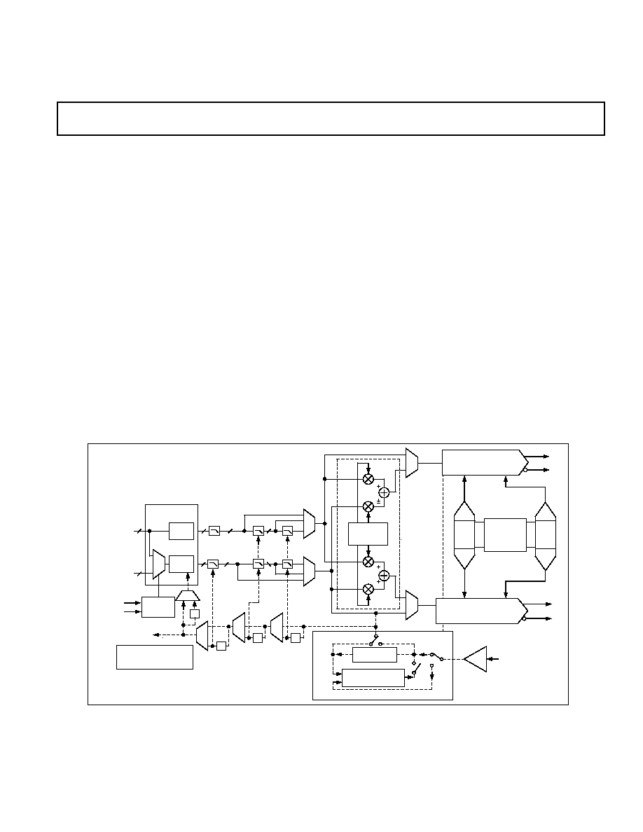
FUNCTIONAL BLOCK DIAGRAM
DIFFERENTIAL
CLK
COS
SIN
HALF-
BAND
FILTER 1
16
IMAGE
REJECTION/
DUAL DAC
MODE
BYPASS
MUX
I AND Q
NONINTERLEAVED
OR
INTERLEAVED
DATA
WRITE
SELECT
CLOCK OUT
HALF-BAND FILTERS ALSO CAN BE
CONFIGURED FOR "ZERO STUFFING ONLY"
*
GAIN
DAC
OFFSET
DAC
f
DAC
/2, 4, 8
SIN
COS
I/Q DAC
GAIN/OFFSET
REGISTERS
IOFFSET
VREF
(
f
DAC
)
PHASE DETECTOR
AND VCO
PRESCALER
PLL CLOCK MULTIPLIER AND CLOCK DIVIDER
16
16
/2
16
DATA
ASSEMBLER
16
16
16
16
16
16
MUX
CONTROL
/2
/2
I
LATCH
Q
LATCH
/2
HALF-
BAND
FILTER 2
HALF-
BAND
FILTER 3
*
*
*
AD9777
SPI INTERFACE AND
CONTROL REGISTERS
FILTER
BYPASS
MUX
IDAC
IDAC
I
OUT
GENERAL DESCRIPTION
The AD9777 is the 16-bit member of the AD977x pin compatible,
high performance, programmable 2
◊/4◊/8◊ interpolating TxDAC+
family. The AD977x family features a serial port interface (SPI)
providing a high level of programmability, thus allowing for
enhanced system level options. These options include: selectable
2
◊/4◊/8◊ interpolation filters; f
S
/2, f
S
/4, or f
S
/8 digital quadrature
modulation with image rejection; a direct IF mode; programmable
channel gain and offset control; programmable internal clock
divider; straight binary or two's complement data interface; and
a single-port or dual-port data interface.
The selectable 2
◊/4◊/8◊ interpolation filters simplify the require-
ments of the reconstruction filters while simultaneously enhancing
the TxDAC+ family's pass-band noise/distortion performance.
The independent channel gain and offset adjust registers allow
the user to calibrate LO feedthrough and sideband suppression
(continued on page 2)
APPLICATIONS
Communications
Analog Quadrature Modulation Architectures
3G, Multicarrier GSM, TDMA, CDMA Systems
Broadband Wireless, Point-to-Point Microwave Radios
Instrumentation/ATE
TxDAC+ is a registered trademark of Analog Devices, Inc.
*Protected by U.S. Patent Numbers, 5568145, 5689257, and 5703519. Other patents pending.

REV. 0
≠2≠
AD9777
(continued from page 1)
errors associated with analog quadrature modulators. The 6 dB
of gain adjustment range can also be used to control the output
power level of each DAC.
The AD9777 features the ability to perform f
S
/2, f
S
/4, and f
S
/8
digital modulation and image rejection when combined with an
analog quadrature modulator. In this mode, the AD9777 accepts
I and Q complex data (representing a single or multicarrier wave-
form), generates a quadrature modulated IF signal along with its
orthogonal representation via its dual DACs, and presents these
two reconstructed orthogonal IF carriers to an analog quadrature
modulator to complete the image rejection upconversion process.
Another digital modulation mode (i.e., the Direct IF Mode)
allows the original baseband signal representation to be frequency
translated such that pairs of images fall at multiples of one-half
the DAC update rate.
The AD977x family includes a flexible clock interface accepting
differential or single-ended sine wave or digital logic inputs. An
internal PLL clock multiplier is included and generates the
necessary on-chip high frequency clocks. It can also be disabled
to allow the use of a higher performance external clock source. An
internal programmable divider simplifies clock generation in the
converter when using an external clock source. A flexible data
input interface allows for straight binary or two's complement
formats and supports single-port interleaved or dual-port data.
Dual high performance DAC outputs provide a differential
current output programmable over a 2 mA to 20 mA range. The
AD9777 is manufactured on an advanced 0.35 micron CMOS
process, operates from a single supply of 3.1 V to 3.5 V, and
consumes 1.2 W of power.
Targeted at wide dynamic range, multicarrier and multistandard
systems, the superb baseband performance of the AD9777 is
ideal for wideband CDMA, multicarrier CDMA, multicarrier
TDMA, multicarrier GSM, and high performance systems
employing high order QAM modulation schemes. The image
rejection feature simplifies and can help to reduce the number
of signal band filters needed in a transmit signal chain. The
direct IF mode helps to eliminate a costly mixer stage for a
variety of communications systems.
PRODUCT HIGHLIGHTS
1.
The AD9777 is the 16-bit member of the AD977x pin-
compatible, high performance, programmable 2
◊ /4◊/8◊
interpolating TxDAC+ family.
2.
Direct IF transmission is possible for 70 MHz + IFs through
a novel digital mixing process.
3.
f
S
/2, f
S
/4, and f
S
/8 digital quadrature modulation and
user-selectable image rejection simplify/remove cascaded
SAW filter stages.
4.
A 2
◊/4◊/8◊ user-selectable interpolating filter eases data
rate and output signal reconstruction filter requirements.
5.
User-selectable two's complement/straight binary data
coding.
6.
User programmable channel gain control over 1 dB range
in 0.01 dB increments.
7.
User-programmable channel offset control
± 10% over
the FSR.
8.
Ultra high speed 400 MSPS DAC conversion rate.
9.
Internal clock divider provides data rate clock for easy
interfacing.
10.
Flexible clock input with single-ended or differential input,
CMOS, or 1 V p-p LO sine wave input capability.
11.
Low power: Complete CMOS DAC operates on 1.2 W
from a 3.1 V to 3.5 V single supply. The 20 mA full-scale
current can be reduced for lower power operation, and
several sleep functions are provided to reduce power during
idle periods.
12.
On-chip voltage reference: The AD9777 includes a 1.20 V
temperature compensated band gap voltage reference.
13.
80-lead thermally enhanced TQFP.

REV. 0
AD9777
≠3≠
DC SPECIFICATIONS
Parameter
Min
Typ
Max
Unit
RESOLUTION
16
Bits
DC Accuracy
1
Integral Nonlinearity
±6
LSB
Differential Nonlinearity
≠6.5
±3
+6.5
LSB
ANALOG OUTPUT (for 1R and 2R Gain Setting Modes)
Offset Error
≠0.025
±0.01
+0.025
% of FSR
Gain Error (with Internal Reference)
≠1.0
+1.0
% of FSR
Gain Matching
≠1
±0.1
+1
% of FSR
Full-Scale Output Current
2
2
20
mA
Output Compliance Range
≠1.0
+1.25
V
Output Resistance
200
k
Output Resistance
3
pF
Gain, Offset Cal DACs, Monotonicity Guaranteed
REFERENCE OUTPUT
Reference Voltage
1.14
1.20
1.26
V
Reference Output Current
3
100
nA
REFERENCE INPUT
Input Compliance Range
0.1
1.25
V
Reference Input Resistance (REFLO = 3 V)
10
M
Small Signal Bandwidth
0.5
MHz
TEMPERATURE COEFFICIENTS
Offset Drift
0
ppm of FSR/
∞C
Gain Drift (With Internal Reference)
50
ppm of FSR/
∞C
Reference Voltage Drift
ppm/
∞C
POWER SUPPLY
AVDD
Voltage Range
3.1
3.3
3.5
V
Analog Supply Current (I
AVDD
)
4
72.5
76
mA
I
AVDD
in SLEEP Mode
23.3
26
mA
CLKVDD (PLL OFF)
Voltage Range
3.1
3.3
3.5
V
Clock Supply Current (I
CLKVDD
)
4
8.5
mA
CLKVDD (PLL ON)
Clock Supply Current (I
CLKVDD
)
23.5
mA
DVDD
Voltage Range
3.1
3.3
3.5
V
Digital Supply Current (I
DVDD
)
4
34
41
mA
Nominal Power Dissipation
4
380
410
mW
P
DIS
5
1.75
W
P
DIS
in PWDN
6.0
mW
Power Supply Rejection Ratio--AVDD
±0.4
% of FSR/V
OPERATING RANGE
≠40
+85
∞C
NOTES
1
Measured at I
OUTA
driving a virtual ground.
2
Nominal full-scale current, I
OUTFS
, is 32
◊ the I
REF
current.
3
Use an external amplifier to drive any external load.
4
100 MSPS f
DAC
with f
OUT
= 1 MHz, all supplies = 3.3 V, no interpolation, no modulation.
5
400 MSPS f
DAC
, f
DATA
= 50 MSPS, f
S
/2 modulation, PLL enabled.
Specifications subject to change without notice.
(T
MIN
to T
MAX
, AVDD = 3.3 V, CLKVDD = 3.3 V, DVDD = 3.3 V, PLLVDD = 3.3 V, I
OUTFS
= 20 mA, unless
otherwise noted.)
AD9777≠SPECIFICATIONS

REV. 0
≠4≠
AD9777
DYNAMIC SPECIFICATIONS
Parameter
Min
Typ
Max
Unit
DYNAMIC PERFORMANCE
Maximum DAC Output Update Rate (f
DAC
)
400
MSPS
Output Settling Time (t
ST
) (to 0.025%)
11
ns
Output Rise Time (10% to 90%)
*
0.8
ns
Output Fall Time (10% to 90%)
*
0.8
ns
Output Noise (I
OUTFS
= 20 mA)
50
pA
Hz
AC LINEARITY--BASEBAND MODE
Spurious-Free Dynamic Range (SFDR) to Nyquist (f
OUT
= 0 dBFS)
f
DATA
= 100 MSPS, f
OUT
= 1 MHz
71
85
dBc
f
DATA
= 65 MSPS, f
OUT
= 1 MHz
85
dBc
f
DATA
= 65 MSPS, f
OUT
= 15 MHz
84
dBc
f
DATA
= 78 MSPS, f
OUT
= 1 MHz
85
dBc
f
DATA
= 78 MSPS, f
OUT
= 15 MHz
83
dBc
f
DATA
= 160 MSPS, f
OUT
= 1 MHz
85
dBc
f
DATA
= 160 MSPS, f
OUT
= 15 MHz
83
dBc
Spurious-Free Dynamic Range within a 1 MHz Window
(f
OUT
= 0 dBFS, f
DATA
= 100 MSPS, f
OUT
= 1 MHz)
73
99.1
Two-Tone Intermodulation (IMD) to Nyquist (f
OUT1
= f
OUT2
= ≠6 dBFS)
f
DATA
= 65 MSPS, f
OUT1
= 10 MHz; f
OUT2
= 11 MHz
85
dBc
f
DATA
= 65 MSPS, f
OUT1
= 20 MHz; f
OUT2
= 21 MHz
78
dBc
f
DATA
= 78 MSPS, f
OUT1
= 10 MHz; f
OUT2
= 11 MHz
85
dBc
f
DATA
= 78 MSPS, f
OUT1
= 20 MHz; f
OUT2
= 21 MHz
78
dBc
f
DATA
= 160 MSPS, f
OUT1
= 10 MHz; f
OUT2
= 11 MHz
85
dBc
f
DATA
= 160 MSPS, f
OUT1
= 20 MHz; f
OUT2
= 21 MHz
84
dBc
Total Harmonic Distortion (THD)
f
DATA
= 100 MSPS, f
OUT
= 1 MHz; 0 dBFS
≠71
≠83
dB
Signal-to-Noise Ratio (SNR)
f
DATA
= 78 MSPS, f
OUT
= 5 MHz; 0 dBFS
79
dB
f
DATA
= 160 MSPS, f
OUT
= 5 MHz; 0 dBFS
75
dB
Adjacent Channel Power Ratio (ACLR)
WCDMA with MHz BW, MHz Channel Spacing
IF = Baseband, f
DATA
= 76.8 MSPS
77
dBc
IF = 19.2 MHz, f
DATA
= 76.8 MSPS
73
dBc
Four-Tone Intermodulation
21 MHz, 22 MHz, 23 MHz, and 24 MHz at ≠12 dBFS
76
dBFS
(f
DATA
= MSPS, Missing Center)
AC LINEARITY--IF MODE
Four-Tone Intermodulation at IF = 200 MHz
201 MHz, 202 MHz, 203 MHz, and 204 MHz at ≠12 dBFS
72
dBFS
(f
DATA
= 160 MSPS, f
DAC
= 320 MHz)
*Measured single ended into 50
load.
Specifications subject to change without notice.
(T
MIN
to T
MAX
, AVDD = 3.3 V, CLKVDD = 3.3 V, DVDD = 3.3 V, PLLVDD = 0 V, I
OUTFS
= 20 mA,
Interpolation = 2 , Differential Transformer Coupled Output, 50
Doubly Terminated,
unless otherwise noted.)
REV. 0
AD9777
≠5≠
CAUTION
ESD (electrostatic discharge) sensitive device. Electrostatic charges as high as 4000 V readily
accumulate on the human body and test equipment and can discharge without detection. Although the
AD9777 features proprietary ESD protection circuitry, permanent damage may occur on devices
subjected to high energy electrostatic discharges. Therefore, proper ESD precautions are recommended
to avoid performance degradation or loss of functionality.
WARNING!
ESD SENSITIVE DEVICE
DIGITAL SPECIFICATIONS
Parameter
Min
Typ
Max
Unit
DIGITAL INPUTS
Logic "1" Voltage
2.1
3
V
Logic "0" Voltage
0
0.9
V
Logic "1" Current
≠10
+10
µA
Logic "0" Current
≠10
+10
µA
Input Capacitance
5
pF
CLOCK INPUTS
Input Voltage Range
0
3
V
Common-Mode Voltage
0.75
1.5
2.25
V
Differential Voltage
0.5
1.5
V
Specifications subject to change without notice.
(T
MIN
to T
MAX
, AVDD = 3.3 V, CLKVDD = 3.3 V, PLLVDD = 0 V, DVDD = 3.3 V, I
OUTFS
= 20 mA, unless
otherwise noted.)
ABSOLUTE MAXIMUM RATINGS
*
Parameter
With Respect to
Min
Max
Unit
AVDD, DVDD, CLKVDD
AGND, DGND, CLKGND
≠0.3
+4.0
V
AVDD, DVDD, CLKVDD
AVDD, DVDD, CLKVDD
≠4.0
+4.0
V
AGND, DGND, CLKGND
AGND, DGND, CLKGND
≠0.3
+0.3
V
REFIO, REFLO, FSADJ1/2
AGND
≠0.3
AVDD + 0.3
V
I
OUTA
, I
OUTB
AGND
≠1.0
AVDD + 0.3
V
P1B15≠P1B0, P2B15≠P2B0
DGND
≠0.3
DVDD + 0.3
V
DATACLK, PLL_LOCK
DGND
≠0.3
DVDD + 0.3
V
CLK+, CLK≠, RESET
CLKGND
≠0.3
CLKVDD + 0.3
V
LPF
CLKGND
≠0.3
CLKVDD + 0.3
V
SPI_CSB, SPI_CLK,
DGND
≠0.3
DVDD + 0.3
V
SPI_SDIO, SPI_SDO
Junction Temperature
+125
∞C
Storage Temperature
≠65
+150
∞C
Lead Temperature (10 sec)
+300
∞C
*Stresses above those listed under the ABSOLUTE MAXIMUM RATINGS may cause permanent damage to the device. This is a stress rating only; functional
operation of the device at these or any other conditions above those indicated in the operational sections of this specification is not implied. Exposure to absolute
maximum ratings for extended periods may affect device reliability.
THERMAL CHARACTERISTICS
Thermal Resistance
80-Lead Thermally Enhanced
TQFP Package
JA
= 23.5
∞C/W*
*With thermal pad soldered to PCB.
ORDERING GUIDE
Temperature
Package
Package
Model
Range
Description
Option
*
AD9777BSV
≠40
∞C to +85∞C 80-Lead TQFP
SV-80
AD9777EB
Evaluation Board
*SV = Thin Plastic Quad Flatpack
REV. 0
≠6≠
AD9777
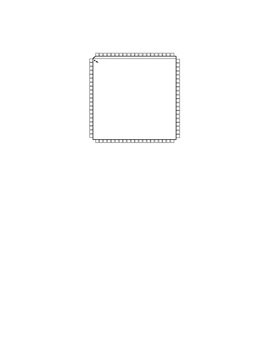
PIN CONFIGURATION
80 79 78 77 76
71 70 69 68 67 66 65
75 74 73 72
64 63 62 61
1
2
3
4
5
6
7
8
9
10
11
13
14
15
16
12
17
18
20
19
21 22 23 24 25 26 27 28 29 30 31 32 33 34 35 36 37 38 39 40
PIN 1
IDENTIFIER
TOP VIEW
(Not to Scale)
60
59
58
57
56
55
54
53
52
51
50
49
48
47
46
45
44
43
42
41
AVDD
AGND
AVDD
AGND
AVDD
AGND
AGND
I
OUTA1
I
OUTB1
AGND
AGND
I
OUTA2
I
OUTB2
AGND
AGND
AVDD
AGND
AVDD
AGND
AVDD
CLKVDD
LPF
CLKVDD
CLKGND
CLK+
CLK≠
DATACLK/PLL_LOCK
DGND
DVDD
P1B15 (MSB)
P1B14
P1B13
P1B12
P1B11
P1B10
DGND
DVDD
P1B9
P1B8
FSADJ1
FSADJ2
REFIO
RESET
SPI_CSB
SPI_CLK
SPI_SDIO
SPI_SDO
DGND
DVDD
P2B0 (LSB)
P2B1
P2B3
P2B4
P2B5
P1B7
P1B6
P1B5
P1B4
DGND
DVDD
P1B3
P1B2
P1B1
P1B0 (LSB)
ONEPORTCLK/P2B14
P2B13
P2B12
DGND
DVDD
IQSEL/P2B15 (MSB)
AD9777
TxDAC+
DGND
DVDD
P2B6
P2B7
P2B11
P2B10
P2B9
P2B8
CLKGND
P2B2

REV. 0
AD9777
≠7≠
PIN FUNCTION DESCRIPTIONS
Pin Number
Mnemonic
Description
1, 3
CLKVDD
Clock Supply Voltage
2
LPF
PLL Loop Filter
4, 7
CLKGND
Clock Supply Common
5
CLK+
Differential Clock Input
6
CLK≠
Differential Clock Input
8
DATACLK/PLL_LOCK
With the PLL enabled, this pin indicates the state of the PLL. A read of a
Logic "1" indicates the PLL is in the locked state. Logic "0" indicates the
PLL has not achieved lock. This pin may also be programmed to act as
either an input or output (Address 02h, Bit 3) DATACLK signal running at
the input data rate.
9, 17, 25, 35, 44, 52
DGND
Digital Common
10, 18, 26, 36, 43, 51
DVDD
Digital Supply Voltage
11≠16, 19≠24, 27≠30
P1B15 (MSB) to P1B0 (LSB) Port "1" Data Inputs
31
IQSEL/P2B15 (MSB)
In "1" port mode, IQSEL = 1 followed by a rising edge of the differential
input clock will latch the data into the I channel input register. IQSEL = 0
will latch the data into the Q channel input register. In "2" port mode, this
pin becomes the port "2" MSB.
32
ONEPORTCLK/P2B14
With the PLL disabled and the AD9777 in "1" port mode, this pin becomes
a clock output that runs at twice the input data rate of the I and Q channels.
This allows the AD9777 to accept and demux interleaved I and Q data to
the I and Q input registers.
33, 34, 37≠42, 45≠50
P2B13 to P2B0 (LSB)
Port "2" Data Inputs
53
SPI_SDO
In the case where SDIO is an input, SDO acts as an output. When SDIO
becomes an output, SDO enters a High-Z state.
54
SPI_SDIO
Bidirectional Data Pin. Data direction is controlled by Bit 7 of Register
Address 00h. The default setting for this bit is "0," which sets SDIO as an input.
55
SPI_CLK
Data input to the SPI port is registered on the rising edge of SPI_CLK.
Data output on the SPI port is registered on the falling edge.
56
SPI_CSB
Chip Select/SPI Data Synchronization. On momentary logic high, resets
SPI port logic and initializes instruction cycle.
57
RESET
Logic "1" resets all of the SPI port registers, including Address 00h, to their
default values. A software reset can also be done by writing a Logic "1" to
SPI Register 00h, Bit 5. However, the software reset has no effect on the bits
in Address 00h.
58
REFIO
Reference Output, 1.2 V Nominal
59
FSADJ2
Full-Scale Current Adjust, Q Channel
60
FSADJ1
Full-Scale Current Adjust, I Channel
61, 63, 65, 76, 78, 80
AVDD
Analog Supply Voltage
62, 64, 66, 67, 70, 71, AGND
Analog Common
74, 75, 77, 79
68, 69
I
OUTA2
, I
OUTB2
Differential DAC Current Outputs, Q Channel
72, 73
I
OUTA1
, I
OUTB1
Differential DAC Current Outputs, I Channel

REV. 0
≠8≠
AD9777
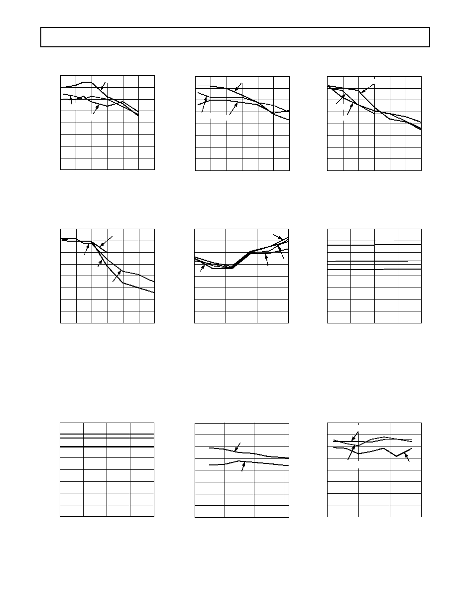
DIGITAL FILTER SPECIFICATIONS
Half-Band Filter No. 1 (43 Coefficients)
Tap
Coefficient
1, 43
8
2, 42
0
3, 41
≠29
4, 40
0
5, 39
67
6, 38
0
7, 37
≠134
8, 36
0
9, 35
244
10, 34
0
11, 33
≠414
12, 32
0
13, 31
673
14, 30
0
15, 29
≠1079
16, 28
0
17, 27
1772
18, 26
0
19, 25
≠3280
20, 24
0
21, 23
10364
22
16384
Half-Band Filter No. 2 (19 Coefficients)
Tap
Coefficient
1, 19
19
2, 18
0
3, 17
≠120
4, 16
0
5, 15
438
6, 14
0
7, 13
≠1288
8, 12
0
9, 11
5047
10
8192
Half-Band Filter No. 3 (11 Coefficients)
Tap
Coefficient
1, 11
7
2, 10
0
3, 9
≠53
4, 8
0
5, 7
302
6
512
f
OUT
≠ Normalized to Input Data Rate
≠120
0
0.5
ATTENUATION ≠ dBFS
≠100
≠80
≠60
≠40
≠20
0
20
1.0
1.5
2.0
Figure 1a. 2 Interpolating Filter Response
f
OUT
≠ Normalized to Input Data Rate
≠120
0
0.5
ATTENUATION ≠ dBFS
≠100
≠80
≠60
≠40
≠20
0
20
1.0
1.5
2.0
Figure 1b. 4 Interpolating Filter Response
f
OUT
≠ Normalized to Input Data Rate
≠120
0
2
ATTENUATION ≠ dBFS
≠100
≠80
≠60
≠40
≠20
0
20
4
6
8
Figure 1c. 8 Interpolating Filter Response

REV. 0
AD9777
≠9≠
DEFINITIONS OF SPECIFICATIONS
Adjacent Channel Power Ratio (ACPR)
A ratio in dBc between the measured power within a channel
relative to its adjacent channel.
Complex Image Rejection
In a traditional two-part upconversion, two images are created
around the second IF frequency. These images are redundant
and have the effect of wasting transmitter power and system
bandwidth. By placing the real part of a second complex modu-
lator in series with the first complex modulator, either the upper
or lower frequency image near the second IF can be rejected.
Complex Modulation
The process of passing the real and imaginary components of a
signal through a complex modulator (transfer function = e
j t
=
cos t + jsin t) and realizing real and imaginary components on
the modulator output.
Differential Nonlinearity (DNL)
DNL is the measure of the variation in analog value, normalized
to full scale, associated with a 1 LSB change in digital input code.
Gain Error
The difference between the actual and ideal output span. The
actual span is determined by the output when all inputs are set
to "1," minus the output when all inputs are set to "0."
Glitch Impulse
Asymmetrical switching times in a DAC give rise to undesired
output transients that are quantified by a glitch impulse. It is
specified as the net area of the glitch in pV≠S.
Group Delay
Number of input clocks between an impulse applied at the
device input and peak DAC output current. A half-band FIR
filter has constant group delay over its entire frequency range.
Impulse Response
Response of the device to an impulse applied to the input.
Interpolation Filter
If the digital inputs to the DAC are sampled at a multiple rate of
f
DATA
(interpolation rate), a digital filter can be constructed that has a
sharp transition band near f
DATA
/2. Images that would typically
appear around f
DAC
(output data rate) can be greatly suppressed.
Linearity Error (Also Called Integral Nonlinearity or INL)
Linearity error is defined as the maximum deviation of the actual
analog output from the ideal output, determined by a straight
line drawn from zero to full scale.
Monotonicity
A D/A converter is monotonic if the output either increases or
remains constant as the digital input increases.
Offset Error
The deviation of the output current from the ideal of "0" is
called offset error. For I
OUTA
, 0 mA output is expected when the
inputs are all "0." For I
OUTB
, 0 mA output is expected when all
inputs are set to "1."
Output Compliance Range
The range of allowable voltage at the output of a current-output
DAC. Operation beyond the maximum compliance limits may
cause either output stage saturation or breakdown, resulting in
nonlinear performance.
Pass Band
Frequency band in which any input applied therein passes
unattenuated to the DAC output.
Power Supply Rejection
The maximum change in the full-scale output as the supplies
are varied from minimum to maximum specified voltages.
Signal-to-Noise Ratio (SNR)
SNR is the ratio of the rms value of the measured output signal
to the rms sum of all other spectral components below the Nyquist
frequency, excluding the first six harmonics and dc. The value
for SNR is expressed in decibels.
Spurious-Free Dynamic Range
The difference, in dB, between the rms amplitude of the output
signal and the peak spurious signal over the specified bandwidth.
Settling Time
The time required for the output to reach and remain within a
specified error band about its final value, measured from the
start of the output transition.
Stop-Band Rejection
The amount of attenuation of a frequency outside the pass band
applied to the DAC, relative to a full-scale signal applied at the
DAC input within the pass band.
Temperature Drift
Temperature drift is specified as the maximum change from the
ambient (25
∞C) value to the value at either T
MIN
or T
MAX
. For
offset and gain drift, the drift is reported in ppm of full-scale
range (FSR) per
∞C. For reference drift, the drift is reported in
ppm per
∞C.
Total Harmonic Distortion (THD)
THD is the ratio of the rms sum of the first six harmonic com-
ponents to the rms value of the measured fundamental. It is
expressed as a percentage or in decibels (dB).
REV. 0
≠10≠
AD9777
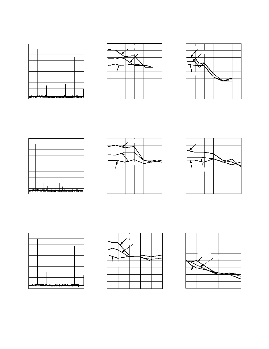
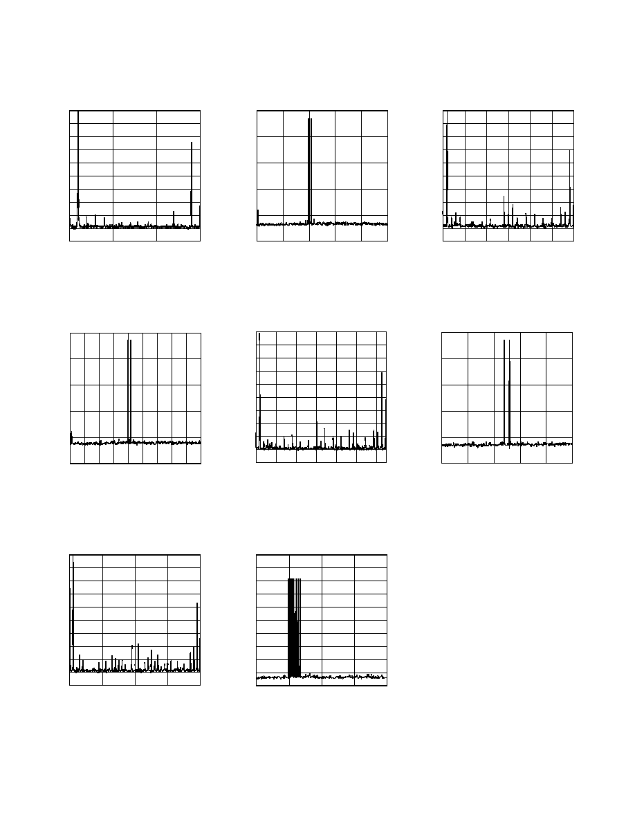
FREQUENCY ≠ MHz
AMPLITUDE ≠ dBm
≠90
0
65
130
≠80
≠70
≠60
≠50
≠40
≠30
≠20
≠10
0
10
TPC 1. Single-Tone Spec-
trum @ f
DATA
= 65 MSPS with
f
OUT
= f
DATA
/3
FREQUENCY ≠ MHz
AMPLITUDE ≠ dBm
≠90
0
50
150
≠80
≠70
≠60
≠50
≠40
≠30
≠20
≠10
0
10
100
TPC 4. Single-Tone Spec-
trum @ f
DATA
= 78 MSPS with
f
OUT
= f
DATA
/3
FREQUENCY ≠ MHz
AMPLITUDE ≠ dBm
≠90
0
100
300
≠80
≠70
≠60
≠50
≠40
≠30
≠20
≠10
0
10
200
TPC 7. Single-Tone Spec-
trum @ f
DATA
= 160 MSPS
with f
OUT
= f
DATA
/3
FREQUENCY ≠ MHz
SFDR ≠ dBc
50
0
20
30
55
60
65
70
75
80
85
90
10
15
25
5
0dBFS
≠6dBFS
≠12dBFS
TPC 2. In-Band SFDR vs. f
OUT
@ f
DATA
= 65 MSPS
FREQUENCY ≠ MHz
SFDR ≠ dBc
50
0
20
30
55
60
65
70
75
80
85
90
10
15
25
5
≠12dBFS
≠6dBFS
0dBFS
TPC 5. In-Band SFDR vs. f
OUT
@ f
DATA
= 78 MSPS
FREQUENCY ≠ MHz
SFDR ≠ dBc
50
0
20
30
55
60
65
70
75
80
85
90
10
≠6dBFS
≠12dBFS
0dBFS
40
50
TPC 8. In-Band SFDR vs. f
OUT
@ f
DATA
= 160 MSPS
FREQUENCY ≠ MHz
SFDR ≠ dBc
50
0
20
30
55
60
65
70
75
80
85
90
10
15
25
5
≠6dBFS
≠12dBFS
0dBFS
TPC 3. Out-of-Band SFDR vs.
f
OUT
@ f
DATA
= 65 MSPS
FREQUENCY ≠ MHz
SFDR ≠ dBc
50
0
20
30
55
60
65
70
75
80
85
90
10
15
25
5
≠12dBFS
≠6dBFS
0dBFS
TPC 6. Out-of-Band SFDR vs.
f
OUT
@ f
DATA
= 78 MSPS
FREQUENCY ≠ MHz
SFDR ≠ dBc
50
0
20
30
55
60
65
70
75
80
85
90
10
≠6dBFS
≠12dBFS
0dBFS
40
50
TPC 9. Out-of-Band SFDR vs.
f
OUT
@ f
DATA
= 160 MSPS
≠Typical Performance Characteristics
(T = 25 C, AVDD = 3.3 V, CLKVDD = 3.3 V, DVDD = 3.3 V, I
OUTFS
= 20 mA, Interpolation = 2 , Differential Coupled Transformer Output, 50
Doubly Terminated, unless otherwise noted.)
REV. 0
AD9777
≠11≠
FREQUENCY ≠ MHz
IMD ≠ dBc
50
0
20
30
55
60
65
70
75
80
85
90
10
15
25
5
≠3dBFS
≠6dBFS
0dBFS
TPC 10. Third Order IMD Products
vs. Two-Tone f
OUT
@ f
DATA
= 65 MSPS
FREQUENCY ≠ MHz
IMD ≠ dBc
50
0
40
60
55
60
65
70
75
80
85
90
20
4
30
50
10
2
1
8
TPC 13. Third Order IMD Products
vs. Two-Tone f
OUT
and Interpola-
tion Rate
1 f
DATA
= 160 MSPS,
2 f
DATA
= 160 MSPS,
4 f
DATA
= 80 MSPS,
8 f
DATA
= 50 MSPS
AVDD ≠ V
IMD ≠ dBc
50
3.5
55
60
65
70
75
80
85
90
0dBFS
3.4
3.3
3.2
3.1
≠3dBFS
≠6dBFS
TPC 16. Third Order IMD Products
vs. AVDD @ f
OUT
= 10 MHz,
f
DAC
= 320 MSPS, f
DATA
= 160 MSPS
FREQUENCY ≠ MHz
IMD ≠ dBc
50
0
20
30
55
60
65
70
75
80
85
90
10
15
25
5
≠3dBFS
≠6dBFS
0dBFS
TPC 11. Third Order IMD Products
vs. Two-Tone f
OUT
@ f
DATA
= 78 MSPS
A
OUT
≠ dBFS
IMD ≠ dBc
50
≠5
0
55
60
65
70
75
80
85
90
≠10
1
≠15
2
4
8
TPC 14. Third Order IMD Products vs.
Two-Tone A
OUT
and Interpolation Rate
f
DATA
= 50 MSPS for All Cases
1 f
DAC
= 50 MSPS,
2 f
DAC
= 100 MSPS,
4 f
DAC
= 200 MSPS,
8 f
DAC
= 400 MSPS
SNR ≠ dB
55
60
65
70
75
80
85
90
INPUT DATA RATE ≠ MSPS
0
50
150
100
50
PLL ON
PLL OFF
TPC 17. SNR vs. Data Rate for
f
OUT
= 5 MHz
FREQUENCY ≠ MHz
IMD ≠ dBc
50
0
40
60
55
60
65
70
75
80
85
90
20
30
50
10
≠6dBFS
≠3dBFS
0dBFS
TPC 12. Third Order IMD Products
vs. Two-Tone f
OUT
@ f
DATA
= 160 MSPS
AVDD ≠ V
SFDR ≠ dBc
50
3.5
55
60
65
70
75
80
85
90
3.4
3.3
3.2
3.1
≠6dBFS
≠12dBFS
0dBFS
TPC 15. SFDR vs. AVDD @
f
OUT
= 10 MHz, f
DAC
= 320 MSPS,
f
DATA
= 160 MSPS
TEMPERATURE ≠ C
SFDR ≠ dBc
90
85
50
≠50
0
100
50
70
65
55
60
80
75
FDATA = 65MSPS
160MSPS
78MSPS
TPC 18. SFDR vs. Temperature @
f
OUT
= f
DATA
/11
(T = 25 C, AVDD = 3.3 V, CLKVDD = 3.3 V, DVDD = 3.3 V, I
OUTFS
= 20 mA, Interpolation = 2 , Differential Coupled Transformer Output, 50
Doubly Terminated, unless otherwise noted.)
REV. 0
≠12≠
AD9777
AMPLITUDE ≠ dBm
≠30
≠100
0
50
150
100
≠60
≠70
≠90
≠80
≠40
≠50
≠20
FREQUENCY ≠ MHz
≠10
0
TPC 19. Single-Tone Spurious
Performance, f
OUT
= 10 MHz,
f
DATA
= 150 MSPS, No Interpolation
AMPLITUDE ≠ dBm
≠100
0
10
≠60
≠80
≠40
≠20
FREQUENCY ≠ MHz
0
5
15
20
30
25
35
40
45
TPC 22. Two-Tone IMD Performance,
f
DATA
= 90 MSPS, Interpolation = 4
AMPLITUDE ≠ dBm
≠30
≠100
0
100
400
200
≠60
≠70
≠90
≠80
≠40
≠50
≠20
FREQUENCY ≠ MHz
≠10
0
300
TPC 25. Single-Tone Spurious
Performance, f
OUT
= 10 MHz,
f
DATA
= 50 MSPS, Interpolation = 8
AMPLITUDE ≠ dBm
≠100
0
50
≠60
≠80
≠40
≠20
FREQUENCY ≠ MHz
0
40
30
20
10
TPC 20. Two-Tone IMD
Performance, f
DATA
= 150 MSPS,
No Interpolation
AMPLITUDE ≠ dBm
≠30
≠100
0
≠60
≠70
≠90
≠80
≠40
≠50
≠20
FREQUENCY ≠ MHz
≠10
0
100
300
200
50
150
250
TPC 23. Single-Tone Spurious
Performance, f
OUT
= 10 MHz,
f
DATA
= 80 MSPS, Interpolation = 4
AMPLITUDE ≠ dBm
≠30
≠100
0
20
80
40
≠60
≠70
≠90
≠80
≠40
≠50
≠20
FREQUENCY ≠ MHz
≠10
0
60
TPC 26. Eight-Tone IMD Performance,
f
DATA
= 160 MSPS, Interpolation = 8
AMPLITUDE ≠ dBm
≠30
≠100
0
100
250
150
≠60
≠70
≠90
≠80
≠40
≠50
≠20
FREQUENCY ≠ MHz
≠10
0
200
300
50
TPC 21. Single-Tone Spurious
Performance, f
OUT
= 10 MHz,
f
DATA
= 150 MSPS, Interpolation = 2
AMPLITUDE ≠ dBm
≠100
0
15
25
≠60
≠80
≠40
≠20
FREQUENCY ≠ MHz
0
10
20
5
TPC 24. Two-Tone IMD Performance,
f
OUT
= 10 MHz, f
DATA
= 50 MSPS,
Interpolation = 8
(T = 25 C, AVDD = 3.3 V, CLKVDD = 3.3 V, DVDD = 3.3 V, I
OUTFS
= 20 mA, Interpolation = 2 , Differential Coupled Transformer Output, 50
Doubly Terminated, unless otherwise noted.)

REV. 0
AD9777
≠13≠
MODE CONTROL (VIA SPI PORT)
Table I. Mode Control via SPI Port
(Default Values Are Highlighted)
Address
Bit 7
Bit 6
Bit 5
Bit 4
Bit 3
Bit 2
Bit 1
Bit 0
00h
SDIO
LSB, MSB First
Software Reset on
Sleep Mode
Power-Down Mode
1R/2R Mode
PLL_LOCK
Bidirectional
0 = MSB
Logic "1"
Logic "1" shuts down
Logic "1" shuts down
DAC output current set
Indicator
0 = Input
1 = LSB
the DAC output
all digital and analog
by one or two external
1 = I/O
currents.
functions.
resistors.
0 = 2R, 1 = 1R
01h
Filter
Filter
Modulation
Modulation Mode
0 = No Zero Stuffing
1 = Real Mix Mode
0 = e
≠j
DATACLK/
Interpolation
Interpolation
Mode
(None, f
S
/2, f
S
/4, f
S
/8)
on Interpolation
0 = Complex
1 = e
+j
PLL_LOCK
Rate
Rate
(None, f
S
/2,
Filters, Logic "1"
Mix Mode
Select
(1
◊, 2◊, 4◊, 8◊)
(1
◊, 2◊, 4◊, 8◊)
f
S
/4, f
S
/8)
enables zero stuffing.
0 = PLLLOCK
1 = DATACLK
02h
0 = Signed Input
0 = Two Port Mode
DATACLK Driver
DATACLK Invert
ONEPORTCLK Invert
IQSEL Invert
Q First
Data
1 = One Port Mode
Strength
0 = No Invert
0 = No Invert
0 = No Invert
0 = I First
1 = Unsigned
1 = Invert
1 = Invert
1 = Invert
1 = Q First
03h
PLL Divide
PLL Divide
(Prescaler) Ratio
(Prescaler) Ratio
04h
0 = PLL OFF
0 = Automatic
PLL Charge Pump
PLL Charge Pump
PLL Charge Pump
1 = PLL ON
Charge Pump Control
Control
Control
Control
1 = Programmable
05h
IDAC Fine Gain
IDAC Fine Gain
IDAC Fine Gain
IDAC Fine Gain
IDAC Fine Gain
IDAC Fine Gain
IDAC Fine Gain
IDAC Fine Gain
Adjustment
Adjustment
Adjustment
Adjustment
Adjustment
Adjustment
Adjustment
Adjustment
06h
IDAC Coarse Gain
IDAC Coarse Gain
IDAC Coarse Gain
IDAC Coarse Gain
Adjustment
Adjustment
Adjustment
Adjustment
07h
IDAC Offset
IDAC Offset
IDAC Offset
IDAC Offset
IDAC Offset
IDAC Offset
IDAC Offset
IDAC Offset
Adjustment Bit 9
Adjustment Bit 8
Adjustment Bit 7
Adjustment Bit 6
Adjustment Bit 5
Adjustment Bit 4
Adjustment Bit 3
Adjustment Bit 2
08h
IDAC I
OFFSET
IDAC Offset
IDAC Offset
Direction
Adjustment Bit 1
Adjustment Bit 0
0 = I
OFFSET
on I
OUTA
1 = I
OFFSET
on
I
OUTB
09h
QDAC Fine Gain
QDAC Fine Gain
QDAC Fine Gain
QDAC Fine Gain
QDAC Fine Gain
QDAC Fine Gain
QDAC Fine Gain
QDAC Fine Gain
Adjustment
Adjustment
Adjustment
Adjustment
Adjustment
Adjustment
Adjustment
Adjustment
0Ah
QDAC Coarse
QDAC Coarse
QDAC Coarse
QDAC Coarse
Gain Adjustment
Gain Adjustment
Gain Adjustment
Gain Adjustment
0Bh
QDAC Offset
QDAC Offset
QDAC Offset
QDAC Offset
QDAC Offset
QDAC Offset
QDAC Offset
QDAC Offset
Adjustment Bit 9
Adjustment Bit 8
Adjustment Bit 7
Adjustment Bit 6
Adjustment Bit 5
Adjustment Bit 4
Adjustment Bit 3
Adjustment Bit 2
0Ch
QDAC I
OFFSET
QDAC Offset
QDAC Offset
Direction
Adjustment Bit 1
Adjustment Bit 0
0 = I
OFFSET
on I
OUTA
1 = I
OFFSET
on I
OUTB
0Dh
Version Register
Version Register
Version Register
Version Register

REV. 0
≠14≠
AD9777
REGISTER DESCRIPTION
Address 00h
Bit 7
Logic "0" (default) causes the SDIO pin to act as
an input during the data transfer (Phase 2) of the
communications cycle. When set to "1," SDIO
can act as an input or output, depending on Bit 7 of
the instruction byte.
Bit 6
Logic "0" (default). Determines the direction
(LSB/MSB first) of the communications and data
transfer communications cycles. Refer to the section
MSB/LSB Transfers for a detailed description.
Bit 5
Writing a "1" to this bit resets the registers to their
default values and restarts the chip. The RESET bit
always reads back "0." Register Address 00h bits
are not cleared by this software reset. However, a
high level at the RESET pin forces all registers,
including those in Address 00h, to their default state.
Bit 4
Sleep mode. A Logic "1" to this bit shuts down the
DAC output currents.
Bit 3
Power-Down. Logic "1" shuts down all analog
and digital functions except for the SPI port.
Bit 2
1R/2R Mode. The default ("0") places the AD9777
in two resistor mode. In this mode, the I
REF
currents
for the I and Q DAC references are set separately
by the R
SET
resistors on FSADJ1 and FSADJ2 (Pins
60 and 59). In the 2R mode, assuming the coarse
gain setting is full scale and the fine gain setting
is "0," I
FULLSCALE1
= 32
◊ V
REF
/FSADJ1 and
I
FULLSCALE2
= 32
◊ V
REF
/FSADJ2. With this bit set
to "1," the reference currents for both I and Q
DACs are controlled by a single resistor on Pin 60.
I
FULLSCALE
in one resistor mode for both the I and
Q DACs is half of what it would be in the 2R mode,
assuming all other conditions (R
SET
, register settings)
remain unchanged. The full-scale current of each DAC
can still be set to 20 mA by choosing a resistor of half
the value of the R
SET
value used in the 2R mode.
Bit 1
PLL_LOCK Indicator. When the PLL is enabled,
reading this bit will give the status of the PLL. A
Logic "1" indicates the PLL is locked. A Logic "0"
indicates an unlocked state.
Address 01h
Bits 7, 6
Filter interpolation rate according to the follow-
ing table:
00
1
◊
01
2
◊
10
4
◊
11
8
◊
Bits 5, 4
Modulation mode according to the following table:
00
none
01
f
S
/2
10
f
S
/4
11
f
S
/8
Bit 3
Logic "1" enables zero stuffing mode for interpola-
tion filters.
Bit 2
Default ("1") enables the real mix mode. The I and
Q data channels are individually modulated by f
S
/2,
f
S
/4, or f
S
/8 after the interpolation filters. However,
no complex modulation is done. In the complex mix
mode (Logic "0"), the digital modulators on the I and
Q data channels are coupled to create a digital com-
plex modulator. When the AD9777 is applied in
conjunction with an external quadrature modulator,
rejection can be achieved of either the higher or lower
frequency image around the second IF frequency (i.e.,
the second IF frequency is the LO of the analog
quadrature modulator external to the AD9777)
according to the bit value of Register 01h, Bit 1.
Bit 1
Logic "0" (default) causes the complex modulation to
be of the form e
≠j t
, resulting in the rejection of the
higher frequency image when the AD9777 is used
with an external quadrature modulator. A Logic "1"
causes the modulation to be of the form e
+j t
, which
causes rejection of the lower frequency image.
Bit 0
In two port mode, a Logic "0" (default) causes Pin 8
to act as a lock indicator for the internal PLL. A
Logic "1" in this register causes Pin 8 to act as a
DATACLK, either generating or acting as an input
clock (see Register 02h, Bit 3) at the input data rate
of the AD9777.
Address 02h
Bit 7
Logic "0" (default) causes data to be accepted on
the inputs as two's complement binary. Logic "1"
causes data to be accepted as straight binary.
Bit 6
Logic "0" (default) places the AD9777 in two port
mode. I and Q data enters the AD9777 via Ports 1
and 2, respectively. A Logic "1" places the AD9777
in one port mode in which interleaved I and Q
data is applied to Port 1. See the Pin Function
Descriptions for DATACLK/PLL_LOCK, IQSEL,
and ONEPORTCLK for detailed information on
how to use these modes.
Bit 5
DATACLK Driver Strength. With the internal PLL
disabled and this bit set to Logic "0," it is recom-
mended that DATACLK be buffered. When this bit
is set to Logic "1," DATACLK acts as a stronger
driver capable of driving small capacitive loads.
Bit 4
Default Logic "0." A value of "1" inverts
DATACLK at Pin 8.
Bit 2
Default Logic "0." A value of "1" inverts
ONEPORTCLK at Pin 32.
Bit 1
The default of Logic "0" causes IQSEL = 1 to
direct input data to the I channel, while IQSEL = 0
directs input data to the Q channel. A Logic "1" in
this register inverts the sense of IQSEL.
Bit 0
The default of Logic "0" defines IQ pairing as IQ,
IQ... while programming a Logic "1" causes the
pair ordering to be QI, QI...

REV. 0
AD9777
≠15≠
Address 03h
Bits 1, 0
Setting this divide ratio to a higher number allows
the VCO in the PLL to run at a high rate (for best
performance) while the DAC input and output
clocks run substantially slower. The divider ratio is
set according to the following table:
00
1
01
2
10
4
11
8
Address 04h
Bit 7
Logic "0" (default) disables the internal PLL.
Logic "1" enables the PLL.
Bit 6
Logic "0" (default) sets the charge pump control to
automatic. In this mode, the charge pump bias
current is controlled by the divider ratio defined in
Address 03h, Bits 1 and 0. Logic "1" allows the
user to manually define the charge pump bias cur-
rent using Address 04h, Bits 2, 1, and 0. Adjusting
the charge pump bias current allows the user to
optimize the noise/settling performance of the PLL.
Bits 2, 1, 0 With the charge pump control set to manual, these
bits define the charge pump bias current according
to the following table:
000
50
µA
001
100
µA
010
200
µA
011
400
µA
100
800
µA
Address 05h, 09h
Bits 7≠0
These bits represent an 8-bit binary number (Bit 7
MSB) that defines the fine gain adjustment of the I
(05h) and Q (09h) DAC according to the equation
given below.
Address 06h, 0Ah
Bits 3≠0
These bits represent a 4-bit binary number (Bit 3
MSB) that defines the coarse gain adjustment of the
I (06h) and Q (0Ah) DACs according to the equa-
tion below.
Address 07h, 0Bh
Bits 7≠0
Address 08h, 0Ch
Bits 1, 0
The 10 bits from these two address pairs (07h, 08h
and 0Bh, 0Ch) represent a 10-bit binary number that
defines the offset adjustment of the I and Q DACs
according to the equation below
(07h, 0Bh≠Bit 7 MSB/08h, 0Ch≠Bit 0 LSB).
Address 08h, 0Ch
Bit 7
This bit determines the direction of the offset of the
I (08h) and Q (0Ch) DACs. A Logic "0" will apply
a positive offset current to I
OUTA
, while a Logic "1"
will apply a positive offset current to I
OUTB
. The
magnitude of the offset current is defined by the
bits in Addresses 07h, 0Bh, 08h, 0Ch according to
the formulas given below.
I
I
COARSE
I
FINE
DATA
I
I
COARSE
I
FINE
OUTA
REF
REF
OUTB
REF
REF
=
◊
+
◊
◊
=
◊
+
◊
6
8
1
16
3
32
256
1024
24
2
6
8
1
16
3
32
256
16
≠
≠
◊
= ◊
1024
24
2
1
2
4
1024
16
16
≠
≠
DATA
I
I
OFFSET
OFFSET
REF
(1)
Equation 1 shows I
OUTA
and I
OUTB
as a function of fine gain, coarse gain, and offset adjustment when using the 2R mode. In the 1R
mode, the current I
REF
is created by a single FSADJ resistor (Pin 60). This current is divided equally into each channel so that a
scaling factor of one-half must be added to these equations for full-scale currents for both DACs and the offset.
REV. 0
≠16≠
AD9777
FUNCTIONAL DESCRIPTION
The AD9777 dual interpolating DAC consists of two data
channels that can be operated completely independently or
coupled to form a complex modulator in an image reject transmit
architecture. Each channel includes three FIR filters, making
the AD9777 capable of 2
◊, 4◊, or 8◊ interpolation. High
speed input and output data rates can be achieved within the
following limitations:
Interpolation
Input Data
DAC Sample
Rate (MSPS)
Rate (MSPS)
Rate (MSPS)
1
◊
160
160
2
◊
160
320
4
◊
100
400
8
◊
50
400
Both data channels contain a digital modulator capable of mix-
ing the data stream with an LO of f
DAC
/2, f
DAC
/4, or f
DAC
/8,
where f
DAC
is the output data rate of the DAC. A zero stuffing
feature is also included and can be used to improve pass-band
flatness for signals being attenuated by the SIN(x)/x characteris-
tic of the DAC output. The speed of the AD9777, combined
with its digital modulation capability, enables direct IF conver-
sion architectures at 70 MHz and higher.
The digital modulators on the AD9777 can be coupled to form
a complex modulator. By using this feature with an external analog
quadrature modulator, such as the Analog Devices AD8345, an
image rejection architecture can be enabled. To optimize the
image rejection capability, as well as LO feedthrough in this
architecture, the AD9777 offers programmable (via the SPI
port) gain and offset adjust for each DAC.
Also included on the AD9777 are a phase-locked loop (PLL)
clock multiplier and a 1.20 V band gap voltage reference. With
the PLL enabled, a clock applied to the CLK+/CLK≠ inputs
is frequency multiplied internally and generates all necessary
internal synchronization clocks. Each 16-bit DAC provides
two complementary current outputs whose full-scale currents
can be determined either from a single external resistor, or
independently from two separate resistors (see 1R/2R mode).
The AD9777 features a low jitter, differential clock input that
provides excellent noise rejection while accepting a sine or square
wave input. Separate voltage supply inputs are provided for
each functional block to ensure optimum noise and distortion
performance.
SLEEP and power-down modes can be used to turn off the
DAC output current (SLEEP) or the entire digital and analog
sections (power-down) of the chip. An SPI-compliant serial port
is used to program the many features of the AD9777. Note that
in power-down mode, the SPI port is the only section of the
chip still active.
AD9777 SPI PORT
INTERFACE
SCLK (PIN 55)
CSB (PIN 56)
SDIO (PIN 54)
SDO (PIN 53)
Figure 2. SPI Port Interface
SERIAL INTERFACE FOR REGISTER CONTROL
The AD9777 serial port is a flexible, synchronous serial com-
munications port allowing easy interface to many industry
standard microcontrollers and microprocessors. The serial I/O is
compatible with most synchronous transfer formats, including
both the Motorola SPI and Intel SSR protocols. The interface
allows read/write access to all registers that configure the AD9777.
Single- or multiple-byte transfers are supported as well as MSB
first or LSB first transfer formats. The AD9777's serial interface
port can be configured as a single pin I/O (SDIO) or two unidi-
rectional pins for in/out (SDIO/SDO).
GENERAL OPERATION OF THE SERIAL INTERFACE
There are two phases to a communication cycle with the AD9777.
Phase 1 is the instruction cycle, which is the writing of an instruc-
tion byte into the AD9777 coincident with the first eight SCLK
rising edges. The instruction byte provides the AD9777 serial
port controller with information regarding the data transfer
cycle, which is Phase 2 of the communication cycle. The Phase 1
instruction byte defines whether the upcoming data transfer is
read or write, the number of bytes in the data transfer, and the
starting register address for the first byte of the data transfer.
The first eight SCLK rising edges of each communication cycle
are used to write the instruction byte into the AD9777.
A logic high on the CSB pin, followed by a logic low, will reset
the SPI port timing to the initial state of the instruction cycle.
This is true regardless of the present state of the internal regis-
ters or the other signal levels present at the inputs to the SPI
port. If the SPI port is in the midst of an instruction cycle or a
data transfer cycle, none of the present data will be written.
The remaining SCLK edges are for Phase 2 of the communica-
tion cycle. Phase 2 is the actual data transfer between the AD9777
and the system controller. Phase 2 of the communication cycle
is a transfer of 1, 2, 3, to 4 data bytes as determined by the
instruction byte. Normally, using one multibyte transfer is the
preferred method. However, single byte data transfers are useful
to reduce CPU overhead when register access requires one byte
only. Registers change immediately upon writing to the last bit of
each transfer byte.
INSTRUCTION BYTE
The instruction byte contains the information shown below.
N1
N0
Description
0
0
Transfer 1 Byte
0
1
Transfer 2 Bytes
1
0
Transfer 3 Bytes
1
1
Transfer 4 Bytes
R/W
Bit 7 of the instruction byte determines whether a read or a write
data transfer will occur after the instruction byte write. Logic high
indicates read operation. Logic zero indicates a write operation.
REV. 0
AD9777
≠17≠
N1, N0
Bits 6 and 5 of the instruction byte determine the number of
bytes to be transferred during the data transfer cycle. The bit
decodes are shown in the following table:
MSB
LSB
I7
I6
I5
I4
I3
I2
I1
I0
R/W
N1
N0
A4
A3
A2
A1
A0
A4, A3, A2, A1, A0
Bits 4, 3, 2, 1, and 0 of the instruction byte determine which
register is accessed during the data transfer portion of the com-
munications cycle. For multibyte transfers, this address is the
starting byte address. The remaining register addresses are
generated by the AD9777.
SERIAL INTERFACE PORT PIN DESCRIPTIONS
SCLK (Pin 55)--Serial Clock
The Serial Clock Pin is used to synchronize data to and from the
AD9777 and to run the internal state machines. SCLK maximum
frequency is 15 MHz. All data input to the AD9777 is registered
on the rising edge of SCLK. All data is driven out of the AD9777
on the falling edge of SCLK.
CSB (Pin 56)--Chip Select
Active low input starts and gates a communication cycle. It
allows more than one device to be used on the same serial com-
munications lines. The SDO and SDIO Pins will go to a high
impedance state when this input is high. Chip select should stay
low during the entire communication cycle.
SDIO (Pin 54)--Serial Data I/O
Data is always written into the AD9777 on this pin. However, this
pin can be used as a bidirectional data line. The configuration of
this pin is controlled by Bit 7 of Register Address 00h. The default
is Logic "0," which configures the SDIO Pin as unidirectional.
SDO (Pin 53)--Serial Data Out
Data is read from this pin for protocols that use separate lines
for transmitting and receiving data. In the case where the AD9777
operates in a single bidirectional I/O mode, this pin does not
output data and is set to a high impedance state.
MSB/LSB TRANSFERS
The AD9777 serial port can support both most significant bit
(MSB) first or least significant bit (LSB) first data formats. This
functionality is controlled by Register Address 00h, Bit 6. The
default is MSB first. When this bit is set active high, the AD9777
serial port is in LSB first format. That is, if the AD9777 is in
LSB first mode, the instruction byte must be written from least
significant bit to most significant bit. Multibyte data transfers in
MSB format can be completed by writing an instruction byte
that includes the register address of the most significant byte. In
MSB first mode, the serial port internal byte address generator
decrements for each byte required of the multibyte communica-
tion cycle. Multibyte data transfers in LSB first format can be
completed by writing an instruction byte that includes the regis-
ter address of the least significant byte. In LSB first mode, the
serial port internal byte address generator increments for each
byte required of the multibyte communication cycle.
The AD9777 serial port controller address will increment from
1Fh to 00h for multibyte I/O operations if the MSB first mode is
active. The serial port controller address will decrement from 00h
to 1Fh for multibyte I/O operations if the LSB first mode is active.
CS
SCLK
SDIO
SDO
DATA TRANSFER CYCLE
INSTRUCTION CYCLE
R/W
D7
N
I4
I3
I2
I1
I0
D6
N
D7
N
D6
N
D0
0
D1
0
D2
0
D0
0
D1
0
D2
0
I6
I5
(N)
(N)
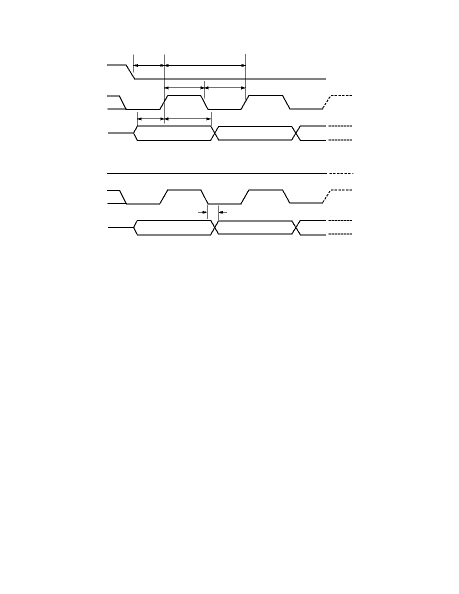
Figure 3a. Serial Register Interface Timing MSB First
CS
SCLK
SDIO
SDO
DATA TRANSFER CYCLE
INSTRUCTION CYCLE
R/W
I6
D7
N
I5
I4
I3
I2
I1
I0
D6
N
D7
N
D6
N
D0
0
D1
0
D2
0
D0
0
D1
0
D2
0
(N)
(N)
Figure 3b. Serial Register Interface Timing LSB First
REV. 0
≠18≠
AD9777
t
DS
t
SCLK
t
PWH
t
PWL
t
DS
t
DH
INSTRUCTION BIT 7
INSTRUCTION BIT 6
CS
SCLK
SDIO
Figure 4. Timing Diagram for Register Write to AD9777
t
DV
DATA BIT N
DATA BIT N≠1
CS
SCLK
SDIO
SDO
Figure 5. Timing Diagram for Register Read from AD9777
NOTES ON SERIAL PORT OPERATION
The AD9777 serial port configuration bits reside in Bits 6 and 7
of Register Address 00h. It is important to note that the configura-
tion changes immediately upon writing to the last bit of the register.
For multibyte transfers, writing to this register may occur during
the middle of the communication cycle. Care must be taken to
compensate for this new configuration for the remaining bytes
of the current communication cycle.
The same considerations apply to setting the reset bit in Register
Address 00h. All other registers are set to their default values, but
the software reset doesn't affect the bits in Register Address 00h.
It is recommended to use only single byte transfers when chang-
ing serial port configurations or initiating a software reset.
A write to Bits 1, 2, and 3 of Address 00h with the same logic
levels as for Bits 7, 6, and 5 (bit pattern: XY1001YX binary) allows
the user to reprogram a lost serial port configuration and to reset
the registers to their default values. A second write to Address
00h with reset bit low and serial port configuration as specified
above (XY) reprograms the OSC IN multiplier setting. A changed
f
SYSCLK
frequency is stable after a maximum of 200 f
MCLK
cycles
(equals wake-up time).
DAC OPERATION
The dual 16-bit DAC output of the AD9777, along with the
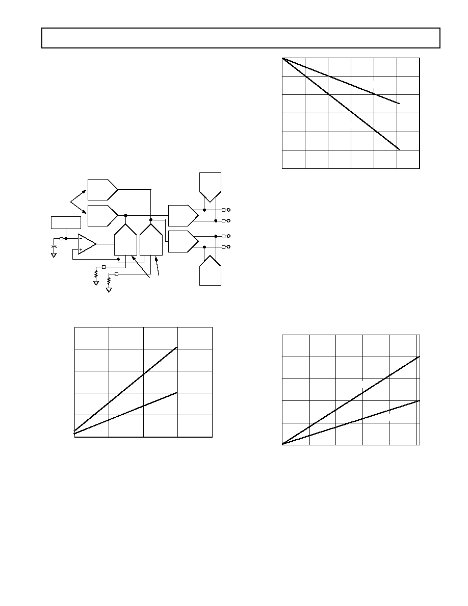
reference circuitry, gain, and offset registers, is shown in Figure 6.
Referring to the transfer functions in Equation 1, a reference
current is set by the internal 1.2 V reference, the external R
SET
resistor, and the values in the coarse gain register. The fine gain
DAC subtracts a small amount from this and the result is input
to IDAC and QDAC, where it is scaled by an amount equal to
1024/24. Figures 7a and 7b show the scaling effect of the coarse
and fine adjust DACs. IDAC and QDAC are PMOS current
source arrays, segmented in a 5-4-7 configuration. The five
most significant bits control an array of 31 current sources. The
next four bits consist of 15 current sources whose values are all
equal to 1/16 of an MSB current source. The seven LSBs are
binary weighted fractions of the middle bit's current sources. All
current sources are switched to either I
OUTA
or I
OUTB
, depend-
ing on the input code.
The fine adjustment of the gain of each channel allows for
improved balance of QAM modulated signals, resulting in
improved modulation accuracy and image rejection. In the
Applications section of this data sheet, performance data is
included that shows to what degree image rejection can be
improved when the AD9777 is used with an AD8345 quadra-
ture modulator from ADI.
REV. 0
AD9777
≠19≠
The offset control defines a small current that can be added
to I
OUTA
or I
OUTB
(not both) on the IDAC and QDAC. The
selection of which I
OUT
this offset current is directed toward is
programmable via Register 08h, Bit 7 (IDAC) and Register 0Ch,
Bit 7 (QDAC). Figure 9 shows the scale of the offset current
that can be added to one of the complementary outputs on the
IDAC and QDAC. Offset control can be used for suppression of
LO leakage resulting from modulation of dc signal components.
If the AD9777 is dc-coupled to an external modulator, this
feature can be used to cancel the output offset on the AD9777
as well as the input offset on the modulator. Figure 9 shows a
typical example of the effect that the offset control has on LO
suppression.
OFFSET
DAC
QDAC
IDAC
OFFSET
DAC
REFIO
0.1 F
FSADJ1
FSADJ2
RSET1
RSET2
I
OUTA1
I
OUTB1
OFFSET
CONTROL
REGISTERS
I
OUTA2
I
OUTB2
GAIN
CONTROL
REGISTERS
COARSE
GAIN
DAC
COARSE
GAIN
DAC
FINE
GAIN
DAC
FINE
GAIN
DAC
1.2VREF
GAIN
CONTROL
REGISTERS
OFFSET
CONTROL
REGISTERS
Figure 6. DAC Outputs, Reference Current Scaling, and
Gain/Offset Adjust
COARSE GAIN REGISTER CODE ≠ Assuming
RSET1, 2 = 1.9k
0
5
COARSE REFERENCE CURRENT ≠ mA
0
25
10
15
20
5
10
15
20
2R MODE
1R MODE
Figure 7a. Coarse Gain Effect on I
FULLSCALE
FINE GAIN REGISTER CODE ≠ Assuming
RSET1, 2 = 1.9k
0
5
FINE REFERENCE CURRENT ≠ mA
≠3.0
10
15
20
2R MODE
1R MODE
≠2.5
≠2.0
≠1.5
≠1.0
≠0.5
0
Figure 7b. Fine Gain Effect on I
FULLSCALE
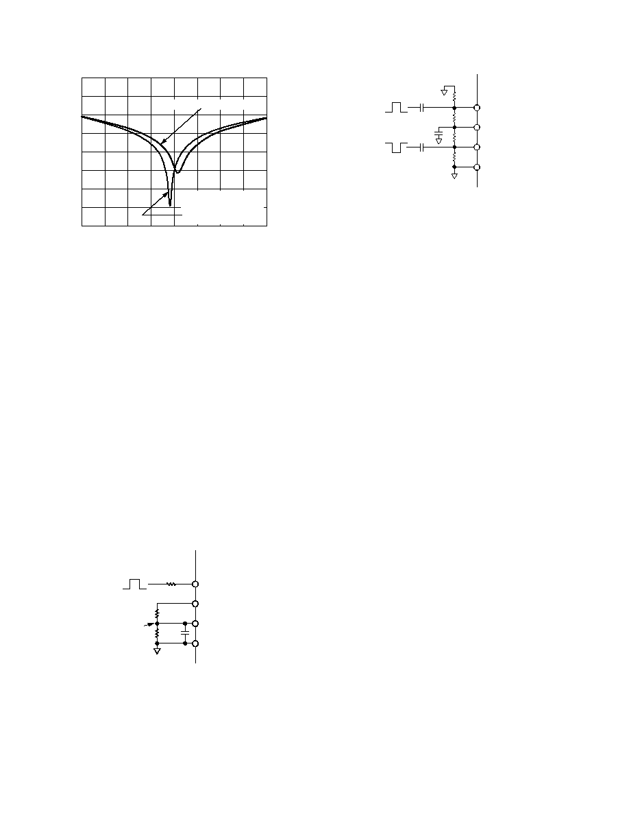
In Figure 9, the negative scale represents an offset added to
I
OUTB
, while the
positive scale represents an offset added to
I
OUTA
of the respective DAC. Offset Register 1 corresponds
to IDAC, while Offset Register 2 corresponds to QDAC. Figure 9
represents the AD9777 synthesizing a complex signal that is
then dc-coupled to an AD8345 quadrature modulator with an
LO of 800 MHz. The dc-coupling allows the input offset of the
AD8345 to be calibrated out as well. The LO suppression at the
AD8345 output was optimized first by adjusting Offset Register 1,
in the AD9777. When an optimal point was found (roughly
Code 54), this code was held in Offset Register 1, and
Offset Register 2 was adjusted. The resulting LO suppression is
70 dBFS. These are typical numbers, and the specific code for
optimization will vary from part to part.
COARSE GAIN REGISTER CODE ≠ Assuming
RSET1, 2 = 1.9k
0
200
OFFSET CURRENT ≠ mA
0
5
400
600
800
1
2
3
4
2R MODE
1R MODE
1000
Figure 8. DAC Output Offset Current
REV. 0
≠20≠
AD9777
OFFSET REGISTER 1 ADJUSTED
DAC1, DAC2 ≠ Offset Register Codes
≠1024
≠768
LO SUPPRESSION ≠ dBFS
≠80
0
1024
≠512
≠256
0
256
512
768
≠70
≠60
≠50
≠40
≠30
≠20
≠10
OFFSET REGISTER 2
ADJUSTED, WITH OFFSET
REGISTER 1 SET
TO OPTIMIZED VALUE
Figure 9. Offset Adjust Control, Effect on LO Suppression
1R/2R MODE
In the 2R mode, the reference current for each channel is set
independently by the FSADJ resistor on that channel. The
AD9777 can be programmed to derive its reference current from a
single resistor on Pin 60 by placing the part in the 1R mode. The
transfer functions in Equation 1 are valid for the 2R mode. In the
1R mode, the current developed in the single FSADJ resistor is
split equally between the two channels. The result is that in the
1R mode, a scale factor of one-half must be applied to the formulas
in Equation 1. The full-scale DAC current in the 1R mode can still
be set to as high as 20 mA by using the internal 1.2 V reference and
a 950
resistor, instead of the 1.9 k resistor typically used
in the 2R mode.
CLOCK INPUT CONFIGURATIONS
The clock inputs to the AD9777 can be driven differentially or
single-ended. The internal clock circuitry has supply and ground
(CLKVDD, CLKGND) separate from the other supplies on the
chip to minimize jitter from internal noise sources.
Figure 10 shows the AD9777 driven from a single-ended clock
source. The CLK+/CLK≠ Pins form a differential input (CLKIN),
so that the statically terminated input must be dc-biased to the
midswing voltage level of the clock driven input.
R
SERIES
V
THRESHOLD
AD9777
CLK+
CLKVDD
CLK≠
CLKGND
0.1 F
Figure 10. Single-Ended Clock Driving Clock
Inputs
A configuration for differentially driving the clock inputs is
given in Figure 11. DC-blocking capacitors can be used to
couple a clock driver output whose voltage swings exceed
CLKVDD or CLKGND. If the driver voltage swings are within
the supply range of the AD9777, the dc-blocking capacitors
and bias resistors are not necessary.
AD9777
CLK+
CLKVDD
CLK≠
CLKGND
0.1 F
1k
ECL/PECL
1k
1k
1k
0.1 F
0.1 F
Figure 11. Differential Clock Driving Clock Inputs
A transformer, such as the T1-1T from Mini-Circuits, can also be
used to convert a single-ended clock to differential. This method is
used on the AD9777 evaluation board so that an external sine
wave with no dc offset can be used as a differential clock.
PECL/ECL drivers require varying termination networks, the
details of which are left out of Figures 10 and 11 but can be found
in application notes such as AND8020/D from On Semiconductor.
These networks depend on the assumed transmission line imped-
ance and power supply voltage of the clock driver. Optimum
performance of the AD9777 is achieved when the driver is placed
very close to the AD9777 clock inputs, thereby negating any
transmission line effects such as reflections due to mismatch.
The quality of the clock and data input signals is important in
achieving optimum performance. The external clock driver cir-
cuitry should provide the AD9777 with a low jitter clock input
that meets the min/max logic levels while providing fast edges.
Although fast clock edges help minimize any jitter that will manifest
itself as phase noise on a reconstructed waveform, the high gain
bandwidth product of the AD9777's differential comparator can
tolerate sine wave inputs as low as 0.5 V p-p, with minimal
degradation of the output noise floor.
PROGRAMMABLE PLL
CLKIN can function either as an input data rate clock (PLL
enabled) or as a DAC data rate clock (PLL disabled) according
to the state of Address 02h, Bit 7 in the SPI port register. The
internal operation of the AD9777 clock circuitry in these two
modes is illustrated in Figures 12 and 13.
The PLL clock multiplier and distribution circuitry produce the
necessary internal synchronized 1
◊, 2◊, 4◊, and 8◊ clocks for the
rising edge triggered latches, interpolation filters, modulators, and
DACs. This circuitry consists of a phase detector, charge pump,
voltage controlled oscillator (VCO), prescaler, clock distribution,
and SPI port control. The charge pump and VCO are powered
from PLLVDD while the differential clock input buffer, phase
detector, prescaler, and clock distribution are powered from
CLKVDD. PLL lock status is indicated by the logic signal at the
PLL_LOCK Pin, as well as by the status of Bit 1, Register 00h.
To ensure optimum phase noise performance from the PLL clock
multiplier, and distribution, PLLVDD and CLKVDD should
originate from the same clean analog supply. The speed of the
VCO with the PLL enabled also has an effect on phase noise.
Optimal phase noise with respect to VCO speed is achieved by
running the VCO in the range of 450 MHz to 550 MHz. The
VCO speed is a function of the input data rate, the interpolation
rate, and the VCO prescaler, according to the following function:
VCO Speed MHz
Input Data Rate MHz
InterpolationRate
escaler
(
)
(
)
=
◊
◊ Pr
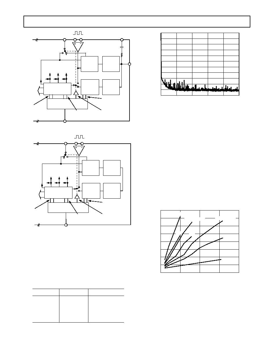
REV. 0
AD9777
≠21≠
CHARGE
PUMP
PHASE
DETECTOR
CLK+
CLOCK
DISTRIBUTION
CIRCUITRY
VCO
AD9777
CLK≠
SPI PORT
INTERNAL SPI
CONTROL
REGISTERS
PLL_LOCK
1 = LOCK
0 = NO LOCK
PLLVDD
LPF
INTERPOLATION
FILTERS,
MODULATORS,
AND DACS
2
8
INTERPOLATION
RATE
CONTROL
PLL DIVIDER
(PRESCALER)
CONTROL
PLL
CONTROL
(PLL ON)
1
INPUT
DATA
LATCHES
MODULATION
RATE
CONTROL
PRESCALER
4
Figure 12. PLL and Clock Circuitry with PLL Enabled
CHARGE
PUMP
PHASE
DETECTOR
CLK+
CLOCK
DISTRIBUTION
CIRCUITRY
VCO
AD9777
CLK≠
SPI PORT
INTERNAL SPI
CONTROL
REGISTERS
PLL_LOCK
1 = LOCK
0 = NO LOCK
INTERPOLATION
FILTERS,
MODULATORS,
AND DACS
2
8
INTERPOLATION
RATE
CONTROL
PLL DIVIDER
(PRESCALER)
CONTROL
PLL
CONTROL
(PLL ON)
1
INPUT
DATA
LATCHES
MODULATION
RATE
CONTROL
PRESCALER
4
Figure 13. PLL and Clock Circuitry with PLL Disabled
In addition, if the zero stuffing option is enabled, the VCO will
double its speed again. Phase noise may be slightly higher with
the PLL enabled. Figure 14 illustrates typical phase noise per-
formance of the AD9777 with 2
◊ interpolation and various
input data rates. The signal synthesized for the phase noise
measurement was a single carrier at a frequency of f
DATA
/4.
The repetitive nature of this signal eliminated quantization noise
and distortion spurs as a factor in the measurement. Although
the curves blend together in Figure 14, the different conditions
are called out here for clarity.
f
DATA
PLL
Prescaler Ratio
125 MSPS
Disabled
125 MSPS
Enabled
div1
100 MSPS
Enabled
div2
75 MSPS
Enabled
div2
50 MSPS
Enabled
div4
FREQUENCY OFFSET ≠ MHz
PHASE NOISE ≠ dBFS ≠80
0
0
≠70
≠60
≠50
≠40
≠30
≠20
≠10
≠90
≠110
≠100
1
2
3
4
5
Figure 14. Phase Noise Performance
It is important to note that the resistor/capacitor needed for the
PLL loop filter is internal on the AD9777. This will suffice unless
the input data rate is below 10 MHz, in which case an external
series RC is required between the LPF and PLLVDD Pins.
POWER DISSIPATION
The AD9777 has three voltage supplies: AVDD, DVDD, and
CLKVDD. Figures 15, 16, and 17 show the current required
from each of these supplies when each is set to the 3.3 V nomi-
nal specified for the AD9777. Power dissipation (P
D
) can easily
be extracted by multiplying the given curves by 3.3. As Figure 15
shows, I
DVDD
is very dependent on the input data rate, the
interpolation rate, and the activation of the internal digital
modulator. I
DVDD
, however, is relatively insensitive to the
modulation rate by itself. In Figure 16, I
AVDD
shows the same
type of sensitivity to data, interpolation rate, and the modulator
function but to a much lesser degree (<10%). In Figure 17,
I
CLKVDD
varies over a wide range yet is responsible for only a small
percentage of the overall AD9777 supply current requirements.
f
DATA
≠ MHz
0
50
I
DVDD
≠ mA
0
100
150
200
50
100
150
200
250
300
350
400
8
(MOD. ON)
,
4
(MOD. ON)
,
2
(MOD. ON)
,
8
4
2
1
Figure 15. I
DVDD
vs. f
DATA
vs. Interpolation Rate,
PLL Disabled
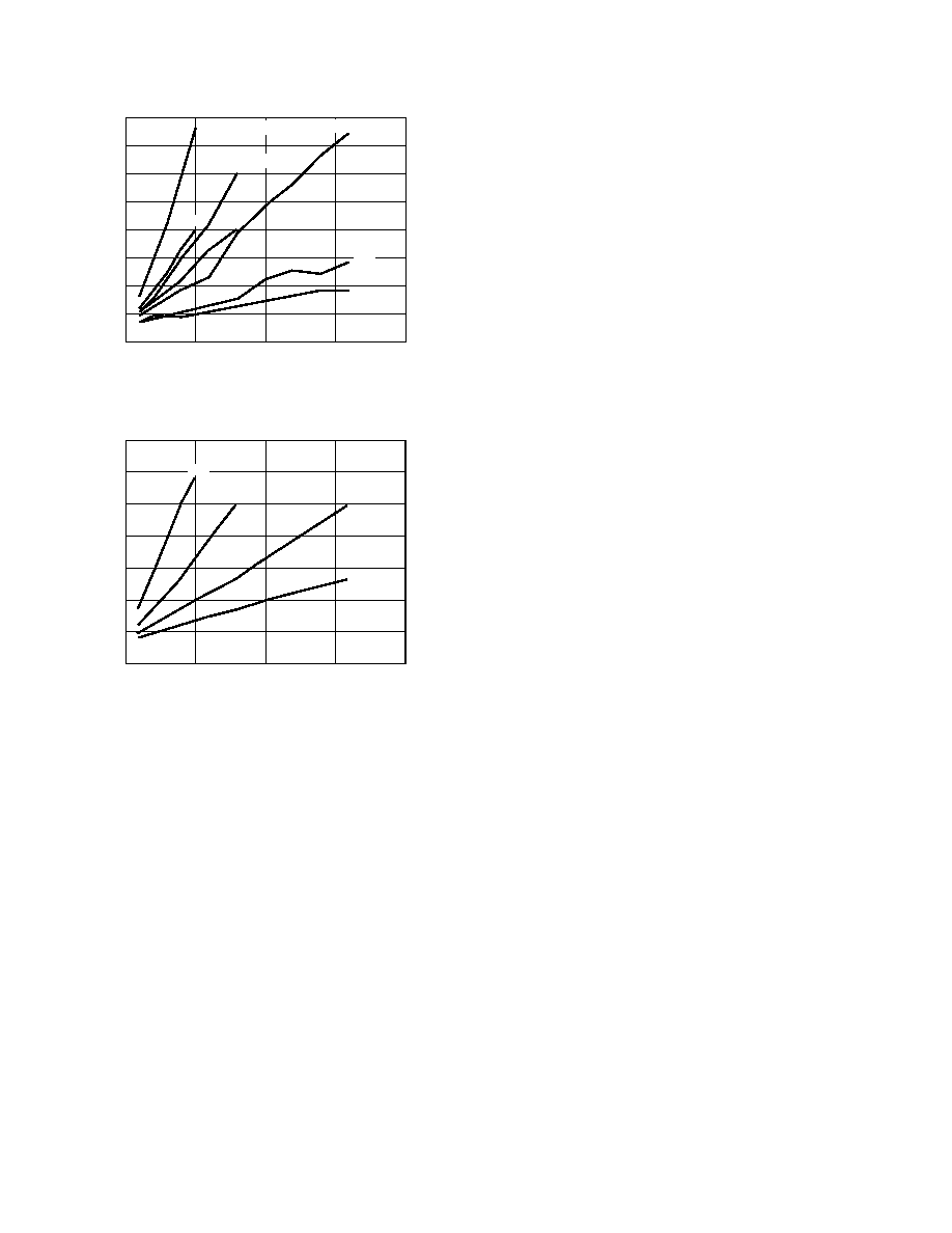
REV. 0
≠22≠
AD9777
f
DATA
≠ MHz
0
50
I
AVDD
≠ mA
72.0
100
150
200
72.5
8
(MOD. ON)
,
4
(MOD. ON)
,
2
(MOD. ON)
,
8
4
2
1
73.0
73.5
74.0
74.5
75.0
75.5
76.0
Figure 16. I
AVDD
vs. f
DATA
vs. Interpolation Rate,
PLL Disabled
f
DATA
≠ MHz
0
50
I
CLKVDD
≠ mA
0
100
150
200
5
10
15
20
25
30
35
8
4
2
1
Figure 17. I
CLKVDD
vs. f
DATA
vs. Interpolation Rate,
PLL Disabled
SLEEP/POWER-DOWN MODES
(Control Register 00h, Bits 3 and 4)
The AD9777 provides two methods for programmable reduction
in power savings. The sleep mode, when activated, turns off the
DAC output currents but the rest of the chip remains functioning.
When coming out of sleep mode, the AD9777 will immediately
return to full operation. Power-down mode, on the other hand,
turns off all analog and digital circuitry in the AD9777 except
for the SPI port. When returning from power-down mode, enough
clock cycles must be allowed to flush the digital filters of random
data acquired during the power-down cycle. Note that optimal
performance with the PLL enabled is achieved with the UCO in
the PLL control loop running at 450 MHz ≠ 550 MHz.
ONE/TWO PORT INPUT MODES
The digital data input ports can be configured as two independent
ports or as a single (one port mode) port. In two port mode, the
AD9777 can be programmed to generate an externally available
data rate clock (DATACLK) for the purpose of data synchroniza-
tion. Data at the two input ports can be latched into the AD9777
on every rising clock edge of DATACLK. In one port mode,
P2B14 and P2B15 from input data Port 2 are redefined as IQSEL
and ONEPORTCLK, respectively. The input data in one port
mode is steered to one of the two internal data channels based on
the logic level of IQSEL. A clock signal, ONEPORTCLK, is
generated by the AD9777 in this mode for the purpose of external
data synchronization. ONEPORTCLK runs at the input inter-
leaved data rate, which is 2
◊ the data rate at the internal input
to either channel.
Test configurations showing the various clocks that are required and
produced by the AD9777 in the PLL and one/two port modes are
given in Figures 55 through 58. Jumper positions needed to oper-
ate the AD9777 evaluation board in these modes are given as well.
PLL ENABLED, TWO PORT MODE
(Control Register 02h, Bits 6≠0 and 04h, Bits 7≠1)
With the phase-locked loop (PLL) enabled and the AD9777 in
two port mode, the speed of CLKIN is inherently that of the input
data rate. In two port mode, Pin 8 (DATACLK/PLL_ LOCK)
can be programmed (Control Register 01h, Bit 0) to function as
either a lock indicator for the internal PLL or as a clock running
at the input data rate. When Pin 8 is used as a clock output
(DATACLK), its frequency is equal to that of CLKIN. Data at
the input ports is latched into the AD9777 on the rising edge of the
CLKIN. Figure 18 shows the delay, t
OD
, inherent between the
rising edge of CLKIN and the rising edge of DATACLK, as well
as the setup and hold requirements for the data at Ports 1 and 2.
Note that the setup and hold times given in Figure 18 are the
input data transitions with respect to CLKIN. t
OD
can vary with
CLKIN speed, PLL divider setting, and interpolation rate. It is
therefore highly recommended that the input data be synchro-
nized to CLKIN rather than DATACLK when the PLL is enabled.
Note that in two port mode (PLL enabled or disabled), the data
rate at the interpolation filter inputs is the same as the input data
rate at Ports 1 and 2.
The DAC output sample rate in two port mode is equal to the
clock input rate multiplied by the interpolation rate. If zero
stuffing is used, another factor of two must be included to cal-
culate the DAC sample rate.
DATACLK Inversion
(Control Register 02h, Bit 4)
By programming this bit, the DATACLK signal shown in
Figure 18 can be inverted. With inversion enabled, t
OD
will
refer to the time between the rising edge of CLKIN and the
falling edge of DATACLK. No other effect on timing will occur.
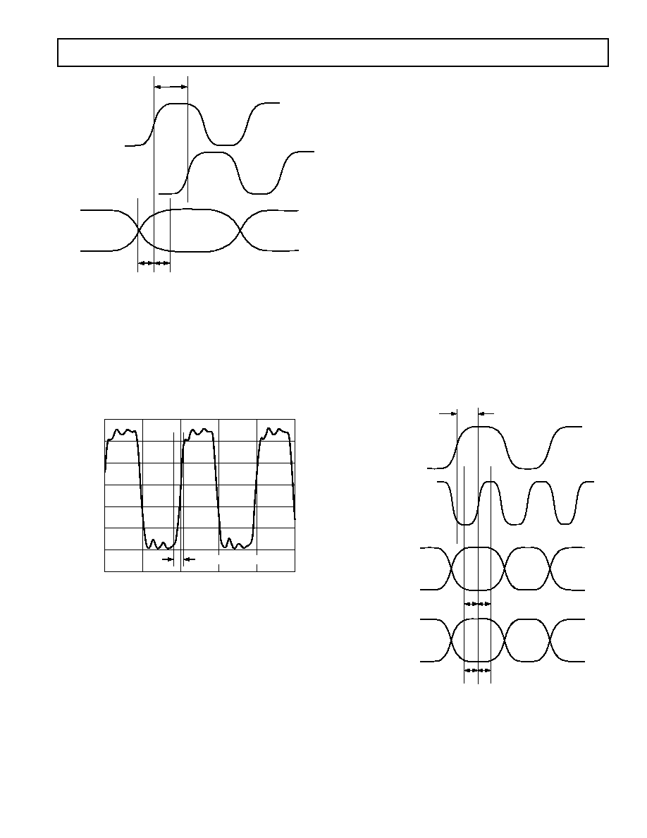
REV. 0
AD9777
≠23≠
CLKIN
DATACLK
DATA AT PORTS
1 AND 2
t
OD
t
H
t
S
t
S
= 0.0ns
t
H
= 2.5ns
(TYP SPECS)
Figure 18. Timing Requirements in Two Port
Input Mode with PLL Enabled
DATACLK DRIVER STRENGTH
(Control Register 02h, Bit 5)
The DATACLK output driver strength is capable of driving
>10 mA into a 330
load while providing a rise time of 3 ns.
Figure 19 shows DATACLK driving a 330
resistive load at a
frequency of 50 MHz. By enabling the drive strength option
(Control Register 02h, Bit 5), the amplitude of DATACLK
under these conditions will be increased by approximately 200 mV.
TIME ≠ ns
0
10
FREQUENCY ≠ V
≠0.5
20
30
40
0
0.5
1.0
1.5
2.0
2.5
3.0
50
DELTA APPROX. 2.8ns
Figure 19. DATACLK Driver Capability into 330
at 50 MHz
PLL ENABLED, ONE PORT MODE
(Control Register 02h, Bits 6≠1 and 04h, Bits 7≠1)
In one port mode, the I and Q channels receive their data from an
interleaved stream at digital input Port 1. The function of Pin 32
is defined as an output (ONEPORTCLK) that generates a clock at
the interleaved data rate, which is 2 the internal input data rate
of the I and Q channels. The frequency of CLKIN is equal to the
internal input data rate of the I and Q channels. The selection of
the data for the I or Q channel is determined by the state of the logic
level at Pin 31 (IQSEL when the AD9777 is in one port mode)
on the rising edge of ONEPORTCLK. IQSEL = 1 under these
conditions will latch the data into the I channel on the clock rising
edge, while IQSEL = 0 will latch the data into the Q channel.
It is possible to invert the I and Q selection by setting Control
Register 02h, Bit 1 to the invert state (Logic "1"). Figure 20
illustrates the timing requirements for the data inputs as well as
the IQSEL input. Note that the 1
◊ interpolation rate is not
available in one port mode.
The DAC output sample rate in one port mode is equal to
CLKIN multiplied by the interpolation rate. If zero stuffing is
used, another factor of 2 must be included to calculate the
DAC sample rate.
ONEPORTCLK INVERSION
(Control Register 02h, Bit 2)
By programming this bit, the ONEPORTCLK signal shown in
Figure 20 can be inverted. With inversion enabled, t
OD
refers to
the delay between the rising edge of the external clock and the
falling edge of ONEPORTCLK. The setup and hold times, t
S
and
t
H
,
will be with respect to the falling edge of ONEPORTCLK.
There will be no other effect on timing.
ONEPORTCLK DRIVER STRENGTH
The drive capability of ONEPORTCLK is identical to that of
DATACLK in the two port mode. Refer to Figure 19 for per-
formance under load conditions.
t
OD
t
H
t
S
CLKIN
I AND Q INTERLEAVED
INPUT DATA AT PORT 1
ONEPORTCLK
IQSEL
t
IQH
t
IQS
t
OD
= 4.7ns
t
S
= 3.0ns
t
H
= ≠0.5ns
t
IQS
= 3.5ns
t
IQH
= ≠1.5ns
Figure 20. Timing Requirements in One Port
Input Mode, with the PLL Enabled
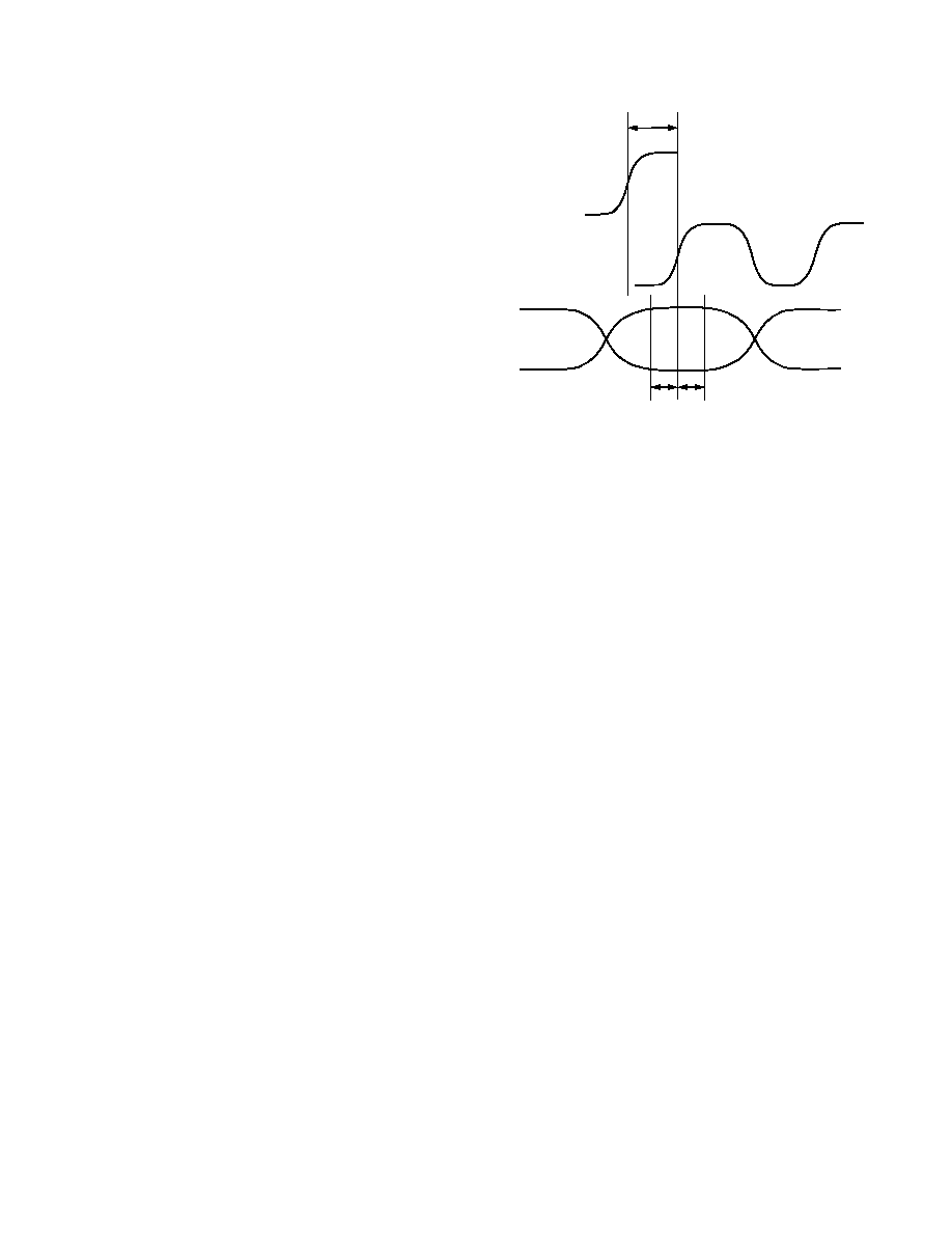
REV. 0
≠24≠
AD9777
IQ PAIRING
(Control Register 02h, Bit 0)
In one port mode, the interleaved data is latched into the AD9777
internal I and Q channels in pairs. The order of how the pairs
are latched internally is defined by this control register. The
following is an example of the effect this has on incoming inter-
leaved data.
Given the following interleaved data stream, where the data
indicates the value with respect to full scale:
I
Q
I
Q
I
Q
I
Q
I
Q
0.5
0.5
1
1
0.5
0.5
0
0
0.5
0.5
With the control register set to "0" (I first), the data will appear
at the internal channel inputs in the following order in time:
I channel
0.5
1
0.5
0
0.5
Q channel
0.5
1
0.5
0
0.5
With the control register set to "1" (Q first), the data will appear at
the internal channel inputs in the following order in time:
I channel
0.5
1
0.5
0
0.5
x
Q channel
y
0.5
1
0.5
0
0.5
The values x and y represent the next I value and the previous
Q value in the series.
PLL DISABLED, TWO PORT MODE
With the PLL disabled, a clock at the DAC output rate must be
applied to CLKIN. Internal clock dividers in the AD9777 syn-
thesize the DATACLK signal at Pin 8, which runs at the input
data rate and can be used to synchronize the input data. Data is
latched into input Ports 1 and 2 of the AD9777 on the rising
edge of DATACLK. DATACLK speed is defined as the speed
of CLKIN divided by the interpolation rate. With zero stuffing
enabled, this division increases by a factor of 2. Figure 21
illustrates the delay between the rising edge of CLKIN and
the rising edge of DATACLK, as well as t
S
and
t
H
in this mode.
The programmable modes DATACLK inversion and DATACLK
driver strength described in the previous section (PLL Enabled,
Two Port Mode) have identical functionality with the PLL disabled.
As described earlier in the PLL-Enabled Mode section, t
OD
can
vary depending on CLKIN frequency and interpolation rate.
However, with the PLL disabled, the input data latches are closely
synchronized to DATACLK so that it is recommended in this
mode that the input data be timed from DATACLK, not CLKIN.
CLKIN
DATACLK
DATA AT PORTS
1 AND 2
t
OD
t
H
t
S
t
S
= 5.0ns
t
H
= ≠3.2ns
(TYP SPECS)
Figure 21. Timing Requirements in Two Port
Input Mode, with PLL Disabled
PLL DISABLED, ONE PORT MODE
In one port mode, data is received into the AD9777 as an
interleaved stream on Port 1. A clock signal (ONEPORTCLK),
running at the interleaved data rate, which is 2
◊ the input data
rate of the internal I and Q channels is available for data syn-
chronization at Pin 32.
With PLL disabled, a clock at the DAC output rate must be applied
to CLKIN. Internal dividers synthesize the ONEPORTCLK
signal at Pin 32. The selection of the data for the I or Q channel
is determined by the state of the logic level applied to Pin 31
(IQSEL when the AD9777 is in one port mode) on the rising
edge of ONEPORTCLK. IQSEL = 1 under these conditions
will latch the data into the I channel on the clock rising edge,
while IQSEL = 0 will latch the data into the Q channel. It is
possible to invert the I and Q selection by setting Control
Register 02h, Bit 1 to the invert state (Logic "1"). Figure 22
illustrates the timing requirements for the data inputs as well as
the IQSEL input. Note that the 1
◊ interpolation rate is not
available in the one port mode.
One port mode is very useful when interfacing with devices
such as Analog Devices' AD6622 or AD6623 transmit signal
processors, in which two digital data channels have been
interleaved (multiplexed).
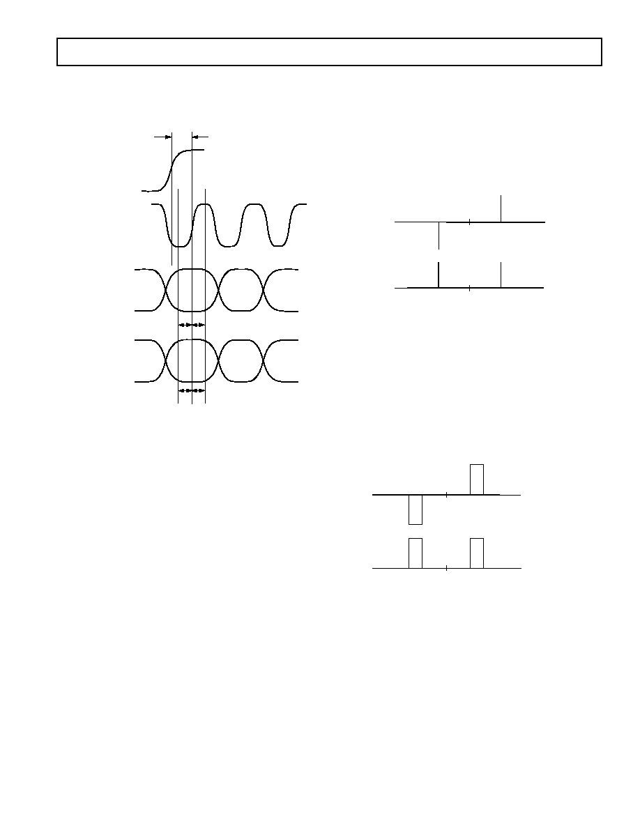
REV. 0
AD9777
≠25≠
The programmable modes' ONEPORTCLK inversion,
ONEPORTCLK driver strength, and IQ pairing described in
the previous section (PLL Enabled, One Port Mode) have
identical functionality with the PLL disabled.
t
OD
t
H
t
S
CLKIN
I AND Q INTERLEAVED
INPUT DATA AT PORT 1
ONEPORTCLK
IQSEL
t
IQH
t
IQS
t
OD
= 4.7ns
t
S
= 3.0ns
t
H
= ≠1.0ns
t
IQS
= 3.5ns
t
IQH
= ≠1.5ns
(TYP SPECS)
Figure 22. Timing Requirements in One Port
Input Mode, with PLL Disabled
DIGITAL FILTER MODES
The I and Q data paths of the AD9777 have their own indepen-
dent half-band FIR filters. Each data path consists of three FIR
filters, providing up to 8
◊ interpolation for each channel. The rate
of interpolation is determined by the state of Control Register 01h,
Bits 7 and 6. Figures 1a≠1c show the response of the digital
filters when the AD9777 is set to 2
◊, 4◊, and 8◊ modes. The
frequency axes of these graphs have been normalized to the input
data rate of the DAC. As the graphs show, the digital filters can
provide greater than 75 dB of out-of-band rejection.
An online tool is available for quick and easy analysis of the
AD9777 interpolation filters in the various modes. The link
can be accessed at:
www.analog.com/techSupport/designTools/
interactiveTools/dac/ad9777image.html
.
AMPLITUDE MODULATION
Given two sine waves at the same frequency, but with a 90 phase
difference, a point of view in time can be taken such that the
waveform that leads in phase is cosinusoidal and the waveform
that lags is sinusoidal. Analysis of complex variables states that
the cosine waveform can be defined as having real positive and
negative frequency components, while the sine waveform consists
of imaginary positive and negative frequency images. This is
shown graphically in the frequency domain in Figure 23.
DC
DC
e
≠j t
/2j
COSINE
SINE
e
≠j t
/2
e
≠j t
/2j
e
≠j t
/2
Figure 23. Real and Imaginary Components of
Sinusoidal and Cosinusoidal Waveforms
Amplitude modulating a baseband signal with a sine or a cosine
convolves the baseband signal with the modulating carrier in
the frequency domain. Amplitude scaling of the modulated
signal reduces the positive and negative frequency images by a
factor of two. This scaling will be very important in the discus-
sion of the various modulation modes. The phase relationship of
the modulated signals is dependent on whether the modulating
carrier is sinusoidal or cosinusoidal, again with respect to the
reference point of the viewer. Examples of sine and cosine
modulation are given in Figure 24.
SINUSOIDAL
MODULATION
DC
DC
Ae
≠j t
/2j
Ae
≠j t
/2
Ae
≠j t
/2
Ae
≠j t
/2j
COSINUSOIDAL
MODULATION
Figure 24. Baseband Signal, Amplitude
Modulated with Sine and Cosine Carriers
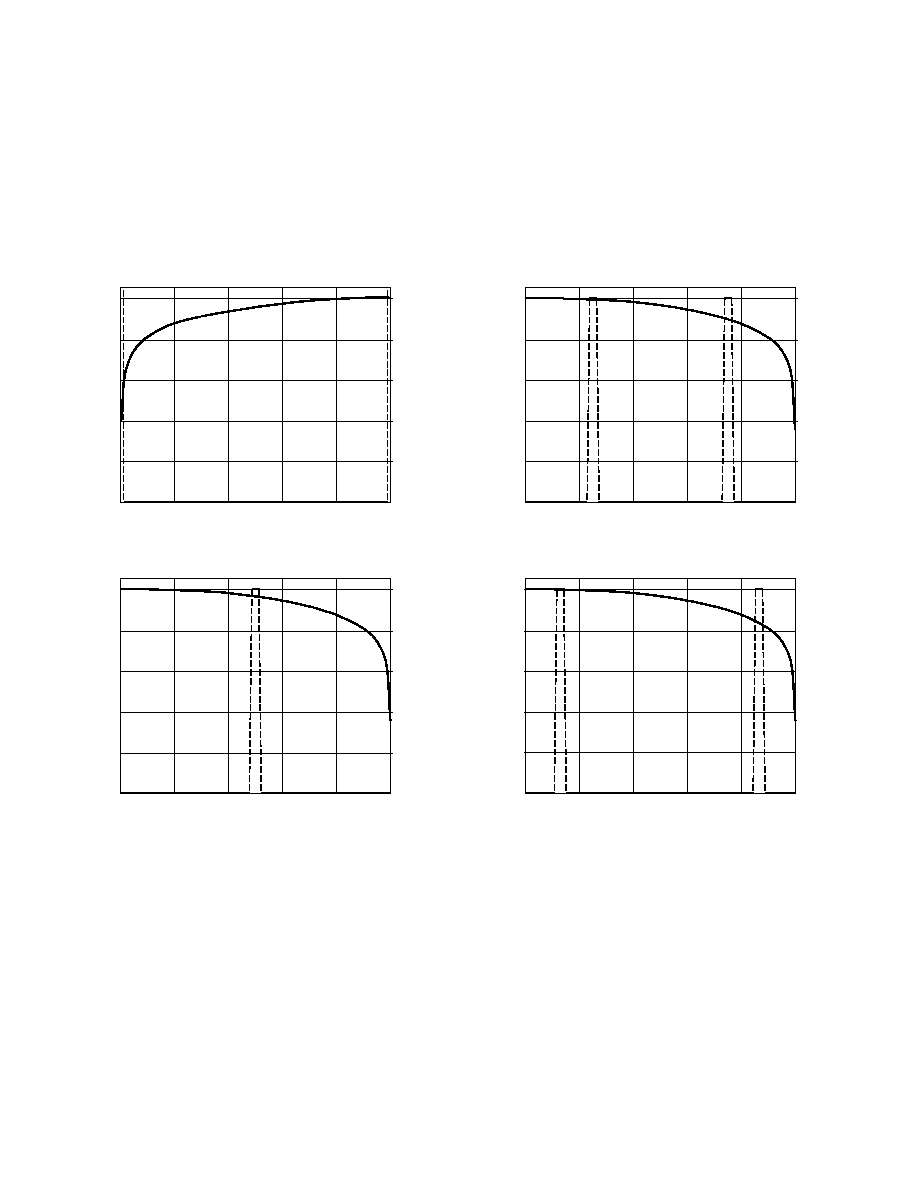
REV. 0
≠26≠
AD9777
MODULATION, NO INTERPOLATION
With Control Register 01h, Bits 7 and 6 set to "00," the inter-
polation function on the AD9777 is disabled. Figures 25a≠25d
show the DAC output spectral characteristics of the AD9777 in
the various modulation modes, all with the interpolation filters
disabled. The modulation frequency is determined by the state
of Control Register 01h, Bits 5 and 4. The tall rectangles
represent the digital domain spectrum of a baseband signal of
narrow bandwidth. By comparing the digital domain spectrum
to the DAC SIN(x)/x roll-off, an estimate can be made for the
characteristics required for the DAC reconstruction filter. Note
also, per the previous discussion on amplitude modulation, that
the spectral components (where modulation is set to f
S
/4 or f
S
/8)
are scaled by a factor of 2. In the situation where the modula-
tion is f
S
/2, the modulated spectral components add constructively
and there is no scaling effect.
f
OUT
(
f
DATA
)
0
0.2
AMPLITUDE ≠ dBFS
≠100
0
≠80
≠60
≠40
≠20
0.4
0.6
0.8
1.0
Figure 25a. No Interpolation, Modulation Disabled
f
OUT
(
f
DATA
)
0
0.2
AMPLITUDE ≠ dBFS
≠100
0
≠80
≠60
≠40
≠20
0.4
0.6
0.8
1.0
Figure 25b. No Interpolation, Modulation = f
DAC
/2
f
OUT
(
f
DATA
)
0
0.2
AMPLITUDE ≠ dBFS
≠100
0
≠80
≠60
≠40
≠20
0.4
0.6
0.8
1.0
Figure 25c. No Interpolation, Modulation = f
DAC
/4
f
OUT
(
f
DATA
)
0
0.2
AMPLITUDE ≠ dBFS
≠100
0
≠80
≠60
≠40
≠20
0.4
0.6
0.8
1.0
Figure 25d. No Interpolation, Modulation = f
DAC
/8
Figure 25. Effects of Digital Modulation on DAC Output Spectrum, Interpolation Disabled
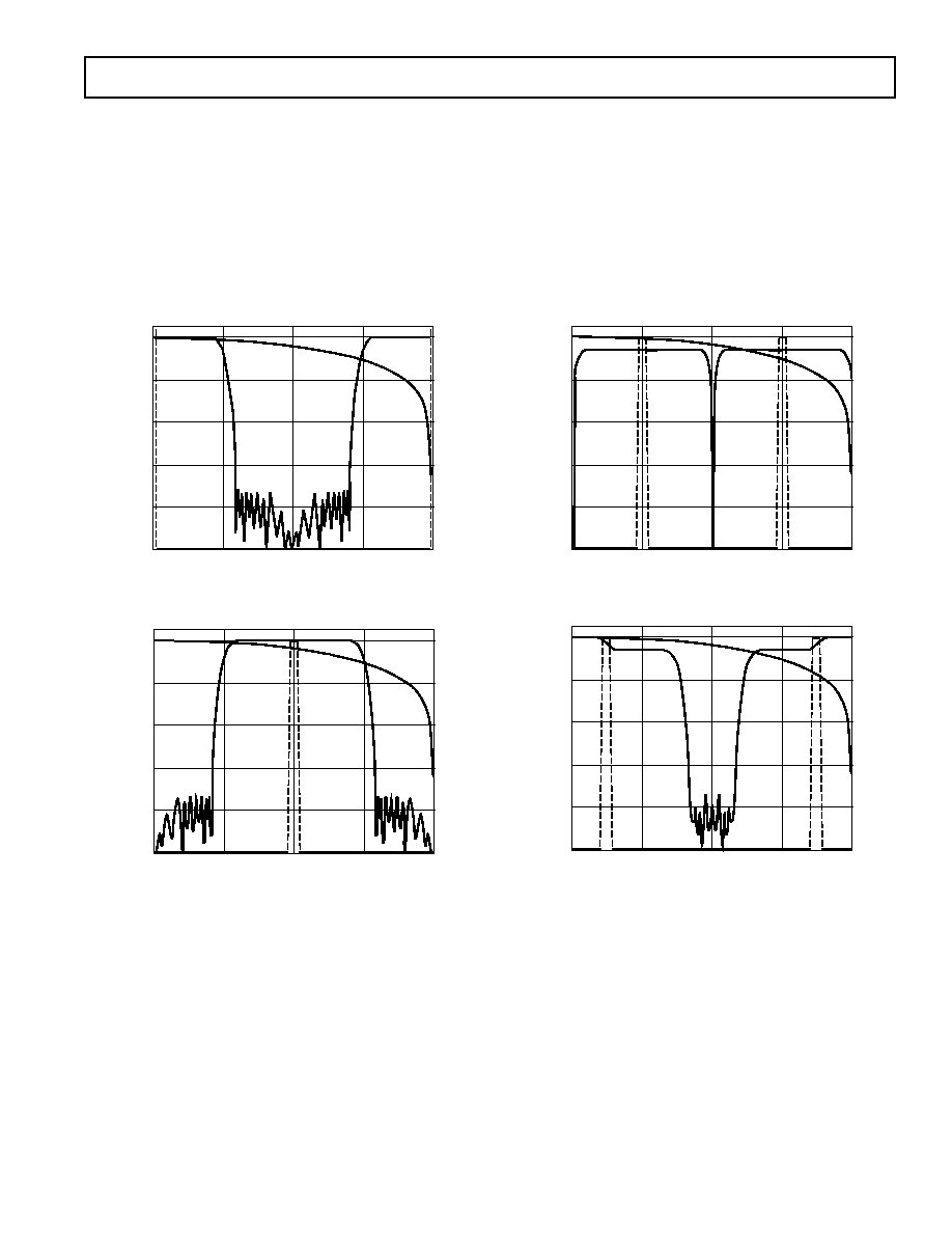
REV. 0
AD9777
≠27≠
MODULATION, INTERPOLATION = 2
◊
With Control Register 01h, Bits 7 and 6 set to "01," the inter-
polation rate of the AD9777 is 2
◊. Modulation is achieved by
multiplying successive samples at the interpolation filter output
by the sequence (1, ≠1). Figures 26a≠26d represent the spectral
response of the AD9777 DAC output with 2
◊ interpolation in the
various modulation modes to a narrow band baseband signal (again,
the tall rectangles in the graphic). The advantage of interpolation
becomes clear in Figures 26a≠26d, where it can be seen that the
images that would normally appear in the spectrum around the
input data rate frequency are suppressed by >70 dB. Another
significant point is that the interpolation filtering is done previous
to the digital modulator. For this reason, as Figures 26a≠26d
show, the pass band of the interpolation filters can be frequency
shifted, giving the equivalent of a high-pass digital filter.
Note that when using the f
S
/4 modulation mode, there is no true
stop band as the band edges coincide with each other. In the f
S
/8
modulation mode, amplitude scaling occurs over only a portion of
the digital filter pass band due to constructive addition over just
that section of the band.
Figure 26. Effects of Digital Modulation on DAC Output Spectrum, Interpolation = 2
◊
f
OUT
(
f
DATA
)
0
0.5
AMPLITUDE ≠ dBFS
≠100
0
≠80
≠60
≠40
≠20
1.0
1.5
2.0
Figure 26a. 2
◊ Interpolation, Modulation = Disabled
f
OUT
(
f
DATA
)
0
0.5
AMPLITUDE ≠ dBFS
≠100
0
≠80
≠60
≠40
≠20
1.0
1.5
2.0
Figure 26b. 2
◊ Interpolation, Modulation = f
DAC
/2
f
OUT
(
f
DATA
)
0
0.5
AMPLITUDE ≠ dBFS
≠100
0
≠80
≠60
≠40
≠20
1.0
1.5
2.0
Figure 26c. 2
◊ Interpolation, Modulation = f
DAC
/4
f
OUT
(
f
DATA
)
0
0.5
AMPLITUDE ≠ dBFS
≠100
0
≠80
≠60
≠40
≠20
1.0
1.5
2.0
Figure 26d. 2
◊ Interpolation, Modulation = f
DAC
/8
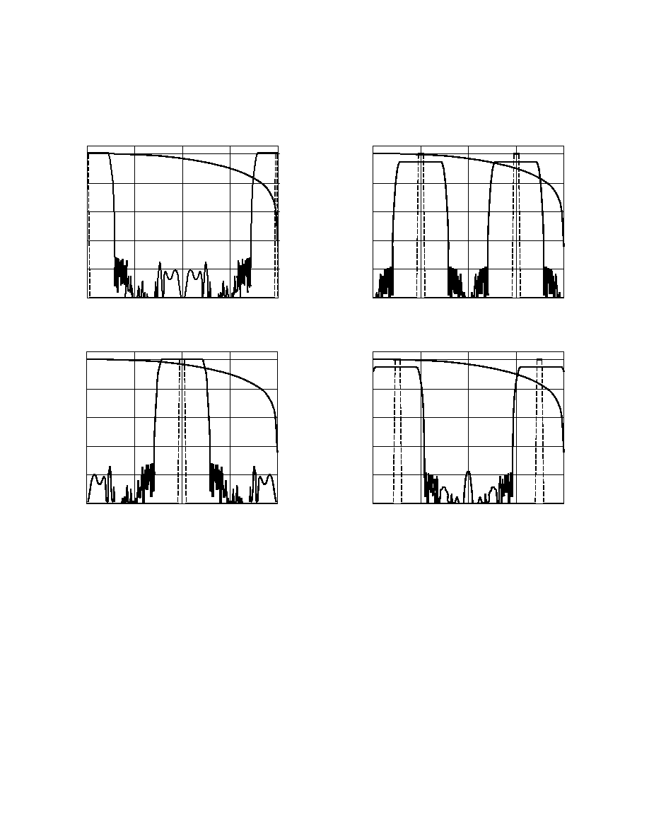
REV. 0
≠28≠
AD9777
f
OUT
(
f
DATA
)
0
1
AMPLITUDE ≠ dBFS
≠100
0
≠80
≠60
≠40
≠20
2
3
4
Figure 27a. 4
◊ Interpolation, Modulation Disabled
f
OUT
(
f
DATA
)
0
1
AMPLITUDE ≠ dBFS
≠100
0
≠80
≠60
≠40
≠20
2
3
4
Figure 27b. 4
◊ Interpolation, Modulation = f
DAC
/2
f
OUT
(
f
DATA
)
0
1
AMPLITUDE ≠ dBFS
≠100
0
≠80
≠60
≠40
≠20
2
3
4
Figure 27c. 4
◊ Interpolation, Modulation = f
DAC
/4
f
OUT
(
f
DATA
)
0
1
AMPLITUDE ≠ dBFS
≠100
0
≠80
≠60
≠40
≠20
2
3
4
Figure 27d. 4
◊ Interpolation, Modulation = f
DAC
/8
Figure 27. Effect of Digital Modulation on DAC Output Spectrum, Interpolation = 4
◊
MODULATION, INTERPOLATION = 4
◊
With Control Register 01h, Bits 7 and 6 set to "10," the inter-
polation rate of the AD9777 is 4
◊. Modulation is achieved by
multiplying successive samples at the interpolation filter output
by the sequence (0, 1, 0, ≠1). Figures 27a≠27d represent the
spectral response of the AD9777 DAC output with 4
◊ interpo-
lation in the various modulation modes to a narrow band
baseband signal.
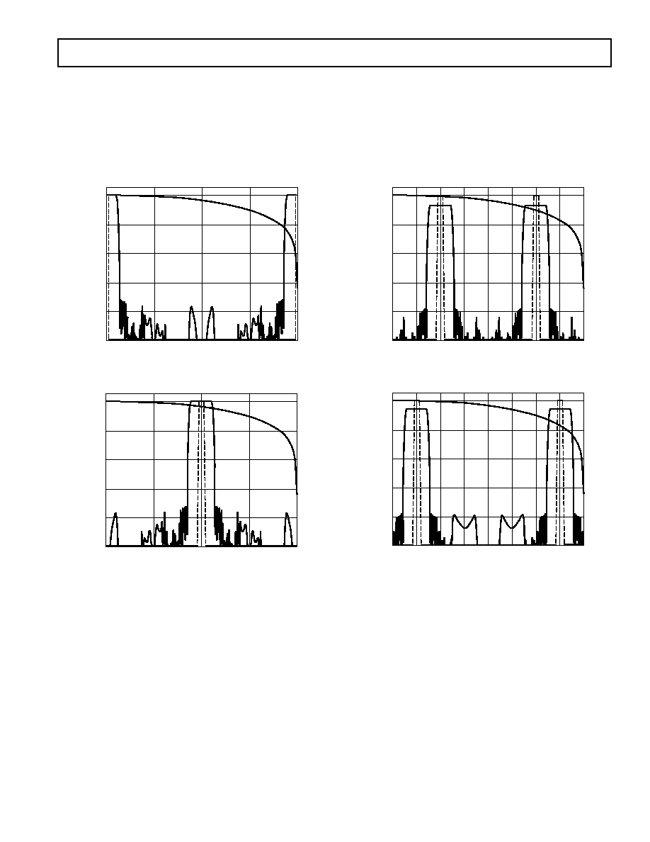
REV. 0
AD9777
≠29≠
f
OUT
(
f
DATA
)
0
1
AMPLITUDE ≠ dBFS
≠100
0
≠80
≠60
≠40
≠20
2
3
4
Figure 28a. 8
◊ Interpolation, Modulation Disabled
f
OUT
(
f
DATA
)
0
1
AMPLITUDE ≠ dBFS
≠100
0
≠80
≠60
≠40
≠20
2
3
4
Figure 28b. 8
◊ Interpolation, Modulation = f
DAC
/2
f
OUT
(
f
DATA
)
0
1
AMPLITUDE ≠ dBFS
≠100
0
≠80
≠60
≠40
≠20
2
3
4
5
6
7
8
Figure 28c. 8
◊ Interpolation, Modulation = f
DAC
/4
f
OUT
(
f
DATA
)
0
1
AMPLITUDE ≠ dBFS
≠100
0
≠80
≠60
≠40
≠20
2
3
4
5
6
7
8
Figure 28d. 8
◊ Interpolation, Modulation = f
DAC
/8
Figure 28. Effect of Digital Modulation on DAC Output Spectrum, Interpolation = 8
◊
MODULATION, INTERPOLATION = 8
◊
With Control Register 01h, Bits 7 and 6, set to "11," the
interpolation rate of the AD9777 is 8
◊. Modulation is achieved
by multiplying successive samples at the interpolation filter
output by the sequence (0, 0.707, 1, 0.707, 0, ≠0.707, ≠1, 0.707).
Figures 28a≠28d represent the spectral response of the AD9777
DAC output with 8
◊ interpolation in the various modulation
modes to a narrow band baseband signal.
Looking at Figures 26 through 29, the user can see how higher
interpolation rates reduce the complexity of the reconstruction
filter needed at the DAC output. It also becomes apparent that
the ability to modulate by f
S
/2, f
S
/4, or f
S
/8 adds a degree of
flexibility in frequency planning.
ZERO STUFFING
(Control Register 01h, Bit 3)
As shown in Figure 29, a "0" or null in the output frequency
response of the DAC (after interpolation, modulation, and DAC
reconstruction) occurs at the final DAC sample rate (f
DAC
).
This is due to the inherent SIN(x)/x roll-off response in the digital-
to-analog conversion. In applications where the desired frequency
content is below f
DAC
/2, this may not be a problem. Note that at
f
DAC
/2 the loss due to SIN(x)/x is 4 dB. In direct RF applica-
tions, this roll-off may be problematic due to the increased
pass-band amplitude variation as well as the reduced amplitude
of the desired signal.
Consider an application where the digital data into the AD9777
represents a baseband signal around f
DAC
/4 with a pass band of
f
DAC
/10. The reconstructed signal out of the AD9777 would
experience only a 0.75 dB amplitude variation over its passband.
However, the image of the same signal occurring at 3
◊ f
DAC
/4
will suffer from a pass-band flatness variation of 3.93 dB. This
image may be the desired signal in an IF application using one
of the various modulation modes in the AD9777. This roll-off
of image frequencies can be seen in Figures 25 through 28,
where the effect of the interpolation and modulation rate is
apparent as well.
REV. 0
≠30≠
AD9777
f
OUT
, NORMALIZED TO
f
DATA
WITH ZERO STUFFING
DISABLED ≠ Hz
SIN (X)
/
X ROLL-OFF ≠ dBFS
0
0
≠50
≠40
≠30
≠20
≠10
0.5
10
1.0
1.5
2.0
ZERO STUFFING
ENABLED
ZERO STUFFING
DISABLED
Figure 29. Effect of Zero Stuffing on DAC's
SIN(x)/x Response
To improve upon the pass-band flatness of the desired image, the
zero stuffing mode can be enabled by setting the control register
bit to a Logic "1." This option increases the ratio of f
DAC
/f
DATA
by a factor of 2 by doubling the DAC sample rate and inserting
a midscale sample (i.e., 1000 0000 0000 0000) after every data
sample originating from the interpolation filter. This is important as
it will affect the PLL divider ratio needed to keep the VCO within
its optimum speed range. Note that the zero stuffing takes place
in the digital signal chain at the output of the digital modulator,
before the DAC.
The net effect is to increase the DAC output sample rate by a
factor of 2
◊ with the "0" in the SIN(x)/x DAC transfer function
occurring at twice the original frequency. A 6 dB loss in amplitude
at low frequencies is also evident, as can be seen in Figure 30.
It is important to realize that the zero stuffing option by itself does
not change the location of the images but rather their amplitude,
pass-band flatness, and relative weighting. For instance, in the
previous example, the pass-band amplitude flatness of the image
at 3
◊ f
DATA
/4 is now improved to 0.59 dB while the signal level
has increased slightly from ≠10.5 dBFS to ≠8.1 dBFS.
INTERPOLATING (COMPLEX MIX MODE)
(Control Register 01h, Bit 2)
In the complex mix mode, the two digital modulators on the
AD9777 are coupled to provide a complex modulation function.
In conjunction with an external quadrature modulator, this
complex modulation can be used to realize a transmit image
rejection architecture. The complex modulation function can be
programmed for e
+j t
or
e
≠j t
to give upper or lower image rejec-
tion. As in the real modulation mode, the modulation frequency
can be programmed via the SPI port for f
DAC
/2, f
DAC
/4, and
f
DAC
/8, where f
DAC
represents the DAC output rate.
OPERATIONS ON COMPLEX SIGNALS
Truly complex signals cannot be realized outside of a computer
simulation. However, two data channels, both consisting of real
data, can be defined as the real and imaginary components of a
complex signal. I (real) and Q (imaginary) data paths are often
defined this way. By using the architecture defined in Figure 30,
a system that operates on complex signals can be realized,
giving a complex (real and imaginary) output.
If a complex modulation function (e
+j t
) is desired, the real and
imaginary components of the system correspond to the real and
imaginary components of e
+j t
, or cos t and sin t. As Figure 31
shows, the complex modulation function can be realized by
applying these components to the structure of the complex
system defined in Figure 30.
a(t)
INPUT
INPUT
OUTPUT
OUTPUT
COMPLEX FILTER
= (c + jd)
IMAGINARY
b(t)
b(t)
a(t) + c
b(t)
c(t)
b(t) + d
b(t)
Figure 30. Realization of a Complex System
90
OUTPUT
(IMAGINARY)
OUTPUT
(REAL)
INPUT
(REAL)
INPUT
(IMAGINARY)
e
≠j t
= COS t + jSIN t
Figure 31. Implementation of a Complex Modulator
COMPLEX MODULATION AND IMAGE REJECTION OF
BASEBAND SIGNALS
In traditional transmit applications, a two-step upconversion is
done in which a baseband signal is modulated by one carrier to
an IF (intermediate frequency) and then modulated a second
time to the transmit frequency. Although this approach has
several benefits, a major drawback is that two images are created
near the transmit frequency. Only one image is needed, the other
being an exact duplicate. Unless the unwanted image is filtered,
typically with analog components, transmit power is wasted and
the usable bandwidth available in the system is reduced.
A more efficient method of suppressing the unwanted image
can be achieved by using a complex modulator followed by a
quadrature modulator. Figure 32 is a block diagram of a quadra-
ture modulator. Note that it is in fact the real output half of a
complex modulator. The complete upconversion can actually be
referred to as two complex upconversion stages, the real output
of which becomes the transmitted signal.
90
OUTPUT
INPUT
(REAL)
INPUT
(IMAGINARY)
COS t
SIN t
Figure 32. Quadrature Modulator
REV. 0
AD9777
≠31≠
The entire upconversion from baseband to transmit frequency is
represented graphically in Figure 33. The resulting spectrum
shown in Figure 33 represents the complex data consisting of
the baseband real and imaginary channels, now modulated onto
orthogonal (cosine and negative sine) carriers at the transmit
frequency. It is important to remember that in this application
(two baseband data channels), the image rejection is not
dependent on the data at either of the AD9777 input channels.
In fact, image rejection will still occur with either one or both of
the AD9777 input channels active. Note that by changing the
sign of the sinusoidal multiplying term in the complex modula-
tor, the upper sideband image could have been suppressed while
passing the lower one. This is easily done in the AD9777 by
selecting the e
+j t
bit (Register 01h, Bit 1). In purely complex
terms, Figure 31 represents the two-stage upconversion from
complex baseband to carrier.
REAL CHANNEL (IN)
IMAGINARY CHANNEL (IN)
DC
DC
A
B
COMPLEX
MODULATOR
REAL CHANNEL (OUT)
IMAGINARY CHANNEL (OUT)
≠F
C
*
B/2J
≠B/2J
TO QUADRATURE
MODULATOR
≠F
C
≠F
C
≠F
C
F
C
F
C
≠F
C
F
C
A/2J
≠A/2J
B/2
B/2
A/2
A/2
REAL
IMAGINARY
QUADRATURE
MODULATOR
OUT
A/4 + B/4J
A/4 ≠ B/4J
≠F
Q
≠ F
C
REJECTED IMAGES
A/4 + B/4J
A/4 ≠ B/4J
A/4 + B/4J
A/4 ≠ B/4J
≠A/4 ≠ B/4J
≠A/4 + B/4J
A/2 + B/2J
A/2 ≠ B/2J
≠F
Q
*
≠F
Q
+ F
C
F
Q
≠ F
C
F
Q
F
Q
+ F
C
≠F
Q
F
Q
≠F
Q
F
Q
*FC = COMPLEX MODULATION FREQUENCY
*FQ = QUADRATURE MODULATION FREQUENCY
Figure 33. Two-Stage Upconversion and Resulting Image Rejection

REV. 0
≠32≠
AD9777
OUTPUT = REAL
COMPLEX BASEBAND
SIGNAL
DC
= REAL
ej( 1 + 2)t
FREQUENCY
≠ 1 ≠ 2
1 + 2
1
1/2
1/2
Figure 34. Two-Stage Complex Upconversion
IMAGE REJECTION AND SIDEBAND SUPPRESSION OF
MODULATED CARRIERS
As shown in Figure 33, image rejection can be achieved by applying
baseband data to the AD9777 and following the AD9777 with a
quadrature modulator. To process multiple carriers while still
maintaining image reject capability, each carrier must be complex
modulated. As Figure 34 shows, single- or multiple-complex
modulators can be used to synthesize complex carriers. These
complex carriers are then summed and applied to the real and
imaginary inputs of the AD9777. A system in which multiple
baseband signals are complex modulated and then applied to the
AD9777 real and imaginary inputs, followed by a quadrature
modulator is shown in Figure 36, which also describes the transfer
function of this system and the spectral output. Note the similarity
of the transfer functions given in Figure 36 and Figure 34. Fig-
ure 36 adds an additional complex modulator stage for the purpose
of summing multiple carriers at the AD9777 inputs. Also, as in
Figure 33, the image rejection is not dependent on the real or
imaginary baseband data on any channel. Image rejection on a
channel will occur if either the real or imaginary data, or both, is
present on the baseband channel.
It is important to remember that the magnitude of a complex signal
can be 1.414
◊ the magnitude of its real or imaginary components. Due
to this 3 dB increase in signal amplitude, the real and imaginary inputs
to the AD9777 must be kept at least 3 dB below full scale when
operating with the complex modulator. Overranging in the com-
plex modulator will result in severe distortion at the DAC output.
R(1)
BASEBAND CHANNEL 1
REAL INPUT
IMAGINARY INPUT
R(1)
COMPLEX
MODULATOR 1
BASEBAND CHANNEL N
REAL INPUT
IMAGINARY INPUT
COMPLEX
MODULATOR N
R(N)
R(N)
BASEBAND CHANNEL 2
REAL INPUT
IMAGINARY INPUT
R(2)
R(2)
COMPLEX
MODULATOR 2
R(N) = REAL OUTPUT OF N
I(N) = IMAGINARY OUTPUT OF N
MULTICARRIER
REAL OUTPUT =
R(1) + R(2) +...R(N)
(TO REAL INPUT OF AD9777)
MULTICARRIER
IMAGINARY OUTPUT =
I(1) + I(2) +...I(N)
(TO IMAGINARY INPUT OF AD9777)
Figure 35. Synthesis of Multicarrier Complex Signal
REAL
IMAGINARY
MULTIPLE
COMPLEX
MODULATORS
FREQUENCY =
1
,
2
...
N
REAL
IMAGINARY
REAL
IMAGINARY
AD9777
COMPLEX
MODULATOR
FREQUENCY =
C
QUADRATURE
MODULATOR
FREQUENCY =
Q
MULTIPLE
BASEBAND
CHANNELS
REAL
REJECTED IMAGES
DC
≠
1
≠
C
≠
Q
1
+
C
+
Q
OUTPUT = REAL
ej(
N
+
C
+
Q
)t
COMPLEX BASEBAND
SIGNAL
Figure 36. Image Rejection with Multicarrier Signals

REV. 0
AD9777
≠33≠
The complex carrier synthesized in the AD9777 digital modulator
is accomplished by creating two real digital carriers in quadrature.
Carriers in quadrature cannot be created with the modulator
running at f
DAC
/2. As a result, complex modulation only func-
tions with modulation rates of f
DAC
/4 and f
DAC
/8.
Regions A and B of Figures 37 through 42 are the result of the
complex signal described above, when complex modulated in the
AD9777 by +e
j t
. Regions C and D are the result of the complex
signal described above, again with positive frequency components
only, modulated in the AD9777 by ≠e
j t
. The analog quadrature
modulator after the AD9777 inherently modulates by +e
j t
.
Region A
Region A is a direct result of the upconversion of the complex
signal near baseband. If viewed as a complex signal, only the
images in Region A will remain. The complex Signal A, consist-
ing of positive frequency components only in the digital domain,
has images in the positive odd Nyquist zones (1, 3, 5...) as well
as images in the negative even Nyquist zones. The appearance
and rejection of images in every other Nyquist zone will become
more apparent at the output of the quadrature modulator. The
A images will appear on the real and the imaginary outputs of the
AD9777, as well as on the output of the quadrature modulator,
where the center of the spectral plot will now represent the
quadrature modulator LO and the horizontal scale now repre-
sents the frequency offset from this LO.
Region B
Region B is the image (complex conjugate) of Region A. If a
spectrum analyzer is used to view the real or imaginary DAC
outputs of the AD9777, Region B will appear in the spectrum.
However, on the output of the quadrature modulator, Region B
will be rejected.
Region C
Region C is most accurately described as a down conversion, as
the modulating carrier is ≠e
j t
. If viewed as a complex signal, only
the images in Region C will remain. This image will appear on the
real and imaginary outputs of the AD9777, as well as on the
output of the quadrature modulator, where the center of the
spectral plot will now represent the quadrature modulator LO
and the horizontal scale will represent the frequency offset
from this LO.
Region D
Region D is the image (complex conjugate) of Region C. If a
spectrum analyzer is used to view the real or imaginary DAC
outputs of the AD9777, Region D will appear in the spectrum.
However, on the output of the quadrature modulator, Region D
will be rejected.
Figures 43 through 50 show the measured response of the AD9777
and AD8345 given the complex input signal to the AD9777 in
Figure 43. The data in these graphs was taken with a data rate of
12.5 MSPS at the AD9777 inputs. The interpolation rate of 4
◊
or 8
◊ gives a DAC output data rate of 50 MSPS or 100 MSPS.
As a result, the high end of the DAC output spectrum in these
graphs is the first null point for the SIN(x)/x roll-off, and the
asymmetry of the DAC output images is representative of the
SIN(x)/x roll-off over the spectrum. The internal PLL was enabled
for these results. In addition, a 35 MHz third order low-pass filter
was used at the AD9777/AD8345 interface to suppress DAC images.
An important point can be made by looking at Figures 45 and 47.
Figure 45 represents a group of positive frequencies modulated
by complex +f
DAC
/4, while Figure 47 represents a group of nega-
tive frequencies modulated by complex ≠f
DAC
/4. When looking at
the real or imaginary outputs of the AD9777, as shown in Fig-
ures 45 and 47, the results look identical. However, the spectrum
analyzer cannot show the phase relationship of these signals. The
difference in phase between the two signals becomes apparent
when they are applied to the AD8345 quadrature modulator,
with the results shown in Figures 46 and 48.
REV. 0
≠34≠
AD9777
D
A
B
C
D
A
B
C
f
OUT
(
f
DATA
)
≠2.0
≠100
≠80
≠60
≠40
≠20
0
≠1.5
≠1.0
≠0.5
0
0.5
1.0
1.5
2.0
(LO)
Figure 37. 2
◊ Interpolation, Complex f
DAC
/4 Modulation
D
A
B
C
D
A
B
C
f
OUT
(
f
DATA
)
≠4.0
≠100
≠80
≠60
≠40
≠20
0
≠3.0
≠2.0
≠1.0
0
1.0
2.0
3.0
4.0
(LO)
Figure 38. 4
◊ Interpolation, Complex f
DAC
/4 Modulation
D
A
B
C
D
A
B
C
f
OUT
(
f
DATA
)
≠8.0
≠100
≠80
≠60
≠40
≠20
0
≠6.0
≠4.0
≠2.0
0
2.0
4.0
6.0
8.0
(LO)
Figure 39. 8
◊ Interpolation, Complex f
DAC
/4 Modulation
A
B
C D
A
B
f
OUT
(
f
DATA
)
≠2.0
≠100
≠80
≠60
≠40
≠20
0
≠1.5
≠1.0
≠0.5
0
0.5
1.0
1.5
2.0
(LO)
C
D
Figure 40. 2
◊ Interpolation, Complex f
DAC
/8 Modulation
A
B
C D
A
B
f
OUT
(
f
DATA
)
≠4.0
≠100
≠80
≠60
≠40
≠20
0
≠3.0
≠2.0
≠1.0
0
1.0
2.0
3.0
4.0
(LO)
C
D
Figure 41. 4
◊ Interpolation, Complex f
DAC
/8 Modulation
f
OUT
(
f
DATA
)
≠8.0
≠100
≠80
≠60
≠40
≠20
0
≠6.0
≠4.0
≠2.0
0
2.0
4.0
6.0
8.0
(LO)
A
D
C
B
A
D
C
B
Figure 42. 8
◊ Interpolation, Complex f
DAC
/8 Modulation
REV. 0
AD9777
≠35≠
AMPLITUDE ≠ dBm
≠30
≠100
0
10
50
20
≠60
≠70
≠90
≠80
≠40
≠50
≠20
FREQUENCY ≠ MHz
≠10
0
30
40
Figure 43. AD9777, Real DAC Output of Complex
Input Signal Near Baseband (Positive Frequencies
Only), Interpolation = 4 , No Modulation in AD9777
AMPLITUDE ≠ dBm
≠30
≠100
≠60
≠70
≠90
≠80
≠40
≠50
≠20
≠10
0
750
FREQUENCY ≠ MHz
760
770
780
790
800
810
820
830
840
850
Figure 44. AD9777 Complex Output from
Figure 43, Now Quadrature Modulated
by AD8345 (LO = 800 MHz)
AMPLITUDE ≠ dBm
≠30
≠100
0
20
40
≠60
≠70
≠90
≠80
≠40
≠50
≠20
FREQUENCY ≠ MHz
≠10
0
30
50
10
Figure 45. AD9777, Real DAC Output of Complex
Input Signal Near Baseband (Positive Frequencies
Only), Interpolation = 4 , Complex Modulation in
AD9777 = +f
DAC
/4
AMPLITUDE ≠ dBm
≠30
≠100
≠60
≠70
≠90
≠80
≠40
≠50
≠20
≠10
0
750
FREQUENCY ≠ MHz
760
770
780
790
800
810
820
830
840
850
Figure 46. AD9777 Complex Output from Figure
Figure 45, Now Quadrature Modulated by AD8345
(LO = 800 MHz)
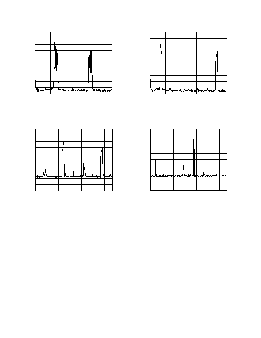
REV. 0
≠36≠
AD9777
AMPLITUDE ≠ dBm
≠30
≠100
0
20
40
≠60
≠70
≠90
≠80
≠40
≠50
≠20
FREQUENCY ≠ MHz
≠10
0
30
50
10
Figure 47. AD9777, Real DAC Output of Complex
Input Signal Near Baseband (Negative Frequencies
Only), Interpolation = 4 , Complex Modulation in
AD9777 = ≠f
DAC
/4
AMPLITUDE ≠ dBm
≠30
≠100
≠60
≠70
≠90
≠80
≠40
≠50
≠20
≠10
0
750
FREQUENCY ≠ MHz
760
770
780
790
800
810
820
830
840
850
Figure 48. AD9777 Complex Output from
Figure 47, Now Quadrature Modulated by
AD8345 (LO = 800 MHz)
AMPLITUDE ≠ dBm
≠30
≠100
≠60
≠70
≠90
≠80
≠40
≠50
≠20
≠10
0
0
20
80
40
FREQUENCY ≠ MHz
60
100
Figure 49. AD9777, Real DAC Output of Complex
Input Signal Near Baseband (Positive Frequencies
Only), Interpolation = 8 , Complex Modulation in
AD9777 = +f
DAC
/8
AMPLITUDE ≠ dBm
≠30
≠100
≠60
≠70
≠90
≠80
≠40
≠50
≠20
≠10
0
700
FREQUENCY ≠ MHz
720
740
760
780
800
820
840
860
880
900
Figure 50. AD9777 Complex Output from
Figure 49, Now Quadrature Modulated by
AD8345 (LO = 800 MHz)
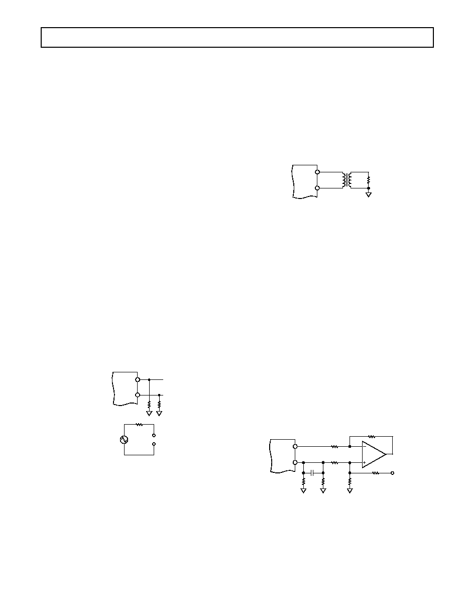
REV. 0
AD9777
≠37≠
DIFFERENTIAL COUPLING USING A TRANSFORMER
An RF transformer can be used to perform a differential-to-
single-ended signal conversion as shown in Figure 52. A
differentially coupled transformer output provides the optimum
distortion performance for output signals whose spectral content
lies within the transformer's pass band. An RF transformer,
such as the Mini-Circuits T1-1T, provides excellent rejection
of common-mode distortion (i.e., even-order harmonics) and
noise over a wide frequency range. It also provides electrical
isolation and the ability to deliver twice the power to the load.
Transformers with different impedance ratios may also be used
for impedance matching purposes.
I
OUTA
I
OUTB
DAC
R
LOAD
MINI-CIRCUITS
T1-T2
Figure 52. Transformer-Coupled Output Circuit
The center tap on the primary side of the transformer must be
connected to AGND to provide the necessary dc current path
for both I
OUTA
and I
OUTB
. The complementary voltages appearing
at I
OUTA
and I
OUTB
(i.e., V
OUTA
and V
OUTB
) swing symmetrically
around AGND and should be maintained within the specified
output compliance range of the AD9777. A differential resistor,
R
DIFF
, may be inserted in applications where the output of the
transformer is connected to the load, R
LOAD
, via a passive recon-
struction filter or cable. R
DIFF
is determined by the transformer's
impedance ratio and provides the proper source termination
that results in a low VSWR. Note that approximately half the
signal power will be dissipated across R
DIFF
.
DIFFERENTIAL COUPLING USING AN OP AMP
An op amp can also be used to perform a differential-to-single-
ended conversion as shown in Figure 53. This has the added
benefit of providing signal gain as well. In Figure 53, the AD9777
is configured with two equal load resistors, R
LOAD
, of 25
. The
differential voltage developed across I
OUTA
and I
OUTB
is converted
to a single-ended signal via the differential op amp configuration.
An optional capacitor can be installed across I
OUTA
and I
OUTB
,
forming a real pole in a low-pass filter. The addition of this
capacitor also enhances the op amp's distortion performance by
preventing the DAC's fast slewing output from overloading the
input of the op amp.
I
OUTA
I
OUTB
DAC
25
AD8021
500
C
OPT
225
225
500
R
OPT
225
AVDD
25
Figure 53. Op Amp-Coupled Output Circuit
The common-mode (and second order distortion) rejection of this
configuration is typically determined by the resistor matching. The
op amp used must operate from a dual supply since its output
is approximately
± 1.0 V. A high speed amplifier, such as the
AD8021, capable of preserving the differential performance of the
APPLYING THE AD9777 OUTPUT CONFIGURATIONS
The following sections illustrate typical output configurations for
the AD9777. Unless otherwise noted, it is assumed that I
OUTFS
is set to a nominal 20 mA. For applications requiring optimum
dynamic performance, a differential output configuration is
suggested. A simple differential output may be achieved by
converting I
OUTA
and I
OUTB
to a voltage output by terminating
them to AGND via equal value resistors. This type of configura-
tion may be useful when driving a differential voltage input device
such as a modulator. If a conversion to a single-ended signal is
desired and the application allows for ac-coupling, an RF trans-
former may be useful; if power gain is required, an op amp may
be used. The transformer configuration provides optimum high
frequency noise and distortion performance. The differential op
amp configuration is suitable for applications requiring dc-
coupling, signal gain, and/or level shifting within the bandwidth of
the chosen op amp.
A single-ended output is suitable for applications requiring a
unipolar voltage output. A positive unipolar output voltage will
result if I
OUTA
and/or I
OUTB
is connected to a load resistor,
R
LOAD
, referred to AGND. This configuration is most suitable
for a single-supply system requiring a dc-coupled, ground
referred output voltage. Alternatively, an amplifier could be
configured as an I-V converter, thus converting I
OUTA
or I
OUTB
into a negative unipolar voltage. This configuration provides
the best DAC dc linearity as I
OUTA
or I
OUTB
are maintained at
ground or virtual ground.
UNBUFFERED DIFFERENTIAL OUTPUT, EQUIVALENT
CIRCUIT
In many applications, it may be necessary to understand the
equivalent DAC output circuit. This is especially useful when
designing output filters or when driving inputs with finite input
impedances. Figure 51 illustrates the output of the AD9777 and
the equivalent circuit. A typical application where this informa-
tWn may be useful is when designing an interface filter between the
AD9777 and Analog Devices' AD8345 quadrature modulator.
I
OUTA
R
A
+ R
B
I
OUTB
V
OUT
(DIFFERENTIAL)
V
SOURCE
=
I
OUTFS
(R
A
+ R
B
)
p-p
V
OUT
+
V
OUT
≠
Figure 51. DAC Output Equivalent Circuit
For the typical situation, where I
OUTFS
= 20 mA and R
A
and R
B
both equal 50
, the equivalent circuit values become:
V
SOURCE
= 2 V p-p
R
OUT
= 100
Note that the output impedance of the AD9777 DAC itself is
greater than 100 k
and typically has no effect on the imped-
ance of the equivalent output circuit.
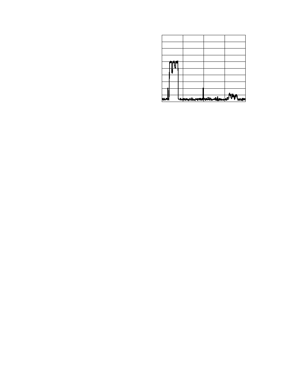
REV. 0
≠38≠
AD9777
FREQUENCY ≠ MHz
AMPLITUDE ≠ dBm
≠80
0
762.5
≠70
≠60
≠50
≠40
≠30
≠20
≠10
≠90
≠100
782.5
802.5
822.5
842.5
Figure 54. AD9777/AD8345 Synthesizing a Three
Carrier WCDMA Signal at an LO of 800 MHz
EVALUATION BOARD
The AD9777 evaluation board allows easy configuration of the
various modes, programmable via the SPI port. Software is available
for programming the SPI port from either Win95
Æ
or Win98
Æ
. The
evaluation board also contains an AD8345 quadrature modu-
lator and support circuitry that allows the user to optimally
configure the AD9777 in an image reject transmit signal chain.
Figures 55 through 58 describe how to configure the evaluation
board in the one and two port input modes with the PLL enabled
and disabled. Refer to Figures 59 through 68, the schematics, and
the layout for the AD9777 evaluation board for the jumper loca-
tions described below. The AD9777 outputs can be configured
for various applications by referring to the following instructions.
DAC Single-Ended Outputs
Remove transformers T2 and T3. Solder jumper link JP4 or
JP28 to look at the DAC1 outputs. Solder jumper link JP29 or
JP30 to look at the DAC2 outputs. Jumpers 8 and 13≠17 should
remain unsoldered. The jumpers JP35≠JP38 may be used to
ground one of the DAC outputs while the other is measured
single-ended. Optimum single-ended distortion performance is
typically achieved in this manner. The outputs are taken from
S3 and S4.
DAC Differential Outputs
Transformers T2 and T3 should be in place. Note that the lower
band of operation for these transformers is 300 kHz to 500 kHz.
Jumpers 4, 8, 13≠17, and 28≠30 should remain unsoldered. The
outputs are taken from S3 and S4.
Using the AD8345
Remove transformers T2 and T3. Jumpers JP4 and 28≠30 should
remain unsoldered. Jumpers 13≠16 should be soldered. The
desired components for the low pass interface filters L6, L7,
C55, and C81 should be in place. The LO drive is connected to
the AD8345 via J10 and the balun T4, and the AD8345 output
is taken from J9.
Win95 and Win98 are a registered trademarks of Microsoft Corporation.
AD9777 while meeting other system level objectives (i.e., cost,
power) is recommended. The op amp's differential gain, gain
setting resistor values, and full-scale output swing capabilities
should all be considered when optimizing this circuit. R
OPT
is
only necessary if level shifting is required on the op amp output.
In Figure 53, AVDD, which is the positive analog supply for
both the AD9777 and the op amp, is also used to level shift the
differential output of the AD9777 to midsupply (i.e., AVDD/2).
INTERFACING THE AD9777 WITH THE AD8345
QUADRATURE MODULATOR
The AD9777 architecture was defined to operate in a transmit
signal chain using an image reject architecture. A quadrature
modulator is also required in this application and should be
designed to meet the output characteristics of the DAC as much
as possible. The AD8345 from Analog Devices meets many of
the requirements for interfacing with the AD9777. As with any
DAC output interface, there are a number of issues that have to
be resolved. Among the major issues are the following.
DAC Compliance Voltage/Input Common-Mode Range
The dynamic range of the AD9777 is optimal when the DAC
outputs swing between
±1.0 V. The input common-mode range
of the AD8345, at 0.7 V, allows optimum dynamic range to be
achieved in both components.
Gain/Offset Adjust
The matching of the DAC output to the common-mode input
of the AD8345 allows the two components to be dc-coupled,
with no level shifting necessary. The combined voltage offset of
the two parts can therefore be compensated for via the AD9777
programmable offset adjust. This allows excellent LO cancella-
tion at the AD8345 output. The programmable gain adjust
allows for optimal image rejection as well.
The AD9777 evaluation board includes an AD8345 and recom-
mended interface (Figures 59 and 60). On the output of the
AD9777, R9 and R10 convert the DAC output current to a voltage.
R16 may be used to do a slight common-mode shift if necessary.
The (now voltage) signal is applied to a low pass reconstruction
filter to reject DAC images. The components installed on the
AD9777 provide a 35 MHz cutoff, but may be changed to fit
the application. A balun (Mini-Circuits ADTL1-12) is used to
cross the ground plane boundary to the AD8345. Another balun
(Mini-Circuits ETC1-1-13) is used to couple the LO input of
the AD8345. The interface requires a low ac impedance return
path from the AD8345, so a single connection between the
AD9777 and AD8345 ground planes is recommended.
The performance of the AD9777 and AD8345 in an image reject
transmitter, reconstructing three WCDMA carriers, can be seen in
Figure 54. The LO of the AD8345 in this application is 800 MHz.
Image rejection (50 dB) and LO feedthrough (≠78 dBFS) have
been optimized with the programmable features of the AD9777.
The average output power of the digital waveform for this test was
set to ≠15 dBFS to account for the peak-to-average ratio of the
WCDMA signal.
REV. 0
AD9777
≠39≠
SIGNAL GENERATOR
CLK+/CLK≠
DATACLK
LECROY
PULSE
GENERATOR
TRIG
INP
AWG2021
OR
DG2020
INPUT CLOCK
DAC1, DB11≠DB0
AD9777
DAC2, DB11≠DB0
40-PIN RIBBON CABLE
JUMPER CONFIGURATION FOR TWO PORT MODE PLL ON
SOLDERED/IN
UNSOLDERED/OUT
JP1 -
JP2 ≠
JP3 ≠
JP5 ≠
JP6 ≠
JP12 ≠
JP24 ≠
JP25 ≠
JP26 ≠
JP27 ≠
JP31 ≠
JP32 ≠
JP33 ≠
Figure 55. Test Configuration for AD9777 in Two Port Mode with PLL Enabled, Signal Generator
Frequency = Input Data Rate, DAC Output Data Rate = Signal Generator Frequency Interpolation Rate
SIGNAL GENERATOR
CLK+/CLK≠
ONEPORTCLK
LECROY
PULSE
GENERATOR
TRIG
INP
AWG2021
OR
DG2020
INPUT CLOCK
DAC1, DB11≠DB0
AD9777
DAC2, DB11≠DB0
JUMPER CONFIGURATION FOR TWO PORT MODE PLL ON
SOLDERED/IN
UNSOLDERED/OUT
JP1 ≠
JP2 ≠
JP3 ≠
JP5 ≠
JP6 ≠
JP12 ≠
JP24 ≠
JP25 ≠
JP26 ≠
JP27 ≠
JP31 ≠
JP32 ≠
JP33 ≠
Figure 56. Test Configuration for AD9777 in One Port Mode with PLL Enabled, Signal Generator
Frequency = One-Half Interleaved Input Data Rate, ONEPORTCLK = Interleaved Input Data Rate, DAC Output
Data Rate = Signal Generator Frequency Interpolation Rate
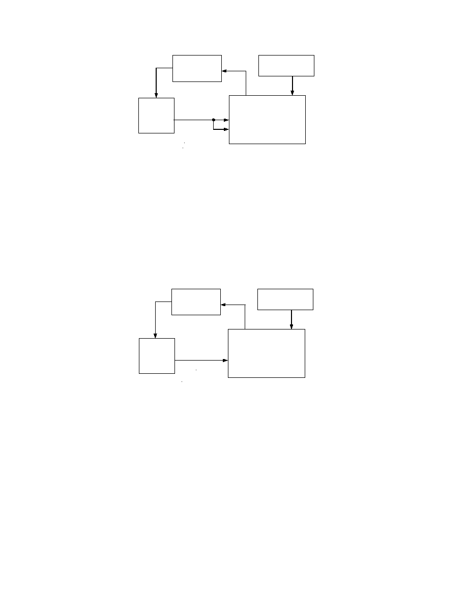
REV. 0
≠40≠
AD9777
SIGNAL GENERATOR
CLK+/CLK≠
DATACLK
LECROY
PULSE
GENERATOR
TRIG
INP
AWG2021
OR
DG2020
INPUT CLOCK
DAC1, DB11≠DB0
AD9777
DAC2, DB11≠DB0
40-PIN RIBBON CABLE
JUMPER CONFIGURATION FOR TWO PORT MODE PLL OFF
SOLDERED/IN
UNSOLDERED/OUT
JP1 ≠
JP2 ≠
JP3 ≠
JP5 ≠
JP6 ≠
JP12 ≠
JP24 ≠
JP25 ≠
JP26 ≠
JP27 ≠
JP31 ≠
JP32 ≠
JP33 ≠
Figure 57. Test Configuration for AD9777 in Two Port Mode with PLL Disabled, DAC Output Data Rate = Signal
Generator Frequency, DATACLK = Signal Generator Frequency/Interpolation Rate
SIGNAL GENERATOR
CLK+/CLK≠
ONEPORTCLK
LECROY
PULSE
GENERATOR
TRIG
INP
AWG2021
OR
DG2020
INPUT CLOCK
DAC1, DB11≠DB0
AD9777
DAC2, DB11≠DB0
JUMPER CONFIGURATION FOR TWO PORT MODE PLL ON
SOLDERED/IN
UNSOLDERED/OUT
JP1 ≠
JP2 ≠
JP3 ≠
JP5 ≠
JP6 ≠
JP12 ≠
JP24 ≠
JP25 ≠
JP26 ≠
JP27 ≠
JP31 ≠
JP32 ≠
JP33 ≠
Figure 58. Test Configuration for AD9777 in One Port Mode with PLL Disabled, DAC Output Data
Rate = Signal Generator Frequency, ONEPORTCLK = Interleaved Input Data Rate = 2
Signal Generator
Frequency/Interpolation Rate

REV. 0
AD9777
≠41≠
JP18
VDDMIN
VDDM
J10
DGND; 3, 4, 5
16
15
14
13
12
11
10
9
1
2
3
4
5
6
7
8
S
P
T6
ADTL1-12
S
P
1
3
4
6
4
6
1
3
C78
0.1 F
C75
0.1 F
C35
10 F
C72
10 F
10V
P
S
C78
0.1 F
1
3
4
5
C77
100pF
T5
ADTL1-12
T4
ETC1-1-13
R30
DNP
R28
0
LOCAL OSC INPUT
R26
1k
J7
J21
C74
100pF
J10
DGND; 3, 4, 5
MODULATED OUTPUT
R23
0
R33
51
R34
DNP
C79
DNP
J19
R32
51
C81
DNP
C55
DNP
O2P
L7
DNP
L6
DNP
R36
51
R37
DNP
C80
DNP
J20
R35
51
C73
DNP
C54
DNP
O1P
L5
DNP
L4
DNP
O1N
O2N
DVDD_IN
J8
AGND
C65
22 F
16V
J5
C67
0.1 F
C66
22 F
16V
J9
L3 FERRITE
TP2
RED
DVDD
TP3
BLK
AVDD_IN
J4
AGND
C64
22 F
16V
J6
C68
0.1 F
C61
22 F
16V
J10
L2 FERRITE
TP4
RED
AVDD
TP5
BLK
CLKVDD_IN
J3
AGND
C63
22 F
16V
J7
C69
0.1 F
C62
22 F
16V
J11
L1 FERRITE
TP6
RED
CLKVDD
TP7
BLK
VDDMIN
W11
C28
22 F
16V
W12
C32
0.1 F
L8 FERRITE
VDDM
POWER INPUT FILTERS
Figure 59. AD8345 Circuitry on AD9777 Evaluation Board
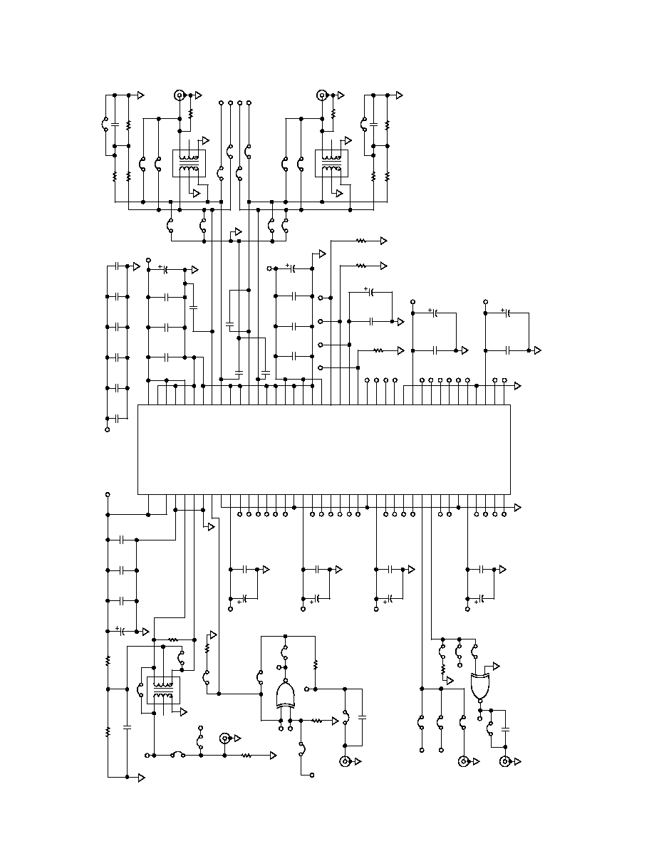
REV. 0
≠42≠
AD9777
TP14
WHT
BD08
BD09
BD10
BD11
BD12
BD13
AD00
AD01
AD03
AD04
AD05
AD07
AD08
AD09
AD10
AD11
AD12
AD13
AD14
AD15
AD06
AD02
O1N
O1P
O2N
O2P
U1
AD9777
CLKN
CLKP
DCLK-PLLL
FSADJ1
FSADJ2
IOUT1N
IOUT1P
IOUT2N
IOUT2P
P1D0
P1D1
P1D10
P1D11
P1D12
P1D13
P1D14
P1D15
P1D2
P1D3
P1D4
P1D5
P1D6
P1D7
P1D8
P1D9
P2D0
P2D1
P2D10
P2D11
P2D12
P2D13
P2D14-OPCLK
P2D15-IQSEL
P2D2
P2D3
P2D4
P2D5
P2D6
P2D7
P2D8
P2D9
REFOUT
RESET
SP-CLK
SP-CSB
SP-SDO
SP-SDI
VDDA1
VDDA2
VDDA3
VDDA4
VDDA5
VDDA6
VDDC1
VDDC2
VDDD1
VSSD2
VDDD3
VDDD4
VDDD5
VDDD6
VSSA1
VSSA10
VSSA2
VSSA3
VSSA4
VSSA5
VSSA6
VSSA7
VSSA8
VSSA9
VSSC1
VSSC2
VSSD1
VDDD2
VSSD3
VSSD4
VSSD5
VSSD6
1
2
3
4
5
6
7
8
9
10
11
12
13
14
15
16
17
18
19
20
21
22
23
24
25
26
27
28
29
30
31
32
33
34
35
36
37
38
39
40
80
79
78
77
76
75
74
73
72
71
70
69
68
67
66
65
64
63
62
61
60
59
58
57
56
55
54
53
52
51
50
49
48
47
46
45
44
43
42
41
LF
C59, DNP
C57, DNP
SPSDO
SPSDI
SPCLK
SPCSP
BD03
BD02
BD01
BD00
BD04
BD05
BD06
BD07
R6
1k
C21
0.001
F
C5
10
F
6.3V
DVDD
C22
0.001
F
C6
10
F
6.3V
DVDD
TP11
WHT
TP10
WHT
TP9
WHT
TP8
WHT
C16
0.1
F
C4
10
F
6.3V
R7
2k
C18
0.1
F
R8
2k
C17
0.1
F
C15
0.1
F
C3
10
F
6.3V
C58, DNP
AVDD
C58, DNP
C20
0.1
F
C19
0.1
F
C14
0.1
F
C2
10
F
6.3V
AVDD
3
2
1
4
5
6
J37
J35
J36
J38
J13
J15
J16
J14
J28
T2
T1-1T
J4
R9, 51
R10, 51
J8
C70, 0.1
F
R16, 10
R42
49.9
S3
3
2
1
4
5
6
J30
T3
T1-1T
J29
R43
49.9
S4
OUT1
OUT2
R11, 51
R12, 51
J17
C70, 0.1
F
R17, 10
AGND;3,4,5
AGND;3,4,5
C36
0.1
F
C37
0.1
F
C38
0.1
F
C39
0.1
F
C40
0.1
F
C41
0.1
F
DVDD
C12
0.1
F
C11
0.1
F
C42
0.1
F
C1
10
F
6.3V
CLKVDD
C26
0.001
F
C10
10
F
6.3V
DVDD
C25
0.001
F
C9
10
F
6.3V
DVDD
C24
0.001
F
C8
10
F
6.3V
DVDD
C23
0.001
F
C7
10
F
6.3V
DVDD
3
2
1
4
5
6
T1
T1-1T
R1
200
J23
J22
R3
1k
R2
1k
C13
0.1
F
R38, 10k
J33
J24
J25
11
CX3
R5
49.9
DVDD; 14
AGND; 7
12
13
CX2
CX1
J12
DVDD
R40
200
J1
ADCLK
CLKIN
R4
49.9
TP15
WHT
J2
J3
DATACLK
S2
C29
0.1
F
J5
AGND;3,4,5
BD15
J40
OPCLK_3
J27
S6
AGND;3,4,5
IQ
S5
IQ
OPCLK
AGND;3,4,5
C45
0.01
F
J34
OPCLK
11
J31
J26
J32
BD14
R39
1k
12
13
74VCX86
74VCX86
S1
AGND;3,4,5
Figure 60. AD9777 Clock, Power Supplies, and Output Circuitry
REV. 0
AD9777
≠43≠
RP1, 22
AD15
AD14
AD13
AD12
AD11
AD10
AD09
AD08
AD07
AD06
AD05
AD04
AD03
AD02
AD01
AD00
2
4
6
8
10
12
14
16
18
20
22
24
26
28
30
32
34
36
38
40
1
3
5
7
9
11
13
15
17
19
21
23
25
27
29
31
33
35
37
39
11
6
RP1, 22
21
5
RIBBON
R2
2
1
R3
3
R4
4
R5
5
R6
6
R7
7
R8
8
R9
9
10
R1
RCON
R1
1
R2
2
R3
3
R4
4
R5
5
R6
6
R7
7
R8
8
9
R9
10
RCON
RP5
50
RP1, 22
31
4
RP1, 22
41
3
RP1, 22
51
2
RP1, 22
61
1
RP1, 22
71
0
RP2, 22
89
RP2, 22
11
6
RP2, 22
21
5
RP2, 22
31
4
RP2, 22
41
3
RP2, 22
51
2
RP2, 22
61
1
RP2, 22
71
0
RP2, 22
89
R1
2
1
R1
3
R1
4
R1
5
R1
6
R1
7
R1
8
R1
9
10
R1
RCON
R1
1
R2
2
R3
3
R4
4
R5
5
R6
6
R7
7
R8
8
9
R9
10
RCON
DATA-A
J1
ADCLK
R15
220
RP6
50
RP7
DNP
RP8
DNP
3
2
1
74VCX86
J
CLK
K
CLR
PRE
Q_
Q
3
1
2
OPCLK_3
DVDD
OPCLK_2
DVDD; 14
AGND; 7
U4
74LCX112
U7
5
6
4
15
OPCLK
3
2
1
74VCX86
DVDD; 14
AGND; 7
U4
6
5
4
74VCX86
DVDD; 14
AGND; 7
U4
8
10
9
74VCX86
DVDD; 14
AGND; 7
U4
CX1
CX1
CX3
C33
0.1
F
C30
4.7
F
6.3V
DVDD
8
10
9
74VCX86
DVDD; 14
AGND; 7
U4
6
5
4
74VCX86
DVDD; 14
AGND; 7
U4
C34
0.1
F
C31
4.7
F
6.3V
DVDD
J
CLK
K
CLR
PRE
Q_
Q
11
12
13
74LCX112
U7
9
7
10
14
AGND; 8
DVDD; 16
C53
0.1
F
C52
4.7
F
6.3V
DVDD
Figure 61. AD9777 Evaluation Board Input (A Channel) and Clock Buffer Circuitry

REV. 0
≠44≠
AD9777
C50
0.1 F
C43
4.7 F
6.3V
DVDD
C51
0.1 F
C44
4.7 F
6.3V
DVDD
AGND; 7
DVDD; 14
U5
74AC14
1
2
AGND; 7
DVDD; 14
U5
74AC14
12
13
AGND; 7
DVDD; 14
U5
74AC14
4
3
AGND; 7
DVDD; 14
U5
74AC14
10
11
AGND; 7
DVDD; 14
U5
74AC14
6
5
AGND; 7
DVDD; 14
U5
74AC14
8
9
1
2
3
4
5
6
P1
SPI PORT
SPCSB
SPCLK
SPSDI
SPSDO
AGND; 7
DVDD; 14
U6
74AC14
1
2
AGND; 7
DVDD; 14
U6
74AC14
13
12
AGND; 7
DVDD; 14
U6
74AC14
3
4
AGND; 7
DVDD; 14
U6
74AC14
11
10
AGND; 7
DVDD; 14
U6
74AC14
5
6
AGND; 7
DVDD; 14
U6
74AC14
9
8
R50
9k
R48
9k
R45
9k
RP3, 22
BD15
BD14
BD13
BD12
BD11
BD10
BD09
BD08
BD07
BD06
BD05
BD04
BD03
BD02
BD01
BD00
2
4
6
8
10
12
14
16
18
20
22
24
26
28
30
32
34
36
38
40
1
3
5
7
9
11
13
15
17
19
21
23
25
27
29
31
33
35
37
39
1
16
RP3, 22
2
15
RIBBON
R2
2
1
R3
3
R4
4
R5
5
R6
6
R7
7
R8
8
R9
9
10
R1
RCON
R1
1
R2
2
R3
3
R4
4
R5
5
R6
6
R7
7
R8
8
9
R9
10
RCON
RP12
50
RP3, 22
3
14
RP3, 22
4
13
RP3, 22
5
12
RP3, 22
6
11
RP3, 22
7
10
RP4, 22
8
9
RP4, 22
1
16
RP4, 22
2
15
RP4, 22
3
14
RP4, 22
4
13
RP4, 22
5
12
RP4, 22
6
11
RP4, 22
7
10
RP4, 22
8
9
R1
2
1
R1
3
R1
4
R1
5
R1
6
R1
7
R1
8
R1
9
10
R1
RCON
R1
1
R2
2
R3
3
R4
4
R5
5
R6
6
R7
7
R8
8
9
R9
10
RCON
DATA-B
J2
RP11
50
RP9
DNP
RP10
DNP
Figure 62. AD9777 Evaluation Board Input (B Channel) and SPI Port Circuitry
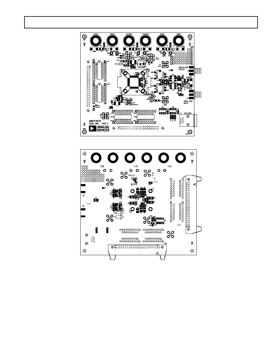
REV. 0
AD9777
≠45≠
Figure 63. AD9777 Evaluation Board Components, Top Side
Figure 64. AD9777 Evaluation Board Components, Bottom Side
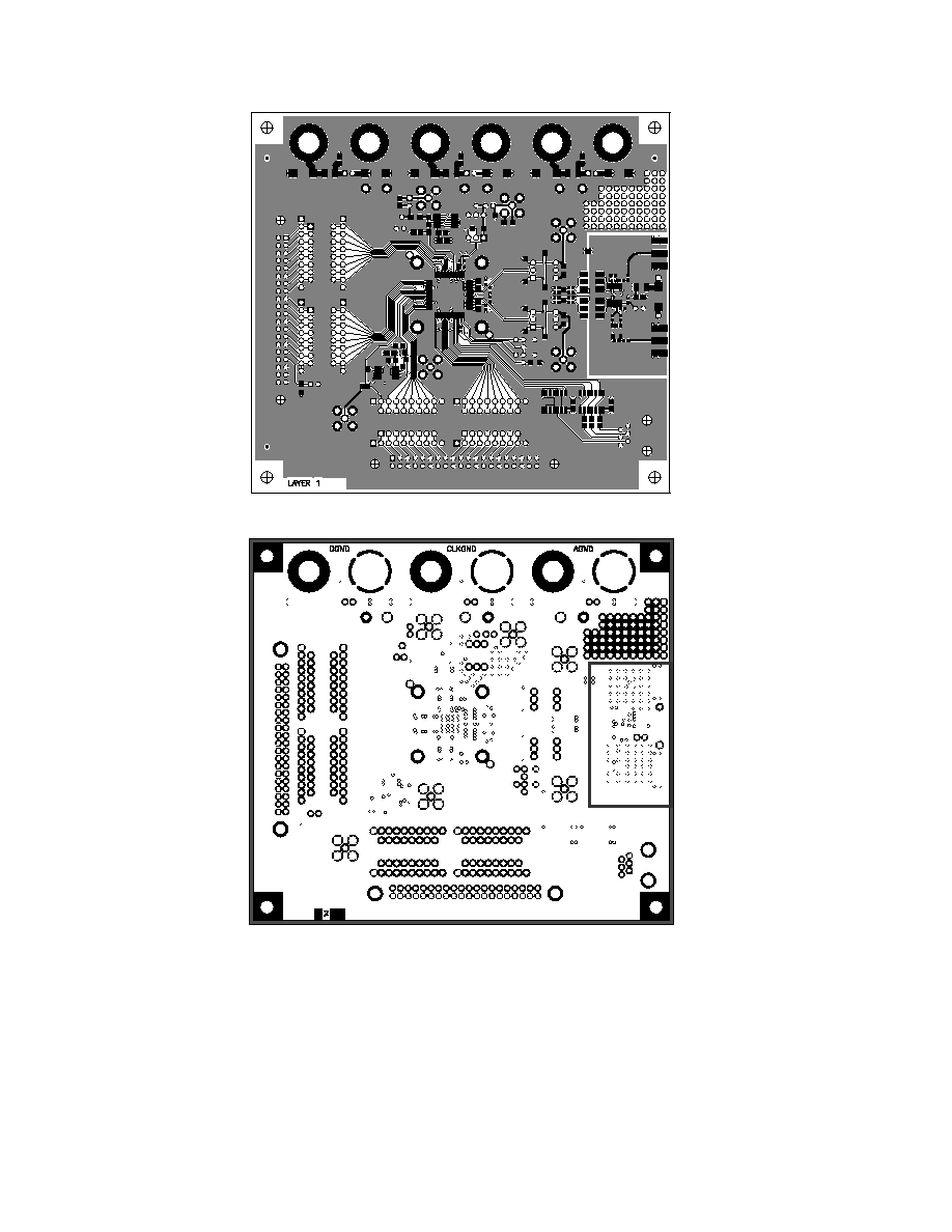
REV. 0
≠46≠
AD9777
Figure 65. AD9777 Evaluation Board Layout, Layer One (Top)
Figure 66. AD9777 Evaluation Board Layout, Layer Two (Ground Plane)

REV. 0
AD9777
≠47≠
Figure 67. AD9777 Evaluation Board Layout, Layer Three (Power Plane)
Figure 68. AD9777 Evaluation Board Layout, Layer Four (Bottom)
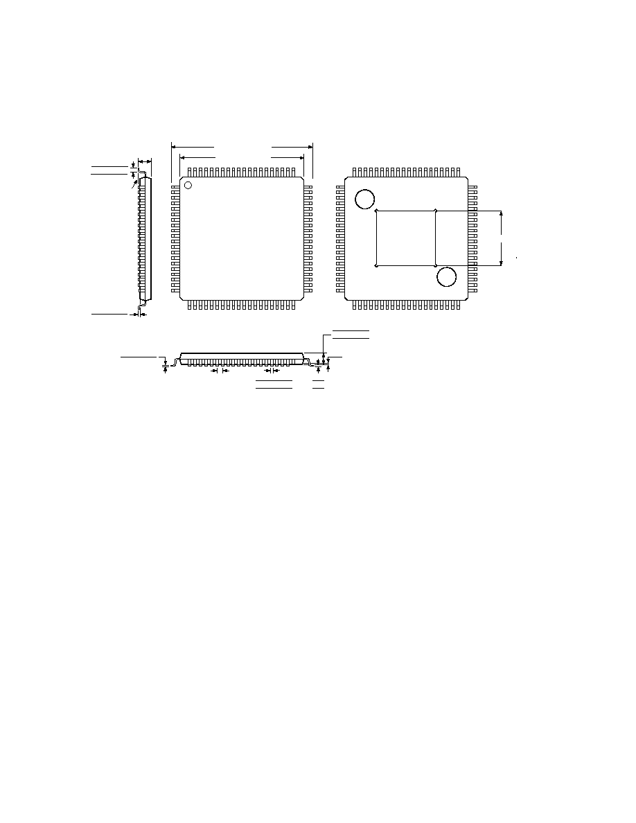
C02706≠0≠5/02(0)
PRINTED IN U.S.A.
≠48≠
AD9777
REV. 0
OUTLINE DIMENSIONS
80-Lead, Thermally Enhanced, Thin Plastic Quad Flatpack [TQFP]
(SV-80)
Dimensions shown in millimeters and (inches)
0.15 (0.0059)
0.05 (0.0020)
0.27 (0.0106)
0.22 (0.0087)
0.17 (0.0067)
0.20 (0.0079)
0.09 (0.0035)
0.50 (0.0197)
BSC
GAGE PLANE
0.25 (0.0098)
7
3.5
0
1.05 (0.0413)
1.00 (0.0394)
0.95 (0.0374)
1
20
21
41
40
60
80
61
PIN 1
TOP VIEW
(PINS
DOWN)
14.00 (0.5512) SQ
12.00 (0.4724) SQ
SEATING
PLANE
1.20 (0.0472)
MAX
0.75 (0.0295)
0.60 (0.0236)
0.45 (0.0177)
1
20
21
41
40
60
80
61
6.00 (0.2362) SQ
BOTTOM
VIEW
COPLANARITY
CONTROLLING DIMENSIONS ARE IN MILLIMETERS; INCH DIMENSIONS
(IN PARENTHESES) ARE ROUNDED-OFF MILLIMETER EQUIVALENTS FOR
REFERENCE ONLY AND ARE NOT APPROPRIATE FOR USE IN DESIGN
COMPLIANT TO JEDEC STANDARDS MO-026-ADD
AN APPLICATION NOTE DETAILING THE THERMALLY ENHANCED TQFP
CAN BE FOUN
D AT;
www.amkor.com/products/notes_papers/MLF_Appnote_0301.pdf