 | –≠–ª–µ–∫—Ç—Ä–æ–Ω–Ω—ã–π –∫–æ–º–ø–æ–Ω–µ–Ω—Ç: AD9779 | –°–∫–∞—á–∞—Ç—å:  PDF PDF  ZIP ZIP |
Rev. PrD
Information furnished by Analog Devices is believed to be accurate and reliable.
However, no responsibility is assumed by Analog Devices for its use, nor for any
infringements of patents or other rights of third parties that may result from its use.
Specifications subject to change without notice. No license is granted by implication
or otherwise under any patent or patent rights of Analog Devices. Trademarks and
registered trademarks are the property of their respective owners.
One Technology Way, P.O. Box 9106, Norwood, MA 02062-9106, U.S.A.
Tel: 781.329.4700
www.analog.com
Fax: 781.326.8703
© 2005 Analog Devices, Inc. All rights reserved.
Dual 16-Bit, 1.0 GSPS
D/A Converter
Preliminary Technical Data
AD9779
FEATURES
∑
1.8/3.3 V Single Supply Operation
∑
Low power: 950mW (I
OUTFS
= 20 mA; f
DAC
= 1 GSPS, 4
◊
Interpolation
∑
DNL = ± 1.5 LSB, INL = ± 5.0 LSB
∑
SFDR =82 dBc to f
OUT
= 100 MHz
∑
ACLR = 87 dBc @ 80 MHz IF
∑
CMOS data interface with Autotracking Input Timing
∑
Analog Output: Adjustable 10-30mA (RL=25
to 50 )
∑
100-lead Exposed Paddle TQFP Package
∑
Multiple Chip Synchronization Interface
∑
84dB Digital Interpolation Filter Stopband Attenuation
∑
Digital Inverse Sinc Filter
APPLICATIONS
∑
Wireless Infrastructure
Direct Conversion
Transmit Diversity
∑
Wideband Communications Systems:
Point-to-Point Wireless, LMDS
PRODUCT DESCRIPTION
The AD9779 is a dual 16-bit high performance, high frequency
DAC that provides a sample rate of 1 GSPS, permitting multi
carrier generation up to its Nyquist frequency. It includes features
optimized for direct conversion transmit applications, including
complex digital modulation and gain and offset compensation. The
DAC outputs are optimized to interface seamlessly with analog
quadrature modulators such as the AD8349. A serial peripheral
interface (SPI) provides for programming many internal
parameters and also enables read-back of status registers. The
output current can be programmed over a range of 10mA to 30mA.
The AD9779 is manufactured on an advanced 0.18µm CMOS
process and operates from 1.8V and 3.3V supplies for a total power
consumption of 950mW. It is supplied in a 100-lead QFP package.
PRODUCT HIGHLIGHTS
Ultra-low noise and Intermodulation Distortion (IMD) enable
high quality synthesis of wideband signals from baseband to high
intermediate frequencies.
Single-ended CMOS interface supports a maximum input rate of
300 MSPS with 1x interpolation.
Manufactured on a CMOS process, the AD9779 uses a proprietary
switching technique that enhances dynamic performance.
The current outputs of the AD9779 can be easily configured for
various single-ended or differential circuit topologies.
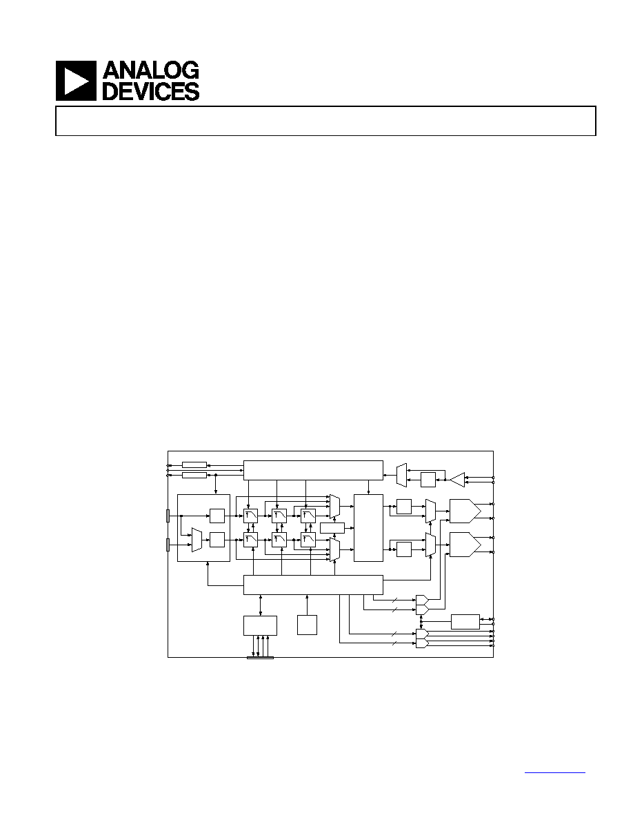
FUNCTIONAL BLOCK DIAGRAM
Complex
Modulator
Clock Generation/Distribution
2X
n * Fdac/8
n = 1, 2, 3... 7
P2D[15:0]
IOUT2_P
IOUT2_N
CLK+
CLK-
DATACLK_OUT
2X
2X
2X
2X
2X
Sinc
-1
Sinc
-1
16-Bit
IDAC
16-Bit
QDAC
Digital Controller
Clock
Multiplier
2X/4X/8X
Gain
Gain
Offset
Offset
Reference
& Bias
10
10
10
10
Power-On
Reset
Serial
Peripheral
Interface
Q Latch
I Latch
Delay Line
Delay Line
Data
Assembler
SDI
O
SD
O
SC
L
K
CSB
IOUT1_P
IOUT1_N
VREF
RSET
AUX1_P
AUX1_N
AUX2_P
AUX2_N
P1D[15:0]
SYNC_I
SYNC_O
Figure 1 Functional Block Diagram

AD9779
Preliminary Technical Data
Rev. PrD | Page 2 of 34
TABLE OF CONTENTS
Specifications............................................................................................3
DC SPECIFICATIONS ......................................................................3
DIGITAL SPECIFICATIONS............................................................4
AC SPECIFICATIONS.......................................................................4
Pin Function Descriptions .....................................................................5
Pin Configuration....................................................................................6
Interpolation Filter Coefficients............................................................7
INTERPOLATION Filter RESPONSE CURVES ................................8
CHARACTERIZATION DATA ............................................................9
General Description ..............................................................................12
Serial Peripheral Interface................................................................12
General Operation of the Serial Interface......................................12
Instruction Byte .................................................................................12
Serial Interface Port Pin Descriptions ............................................12
MSB/LSB Transfers ...........................................................................13
Notes on Serial Port Operation .......................................................13
SPI Register Map ...............................................................................14
Internal Reference/Full Scale Current Generation .......................22
Auxiliary DACs..................................................................................22
Power Down and Sleep Modes ........................................................22
Internal PLL Clock Multiplier / Clock Distribution.....................23
Timing Information ..........................................................................23
Interpolation Filter Architecture.....................................................25
EvaLuation Board Schematics..............................................................27
REVISION HISTORY
Revision PrA: Initial Version
Revision PrB: Updated Page 1 Features, added eval board schematics, SPI register map, filter coefficients and filter response curves
Revision PrC: Added characterization data, description of modulation modes, internal clock distribution architecture, timing information
Revision PrD: Added more ac characterization data, power dissipation
Preliminary Technical Data
AD9779
Rev. PrD | Page 3 of 34
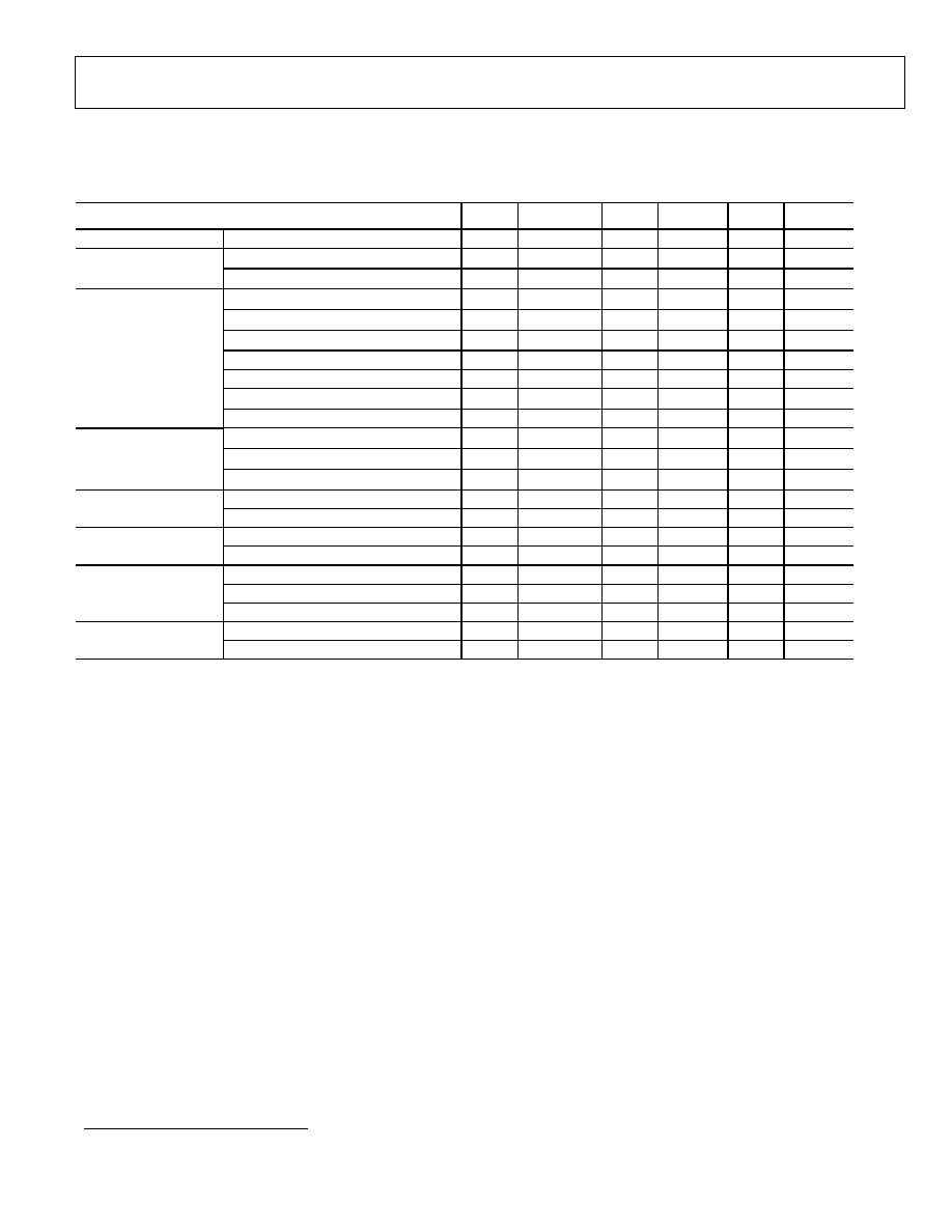
SPECIFICATIONS
1
DC SPECIFICATIONS
(VDD33 = 3.3 V, VDD18 = 1.8 V, MAXIMUM SAMPLE RATE, UNLESS OTHERWISE NOTED)
Parameter Temp
Test
Level
Min
Typ
Max
Unit
RESOLUTION
16
Bits
Integral Nonlinearity (DNL)
± 1.5
LSB
ACCURACY
Differential Nonlinearity (INL)
± 5
LSB
Offset Error
± TBD
%
FSR
Gain Error (With Internal Reference)
± TBD
%
FSR
Gain Error (Without Internal Reference)
± TBD
%
FSR
Full Scale Output Current
10
20
30
mA
Output Compliance Range
1.0
V
Output Resistance
TBD
k
ANALOG OUTPUTS
Output Capacitance
TBD
pF
Offset
TBD
ppm/
∞C
Gain
TBD
ppm/
∞C
TEMPERATURE DRIFT
Reference Voltage
TBD
ppm/
∞C
Internal Reference Voltage
1.2
V
REFERENCE
Output Current
100
nA
VDDA33
3.13
3.3
3.47
V
ANALOG SUPPLY
VOLTAGES
VDDA18
1.70
1.8
1.90
V
VDDD33
3.13
3.3
3.47
V
VDDD18
1.70
1.8
1.90
V
DIGITAL SUPPLY
VOLTAGES
VDDCLK
1.70
1.8
1.90
V
600 MSPS
TBD
mW
POWER CONSUMPTION
Standby Power
TBD
mW
Table 1: DC Specifications
1
Specifications subject to change without notice
AD9779
Preliminary Technical Data
Rev. PrD | Page 4 of 34
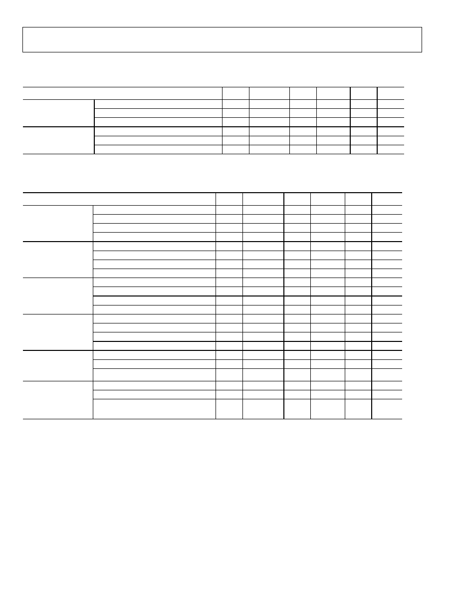
DIGITAL SPECIFICATIONS
(VDD33 = 3.3 V, VDD18 = 1.8 V, MAXIMUM SAMPLE RATE, UNLESS OTHERWISE NOTED)
Parameter Temp
Test
Level
Min
Typ
Max
Unit
Differential peak-to-peak Voltage
800
mV
Common Mode Voltage
400
mV
DAC CLOCK INPUT
(CLK+, CLK-)
Maximum Clock Rate
1
GSPS
Maximum Clock Rate (SCLK)
40
MHz
Maximum Pulse width high
TBD
ns
SERIAL PERIPHERAL
INTERFACE
Maximum pulse width low
TBD
ns
Table 2: Digital Specifications
AC SPECIFICATIONS
(VDD33 = 3.3 V, VDD18 = 1.8 V, MAXIMUM SAMPLE RATE, UNLESS OTHERWISE NOTED)
Parameter Temp
Test
Level
Min
Typ
Max
Unit
Output Settling Time (tst) (to 0.025%)
TBD
ns
Output Rise Time (10% to 90%)
TBD
ns
Output Fall Time (90% to 10%)
TBD
ns
DYNAMIC
PERFORMANCE
Output Noise (IoutFS=20mA)
TBD
pA/rtHz
f
DAC
= 100 MSPS, f
OUT
= 20 MHz
82
dBc
f
DAC
= 200 MSPS, f
OUT
= 50 MHz
82
dBc
f
DAC
= 400 MSPS, f
OUT
= 70 MHz
84
dBc
SPURIOUS FREE
DYNAMIC RANGE
(SFDR)
f
DAC
= 800 MSPS, f
OUT
= 70 MHz
87
dBc
f
DAC
= 200 MSPS, f
OUT
= 50 MHz
91
dBc
f
DAC
= 400 MSPS, f
OUT
= 60 MHz
88
dBc
f
DAC
= 400 MSPS, f
OUT
= 80 MHz
81
dBc
TWO-TONE
INTERMODULATION
DISTORTION (IMD)
f
DAC
= 800 MSPS, f
OUT
= 100 MHz
88
dBc
f
DAC
= 156 MSPS, f
OUT
= 60 MHz
-158
dBm/Hz
f
DAC
= 200 MSPS, f
OUT
= 80 MHz
-157
dBm/Hz
f
DAC
= 312 MSPS, f
OUT
= 100 MHz
-159
dBm/Hz
NOISE SPECTRAL
DENSITY (NSD)
f
DAC
= 400 MSPS, f
OUT
= 100 MHz
-159
dBm/Hz
f
DAC
= 245.76 MSPS, f
OUT
= 20 MHz
80
dBc
f
DAC
= 491.52 MSPS, f
OUT
= 100 MHz
79
dBc
WCDMA ADJACENT
CHANNEL LEAKAGE
RATIO (ACLR), SINGLE
CARRIER
f
DAC
= 491.52 MSPS, f
OUT
= 200 MHz
74
dBc
f
DAC
= 245.76 MSPS, f
OUT
= 60 MHz
78
dBc
f
DAC
= 491.52 MSPS, f
OUT
= 100 MHz
80
dBc
WCDMA SECOND
ADJACENT CHANNEL
LEAKAGE RATIO
(ACLR), SINGLE
CARRIER
f
DAC
= 491.52 MSPS, f
OUT
= 200 MHz
76
dBc
Table 3: AC Specifications
Preliminary Technical Data
AD9779
Rev. PrD | Page 5 of 34
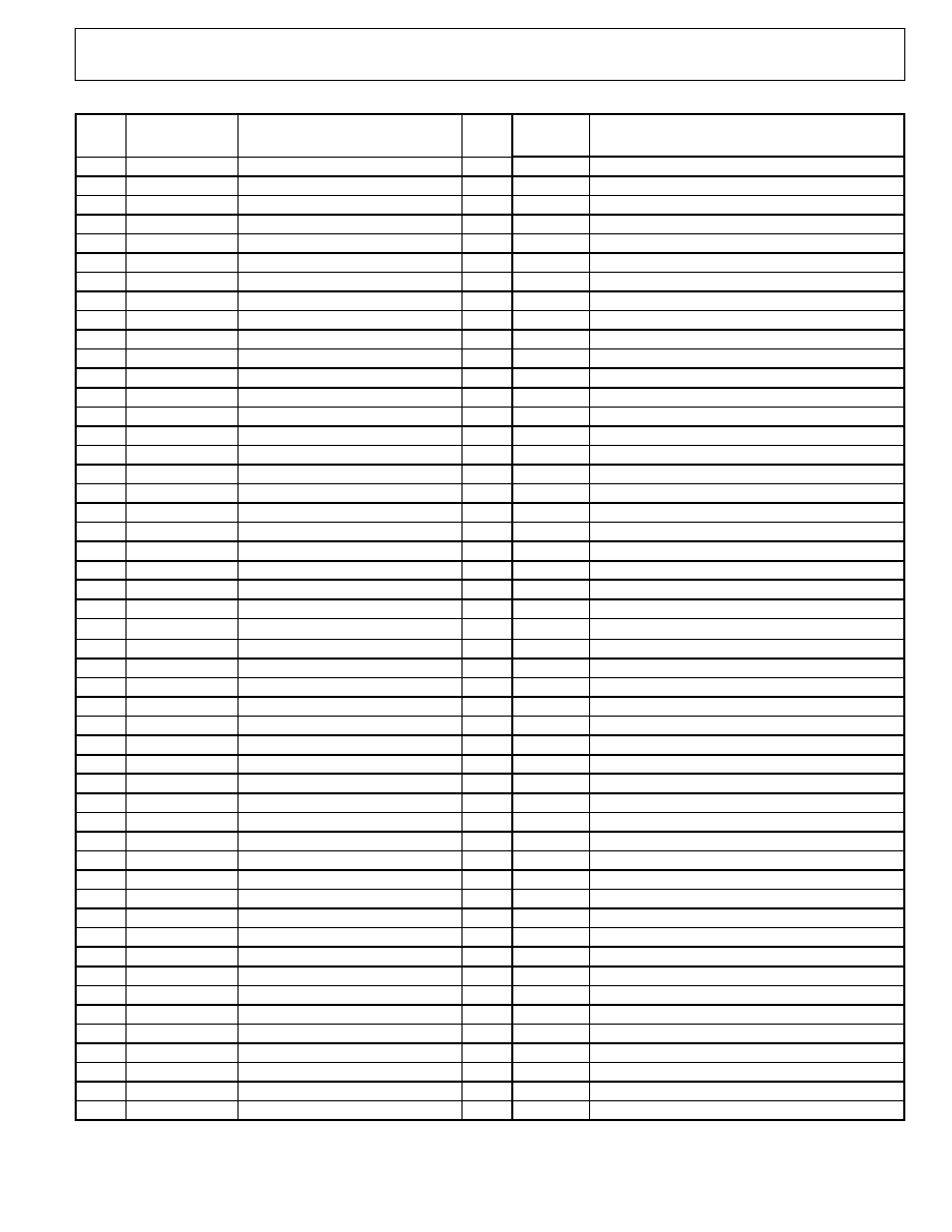
PIN FUNCTION DESCRIPTIONS
Pin
No.
Name Description
Pin
No.
Name Description
1
VDDC18
1.8 V Clock Supply
51
P2D<6>
Port 2 Data Input D6
2
VDDC18
1.8 V Clock Supply
52
P2D<5>
Port 2 Data Input D5
3
VSSC
Clock Common
53
VDDD18
1.8 V Digital Supply
4
VSSC
Clock Common
54
VSSD
Digital Common
5
CLK+
Differential Clock Input
55
P1D<4>
Port 2 Data Input D4
6
CLK-
Differential Clock Input
56
P1D<3>
Port 2 Data Input D3
7
VSSC
Clock Common
57
P1D<2>
Port 2 Data Input D2
8
VSSC
Clock Common
58
P1D<1>
Port 2 Data Input D1
9
VDDC18
1.8 V Clock Supply
59
P1D<0>
Port 2 Data Input D0 (LSB)
10
VDDC18
1.8 V Clock Supply
60
VDDD18
1.8 V Digital Supply
11
VSSC
Clock Common
61
VDDD33
3.3 V Digital Supply
12 VSSC
Clock
Common
62
SYNC_O-
Differential Synchronization Output
13
SYNC_I+
Differential Synchronization Input
63
SYNC_O+ Differential
Synchronization
Output
14 SYNC_I-
Differential
Synchronization Input
64
VSSD
Digital Common
15
VSSD
Digital Common
65
PLL_LOCK
PLL Lock Indicator
16
VDDD33
3.3 V Digital Supply
66
SPI_SDO
SPI Port Data Output
17
P1D<15>
Port 1 Data Input D15 (MSB)
67
SPI_SDIO
SPI Port Data Input/Output
18
P1D<14>
Port 1 Data Input D14
68
SPI_CLK
SPI Port Clock
19
P1D<13>
Port 1 Data Input D13
69
SPI_CSB
SPI Port Chip Select Bar
20
P1D<12>
Port 1 Data Input D12
70
RESET
Reset
21
P1D<11>
Port 1 Data Input D11 71
IRQ
Interrupt
Request
22
VSSD
Digital Common
72
VSS
Analog Common
23
VDDD18
1.8 V Digital Supply
73
IPTAT
Reference Current
24
P1D<10>
Port 1 Data Input D10
74
VREF
Voltage Reference Output
25
P1D<9>
Port 1 Data Input D9
75
I120
120
µA Reference Current
26
P1D<8>
Port 1 Data Input D8
76
VDDA33
3.3 V Analog Supply
27
P1D<7>
Port 1 Data Input D7
77
VSSA
Analog Common
28
P1D<6>
Port 1 Data Input D6
78
VDDA33
3.3 V Analog Supply
29
P1D<5>
Port 1 Data Input D5
79
VSSA
Analog Common
30
P1D<4>
Port 1 Data Input D4
80
VDDA33
3.3 V Analog Supply
31
P1D<3>
Port 1 Data Input D3
81
VSSA
Analog Common
32
VSSD
Digital Common
82
VSSA
Analog Common
33
VDDD18
1.8 V Digital Supply
83
IOUT2_P
Differential DAC Current Output, Channel 2
34
P1D<2>
Port 1 Data Input D2
84
IOUT2_N
Differential DAC Current Output, Channel 2
35
P1D<1>
Port 1 Data Input D1
85
VSSA
Analog Common
36
P1D<0>
Port 1 Data Input D0 (LSB)
86
AUX2_P
Auxiliary DAC Voltage Output, Channel 2
37
DATACLK_OUT
Data Clock Output
87
AUX2_N
Auxiliary DAC Voltage Output, Channel 2
38
VDDD33
3.3 V Digital Supply
88
VSSA
Analog Common
39 TXENABLE
Transmit
Enable
89
AUX1_N
Auxiliary DAC Voltage Output, Channel 1
40
P2D<15>
Port 2 Data Input D15 (MSB)
90
AUX1_P
Auxiliary DAC Voltage Output, Channel 1
41
P2D<14>
Port 2 Data Input D14
91
VSSA
Analog Common
42
P2D<13>
Port 2 Data Input D13
92
IOUT1_N
Differential DAC Current Output, Channel 1
43
VDDD18
1.8 V Digital Supply
93
IOUT1_P
Differential DAC Current Output, Channel 1
44
VSSD
Digital Common
94
VSSA
Analog Common
45
P2D<12>
Port 2 Data Input D12
95
VSSA
Analog Common
46
P2D<11>
Port 2 Data Input D11
96
VDDA33
3.3 V Analog Supply
47
P2D<10>
Port 2 Data Input D10
97
VSSA
Analog Common
48
P2D<9>
Port 2 Data Input D9
98
VDDA33
3.3 V Analog Supply
49
P2D<8>
Port 2 Data Input D8
99
VSSA
Analog Common
50
P2D<7>
Port 2 Data Input D7
100
VDDA33
3.3 V Analog Supply
Table 4: Pin Function Descriptions
AD9779
Preliminary Technical Data
Rev. PrD | Page 6 of 34
PIN CONFIGURATION
VDDD18
VDDD18
VSSD
P2D<5>
P2D<4>
P2D<3>
P2D<2>
P2D<1>
P2D<0>
SYNC_O-
SPI_SDO
SPI_SDI
51
52
53
54
VDD
A
33
VS
SA
VDD
A
33
VS
SA
VDD
A
33
VS
SA
AU
X
2
_P
AUX
2
_N
VS
SA
IO
U
T
2_
P
IO
UT
2
_
N
VS
SA
VS
SA
VS
SA
IO
UT
1
_
N
IO
U
T
1_
P
VS
SA
AUX
1
_N
76
77
78
79
VSSD
VDDD33
VSSD
VDDD18
P1D<10>
P1D<11>
P1D<12>
P1D<13>
P1D<14>
P1D<15>
SYNC_I-
SYNC_I+
VSSC
VSSC
P2D
<
1
1
>
VD
D
D
33
P2D
<
1
2
>
P2D
<
1
3
>
P2D
<
1
4
>
P2D
<
1
5
>
DC
LK
P1D
<
0>
P1D
<
1>
P1D
<
2>
P1D
<
3>
VD
D
D
18
VS
SD
P1D
<
4>
P1D
<
5>
P1D
<
6>
P1D
<
7>
P1D
<
8>
P1D<9>
27
26
P2D
<
7>
P2D
<
8>
P2D
<
9>
P2D
<
1
0
>
50
49
AU
X
1
_P
VS
SA
VDD
A
33
VS
SA
VDD
A
33
CLK-
CLK+
VDDC18
VSSC
VSSC
3
2
VDDC18
VSSC
VSSC
VDDC18
1
VDDC18
25
24
75
74
100
99
SPI_CLK
SPI_CSB
RESET
IPTAT
VREF
IRQ
AD9779
VS
SA
VDD
A
33
SYNC_O+
VSSD
VSS
TXE
n
a
b
le
P2D<6>
73
72
71
70
69
68
67
66
65
64
63
62
61
60
59
58
57
56
55
6
5
4
9
8
7
12
11
10
15
14
13
18
17
16
21
20
19
23
22
34
33
30
29
28
32
31
36
35
43
42
39
38
37
41
40
48
47
44
46
45
80
81
84
82
83
85
86
89
87
88
90
91
94
92
93
95
98
96
97
I120
PLL_LOCK
Analog Domain
Digital Domain
VD
D
D
18
VS
SD
VDDD33
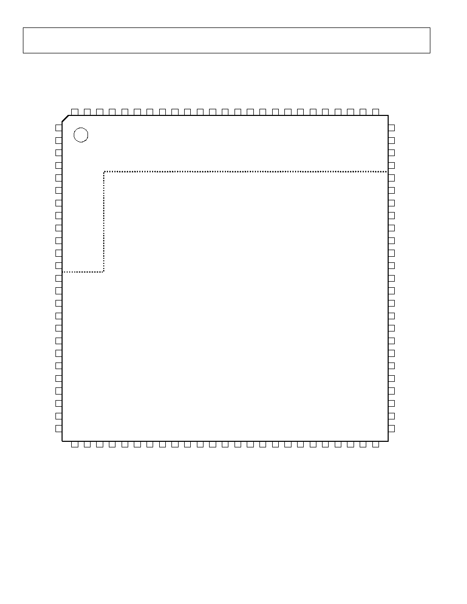
Figure 2. Pin Configuration
Preliminary Technical Data
AD9779
Rev. PrD | Page 7 of 34
INTERPOLATION FILTER COEFFICIENTS
Table 5: Halfband Filter 1
Lower
Coefficient
Upper
Coefficient
Integer
Value
H(1) H(55) -4
H(2) H(54) 0
H(3) H(53) 13
H(4) H(52) 0
H(5) H(51) -34
H(6) H(50) 0
H(7) H(49) 72
H(8) H(48) 0
H(9) H(47) -138
H(10) H(46) 0
H(11) H(45) 245
H(12) H(44) 0
H(13) H(43) -408
H(14) H(42) 0
H(15) H(41) 650
H(16) H(40) 0
H(17) H(39) -1003
H(18) H(38) 0
H(19) H(37) 1521
H(20) H(36) 0
H(21) H(35) -2315
H(22) H(34) 0
H(23) H(33) 3671
H(24) H(32) 0
H(25) H(31) -6642
H(26) H(30) 0
H(27) H(29) 20755
H(28)
32768
Table 6: Halfband Filter 2
Lower
Coefficient
Upper
Coefficient
Integer
Value
H(1) H(23) -2
H(2) H(22) 0
H(3) H(21) 17
H(4) H(20) 0
H(5) H(19) -75
H(6) H(18) 0
H(7) H(17) 238
H(8) H(16) 0
H(9) H(15) -660
H(10) H(14) 0
H(11) H(13) 2530
H(12)
4096
Table 7: Halfband Filter 3
Lower
Coefficient
Upper
Coefficient
Integer
Value
H(1) H(15) -39
H(2) H(14) 0
H(3) H(13) 273
H(4) H(12) 0
H(5) H(11) -1102
H(6) H(10) 0
H(7) H(9) 4964
H(8)
8192
Table 8: Inverse Sinc Filter
Lower
Coefficient
Upper
Coefficient
Integer
Value
H(1) H(9) 2
H(2) H(8) -4
H(3) H(7) 10
H(4) H(6) -35
H(5)
401
AD9779
Preliminary Technical Data
Rev. PrD | Page 8 of 34
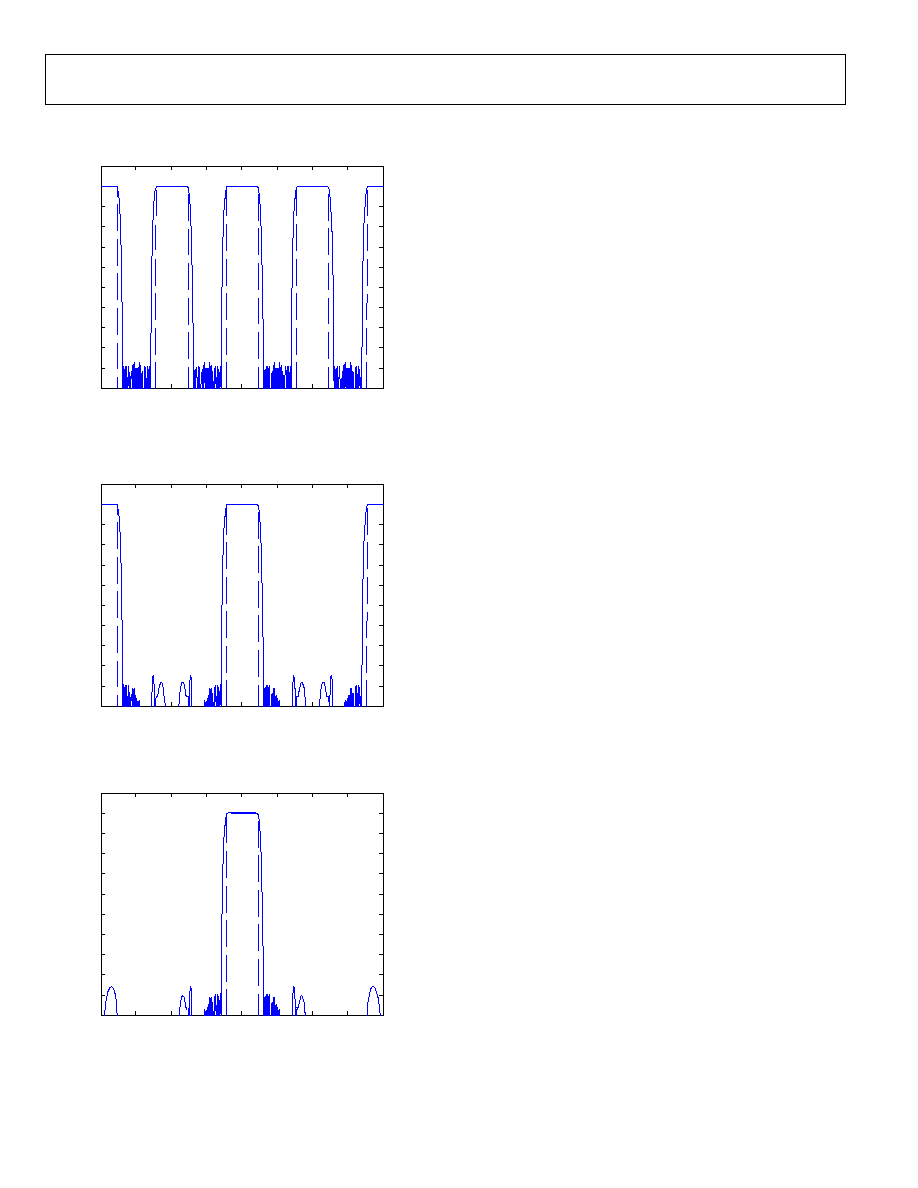
INTERPOLATION FILTER RESPONSE CURVES
-4
-3
-2
-1
0
1
2
3
4
-100
-90
-80
-70
-60
-50
-40
-30
-20
-10
0
10
Figure 3. AD9779 2x Interpolation, Low Pass Response to
±4x Input Data Rate (Dotted Lines Indicate 1dBRoll-Off)
-4
-3
-2
-1
0
1
2
3
4
-100
-90
-80
-70
-60
-50
-40
-30
-20
-10
0
10
Figure 4. AD9779 4x Interpolation, Low Pass Response to
±4x Input Data Rate (Dotted Lines Indicate 1dBRoll-Off)
-4
-3
-2
-1
0
1
2
3
4
-100
-90
-80
-70
-60
-50
-40
-30
-20
-10
0
10
Figure 5.AD9779 8x Interpolation, Low Pass Response to
±4x Input Data Rate (Dotted Lines Indicate 1dBRoll-Off)

Preliminary Technical Data
AD9779
Rev. PrD | Page 9 of 34
CHARACTERIZATION DATA
-5
-4
-3
-2
-1
0
1
2
3
4
5
6
0
8192
16384
24576
32768
40960
49152
57344
65536
Code
IN
L
(L
S
B
s
)
Figure 6. AD9779 Typical INL
-1
-0.5
0
0.5
1
1.5
2
0
8192
16384
24576
32768
40960
49152
57344
65536
Code
DNL
(
L
SBs
)
Figure 7. AD9779 Typical DNL
50
60
70
80
90
100
0
20
40
60
80
100
Fout - MHz
S
F
DR -
d
B
m
F
D ATA
=100MSPS
F
D ATA
=160MSPS
F
D ATA
=200MSPS
Figure 8. SFDR vs. F
OUT
, 1x Interpolation
50
55
60
65
70
75
80
85
90
95
100
0
20
40
60
80
100
Fout - MHz
S
F
DR -
d
B
m
F
DATA
=100MSPS
F
DATA
=160MSPS
F
DATA
=200MSPS
Figure 9. SFDR vs. F
OUT
, 2x Interpolation
50
55
60
65
70
75
80
85
90
95
100
0
20
40
60
80
Fout - MHz
SF
D
R
-
d
B
m
F
D ATA
=100MSPS
F
D ATA
=125MSPS
F
D ATA
=150MSPS
F
D ATA
=200MSPS
Figure 10. SFDR vs. F
OUT
, 4x Interpolation
50
60
70
80
90
100
0
10
20
30
40
50
Fout - M Hz
S
F
DR -
d
B
m
50MSPS
75MSPS
F
D ATA
=62.5MSPS
100MSPS
Figure 11. SFDR vs. F
OUT
, 8x Interpolation

AD9779
Preliminary Technical Data
Rev. PrD | Page 10 of 34
50.0
60.0
70.0
80.0
90.0
100.0
0
20
40
60
80
Fout - MHz
IM
D
-
dB
c
F
DATA
=160MSPS
F
D ATA
=200MSPS
Figure 12. Third Order IMD vs. F
OUT
, 1x Interpolation
50.0
60.0
70.0
80.0
90.0
100.0
0
20
40
60
80
100
120
140
160
180
200
Fout - MHz
IM
D
-
d
B
c
F
D ATA
=160MSPS
F
D ATA
=200MSPS
Figure 13. Third Order IMD vs. F
OUT
, 2x Interpolation
50
60
70
80
90
100
0
40
80
120
160
200
240
280
320
360
400
Fout - MHz
IM
D
- d
B
c
F
D ATA
=100MSPS
F
D ATA
=125MSPS
F
D ATA
=150MSPS
F
D ATA
=200MSPS
Figure 14. Third Order IMD vs. F
OUT
, 4x Interpolation
50
60
70
80
90
100
0
50
100
150
200
250
300
350
400
450
Fout - MHz
IM
D
-
d
B
c
50MSPS
100MSPS
F
D ATA
=62.5MSPS
112.5MSPS
75MSPS
Figure 15. Third Order IMD vs. F
OUT
, 8x Interpolation
-170
-168
-166
-164
-162
-160
-158
-156
-154
-152
-150
0
10
20
30
40
50
60
70
80
90
Fout - M Hz
NS
D -
d
B
m
/
Hz
F
D ATA
=78MSPS
F
D ATA
=156MSPS
F
D ATA
=200MSPS
Figure 16. Noise Spectral Density vs. F
OUT
, 1x Interpolation
-170
-168
-166
-164
-162
-160
-158
-156
-154
-152
-150
0
20
40
60
80
100
120
140
160
180
Fout - MHz
NS
D
-
d
B
m
/
Hz
F
D ATA
=78MSPS
F
D ATA
=156MSPS
F
DATA
=200MSPS
Figure 17. Noise Spectral Density vs. F
OUT
, 2x Interpolation

Preliminary Technical Data
AD9779
Rev. PrD | Page 11 of 34
-90
-85
-80
-75
-70
-65
-60
-55
-50
0
20
40
60
80
100 120 140 160 180 200 220 240 260 280 300
Fout - MHz
ACL
R -
d
B
c
F
D ATA
=122.88MSPS
F
D ATA
=61.44MSPS
Figure 18. ACLR for 1
st
Adjacent Band WCDMA, 4x Interpolation. On-Chip
Modulation is used to translate baseband signal to IF.
-90
-85
-80
-75
-70
-65
-60
-55
-50
0
20
40
60
80 100 120 140 160 180 200 220 240 260 280 300
Fout - MHz
ACL
R
-
d
B
c
F
D ATA
=122.88MSPS
F
D ATA
=61.44MSPS
Figure 19. ACLR for 2nd Adjacent Band WCDMA, 4x Interpolation. On-Chip
Modulation is used to translate baseband signal to IF.
-90
-85
-80
-75
-70
-65
-60
-55
-50
0
20
40
60
80
100 120 140 160 180 200 220 240 260 280 300
Fout - MHz
ACL
R
-
d
B
c
F
D ATA
=122.88MSPS
F
DATA
=61.44MSPS
Figure 20. ACLR for 3rd Adjacent Band WCDMA, 4x Interpolation. On-Chip
Modulation is used to translate baseband signal to IF.
0
0.1
0.2
0.3
0.4
0.5
0.6
0.7
0
25
50
75
100
125
150
175
200
225
250
F
DATA
(MSPS)
Po
w
e
r
-
W
8x Interpolation,
Zero Stuffing
4x Interpolation,
Zero Stuffing
4x Interpolation
2x Interpolation,
Zero Stuffing
2x Interpolation
1x Interpolation,
Zero Stuffing
1x Interpolation
8x Interpolation
Figure 21. Power Dissipation, Single DAC Mode
0
0.1
0.2
0.3
0.4
0.5
0.6
0.7
0.8
0.9
1
1.1
0
25
50
75
100
125
150
175
200
225
250
F
DATA
(MSPS)
Pow
e
r
-
W
8x Interpolation,
Zero Stuffing
8x Interpolation,F
DA C
/4 Modulation
4x Interpolation,
Zero Stuffing
8x Interpolation,F
DA C
/2 Modulation
8x Interpolation,F
DA C
/8 Modulation
8x Interpolation,Modulation off
4x Interpolation,F
DA C
/4 Modulation
4x Interpolation,F
DA C
/2 Modulation
4x Interpolation,Modulation off
2x Interpolation,
Zero Stuffing
2x Interpolation,F
DA C
/2 Modulation
2x Interpolation,Modulation off
1x Interpolation,
Zero Stuffing
1x Interpolation
Figure 22. Power Dissipation, Dual DAC Mode
0
0.02
0.04
0.06
0.08
0.1
0.12
0.14
0.16
0
200
400
600
800
1000
1200
F
DAC
- M SPS
Po
w
e
r
-
W
Figure 23. Power Dissipation of Inverse Sinc Filter

AD9779
Preliminary Technical Data
Rev. PrD | Page 12 of 34
GENERAL DESCRIPTION
The AD9779 combines many features which make it make it a very
attractive DAC for wired and wireless communications systems.
The dual digital signal path and dual DAC structure allow an easy
interface with common quadrature modulators when designing
single sideband transmitters. The speed and performance of the
AD9779 allow wider bandwidths/more carriers to be synthesized
than with previously available DACs. The digital engine in the
AD9779 uses a breakthrough filter architecture that combines the
interpolation with a digital quadrature modulator. This allows the
AD9779 to do digital quadrature frequency up conversion. The
AD9779 also has features which allow simplified synchronization
with incoming data, and also allows multiple AD9779s to be
synchronized.
Serial Peripheral Interface
AD9779
SPI
PORT
SPI_CSB (pin 69)
SPI_SCLK (pin 68)
SPI_SDI (pin 67)
SPI_SDO (pin 66)
Figure 24. AD9779 SPI Port
The AD9779 serial port is a flexible, synchronous serial
communications port allowing easy interface to many industry-
standard microcontrollers and microprocessors. The serial I/O is
compatible with most synchronous transfer formats, including both
the Motorola SPIÆ and IntelÆ SSR protocols. The interface allows
read/write access to all registers that configure the AD9779. Single
or multiple byte transfers are supported, as well as MSB first or LSB
first transfer formats. The AD9779's serial interface port can be
configured as a single pin I/O (SDIO) or two unidirectional pins for
in/out (SDIO/SDO).
General Operation of the Serial Interface
There are two phases to a communication cycle with the AD9779.
Phase 1 is the instruction cycle, which is the writing of an
instruction byte into the AD9779, coincident with the first eight
SCLK rising edges. The instruction byte provides the AD9779 serial
port controller with information regarding the data transfer cycle,
which is Phase 2 of the communication cycle. The Phase 1
instruction byte defines whether the upcoming data transfer is read
or write, the number of bytes in the data transfer, and the starting
register address for the first byte of the data transfer. The first eight
SCLK rising edges of each communication cycle are used to write
the instruction byte into the AD9779.
A logic high on the CS pin, followed by a logic low, will reset the
SPI port timing to the initial state of the instruction cycle. This is
true regardless of the present state of the internal registers or the
other signal levels present at the inputs to the SPI port. If the SPI
port is in the midst of an instruction cycle or a data transfer
cycle,none of the present data will be written.
The remaining SCLK edges are for Phase 2 of the communication
cycle. Phase 2 is the actual data transfer between the AD9779 and
the system controller. Phase 2 of the communication cycle is a
transfer of 1, 2, 3, or 4 data bytes as determined by the instruction
byte. Using one multibyte transfer is the preferred method. Single
byte data transfers are useful to reduce CPU overhead when
register access requires one byte only. Registers change immediately
upon writing to the last bit of each transfer byte.
Instruction Byte
The instruction byte contains the information shown in Error!
Reference source not found.
.
MSB
LSB
I7 I6 I5 I4 I3 I2 I1 I0
R/W N1 N0 A4 A3 A2 A1 A0
Table 9. SPI Instruction Byte
R/W
, Bit 7 of the instruction byte, determines whether a read or a
write data transfer will occur after the instruction byte write. Logic
high indicates read operation. Logic 0 indicates a write operation.
N1, N0
, Bits 6 and 5 of the instruction byte, determine the number
of bytes to be transferred during the data transfer cycle. The bit
decodes are shown in Table 10.
A4, A3, A2, A1, A0
, Bits 4, 3, 2, 1, 0 of the instruction byte,
determine which register is accessed during the data transfer
portion of the communications cycle. For multibyte transfers, this
address is the starting byte address. The remaining register
addresses are generated by the AD9779 based on the LSBFIRST bit
(REG00, bit 6).
N1
N2
Description
0
0
Transfer 1 Byte
0
1
Transfer 2 Bytes
1
0
Transfer 3 Bytes
1
1
Transfer 4 Bytes
Table 10. Byte Transfer Count
Serial Interface Port Pin Descriptions
SCLK--Serial Clock
. The serial clock pin is used to synchronize
data to and from the AD9779 and to run the internal state
machines. SCLK's maximum frequency is 20 MHz. All data input
to the AD9779 is registered on the rising edge of SCLK. All data is
driven out of the AD9779 on the falling edge of SCLK.
CSB--Chip Select
. Active low input starts and gates a
communication cycle. It allows more than one device to be used on
the same serial communications lines. The SDO and SDIO pins will
go to a high impedance state when this input is high. Chip select
should stay low during the entire communication cycle.
SDIO--Serial Data I/O
. Data is always written into the AD9779 on
Preliminary Technical Data
AD9779
Rev. PrD | Page 13 of 34
this pin. However, this pin can be used as a bidirectional data line.
The configuration of this pin is controlled by Bit 7 of register
address 00h. The default is Logic 0, which configures the SDIO pin
as unidirectional.
SDO--Serial Data Out
. Data is read from this pin for protocols
that use separate lines for transmitting and receiving data. In the
case where the AD9779 operates in a single bidirectional I/O mode,
this pin does not output data and is set to a high impedance stat
e.
MSB/LSB Transfers
The AD9779 serial port can support both most significant bit
(MSB) first or least significant bit (LSB) first data formats. This
functionality is controlled by register bit LSBFIRST (REG00, bit 6).
The default is MSB first (LSBFIRST = 0).
When LSBFIRST = 0 (MSB first) the instruction and data bytes
must be written from most significant bit to least significant bit.
Multibyte data transfers in MSB first format start with an
instruction byte that includes the register address of the most
significant data byte. Subsequent data bytes should follow in order
from high address to low address. In MSB first mode, the serial
port internal byte address generator decrements for each data byte
of the multibyte communication cycle.
When LSBFIRST = 1 (LSB first) the instruction and data bytes
must be written from least significant bit to most significant bit.
Multibyte data transfers in LSB first format start with an
instruction byte that includes the register address of the least
significant data byte followed by multiple data bytes. The serial port
internal byte address generator increments for each byte of the
multibyte communication cycle.
The AD9779 serial port controller data address will decrement
from the data address written toward 0x00 for multibyte I/O
operations if the MSB first mode is active. The serial port controller
address will increment from the data address written toward 0x1F
for multibyte I/O operations if the LSB first mode is active.
Notes on Serial Port Operation
The AD9779 serial port configuration is controlled by REG00, bits
6 and 7 . It is important to note that the configuration changes
immediately upon writing to the last bit of the register. For
multibyte transfers, writing to this register may occur during the
middle of communication cycle. Care must be taken to compensate
for this new configuration for the remaining bytes of the current
communication cycle.
The same considerations apply to setting the software reset, RESET
(REG00, bit 5). All registers are set to their default values EXCEPT
REG00 and REG04 which remain unchanged.
Use of only single byte transfers when changing serial port
configurations or initiating a software reset is recommended to
prevent unexpected device behavior.
R/W N0 N1 A0 A1
A2 A3 A4 D7 D6
N
D5
N
D0
0
D1
0
D2
0
D3
0
D7 D6
N
D5
N
D0
0
D1
0
D2
0
D3
0
INSTRUCTION CYCLE
DATA TRANSFER CYCLE
CSB
SCLK
SDIO
SDO
03152-0-004
Figure 25. Serial Register Interface Timing MSB First
A0 A1 A2 A3 A4
N1 N0 R/W D0
0
D1
0
D2
0
D7
N
D6
N
D5
N
D4
N
D0
0
D1
0
D2
0
D7
N
D6
N
D5
N
D4
N
INSTRUCTION CYCLE
DATA TRANSFER CYCLE
CSB
SCLK
SDIO
SDO
03152-0-005
Figure 26. Serial Register Interface Timing LSB First
INSTRUCTION BIT 6
INSTRUCTION BIT 7
CSB
SCLK
SDIO
t
DS
t
DS
t
DH
t
PWH
t
PWL
t
SCLK
03152-P
r
D-006
Figure 27. Timing Diagram for SPI Register Write
DATA BIT n≠1
DATA BIT n
CSB
SCLK
SDIO
SDO
03152-P
r
D-007
t
DV
Figure 28. Timing Diagram for SPI Register Read

AD9779
Preliminary Technical Data
Rev. PrD | Page 14 of 34
SPI Register Map
Register
Name
Address
Bit 7
Bit 6
Bit 5
Bit 4
Bit 3
Bit 2
Bit 1
Bit 0
Default
Comm
Register
00h 00 SDIO
Bidirectional
LSB,MSB First
Software
Reset
Power
Down
Mode
Auto
Power
Down
Enable
PLL Lock
Indicator
00h
01h
01
Filter Interpolation Factor
<1: 0>
Filter Interpolation Mode <4:0>
Zero
Stuffing
Enable
00h
Digital
Control
Register
02h
02
Data Format
One Port
Mode
Real Mode
Inverse
Sinc
Enable
DATACLK
Invert
IQ Select
Invert
Q First
00h
03h
03
Data Delay Mode <1:0>
Data Clock Delay <2:0>
Data Window Delay <2:0>
00h
04h
04
Sync Out Delay <3:0>
Sync Window Delay <3:0>
00h
Sync
Control
05h 05 Sync
Enable
Sync Driver
Enable
Dac Clock Offset <2:0>
00h
Interrupt
Register
06h 06 Data
Delay
IRQ
Sync Delay
IRQ
Cross
Control IRQ
Data
Delay
IRQ Enable
Sync Delay
IRQ Enable
Cross
Control IRQ
Enable
00h
07h
07
PLL Band Select <4:0>
PLL Loop Cap Select <2:0>
CFh
PLL Control
08h
08
PLL Enable
PLL Output Freq Divide
<1:0>
PLL Loop Freq Divide
<1:0>
PLL Loop Filter Pole/Zero <2:0>
37h
Misc.
Control
Register
09h 24 PLL
Error
Source
PLL Ref
Bypass
PLL Gain <2:0>
PLL Bias <2:0>
38h
0Ah
09
IDAC Gain Adjustment <7:0>
F9h
I DAC
Control
Register
0Bh
10
IDAC SLEEP
IDAC Power
Down
IDAC
Gain
Adjustment
<9:8>
01h
0Ch
11
Auxiliary DAC1 Data <7:0>
00h
Aux 1 DAC
Control
Register
0Dh 12 Auxiliary
DAC1 Sign
Auxiliary
DAC1
Current
Direction
Auxiliary
DAC1 Sleep
Auxiliary DAC1 Data
<9:8>
00h
0Eh
13
QDAC Gain Adjustment <7;0>
F9h
Q DAC
Control
Register
0Fh
14
QDAC SLEEP
QDAC Sleep
QDAC Gain Adjustment
<9:8>
01h

Preliminary Technical Data
AD9779
Rev. PrD | Page 15 of 34
10h
15
Auxiliary DAC2 Data <7:0>
00h
Aux 2 DAC
Control
Register
11h 16 Auxiliary
DAC2 Sign
Auxiliary
DAC2
Current
Direction
Auxiliary
DAC2 Power
Down
Auxiliary DAC2 Data
<9:8>
00h
12h 17 Cross
Updel
<7:0>
00h
13h 18 Cross
Dndel
<7:0>
00h
14h
19
Cross Clock Divide <3:0>
Cross Wiggle Delay <3:0>
00h
Cross
Register
15h 20 Cross
Run
Cross Status
Cross Done
Cross Wiggle <2:0>
Cross Step <1:0>
00h
Analog
Write
16h 23 Analog
Write
<7:0>
00h
17h
21
Mirror Roll Off <1:0>
Band Gap Trim <2:0>
00h
Analog
Control
Register
18h
22
Stack Headroom Control<7:0>
CAh
Analog
Status
Register
19h 25 Analog Status <7:0>
--h
Test 1
Register
1Ah
26
MISR Enable
MISR IQ
Select
MISR
Samples
Internal
Data
Enable
Test Mode <2:0>
00h
1Bh 27 BIST<31:24>
--h
1Ch 28 BIST<23:16>
--h
1Dh 29 BIST<15:8>
--h
Test 2
Register
1Eh 30 BIST<7:0>
--h
Table 11
: SPI Register Map
AD9779
Preliminary Technical Data
Rev. PrD | Page 16 of 34
Register (hex)
Bits
Name Function
Default
7
SDIO Bidirectional
0: Use SDIO pin as input data only
1: Use SDIO as both input and output data
0
6
LSB/MSB First
0: First bit of serial data is MSB of data byte
1: First bit of serial data is LSB of data byte
0
5
Software RESET
Bit must be written with a 1, then 0 to soft reset SPI register map
0
4 Power
Down
Mode
0: All circuitry is active
1: Disable all digital and analog circuitry, only SPI port is active
0
3
Auto Power Down
Enable
0
00
Comm Register
1
PLL LOCK (read
only)
0: PLL is not locked
1: PLL is locked
0
7:6 Filter
Interpolation
Rate
00: 1x interpolation
01: 2x interpolation
10: 4x interpolation
11: 8x interpolation
00
5:2 Control
Halfband
Filters 1,2,3
See
Table 13
for filter modes
0000
01
Digital Path Filter
Control
0
Zero Stuffing
0: Zero stuffing off
1: Zero stuffing on
0
7
Data Format
0: Signed binary
1: Unsigned binary
0
6
One Port Mode
0: Both input data ports receive data
1: Data port 1 only receives data
0
5
Real Mode
0: Enable Q path for signal processing
1: Disable Q path data (clocks disabled)
0
3 Inverse
Sinc
Enable
0: Inverse sinc disabled
1: Inverse sinc disabled
0
2
DATACLK Invert
0: Output DATACLK same phase as internal capture clock
1: Output DATACLK opposite phase as internal capture clock
0
1
IQ Select Invert
0: TxEnable (pin 39) =1, routes input data to I channel
TxEnable (pin 39) =0, routes input data to Q channel
1: TxEnable (pin 39) =1, routes input data to Q channel
TxEnable (pin 39) =0, routes input data to I channel
0
02
General Mode
Control
0
Q First
0: First byte of data is always I data at beginning of transmit
1: First byte of data is always Q data at beginning of transmit
7:6
Data Delay Mode
00: Manual, no error correction
01: Manual, continuous error correction
10: automatic, one pass check
11: automatic, continuous pass check
00
5:3
Data Clock Delay
Data Clock delay control
000
03
Data Clock Delay
2:0 Data
Window
Delay
Window delay control
000
7:4
Sync Output Delay
0000
04
Synchronization
Delay
3:0 Sync
Window
Delay
0000
7
Sync Enable
0: LVDS and synchronization rceiver logic off
1: LVDS and synchronization rceiver logic on
0
6
Sync Driver Enable
0: LVDS driver off
1: LVDS driver on
0
05
Chip Sync and Data
Delay Control
5:3
DAC Clock Offset
0

Preliminary Technical Data
AD9779
Rev. PrD | Page 17 of 34
7 Data
Delay
Error
(read only)
0
6 Chip
Synchronization
Delay Error (read
only)
0
5 Cross
Control
Error (read only)
0
3 Data
Delay
Error
Enable
0
2 Chip
Synchronization
Error Enable
0
06
IRQ Status
1 Cross
Control
Error Enable
0
7:3
PLL Band Select
See
Table 14
for
values.
11001
07
PLL Band and Divide
2:0
PLL Ripple Cap
Adjust
111
7
PLL Enable
0: PLL off, DAC rate clock supplied by outside source
1: PLL on, DAC rate clock synthesized internally from data rate clock via PLL
clock multiplier
0
6:5
PLL Output Divide
Ratio
00: Divide by 1
01: Divide by 2
10: Divide by 4
11: Divide by 8
01
4:3 PLL
Loop
Feedback Divide
Ratio
00: Divide by 1
01: Divide by 2
10: Divide by 4
11: Divide by 8
10
08
PLL Enable and
Charge Pump
Control
2:0
PLL Loop Filter
Bandwidth Tuning
Recommended
Settings. See
Table 14
for PLL
Band Select
values.
000: PLL band select 00000-00111
100: PLL band select 01000-01111
110: PLL band select 10000-10111
111: PLL band select 11000-11111
111
7
PLL Error Bit
Source
0: Phase error detect
1: Range limit
0
6 PLL
Reference
Bypass
0: Use PLL reference
1: Use DAC reference
0
5:3
VCO AGC Gain
Control. See
Table
14
for PLL Band
Select values.
000: PLL band select 00000-00111
100: PLL band select 01000-01111
110: PLL band select 10000-10111
111: PLL band select 11000-11111
111
09
Misc. Control
2:0
PLL Bias Current
Level/Trim
000
0A
IDAC Gain
7:0 IDAC
Gain
Adjustment
(7:0) LSB slice of 10 bit gain setting word for IDAC
11111001
7
IDAC Sleep
0: IDAC on
1: IDAC off
0
6
IDAC Power Down
0: IDAC on
1: IDAC off
0
0B
IDAC Gain and
Control
1:0 IDAC
Gain
Adjustment
(9:8) MSB slice of 10 bit gain setting word for IDAC
01
0C
Auxiliary DAC1 Gain
7:0 Aux
DAC1
Gain
Adjustment
(7:0) LSB slice of 10 bit gain setting word for Aux DAC1
00000000

AD9779
Preliminary Technical Data
Rev. PrD | Page 18 of 34
7
Aux DAC1 Sign
0: Positive
1: Negative
0
6 Aux
DAC1
Direction
0: Source
1: Sink
0
5
Aux DAC1 Sleep
0: Aux DAC1 on
1: Aux DAC 1 off
0
0D
Auxiliary DAC1
Control and Data
1:0 Aux
DAC1
Gain
Adjustment
(9:8) MSB slice of 10 bit gain setting word for Aux DAC1
00
0E
QDAC Gain
7:0 QDAC
Gain
Adjustment
(7:0) LSB slice of 10 bit gain setting word for QDAC
11111001
7
QDAC Sleep
0: QDAC on
1: QDAC off
0
6 QDAC
Power
Down
0: QDAC on
1: QDAC off
0
0F
QDAC Gain and
Control
1:0 QDAC
Gain
Adjustment
(9:8) MSB slice of 10 bit gain setting word for QDAC
01
10
Auxiliary DAC2 Gain
7:0 Aux
DAC2
Gain
Adjustment
(7:0) LSB slice of 10 bit gain setting word for Aux DAC2
00000000
7
Aux DAC2 Sign
0: Positive
1: Negative
0
6 Aux
DAC2
Direction
0: Source
1: Sink
0
5
Aux DAC2 Sleep
0: Aux DAC1 on
1: Aux DAC 1 off
0
11
Auxiliary DAC2
Control and Data
1:0 Aux
DAC2
Gain
Adjustment
(9:8) MSB slice of 10 bit gain setting word for Aux DAC2
00
12
Cross Point Upper
Delay
7:0
Updelay
Value above zero for upper cross delay (bits 7,6, unused)
00000000
13
Cross Point Upper
Delay
7:0
Dndelay
Value below zero for lower cross delay (bits 7,6, unused)
00000000
7:3 Cross
Control
Clock Delay
Divide rate of CNTCLK by 2^(3:0), CNTCLK = 1/16 DAC clock rate
00000
14
Wiggle Delay for
Cross Point Control
2:0
Wiggle Delay
Time step in 2^(Wiggle Delay) CNTCLK cycles
000
7
Cross Run
0: Disables Cross Control loop
1: Enables Cross Control loop
0
6
Cross Status (read
only)
0: Control loop is lowering cross point
1: Control loop is raising cross point
0
5
Cross Done (read
only)
0: Control loop is chnaging cross point value
1: Control loop is holding cross point value
0
4:2
Cross Wiggle
(2:0) Number of iterations allowed in control loop
000
15
Cross Point Control
1:0
Cross Step
(1:0) Value to change cross point value per iteration (wiggle)
00
16
Analog Write
7:0
Analog Write
Provides extra writeable control registers for analog circuit
00000000
7:6
Mirror Roll off
Frequency
00
17
Mirror Roll off and
band gap Trim
2:0 Band
Gap
Trim
Temperature
Characteristic
000
Output stack headroom control
Overdrive (current density) trim (temperature packing)
18
Output Stack
headroom Control
Reference offset from VDD3V (vcas centering)
19
Analog Status
7:0
Analog Status
Provides extra status register for analog circuitry (unused, read only)
Preliminary Technical Data
AD9779
Rev. PrD | Page 19 of 34
7
MISR Enable
0: MISR disabled
1: MISR Enabled
0
6
MISR IQ Select
0: Read back I path signature
1: Read back Q path signature
0
5
MISR Samples
0: MISR uses short sample period
1: MISR uses long sample period
0
3 Internal
Data
Enable
0: Internal data generator off
1: Internal data generator on
0
1A
MISR Control
2:0
Test Mode
000: Normal data port operation
001-111: To be defined test modes
000
1B
MISR Signature
Register 1
7:0
MISR Signature
(31:24) Slice of 32 bit MISR signature
1C
MISR Signature
Register 2
7:0
MISR Signature
(23:16) Slice of 32 bit MISR signature
1D
MISR Signature
Register 3
7:0
MISR Signature
(15:8) Slice of 32 bit MISR signature
1E
MISR Signature
Register 4
7:0
MISR Signature
(7:0) Slice of 32 bit MISR signature
Table 12: SPI RegisterDescription
AD9779
Preliminary Technical Data
Rev. PrD | Page 20 of 34
F_low
Center
F_High
Interp.
Factor
<7:6>
Filter
Mode
<5:2>
Filter1 mode
(Mode_F1)
Filter2 mode
(Mode_F2)
Filter3 mode
(Mode_F3)
Modulation
Nyquist
Zone
Passband
(Freq. Normalized to F
DAC
)
8 00h
0
0
0
DC_odd
1 -0.05
0 0.05
8 01h
1
1
0
DC_even
2 0.0125
0.0625
0.1125
8 02h
2
2
1
F/8_odd
3 0.075
0.125
0.175
8 03h
3
3
2
F/8_even
4 0.1375
0.1875
0.2375
In 8x
interpolation,
BW=0.0375-
(0.1* F
DAC
)
Worst case:
F/32
8 04h
0
4
2
2F/8_odd
5 0.2
0.25
0.3
8 05h
1
5
2
2F/8_even
6 0.2625
0.3125
0.3625
8 06h
2
6
3
3F/8_odd
7 0.325
0.375
0.425
8 07h
3
7
4
3F/8_even
8 0.3875
0.4375
0.4875
8 08h
0
0
4
-4F/8_even
-8 0.45
0.5 0.55
8 09h
1
1
4
-4F/8_odd
-7 0.5125
0.5625
0.6125
8 0Ah
2
2
5
-3F/8_even
-6 0.575
0.625
0.675
8 0Bh
3
3
6
-3F/8_odd
-5 0.6375
0.6875
0.7375
8 0Ch
0
4
6
-2F/8_even
-4 0.7
0.75
0.8
8 0Dh
1
5
6
-2F/8_odd
-3 0.7625
0.8125
0.8625
8 0Eh
2
6
7
-F/8_even
-2 0.825
0.875
0.925
8 0Fh
3
7
0
-F/8_odd
-1 0.8875
0.9375
0.9875
4 00h
0
0
OFF
DC_odd
1 -0.1
0 0.1
4 01h
1
1
OFF
DC_even
2 0.025
0.125
0.225
4 02h
2
2
OFF
F/4_odd 3
0.15
0.25 0.35
4 03h
3
3
OFF
F/4_even
4 0.275
0.375
0.475
In 8x
interpolation,
BW=0.075-(0.2*
F
DAC
)
Worst case:
F/16
4 04h
0
4
OFF
-F/2_even
-4 0.4
0.5 0.6
4 05h
1
5
OFF
-F/2_odd
-3 0.525
0.625
0.725
4 06h
2
6
OFF
-F/4_even
-2 0.65
0.75
0.85
4 07h
3
7
OFF
-F/4_odd
-1 0.775
0.875
0.975
2 00h
0
OFF
OFF
DC_odd
1 -0.2
0 0.2
2 01h
1
OFF
OFF
DC_even
2 0.05
0.25
0.45
2 02h
2
OFF
OFF
-F/2_even
-1 0.3
0.5 0.7
2 03h
3
OFF
OFF
-F/2_odd
-2 0.55
0.75
0.95
In 2x
Interpolation
BW=0.15-0.4
F
DAC
Worst case: F/8
Table 13: Interpolation Filter Modes, see Reg 01, bits 5 :2

Preliminary Technical Data
AD9779
Rev. PrD | Page 21 of 34
PLL Frequency Band Select
PLL Band Select Value
Frequency in MHz
11111 (31)
804 ≠ 850
11110 (30)
827 ≠ 875
11101 (29)
850 ≠ 899
11100 (28)
875 ≠ 925
11011 (27)
899 ≠ 951
11010 (26)
925 ≠ 977
11001 (25)
951 ≠ 1005
11000 (24)
977 ≠ 1032
10111 (23)
1004 ≠ 1061
10110 (22)
1032 ≠ 1089
10101 (21)
1060 ≠ 1119
10100 (20)
1089 ≠ 1149
10011 (19)
1118 ≠ 1179
10010 (18)
1148 ≠ 1210
10001 (17)
1176 ≠ 1239
10000 (16)
1206 ≠ 1270
01111 (15)
1237 ≠ 1302
01110 (14)
1268 ≠ 1334
01101 (13)
1299 ≠ 1366
01100 (12)
1331 ≠ 1399
01011 (11)
1363 ≠ 1432
01010 (10)
1396 ≠ 1466
01001 (9)
1425 ≠ 1495
01000 (8)
1458 ≠ 1529
00111 (7)
1492 ≠ 1563
00110 (6)
1525 ≠ 1597
00101 (5)
1560 ≠ 1632
00100 (4)
1594 ≠ 1667
00011 (3)
1629 ≠ 1702
00010 (2)
1665 ≠ 1737
00001 (1)
1700 ≠ 1773
00000 (0)
1735 ≠ 1810
Table 14. VCO Frequency Range vs. PLL Band Select Value
AD9779
Preliminary Technical Data
Rev. PrD | Page 22 of 34
Internal Reference/Full Scale Current Generation
Full scale current on the AD9779 IDAC and QDAC can be set from
10 to 30ma. Initially, the 1.2V bandgap reference is used to set up a
current in an external resistor connected to I120 (pin 75). A
simplified block diagram of the AD9779 reference circuitry is given
below in
Figure 29
. The recommended value for the external resistor
is 10K , which sets up an I
REFERENCE
in the resistor of 120µa.
Internal current mirrors provide a current gain scaling, where
IDAC or QDAC gain is a 10 bit word in the SPI port register
(registers 0A, 0B, 0E, and 0F). The default value for the DAC gain
registers gives an I
FS
of 20ma.
1.2V bandgap
10K
0.1µF
current scaling
DAC full scale
reference current
IDAC
QDAC
AD9779
IDAC gain
QDAC gain
I120
VREF
Figure 29 . Reference Circuitry
where I
FS
is equal to;
32
gain
DAC
1024
6
12
27
R
1.2V
◊
◊
+
◊
0
5
10
15
20
25
30
35
0
200
400
600
800
1000
DAC gain code
I
FS
(m
a
)
Figure 30. I
FS
vs. DAC Gain Code
Auxiliary DACs
Two auxiliary DACs are provided on the AD9779. The full scale
output current on these DACs is derived from the 1.2V bandgap
reference and external resistor. The gain scale from the reference
amplifier to the DAC reference current for each aux DAC is 16.67.
with the Aux DAC gain set to full scale (10 bit values, SPI reg 0C,
0D, 10, 11), this gives a full scale current of 2ma for Aux DAC1 and
for Aux DAC2. Through these same SPI port registers, the Aux
DACs can be turned off, their signs can be inverted (scale is
reversed, 0-1024 gives I
FS
to 0), and they can be programmed for
sourcing or sinking current. When sourcing current, the output
compliance voltage is 0-1.5V, and when sinking current the output
compliance voltage is 0.8-1.5V.
The Aux DACs can be used for LO cancellation when the DAC
output is followed by a quadrature. A typical DAC to Quadrature
Modulator interface is given in Figure 31. Often, the input common
mode voltage for the modulator is much higher than the output
compliance range of the DAC, so that ac coupling is necessary. The
input referred offset voltage of thee quadrature modulator can
result in LO feed through on the modulator output, degrading
system, performance. If the configuration of
Figure 29
is used, the
Aux DACs can be used to compensate for the input DC offset of the
quad mod, thus reducing LO feedthrough.
IOUT1_P
IDAC
QDAC
IOUT2_N
IOUT2_P
IOUT1_N
AUX1_P
AUX
DAC1
AUX2_N
AUX2_P
AUX1_N
AUX
DAC2
Quad Mod
I Inputs
Quad Mod
Q Inputs
Figure 31. Typical Use of Auxiliary DACs
Power Down and Sleep Modes
The AD9779 has a variety of power down modes, so that the digital
engine, main TxDACs, or auxiliary DACs can be powered down
individually, or all at once. Via the SPI port, the main TxDACs can
be placed in sleep or powered down modes. In sleep mode, the
TxDAC output is turned off, thus reducing power dissipation. The
reference remains powered on though, so that recovery from sleep
mode is very fast. When the TxDAC is placed in Power Down
mode, the TxDAC and 1.2V bandgap reference are turned off. This
mode offers more substantial power savings than in sleep mode,
but the time to turn on is much longer. The Auxiliary DACs also
have the capability to be programmed via the SPI port into sleep
mode.
Preliminary Technical Data
AD9779
Rev. PrD | Page 23 of 34
The power down bit (register 00h, bit 4) controls the power down
function for the digital section of the AD9779. The power down
function in bit 4 works in conjunction with TxEnable (pin 39)
according to the following;
TxEnable =
0:PWDWN=
0: Flush data path with zeroes
1: Digital engine in power down state, DACs and
reference are not affected.
1: Normal operation
Internal PLL Clock Multiplier / Clock Distribution
The internal clock structure on the AD9779 allows the user to drive
the differential clock inputs with a clock at 1x or an integer multiple
of the input data rate, or at the DAC output sample rate. A PLL
internal to the AD9779 provides input clock multiplication and
provides all of the internal clocks required for the interpolation
filters and data synchronization.
The internal clock architecture is shown in Figure 32. The
reference clock is the differential clock at pins 5 and 6. This clock
input can be run differentially, or singled ended by driving pin 5
with a clock signal, and biasing pin 6 to the mid swing point of the
signal at pin 5. There are various configurations in which this clock
architecture can be run;
1.
PLL Enabled (reg 08h, bit 7=1) ≠ The PLL enable switch
in Figure 32 is connected to the junction of the dividers
N1 and N2. Divider N3 determines the interpolation rate
of the DAC, and the ratio N2/N3 determines the ratio of
Reference Clock/Input Data Rate. The VCO runs
optimally over the range 804MHz to 1800MHz, so that
N1 is used to keep the speed of the VCO in this range,
even though the DAC sample rate may be lower. The loop
filter components are entirely internal and no external
compensation is necessary.
2.
PLL Disabled (reg 08h, bit 7=0) ≠ The PLL enable switch
in Figure 32 is connected to the Reference Clock Input.
The differential reference clock input will be the DAC
output sample rate and N3 will determine the
interpolation rate.
Figure 32. Internal Clock Architecture of AD9779
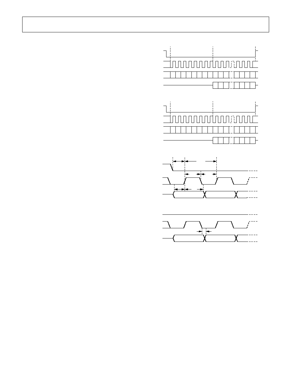
Timing Information
Figure 33 through Figure 35 show some of the various timing
possibilities when the PLL is enabled. The combination of the
settings of N2 and N3 means that the reference clock frequency
may be a multiple of the actual input data rate. Figure 33 through
Figure 35 show, respectively, what the timing looks like when
N2/N3 = 1, 2, and 4.
Figure 36 shows the timing specifications for the AD9779 when the
PLL is disabled. The reference clock is at the DAC output sample
rate. In the example shown in Figure 36, if the PLL is disabled, the
interpolation is 4x.. The set up and hold time for the input data are
with respect to the rising edge of the reference clock which occurs
just before the rising edge of the DATACLK out. Note that if reg
02h, bit2 is set, DATACLK out is inverted so the latching reference
clock edge will occur just before the DATACLK out falling edge.
tH
tS
tD
Refe rence Clock
DATA CLK out
Input Data
Figure 33. Timing Specifications for AD9779, PLL Enabled, Reference Clock = 1x Input Sample Rate
AD9779
Preliminary Technical Data
Rev. PrD | Page 24 of 34
tH
tS
tD
Refe rence Clock
DATA CLK out
Input Data
Figure 34. Timing Specifications for AD9779, PLL Enabled, Reference Clock = 2x Input Sample Rate
tH
tS
tD
Refe rence Clock
DATA CLK out
Input Data
Figure 35. Timing Specifications for AD9779, PLL Enabled, Reference Clock = 4x Input Sample Rate
tH
tS
tD
tS=-2.3ns typ
tH=3.7ns typ
tD=5.5ns typ
Refe rence Clock
DATA CLK out
Input Data
Figure 36. Timing Specifications for AD9779, PLL Disabled, 4x Interpolation
Using Data Delay to Meet Timing Requirements
In order to meet strict timing requirements at input data rates of up
to 250MSPS, the AD9779 has a fine timing feature. Fine timing
adjustments can be made by programming values into the DATA
CLOCK DELAY register (reg 03h, 5:3). By changing the values in
this register, delay can be added to the default delay between the
DACCLK in the DATACLK out. The effect of this is shown in
Figure 37 and Figure 38.
Figure 37. Delay from DACCLK to DATACLK out with CLK DATA DELAY = 000
Figure 38. . Delay from DACCLK to DATACLK out with CLK DATA DELAY = 111
The difference between the default delay of Figure 37 and the
maximum delay shown in Figure 38 is the range programmable via
the DATA CLK DELAY register. The resulting delays when
programming DATA CLK DELAY between 000 and 111 are a
linear extrapolation between these two figures. (typically 300ps-
400ps per increment to DATA CLK DELAY).

Preliminary Technical Data
AD9779
Rev. PrD | Page 25 of 34
Interpolation Filter Architecture
The AD9779 can provide up to 8◊ interpolation or disable the
interpolation filters entirely. The coefficients of the low pass filters
and the inverse sinc filter are given in Table 5, Table 6, Table 7, and
Table 8. Spectral plots for the filter responses are given in Figure 3,
Figure 4, and Figure 5.
With the interpolation filter and modulator combined, the
incoming signal can be placed anywhere within the Nyquist region
of the DAC output sample rate. Where the input signal is complex,
this architecture allows modulation of the input signal to positive
or negative Nyquist regions (refer to Table 13).
The Nyquist regions up to 4◊ the input data rate can be seen in
Figure 39.
DC
1◊
4◊
3◊
2◊
-2◊
-3◊
-4◊
-1◊
1 2 3 4
-1
-2
5
7 8
6
-3
-4
-5
-6
-7
-8
Figure 39. Nyquist Zones
Figure 3, Figure 4 and Figure 5 show the low pass response of the
digital filters with no modulation used. By turning on the
modulation feature, the response of the digital filters can be tuned
to any Nyquist zone within the DAC bandwidth. As an example,
Figure 40 to Figure 46 show the odd mode filter responses (refer to
Table 13 for odd/even mode filter responses).
-4
-3
-2
-1
0
1
2
3
4
-100
-90
-80
-70
-60
-50
-40
-30
-20
-10
0
10
Figure 40. Interpolation/Modulation Combination of -4f
DAC
/8
Filter in Odd Mode
-4
-3
-2
-1
0
1
2
3
4
-100
-90
-80
-70
-60
-50
-40
-30
-20
-10
0
10
Figure 41. Interpolation/Modulation Combination of -3f
DAC
/8
Filter in Odd Mode
-4
-3
-2
-1
0
1
2
3
4
-100
-90
-80
-70
-60
-50
-40
-30
-20
-10
0
10
Figure 42. Interpolation/Modulation Combination of -2f
DAC
/8
Filter in Odd Mode
-4
-3
-2
-1
0
1
2
3
4
-100
-90
-80
-70
-60
-50
-40
-30
-20
-10
0
10
Figure 43. Interpolation/Modulation Combination of -1f
DAC
/8
Filter in Odd Mode

AD9779
Preliminary Technical Data
Rev. PrD | Page 26 of 34
-4
-3
-2
-1
0
1
2
3
4
-100
-90
-80
-70
-60
-50
-40
-30
-20
-10
0
10
Figure 44. Interpolation/Modulation Combination of f
DAC
/8
Filter in Odd Mode
-4
-3
-2
-1
0
1
2
3
4
-100
-90
-80
-70
-60
-50
-40
-30
-20
-10
0
10
Figure 45. Interpolation/Modulation Combination of 2f
DAC
/8
Filter in Odd Mode
-4
-3
-2
-1
0
1
2
3
4
-100
-90
-80
-70
-60
-50
-40
-30
-20
-10
0
10
Figure 46. Interpolation/Modulation Combination of 3f
DAC
/8
Filter in Odd Mode
Even mode filter responses allow the passband to be centered
around ±0.5, ±1.5, ±2.5 and ±3.5 F
DATA
. Switching from and odd
mode response to an even mode filter response does not modulate
the signal. Instead, the pass band is simply shifted. As an example,
picture the response of Figure 46, and assume the signal in band is
a complex signal over the bandwidth 3.2 to 3.3◊F
DATA
. If the even
mode filter response is then selected, the pass band will now be
centered at 3.5◊F
DATA
. However, the signal will still remain at the
same place in the spectrum. The even/odd mode capability allows
the passband to be placed anywhere in the DAC Nyquist
bandwidth.
The AD9779 is a dual DAC with an internal complex modulator
built into the interpolating filter response. The modulator can be
set to a real or a complex mode by programming register 02h, bit 5.
In the default mode, bit 5 is set to zero and the modulation is
complex. The AD9779 then expects the real and the imaginary
components of a complex signal at digital input ports one and two
(I and Q respectively). The DAC outputs will then represent the
real and imaginary components of the input signal, modulated by
the complex carrier F
DAC
/2, F
DAC
/4 or F
DAC
/8.
With Bit 5 set to one, the modulation is real. The Q channel is shut
off and it's value at the modulator inputs replaced with zero. The
output spectrum at either the IDAC or the QDAC will then
represent the signal at digital input port one, real modulated by the
internal digital carrier (F
DAC
/2, F
DAC
/4 or F
DAC
/8).

Preliminary Technical Data
AD9779
Rev. PrD | Page 27 of 34
EVALUATION BOARD SCHEMATICS
Figure 47. AD9779 Eval Board, Rev B , Power Supply Decoupling and SPI Interface
AD9779
Preliminary Technical Data
Rev. PrD | Page 28 of 34
Figure 48. AD9779 Eval Board, Rev B , Circuitry Local to AD9779

Preliminary Technical Data
AD9779
Rev. PrD | Page 29 of 34
Figure 49. AD9779 Eval Board, RevB , AD8349 Quadrature Modulator
AD9779
Preliminary Technical Data
Rev. PrD | Page 30 of 34
Figure 50. AD9779 Eval Board, RevB , DAC Clock Interface
Preliminary Technical Data
AD9779
Rev. PrD | Page 31 of 34
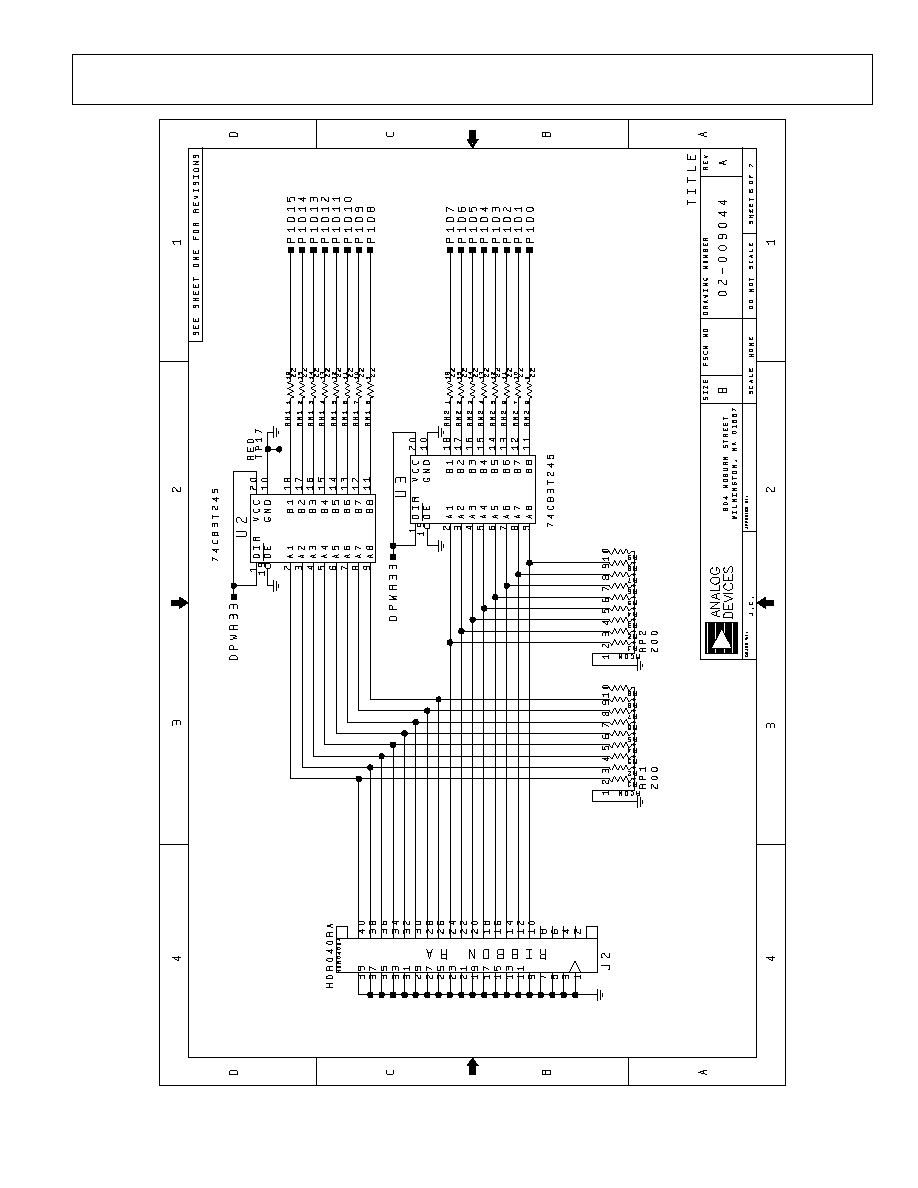
Figure 51. AD9779 Eval Board, RevB , Input Port 1, Digital Input Buffers
AD9779
Preliminary Technical Data
Rev. PrD | Page 32 of 34
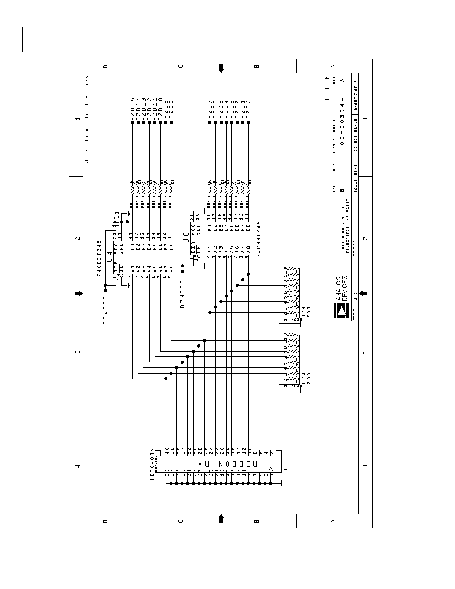
Figure 52. AD9779 Eval Board, RevB , Input Port 2, Digital Input Buffers

Preliminary Technical Data
AD9779
Rev. PrD | Page 33 of 34
Outline Dimensions
AD9779
Preliminary Technical Data
Rev. PrD | Page 34 of 34
ESD CAUTION
ORDERING GUIDE
Table 15: Ordering Guide
ESD (electrostatic discharge) sensitive device. Electrostatic charges as high as 4000 V readily accumulate on the
human body and test equipment and can discharge without detection. Although this product features proprietary
ESD protection circuitry, permanent damage may occur on devices subjected to high energy electrostatic discharges.
Therefore, proper ESD precautions are recommended to avoid performance degradation or loss of functionality.
Model Temperature
Range
Description
AD9779BSV
-40
∞C to +85∞C (Ambient)
100-Lead TQFP, Exposed Paddle
AD9779/PCB
25∞C (Ambient)
Evaluation Board
© 2005 Analog Devices, Inc. All rights reserved. Trademarks and
registered trademarks are the property of their respective owners.
PR05363≠0≠1/05(PrD)