 | –≠–ª–µ–∫—Ç—Ä–æ–Ω–Ω—ã–π –∫–æ–º–ø–æ–Ω–µ–Ω—Ç: AD9875 | –°–∫–∞—á–∞—Ç—å:  PDF PDF  ZIP ZIP |
Document Outline
- Specifications
- Pinout
- PAckage Drawings
- Ordering Guide
- Features
- Applications
- Product Description
- Absolute Maximum Ratings
- Functional Block Diagram
- THERMAL CHARACTERISTICS
- CAUTION
- PIN FUNCTION DESCRIPTIONS
- DEFINITIONS OF SPECIFICATIONS CLOCK JITTER
- GAIN ERROR
- DIFFERENTIAL NONLINEARITY ERROR
- (DNL, NO MISSING CODES)
- INPUT REFERRED NOISE
- SIGNAL-TO-NOISE AND DISTORTION RATIO (SINAD)
- PHASE NOISE
- EFFECTIVE NUMBER OF BITS (ENOB)
- SIGNAL-TO-NOISE RATIO (SNR)
- OUTPUT COMPLIANCE RANGE
- TOTAL HARMONIC DISTORTION (THD)
- SPURIOUS“FREE DYNAMIC RANGE (SFDR)
- POWER SUPPLY REJECTION
- PIPELINE DELAY (LATENCY)
- TRANSMIT PATH
- INTERPOLATION FILTER
- DIGITAL INTERFACE PORT
- PLL-A CLOCK DISTRIBUTION
- D/A CONVERTER
- LOW-PASS FILTER
- ADC
- RECEIVE PATH DESCRIPTION
- PROGRAMMABLE GAIN AMPLIFIER
- CLOCK AND OSCILLATOR CIRCUITRY
- VOLTAGE REGULATOR CONTROLLER
- DIGITAL HPF
- AGC TIMING CONSIDERATIONS
- MSB/LSB Transfers
- REGISTER 4-RECEIVE FILTER SELECTION
- REGISTER 3-CLOCK SOURCE CONFIGURATION
- REGISTER 7-TRANSMIT PATH SETTINGS
- REGISTER 5-RECEIVE FILTER TUNING TARGET
- PCB DESIGN CONSIDERATIONS
- DIAGRAMS
- Transmit Path Block Diagram
- ADC Theory of Operation
- Connections for Fundamental Mode Crystal
- Connections for a 1.3 V Linear Regulator
- AGC Timing
- Transmit Timing Diagram AD9875
- GAIN Programming
- Receive Timing Diagram
- Timing Diagram Register Write to AD9875/AD9876
- Timing Diagram Register Read from AD9875/AD9876
- Serial Register Interface Timing MSB-First
- Serial Register Interface Timing LSB-First

REV. 0
Information furnished by Analog Devices is believed to be accurate and
reliable. However, no responsibility is assumed by Analog Devices for its
use, nor for any infringements of patents or other rights of third parties that
may result from its use. No license is granted by implication or otherwise
under any patent or patent rights of Analog Devices.
AD9875
One Technology Way, P.O. Box 9106, Norwood, MA 02062-9106, U.S.A.
Tel: 781/329-4700
www.analog.com
Fax: 781/326-8703
© Analog Devices, Inc., 2001
a
Broadband Modem
Mixed-Signal Front End
FUNCTIONAL BLOCK DIAGRAM
REGISTER
CONTROL
Rx
MUX
ADC
PGA
LPF
PGA
TxDAC+
Kx INTERPOLATION
LPF/BPF
Tx
MUX
PLL-A
L
PLL-B
M/N
VRC
3
10
10
10
AD9875
Tx+
Tx≠
GATE
FB
OSCIN
XTAL
Rx+
Rx≠
PWR DN
Tx QUIET
GAIN
Tx [5:0]
Tx SYNC
CLK-A
CLK-B
Rx SYNC
Rx [5:0]
SPORT
V
REF
CLOCK GEN
PRODUCT DESCRIPTION
The AD9875 is a single supply Broadband modem mixed-
signal front end (MxFE) IC. The devices contain a transmit
path Interpolation Filter and DAC, and a receive path PGA,
LPF and ADC supporting a variety of Broadband modem
applications. Also on-chip is a PLL clock multiplier that pro-
vides all required clocks from a single crystal or clock input.
The AD9875 provides 10-bit converter performance on both
the Tx and Rx paths.
The TxDAC+ uses a selectable digital 2
◊
or 4
◊
interpolation
low-pass or band-pass filter to further oversample transmit
data and reduce the complexity of analog reconstruction filtering.
The transmit path signal bandwidth can be as high as 26 MHz
at an input data rate of 64 MSPS. The 10-bit DAC provides
differential current outputs for optimum noise and distortion
performance. The DAC full-scale current can be adjusted
from 2 mA to 20 mA by a single resistor, providing 20 dB of
additional gain range.
The receive path consists of a PGA, LPF, and ADC. The two-stage
PGA has a gain range of ≠6 dB to +36 dB, and is programmable
in 2 dB steps, adding 42 dB of dynamic range to the receive path.
MxFE is a trademark of Analog Devices, Inc.
TxDAC+ is a registered trademark of Analog Devices, Inc.
The receive path LPF cutoff frequency can be programmed to either
12 MHz or 26 MHz. The filter cutoff frequency can also be tuned
or bypassed where filter requirements differ. The 10-bit ADC uses
a multistage differential pipeline architecture to achieve excellent
dynamic performance with low power consumption.
The AD9875 provides a voltage regulator controller (VRC) that
can be used with an external power MOSFET transistor to form
a cost-effective 1.3 V linear regulator.
The digital transmit and receive ports are each multiplexed to a
bus width of 5/6 bits and are clocked at a frequency of twice the
10-bit word rate.
The AD9875 ADC and/or DAC can also be used at higher
sampling rates as high as 64 MSPS in a 5-bit resolution non-
multiplexed mode.
The AD9875 is pin-compatible with the 12-bit AD9876. Both are
available in a space-saving 48-lead LQFP package. They are speci-
fied over the industrial (≠40
∞
C to +85
∞
C) temperature range.
FEATURES
Low Cost 3.3 V-CMOS Mixed-Signal Front End (MxFETM)
Converter for Broadband Modems
10-/12-Bit D/A Converter (TxDAC+
Æ
)
64/32 MSPS Input Word Rate
2 /4 Interpolating LPF or BPF Transmit Filter
128 MSPS DAC Output Update Rate
Wide (26 MHz) Transmit Bandwidth
Power-Down Mode
10-/12-Bit, 50 MSPS A/D Converter
Fourth Order Low-Pass Filter 12 MHz or 26 MHz
with Bypass
≠6 dB to +36 dB Programmable Gain Amplifier
Internal Clock Multiplier (PLL)
Clock Outputs
Voltage Regulator Controller
48-Lead LQFP Package
APPLICATIONS
Powerline Networking
Home Phone Networking
xDSL
Broadband Wireless
Home RF

REV. 0
≠2≠
AD9875≠SPECIFICATIONS
Test
Parameter
Temp
Level
Min
Typ
Max
Unit
OSC IN CHARACTERISTICS
Frequency Range
Full
II
10
64
MHz
Duty Cycle
25
∞
C
II
40
50
60
%
Input Capacitance
25
∞
C
III
3
pF
Input Impedance
25
∞
C
III
100
M
CLOCK OUTPUT CHARACTERISTICS
CLKA Jitter (f
CLKA
Derived from PLL)
25
∞
C
III
14
ps rms
CLKA Duty Cycle
25
∞
C
III
50
±
5
%
CLKB Jitter (f
CLKB
Derived from PLL)
25
∞
C
III
33
ps rms
CLKB Duty Cycle
25
∞
C
III
50
±
5
%
Tx CHARACTERISTICS
Tx Path Latency, 4
◊
Interpolation
Full
II
82
f
DAC
Cycles
Interpolation Filter Bandwidth (≠0.1 dB)
4
◊
Interpolation, LPF
Full
II
13
MHz
2
◊
Interpolation, LPF
Full
II
26
MHz
TxDAC
Resolution
Full
II
10
Bits
Conversion Rate
Full
II
10
128
MHz
Full-Scale Output Current
Full
II
2
10
20
mA
Voltage Compliance Range
Full
II
≠0.5
+1.5
V
Gain Error
Full
II
≠5
±
2
+5
% FS
Output Offset
Full
II
0
7
19
µ
A
Differential Nonlinearity
25
∞
C
III
0.5
LSB
Integral Nonlinearity
25
∞
C
III
1
LSB
Output Capacitance
25
∞
C
III
5
pF
Phase Noise @ 1 kHz Offset, 10 MHz Signal
25
∞
C
III
≠90
dBc/Hz
Signal-to-Noise and Distortion (SINAD)
10 MHz Analog Out AD9875 (20 MHz BW)
Full
I
59
61
dB
Wideband SFDR (to Nyquist, 64 MHz Max)
25
∞
C
III
5 MHz Analog Out
25
∞
C
III
78
dBc
10 MHz Analog Out
25
∞
C
III
72
dBc
Narrowband SFDR (3 MHz Window):
10 MHz Analog Out
25
∞
C
III
80
dBc
IMD (f1 = 6.9 MHz, f2 = 7.1 MHz)
25
∞
C
III
≠76
dBFS
Rx PATH CHARACTERISTICS
Resolution
Full
II
10
Bits
Conversion Rate
Full
II
7.5
55
MHz
Pipeline Delay, ADC Clock Cycles
Full
II
5.5
Cycles
DC Accuracy
Differential Nonlinearity
25
∞
C
II
≠1.0
±
0.25
+1.0
LSB
Integral Nonlinearity
25
∞
C
II
≠2.0
±
0.5
+2.0
LSB
Dynamic Performance
(A
IN
= ≠0.5 dBFS, f = 5 MHz)
@ f
OSCIN
= 32 MHz
Signal-to-Noise and Distortion Ratio (SINAD)
25
∞
C
III
59.6
dB
Effective Number of Bits (ENOB)
25
∞
C
III
9.5
Bits
Signal-to-Noise Ratio (SNR)
25
∞
C
III
60
dB
Total Harmonic Distortion (THD)
25
∞
C
III
≠65
dB
Spurious Free Dynamic Range (SFDR)
25
∞
C
III
68
dB
Dynamic Performance
(A
IN
= ≠0.5 dBFS, f = 10 MHz)
@ F
PLLB/2
= 50 MHz
Signal-to-Noise and Distortion Ratio (SINAD)
25
∞
C
III
54
dB
Effective Number of Bits (ENOB)
25
∞
C
III
8.6
Bits
Signal-to-Noise Ratio (SNR)
25
∞
C
III
55
dB
Total Harmonic Distortion (THD)
25
∞
C
III
≠61
dB
Spurious Free Dynamic Range (SFDR)
25
∞
C
III
68
dB
(V
S
= 3.3 V 10%, f
OSCIN
= 32 MHz, f
DAC
= 128 MHz, Gain = ≠6 dB, R
SET
= 4.02 k
,
100
DAC single-ended load, unless otherwise noted. )

REV. 0
≠3≠
AD9875
Test
Parameter
Temp
Level
Min
Typ
Max
Unit
Rx PATH GAIN/OFFSET
Minimum Programmable Gain
25
∞
C
III
≠6
dB
Maximum Programmable Gain
(12 MHz Filter)
25
∞
C
III
36
dB
(26 MHz Filter)
25
∞
C
III
30
dB
Gain Step Size
25
∞
C
III
2
dB
Gain Step Accuracy
25
∞
C
III
±
0.4
dB
Gain Range Error
25
∞
C
III
±
1.0
dB
Offset Error, PGA Gain = 0 dB (AD9875)
25
∞
C
III
±
4.0
LSB
Absolute Gain Error, PGA Gain = 0 dB
25
∞
C
III
±
0.8
dB
Rx PATH INPUT CHARACTERISTICS
Input Voltage Range
25
∞
C
III
4
Vppd
Input Capacitance
25
∞
C
III
4
pF
Differential Input Resistance
25
∞
C
III
270
Input Bandwidth (≠3 dB)
25
∞
C
III
50
MHz
Input Referred Noise (at +36 dB Gain with Filter)
25
∞
C
III
16
µ
V rms
Input Referred Noise (at ≠6 dB Gain with Filter)
25
∞
C
III
684
µ
V rms
Common-Mode Rejection
25
∞
C
III
40
dB
Rx PATH LPF (Low Cutoff Frequency)
Cutoff Frequency
25
∞
C
III
12
MHz
Cutoff Frequency Variation
25
∞
C
III
±
7
%
Attenuation @ 22 MHz
25
∞
C
III
20
dB
Passband Ripple
25
∞
C
III
±
1.0
dB
Group Delay Variation
25
∞
C
III
30
ns
Settling Time
(to 1% FS, Min to Max Gain Change)
25
∞
C
III
150
ns
Total Harmonic Distortion at Max Gain (THD)
25
∞
C
III
≠68
dBc
Rx PATH LPF (High Cutoff Frequency)
Cutoff Frequency
25
∞
C
III
26
MHz
Cutoff Frequency Variation
25
∞
C
III
±
7
%
Attenuation @ 44 MHz
25
∞
C
III
20
dB
Passband Ripple
25
∞
C
III
±
1.2
dB
Group Delay Variation
25
∞
C
III
15
ns
Settling Time
(to 1% FS, Min to Max Gain Change)
25
∞
C
III
80
ns
Total Harmonic Distortion at Max Gain (THD)
25
∞
C
III
≠65
dBc
Rx PATH DIGITAL HPF
Latency (ADC Clock Source Cycles)
Full
II
1
Cycle
Roll-Off in Stopband
Full
II
6
dB/Octave
≠3 dB Frequency
Full
II
f
ADC
/400
Hz
Rx PATH DISTORTION PERFORMANCE
IMD: f1 = 6.9 MHz, f2 = 7.1 MHz
12 MHz Filter: 0 dB
25
∞
C
III
≠65
dBc
: 30 dB
25
∞
C
III
≠57
dBc
28 MHz Filter: 0 dB
25
∞
C
III
≠65
dBc
: 30 dB
25
∞
C
III
≠56
dBc
POWER-DOWN/DISABLE TIMING
Power-Up Delay (Power-Down-to-Active)
DAC
25
∞
C
II
40
µ
s
PLL
25
∞
C
II
10
µ
s
ADC
25
∞
C
II
1000
µ
s
PGA
25
∞
C
II
1
µ
s
LPF
25
∞
C
II
1
µ
s
Interpolator
25
∞
C
II
200
ns
VRC
25
∞
C
II
2
µ
s
Minimum RESET Pulsewidth Low (t
RL
)
Full
III
5
f
OSCIN
Cycle
DAC I
OUT
Off after Tx QUIET Asserted
25
∞
C
II
200
ns
DAC I
OUT
On after Tx QUIET Deasserted
25
∞
C
II
1
µ
s
Power-Down Delay (Active-to-Power-Down)
DAC
25
∞
C
II
400
ns
Interpolator
25
∞
C
II
200
ns

REV. 0
≠4≠
AD9875≠SPECIFICATIONS
Test
Parameter
Temp
Level
Min
Typ
Max
Unit
Tx PATH INTERFACE
Maximum Input Nibble Rate, 2
◊
Interp.
Full
II
128
MHz
Tx-Set Up Time (t
SU
)
Full
II
3.0
ns
Tx-Hold Time (t
HD
)
Full
II
0
ns
Rx PATH INTERFACE
Maximum Output Nibble Rate
Full
I
110
MHz
Rx-DataValid Time (t
VT
)
Full
II
3.0
ns
Rx-Data Hold Time (t
HT
)
Full
II
1.5
ns
CMOS LOGIC INPUTS
Logic "1" Voltage
Full
II
V
DRVDD
≠ 0.7
V
Logic "0" Voltage
Full
II
0.4
V
Logic "1" Current
Full
II
12
µ
A
Logic "0" Current
Full
II
12
µ
A
Input Capacitance
25
∞
C
III
3
µ
F
CMOS LOGIC OUTPUTS (1 mA Load)
Logic "1" Voltage
Full
II
V
DRVDD
≠ 0.6
V
Logic "0" Voltage
Full
II
0.4
V
Digital Output Rise/Fall Time
Full
II
1.5
2.5
ns
POWER SUPPLY
All Blocks Powered Up
I
S_TOTAL
(Total Supply Current)
Full
I
262
288
mA
I
S_TOTAL
(Tx_QUIET Pin Asserted)
25
∞
C
III
172
mA
Digital Supply Current (I
DRVDD
+ I
DVDD
)
25
∞
C
III
77
mA
Analog Supply Current (I
AVDD
)
25
∞
C
III
185
mA
Power Consumption of Functional Blocks:
Rx LPF
25
∞
C
III
110
mA
ADC and FPGA
25
∞
C
III
55
mA
Rx Reference
25
∞
C
III
2
mA
Interpolator
25
∞
C
III
33
mA
DAC
25
∞
C
III
18
mA
PLL-B
25
∞
C
III
8
mA
PLL-A
25
∞
C
III
24
mA
Voltage Regulator Controller
25
∞
C
III
1
mA
All Blocks Powered Down
Supply Current I
S
, f
OSCIN
= 32 MHz
Full
II
19
22
mA
Supply Current I
S
, f
OSCIN
Idle
Full
II
10
12
mA
Power Supply Rejection
Tx Path (
V
S
= 10%)
25
∞
C
III
62
dB
Rx Path (
V
S
= 10%)
25
∞
C
III
54
dB
SERIAL CONTROL BUS
Maximum SCLK Frequency (f
SCLK
)
Full
II
25
MHz
Clock Pulsewidth High (t
PWH
)
Full
II
18
ns
Clock Pulsewidth Low (t
PWL
)
Full
II
18
ns
Clock Rise/Fall Time
Full
II
1
ms
Data/Chip-Select Setup Time (t
DS
)
Full
II
25
ns
Data Hold Time (t
DH
)
Full
II
0
ns
Data Valid Time (t
DV
)
Full
II
20
ns
RECEIVE-TO-TRANSMIT ISOLATION
(10 MHz, Full-Scale Sinewave Output/Output)
Isolation: Tx Path to Rx Path, Gain = +36 dB
25
∞
C
III
≠75
dB
Isolation: Rx Path to Tx Path, Gain = ≠6 dB
25
∞
C
III
≠70
dB
VOLTAGE REGULATOR CONTROLLER
Output Voltage (V
FB
with SI2301 Connected)
Full
I
1.25
1.30
1.35
V
Line Regulation (
V
FB%
/
V
DVDD%
◊
100%)
25
∞
C
III
100
%
Load Regulation (
V
FB
/
I
LOAD
)
25
∞
C
III
60
m
Maximum Load Current (I
LOAD
)
Full
II
250
mA
Specifications subject to change without notice.
(continued)
REV. 0
AD9875
≠5≠
CAUTION
ESD (electrostatic discharge) sensitive device. Electrostatic charges as high as 4000 V readily
accumulate on the human body and test equipment and can discharge without detection. Although
the AD9875 features proprietary ESD protection circuitry, permanent damage may occur on
devices subjected to high-energy electrostatic discharges. Therefore, proper ESD precautions are
recommended to avoid performance degradation or loss of functionality.
Model
Temperature Range
Package Description
Package Option
AD9875BST
≠40
∞
C to +85
∞
C
48-Lead LQFP
ST-48
AD9875-EB
≠40
∞
C to +85
∞
C
Evaluation Board
AD9875BSTRL
≠40
∞
C to +85
∞
C
BST Reel
ABSOLUTE MAXIMUM RATINGS
*
Power Supply (V
S
) . . . . . . . . . . . . . . . . . . . . . . . . . . . . . 3.9 V
Digital Output Current . . . . . . . . . . . . . . . . . . . . . . . . . 5 mA
Digital Inputs . . . . . . . . . . . . . . . . . ≠0.3 V to DRVDD 0.3 V
Analog Inputs . . . . . . . . . . . . . . . . . . ≠0.3 V to AVDD 0.3 V
Operating Temperature . . . . . . . . . . . . . . . . . ≠40
∞
C to +85
∞
C
Maximum Junction Temperature . . . . . . . . . . . . . . . . 150
∞
C
Storage Temperature . . . . . . . . . . . . . . . . . . ≠65
∞
C to +150
∞
C
Lead Temperature (Soldering 10 sec) . . . . . . . . . . . . . 300
∞
C
*Stresses greater than those listed under Absolute Maximum Ratings may cause
permanent damage to the device. This is a stress rating only; functional operation
of the device at these or any other conditions above those indicated in the
operational section of this specification is not implied. Exposure to absolute
maximum rating conditions for extended periods may affect device reliability.
EXPLANATION OF TEST LEVELS
I ≠ Devices are 100% production tested at 25
∞
C and guaran-
teed by design and characterization testing for industrial
operating temperature range (≠40
∞
C to +85
∞
C).
II ≠ Parameter is guaranteed by design and/or characterization
testing.
III ≠ Parameter is a typical value only.
THERMAL CHARACTERISTICS
Thermal Resistance
48-Lead LQFP
JA
= 57
∞
C/W
JC
= 28
∞
C/W
WARNING!
ESD SENSITIVE DEVICE
ORDERING GUIDE
REV. 0
AD9875
≠6≠
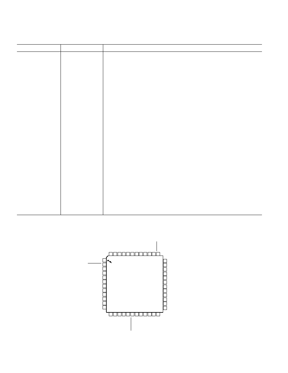
PIN CONFIGURATION
36
35
34
33
32
31
30
29
28
27
26
25
DRVSS
DRVDD
Rx [0]
Rx [1]
Rx [2]
Rx [3]
Rx [4]
Rx [5]
Rx SYNC
CLK-B
CLK-A
Tx SYNC
13 14 15 16 17 18 19 20 21 22 23 24
DVSS
DVDD
FB
GATE
GAIN
Tx QUIET
Tx [5]
Tx [4]
Tx [3]
Tx [2]
Tx [1]
Tx [0]
1
2
3
4
5
6
7
8
9
10
11
12
OSCIN
SENABLE
SCLK
SDATA
AVDD
AVSS
Tx+
Tx≠
AVSS
FSADJ
REFIO
PWR DN
48 47 46 45 44
39 38 37
43 42 41 40
XTAL
AVDD
AVSS
Rx
≠
Rx+
AVSS
AVSS
REFT
REFB
AVSS
AVDD
RESET
PIN 1
IDENTIFIER
TOP VIEW
(Not to Scale)
AD9875
Pin
Name
Function
1
OSCIN
Crystal Oscillator Inverter Input
2
SENABLE
Serial Bus Enable Input
3
SCLK
Serial Bus Clock Input
4
SDATA
Serial Bus Data I/O
5, 38, 47
AVDD
Analog 3.3 V Power Supply
6, 9, 39, 42, 43, 46
AVSS
Analog Ground
7
Tx+
Transmit DAC+ Output
8
Tx≠
Transmit DAC≠ Output
10
FSADJ
DAC Full-Scale Output Current Adjust with External Resistor
11
REFIO
DAC Bandgap Decoupling Node
12
PWR DN
Power-Down Input
13
DVSS
Digital Ground
14
DVDD
Digital 3.3 V Power Supply
15
FB
Regulator Feedback Input
16
GATE
Regulator Output to FET Gate
17
GAIN
Transmit Data Port (Tx[5:0]) Mode Select Input
18
Tx QUIET
Transmit Quiet Input
19≠24
Tx[5:0]
Transmit Data Input
25
Tx SYNC
Transmit Synchronization Strobe Input
26
CLK-A
L
◊
f
OSCIN
Clock Output
27
CLK-B
M/N
◊
f
OSCIN
Clock Output
28
Rx SYNC
Receive Data Synchronization Strobe Output
29≠34
Rx[5:0]
Receive Data Output
35
DRVDD
Digital I/O 3.3 V Power Supply
36
DRVSS
Digital I/O Ground
37
RESET
Reset Input
40
REFB
ADC Reference Decoupling Node
41
REFT
ADC Reference Decoupling Node
44
Rx+
Receive Path + Input
45
Rx≠
Receive Path ≠ Input
48
XTAL
Crystal Oscillator Inverter Output
PIN FUNCTION DESCRIPTIONS

REV. 0
AD9875
≠7≠
DEFINITIONS OF SPECIFICATIONS
CLOCK JITTER
The clock jitter is a measure of the intrinsic jitter of the PLL
generated clocks. It is a measure of the jitter from one rising
and of the clock with respect to another edge of the clock nine
cycles later.
DIFFERENTIAL NONLINEARITY ERROR
(DNL, NO MISSING CODES)
An ideal converter exhibits code transitions that are exactly 1 LSB
apart. DNL is the deviation from this ideal value. Guaranteed
no missing codes to 10-bit resolution indicates that all 1024
codes respectively, must be present over all operating ranges.
INTEGRAL NONLINEARITY ERROR (INL)
Linearity error refers to the deviation of each individual code
from a line drawn from "negative full scale" through "positive
full scale." The point used as "negative full scale" occurs 1/2 LSB
before the first code transition. "positive full scale" is defined as
a level 1 1/2 LSB beyond the last code transition. The deviation
is measured from the middle of each particular code to the true
straight line.
PHASE NOISE
Single-sideband phase noise power density is specified relative
to the carrier (dBc/Hz) at a given frequency offset (1 kHz) from
the carrier. Phase noise can be measured directly on a generated
single tone with a spectrum analyzer that supports noise marker
measurements. It detects the relative power between the carrier
and the offset (1 kHz) sideband noise and takes the resolution
bandwidth (rbw) into account by subtracting 10 log(rbw). It
also adds a correction factor that compensates for the imple-
mentation of the resolution bandwidth, log display and detector
characteristic.
OUTPUT COMPLIANCE RANGE
The range of allowable voltage at the output of a current-output
DAC. Operation beyond the maximum compliance limits may
cause either output stage saturation, resulting in nonlinear per-
formance or breakdown.
SPURIOUS≠FREE DYNAMIC RANGE (SFDR)
The difference, in dB, between the rms amplitude of the DACs
output signal (or ADC's input signal) and the peak spurious
signal over the specified bandwidth (Nyquist bandwidth unless
otherwise noted).
PIPELINE DELAY (LATENCY)
The number of clock cycles between conversion initiation and
the associated output data being made available.
OFFSET ERROR
First transition should occur for an analog value 1/2 LSB above
negative full scale. Offset error is defined as the deviation of the
actual transition from that point.
GAIN ERROR
The first code transition should occur at an analog value 1/2 LSB
above negative full scale. The last transition should occur for an
analog value 1 1/2 LSB below the nominal full scale. Gain error
is the deviation of the actual difference between first and last
code transitions and the ideal difference between first and last
code transitions.
INPUT REFERRED NOISE
The RMS output noise is measured using histogram techniques.
The ADC output codes' standard deviation is calculated in LSB,
and converted to an equivalent voltage. This results in a noise
figure that can be directly referred to the Rx input of the AD9875.
SIGNAL-TO-NOISE AND DISTORTION RATIO (SINAD)
SINAD is the ratio of the RMS value of the measured input
signal to the RMS sum of all other spectral components below
the Nyquist frequency, including harmonics but excluding dc.
The value for SINAD is expressed in decibels.
EFFECTIVE NUMBER OF BITS (ENOB)
For a sine wave, SINAD can be expressed in terms of the num-
ber of bits. Using the following formula,
N = (SINAD ≠ 1.76) dB/6.02
it is possible to get a measure of performance expressed as N,
the effective number of bits.
SIGNAL-TO-NOISE RATIO (SNR)
SNR is the ratio of the rms value of the measured input signal to
the rms sum of all other spectral components below the Nyquist
frequency, excluding harmonics and dc. The value for SNR is
expressed in decibels.
TOTAL HARMONIC DISTORTION (THD)
THD is the ratio of the rms sum of the first six harmonic com-
ponents to the rms value of the measured input signal and is
expressed as a percentage or in decibels.
POWER SUPPLY REJECTION
Power Supply Rejection specifies the converters maximum
full-scale change when the supplies are varied from nominal to
minimum and maximum specified voltages.

REV. 0
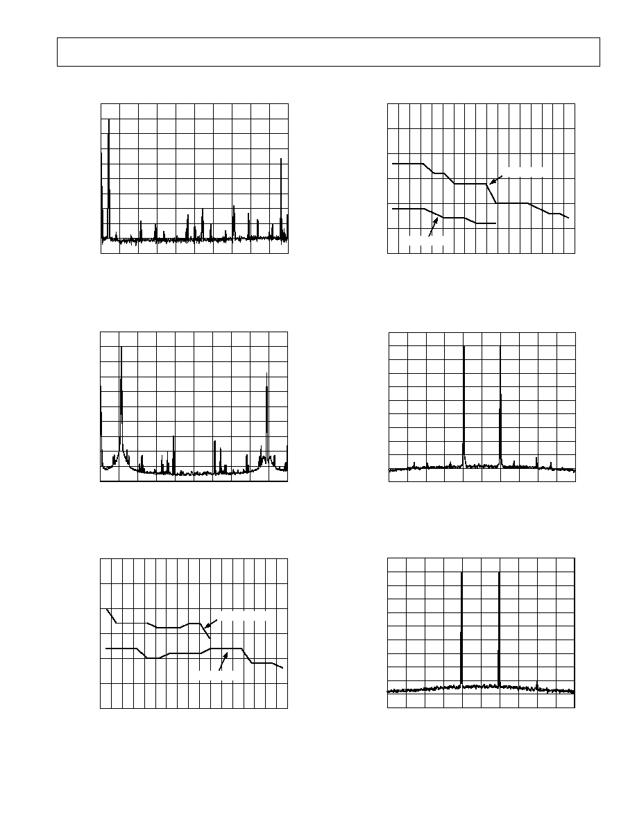
≠Typical Tx Digital Filter Performance Characteristics
≠8≠
NORMALIZED ≠ fs
10
≠60
≠100
0
≠50
≠70
≠80
≠10
≠30
≠20
≠40
≠90
0.0
0.1
0.2
0.3
0.4
0.5
0.6
0.7
0.8
0.9
1.0
MAGNITUDE
≠
dB
INTERPOLATION
FILTER
INCLUDING SIN(X)/X
TPC 1. 4 Low-Pass Interpolation Filter
NORMALIZED ≠ f
S
10
≠60
≠100
0
≠50
≠70
≠80
≠10
≠30
≠20
≠40
≠90
0.0
0.1
0.2
0.3
0.4
0.5
0.6
0.7
0.8
0.9
1.0
MAGNITUDE
≠
dB
INTERPOLATION
FILTER
INCLUDING SIN(X)/X
TPC 2. 2 Low-Pass Interpolation Filter
NORMALIZED ≠ f
S
10
≠60
≠100
0
≠50
≠70
≠80
≠10
≠30
≠20
≠40
≠90
0.0
0.1
0.2
0.3
0.4
0.5
0.6
0.7
0.8
0.9
1.0
MAGNITUDE
≠
dB
INTERPOLATION
FILTER
INCLUDING SIN(X)/X
TPC 3. 4 Bandpass Interpolation Filter, f
S
/2 Modulation,
Adjacent Image Preserved
NORMALIZED ≠ f
S
≠60
≠100
≠50
≠70
≠80
≠30
≠40
≠90
0.0
0.1
0.2
0.3
0.4
0.5
0.6
0.7
0.8
0.9
1.0
MAGNITUDE
≠
dB
10
0
≠10
≠20
INTERPOLATION
FILTER
INCLUDING SIN(X)/X
TPC 4. 2 Bandpass Interpolation Filter, f
S
/2 Modulation,
Adjacent Image Preserved
NORMALIZED ≠ f
S
10
≠60
≠100
0
≠50
≠70
≠80
≠10
≠30
≠20
≠40
≠90
0.0
0.1
0.2
0.3
0.4
0.5
0.6
0.7
0.8
0.9
1.0
MAGNITUDE
≠
dB
INTERPOLATION
FILTER
INCLUDING SIN(X)/X
TPC 5. 4 Bandpass Interpolation Filter, f
S
/4 Modulation,
Lower Image Preserved
NORMALIZED ≠ f
S
10
≠60
≠100
0
≠50
≠70
≠80
≠10
≠30
≠20
≠40
≠90
0.0
0.1
0.2
0.3
0.4
0.5
0.6
0.7
0.8
0.9
1.0
MAGNITUDE
≠
dB
INCLUDING SIN(X)/X
INTERPOLATION
FILTER
TPC 6. 4 Bandpass Interpolation Filter, f
S
/4 Modulation,
Upper Image Preserved
AD9875
REV. 0
AD9875
≠9≠
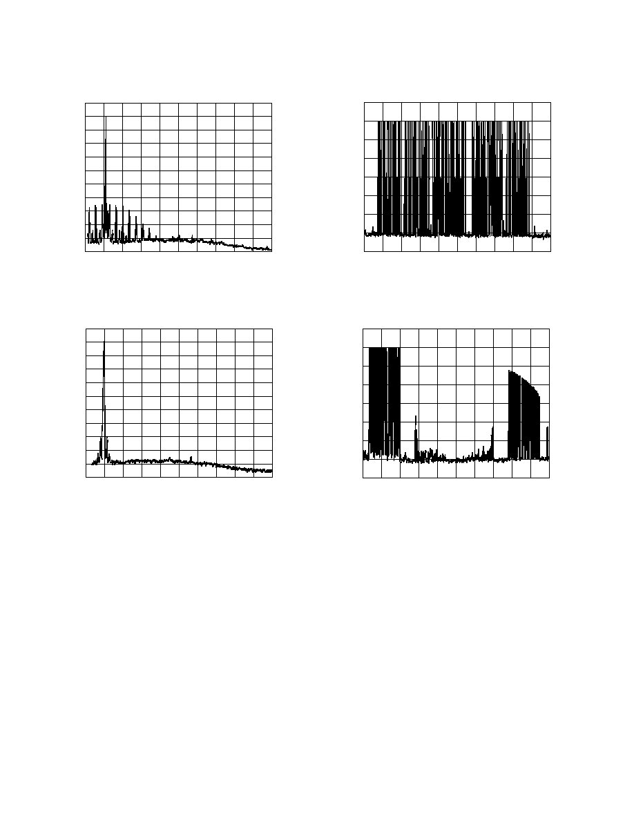
FREQUENCY ≠ MHz
0
13
26
38
51
64
77
90
102
115
128
0
10
≠10
≠20
≠30
≠40
≠50
≠60
≠70
≠80
≠90
MAGNITUDE
≠
dBc
TPC 7. Single Tone Spectral Plot @ f
DATA
= 32 MSPS,
f
OUT
= 5 MHz, 4
LPF
FREQUENCY ≠ MHz
0
10
≠10
≠20
≠30
≠40
≠50
≠60
≠70
≠80
≠90
MAGNITUDE
≠
dBc
0
10
20
30
40
50
60
70
80
90
100
TPC 8. Single Tone Spectral Plot @ f
DATA
= 50 MSPS,
f
OUT
= 11 MHz, 2
LPF
f
OUT
≠ MHz
90
85
60
80
75
70
65
1
3
2
4
6
5
7
9
8
10
12
11
13
15
14
16
18
17
MAGNITUDE
≠
dBc
f
DATA
= 32MSPS
f
DATA
= 50MSPS
TPC 9. "In Band" SFDR vs. f
OUT
@ f
DATA
= 32 MSPS
and 50 MSPS
f
OUT
≠ MHz
90
85
60
80
75
70
65
1
3
2
4
6
5
7
9
8
10
12
11
13
15
14
16
18
17
MAGNITUDE
≠
dBc
f
DATA
= 50MSPS
f
DATA
= 50MSPS
TPC 10. "Out of Band" SFDR vs. f
OUT
@ f
DATA
= 32 MSPS
and 50 MSPS
FREQUENCY ≠ MHz
0
10
≠10
≠20
≠30
≠40
≠50
≠60
≠70
≠80
≠90
≠100
7.5
6.5
6.6
6.7
6.8
6.9
7.0
7.1
7.2
7.3
7.4
MAGNITUDE
≠
dBc
TPC 11. Dual Tone Spectral Plot @ f
DATA
= 32 MSPS,
f
OUT
= 6.9 MHz and 7.1 MHz, 4
LPF
FREQUENCY ≠ MHz
0
10
≠10
≠20
≠30
≠40
≠50
≠60
≠70
≠80
≠90
≠100
7.5
6.5
6.6
6.7
6.8
6.9
7.0
7.1
7.2
7.3
7.4
MAGNITUDE
≠
dBc
TPC 12. Dual Tone Spectral Plot @ f
DATA
= 50 MSPS,
f
OUT
= 6.9 MHz and 7.1 MHz, 2
LPF
Typical AC Characteristics Curves for TxDAC
(R
SET
= 4.02 k
, R
DAC
= 100 )
REV. 0
AD9875
≠10≠
FREQUENCY OFFSET ≠ kHz
0
10
≠10
≠20
≠30
≠40
≠50
≠60
≠70
≠80
≠90
≠100
MAGNITUDE
≠
dBc
≠1
0
1
2
3
4
5
6
7
8
9
TPC 13. Phase Noise Plot @ f
DATA
= 32 MSPS,
f
OUT
= 10 MHz, 4
LPF
FREQUENCY OFFSET ≠ kHz
0
10
≠10
≠20
≠30
≠40
≠50
≠60
≠70
≠80
≠90
≠100
MAGNITUDE
≠
dBc
≠1
0
1
2
3
4
5
6
7
8
9
TPC 14. Phase Noise Plot @ f
DATA
= 50 MSPS,
f
OUT
= 10 MHz, 2
LPF
FREQUENCY ≠ MHz
0
10
≠10
≠20
≠30
≠40
≠50
≠60
≠70
MAGNITUDE
≠
dBc
3
5
7
9
11
13
15
17
19
21
23
TPC 15. "In Band" Multitone Spectral Plot
@ f
DATA
= 50 MSPS, f
OUT
= k
195 kHz, 2 LPF
3
11
31
21
41
51
61
71
81
91
101
FREQUENCY ≠ MHz
0
10
≠10
≠20
≠30
≠40
≠50
≠60
≠70
MAGNITUDE
≠
dBc
TPC 16. "Wide-Band" Multitone Spectral Plot
@ f
DATA
= 50 MSPS, f
OUT
= k 195 kHz, 2
LPF
Typical AC Characteristics Curves for TxDAC
(R
SET
= 4.02 k
, R
DAC
= 10.0 )
REV. 0
AD9875
≠11≠
20
22
24
26
28
30
34
32
36
38
40
64
80
96
112
128
144
160
176
192
FREQUENCY
≠
MHz
TPC 17. Rx vs. Tuning Target, f
ADC
= 32 MHz, LPF with
Wideband Rx LPF = 1
VGA GAIN ≠ dB
MAGNITUDE
≠
dB
≠0.80
≠0.60
≠0.40
≠0.20
0.00
0.20
0.60
0.40
≠6 ≠4 ≠2 0 2 4 6 8 10 12 14 16 18 20 22 24 26 28 30 32 34 36
TPC 18. PGA Gain Error vs. Gain
8
9
10
11
12
13
15
14
16
17
18
48
64
80
96
112
128
144
160
176
192
FREQUENCY
≠
MHz
TPC 19. f
C
vs. Tuning Target, f
ADC
= 32 MHz, LPF with
Wideband Rx LPF = 0
VGA GAIN ≠ dB
MAGNITUDE
≠
dB
1.5
1.6
1.7
1.8
1.9
2.0
2.2
2.1
2.3
2.4
2.5
≠6 ≠4 ≠2 0 2 4 6 8 10 12 14 16 18 20 22 24 26 28 30 32 34 36
TPC 20. PGA Gain Step Size vs. Gain
Typical AC Characterization Curves for Rx Path
REV. 0
AD9875
≠12≠
1MHz
10MHz
100MHz
10.8MHz
0
LOG MAG
5dB/REF 0dB
≠3.0dB
TPC 21. Rx LPF Frequency Response, Low f
C
Nominal
Tuning Targets
26.5MHz
1MHz
10MHz
100MHz
0
LOG MAG
5dB/REF 0dB
≠3.0dB
TPC 22. Rx LPF Frequency Response, High f
C
Nominal
Tuning Targets
14.5MHz
1MHz
10MHz
100MHz
0
LOG MAG
5dB/REF 0dB
≠3.0dB
TPC 23. Rx LPF Frequency Response, Low f
C
, 0 60 and
0 96 Tuning Targets
9.0MHz
1MHz
10MHz
100MHz
0
DELAY
10ns/REF 0s
72.188ns
TPC 24. Rx LPF Group Delay, Low f
C
Nominal Tuning
Targets
22.5MHz
1MHz
10MHz
100MHz
0
DELAY
5ns/REF 0s
34.431ns
TPC 25. Rx LPF Group Delay, High f
C
, Nominal Tuning
Targets
1MHz
10MHz
100MHz
0
14.5MHz
DELAY
10ns/REF 0s
51.244ns
TPC 26. Rx LPF Group Delay, Low f
C
, 0 60 and 0 96
Tuning Targets
Typical AC Characterization Curves for Rx Path
(f
ADC
= 32 MHz)

REV. 0
AD9875
≠13≠
33.5MHz
1MHz
10MHz
100MHz
0
LOG DELAY
5dB/REF ≠2dB
≠5.1933dB
TPC 27. Rx LPF Frequency Response, High f
C
, 0 60 and
0 96 Tuning Targets
78.8MHz
0
LOG MAG
5dB/REF 0dB
≠3.01dB
10kHz
100kHz
1MHz
TPC 28. Rx HPF Frequency Response, f
ADC
= 32 MHz
ADC CLOCK CYCLES
ADC OUTPUT CODE
600
650
700
750
800
850
900
950
1000
0
5
10
15
20
25
30
35
40
f
ADC
= 50MHz
f
ADC
= 32MHz
TPC 29. Rx Path Setting, 1/2 Scale Rising Step with Gain
Change
29.5MHz
0
1MHz
10MHz
100MHz
LOG DELAY
5ns/REF 0s
29.97ns
TPC 30. Rx LPF Group Delay, High f
C
, 0 60 and 0 96
Tuning Targets
GAIN SETTING
≠
dB
700
600
100
500
400
300
200
0
≠6
14
4
24
34
ADC INPUT RMS NOISE
≠
V
FILTER ENABLED
FILTER BYPASSED
TPC 31. Rx Input Referred Noise vs. Gain @ f
ADC
= 32 MSPS,
f
IN
= 1 MHz
600
650
700
750
800
850
900
950
1000
ADC CLOCK CYCLES
ADC OUTPUT CODE
0
5
10
15
20
25
30
35
40
f
ADC
= 50MHz
f
ADC
= 32MHz
TPC 32. Rx Path Setting, 1/2 Scale Falling Step with Gain
Change
Typical AC Characterization Curves for Rx Path
(f
ADC
= 32 MHz)

REV. 0
AD9875
≠14≠
f
S
≠ MHz
ENOB
10.0
9.0
7.0
10
20
30
40
50
8.0
8.5
9.5
7.5
f
OSCIN
f
PLLB/2
15
25
35
45
TPC 33. Rx Path ENOB vs. f
ADC
f
IN
≠ MHz
ENOB
10.0
9.0
7.0
0
8.0
8.5
9.5
7.5
f
OSCIN
f
PLLB/2
2
4
6
8
10
12
14
16
18
20
TPC 36. Rx Path ENOB vs. f
IN
GAIN ≠ dB
ENOB
10.0
≠6
0
6
12
f
POSCIN
f
PLLB/2
18
24
30
36
9.5
9.0
8.5
8.0
TPC 39. Rx Path ENOB vs. Gain
f
S
≠ MHz
MA
GNITUDE
≠
dB
60
56
48
52
54
58
50
10
20
25
30
15
35
40
45
50
f
OSCIN
f
PLLB/2
TPC 34. Rx Path SNR vs. f
ADC
f
IN
≠ MHz
MA
GNITUDE
≠
dB
0
4
6
8
10
2
12
14
16
18
20
70
60
40
50
55
65
45
f
OSCIN
f
PLLB/2
TPX 37. Rx Path SNR vs. f
IN
GAIN ≠ dB
MAGNITUDE
≠
dB
65
60
45
≠6
6
12
18
50
55
0
24
30
36
f
OSCIN
f
PLLB/2
TPC 40. Rx Path SNR vs. Gain
f
S
≠ MHz
MAGNITUDE
≠
dB
≠50
10
f
OSCIN
f
PLLB/2
15
20
25
30
35
40
45
50
≠55
≠60
≠65
≠70
≠75
≠80
TPC 35. Rx Path THD vs. f
ADC
f
IN
≠ MHz
MA
GNITUDE
≠
dB
≠50
≠55
≠70
0
≠65
≠60
f
OSCIN
f
PLLB/2
2
4
6
8
10
12
14
16
18
20
≠75
≠80
TPC 38. Rx Path THD vs. f
IN
GAIN ≠ dB
MAGNITUDE - dB
≠50
≠70
≠6
6
24
36
≠65
≠60
≠55
f
OSCIN
f
PLLB/2
0
12
18
30
TPC 41. Rx Path THD vs. Gain
Typical AC Characterization Curves for Rx Path
(Gain = ≠6 dB, f
IN
= 5 MHz)
REV. 0
AD9875
≠15≠
TRANSMIT PATH
The AD9875 transmit path consists of a Digital Interface Port,
a Programmable Interpolation Filter, and a Transmit DAC. All
clock signals required by these blocks are generated from the
f
OSCIN
signal by the PLL-A clock generator. The block diagram
below shows the interconnection between the major functional
components of the transmit path.
Tx+
Tx≠
OSCIN
XTAL
Kx INTERPOLATION
LPF/BPF
CLOCK GEN
PLL-A
L
Tx QUIET
GAIN
Tx [5:0]
Tx SYNC
CLK-A
f
CLK-A
f
DAC
= L
f
OSCIN
f
OSCIN
10
10
Tx
DEMUX
TxDAC+
AD9875
Figure 1. Transmit Path Block Diagram
DIGITAL INTERFACE PORT
The transmit Digital Interface Port has several modes of
operation. In its default configuration, the Tx Port accepts six
bit nibbles through the Tx[5:0] and TxSYNC pins and demul-
tiplexes the data into 12-bit words before passing it to the
Interpolation Filter. The input data is sampled on the rising
edge of f
CLK-A
.
Additional programming options for the Tx Port allow; sampling
the input data on the falling edge of f
CLK≠A
, inversion or dis-
abling of f
CLK-A
, reversing the order of the nibbles, and inputting
nibble widths of 5 bits/5 bits. Also, the Tx Port interface can be
controlled by the GAIN pin to provide direct access to the Rx
Path Gain Adjust register. All of these modes are fully described
in the Register Programming Definitions section of this data sheet.
The data format is two's complement, as shown below:
011 . . 11: Maximum
000 . . 01: Midscale + 1 LSB
000 . . 00: Midscale
111 . . 11: Midscale ≠ 1 LSB
111 . . 10: Midscale ≠ 2 LSB
100 . . 00: Minimum
The data can be translated to straight binary data format by
simply inverting the most significant bit.
The timing of the interface is fully described in the Transmit
Timing section of this data sheet.
PLL-A CLOCK DISTRIBUTION
Figure 1 shows the clock signals used in the transmit path. The
DAC sampling clock, f
DAC
, is generated by DPLL-A. f
DAC
has a
frequency equal to L
◊
f
OSCIN
, where f
OSCIN
is the internal signal
generated either by the crystal oscillator when a crystal is con-
nected between the OSCIN and XTAL pins, or by the clock that
is fed into the OSCIN pin, and L is the multiplier programmed
through the serial port. L can have the values of 1, 2, 4, or 8.
The transmit path expects a new half-word of data at the rate
of f
CLK-A
. When the Tx multiplexer is enabled, the frequency
of the Tx port is:
f
CLK-A
= 2
◊
f
DAC
/K = 2
◊
L
◊
f
OSCIN
/K
where K is the interpolation factor that can be programmed to
be 1, 2, or 4.
When the Tx multiplexer is disabled, the frequency of the Tx port is:
f
CLK-A
= f
DAC
/K = L
◊
f
OSCIN
/K.
INTERPOLATION FILTER
The interpolation filter can be programmed to run at 2
◊
and 4
◊
upsampling ratios in each of three different modes. The transfer
functions of these six configurations are shown in TPCs 1≠6.
The X-axis of each of these figures corresponds to the frequency
normalized to f
DAC
. These transfer functions show both the
discrete time transfer function of the interpolation filters alone
and with the SIN(x)/x transfer function of the DAC. The Inter-
polation Filter can also be programmed into a pass-through mode
if no interpolation filtering is desired.
The contents of the interpolation filters are not cleared by
hardware or software resets. It is recommended to "flush" the
transmit data path with zeros before transmitting data.
Table I contains the following parameters as a function of the
mode that it is programmed:
Latency ≠ the number of clock cycles from the time a digital
impulse is written to the DAC until the peak value is output at
the Tx
±
pins.
Flush ≠ the number of clock cycles from the time a digital
impulse is written to the DAC until the output at the Tx
±
pins
settles to zero.
f
LOWER
(0.1 dB, 3 dB) ≠ This indicates the lower 0.1 dB or 3 dB
cutoff frequency of the interpolation filter as a fraction of f
DAC
,
the DAC sampling frequency.
f
UPPER
(0.1 dB, 3 dB) ≠ This indicates the upper 0.1 dB or 3 dB
cutoff frequency of the interpolation filter as a fraction of f
DAC
,
the DAC sampling frequency.
Table I. Interpolation Filter Parameters vs. Mode
Register 7[7:4]
0
0
0
1
0
4
0
5
0
8
0
C
Mode
4
◊
LPF 2
◊
LPF 4
◊
BPF 2
◊
BPF 4
◊
BPF 4
◊
BPF
Adj.
Adj.
Lower
Upper
Latency, f
DAC
86
30
86
30
86
86
Clock Cycles
Flush, f
DAC
128
48
128
48
142
142
Clock Cycles
f
LOWER,
0.1 dB
0
0
0.398
0.276
0.148/
0.274/
0.774
0.648
f
UPPER,
0.1 dB
0.102
0.204
0.602
0.724
0.226/
0.352/
0.852
0.762
f
LOWER,
3 dB
0
0
0.381
0.262
0.131/
0.257/
0.757
0.631
f
UPPER,
3 dB
0.119
0.238
0.619
0.738
0.243/
0.369/
0.869
0.743

REV. 0
AD9875
≠16≠
D/A CONVERTER
The AD9875 DAC provides differential output current on the
Tx+ and Tx≠ pins. The value of the output currents are compli-
mentary, meaning that they will always sum to I
FS
, the full-scale
current of the DAC. For example, when the current from Tx+ is
at full-scale, the current from Tx≠ is zero. The two currents will
typically drive a resistive load which will convert the output
currents to a voltage. The Tx+ and Tx≠ output currents are
inherently ground seeking and should each be connected to
matching resistors, R
L
, that are tied directly to AGND.
The full-scale output current of the DAC is set by the value of
the resistor placed from the FSADJ pin to AGND. The relation-
ship between the resistor, R
SET
, and the full-scale output current
is governed by the following equation:
I
FS
= 39.4/R
SET
The full-scale current can be set from 2 mA to 20 mA. Gener-
ally, there is a trade-off between DAC performance and power
consumption. The best DAC performance will be realized at an
I
FS
of 20 mA. However, the value of I
FS
adds directly to the
overall current consumption of the device.
The single-ended voltage output appearing at the Tx+ and Tx≠
nodes are:
V
Tx+
= I
Tx+
◊
R
L
V
Tx≠
= I
Tx≠
◊
R
L
Note that the full-scale voltage of V
Tx+
and V
Tx≠
should not
exceed the maximum output compliance range of 1.5 V to pre-
vent signal compression. To maintain optimum distortion and
linearity performance, the maximum voltages at V
Tx+
and V
Tx≠
should not exceed 0.5 V.
The single ended full-scale voltage at either output node will be:
V
FS
= I
FS
◊
R
L
The differential voltage, V
DIFF
, appearing across V
Tx+
and V
Tx≠
is:
V
DIFF
= (I
Tx+
≠ I
Tx≠
)
◊
R
L
and
V
DIFF_FS
= I
FS
◊
R
L
For optimum performance, a differential output interface is
recommended since any common-mode noise or distortion can
be supressed.
It should be noted that the differential output impedance of the
DAC is 2
◊
R
L
and any load connected across the two output
resistors will load down the output voltage accordingly.
RECEIVE PATH DESCRIPTION
The receive path consists of a two-stage PGA, a continuous time,
4-pole LPF, an ADC, a digital HPF and a digital data multiplexer.
Also working in conjunction with the receive path is an offset
correction circuit and a digital phase lock loop. Each of these
blocks will be discussed in detail in the following sections.
PROGRAMMABLE GAIN AMPLIFIER
The PGA has a programmable gain range from ≠6 dB to +36 dB
if the narrower (approximately 12 MHz) LPF bandwidth is
selected, or if the LPF is bypassed. If the wider (approximately
26 MHz) LPF bandwidth is selected, the gain range is ≠6 dB to
+30 dB. The PGA is comprised of two sections, a Continuous
Time PGA (CPGA) and a Switched Capacitor PGA (SPGA).
The CPGA has possible gain settings of ≠6, 0, 6, 12, 18, and 24.
The SPGA has possible gain settings of 0, 2, 4, 6, 8, 10, and 12 dB.
Table I shows how the gain is distributed for each programmed
gain setting.
The CPGA input appears at the device Rx+ and Rx≠ input pins.
The input impedance of this stage is nominally 270
differen-
tial and is not gain dependent. It is best to ac-couple the input
signal to this stage and let the inputs self bias. This will lower the
offset voltage of the input signal, which is important at higher
gains, as any offset will lower the output compliance range of the
CPGA output. When the inputs are driven by direct coupling, the
dc level should be AVDD/2. However, this could lead to larger dc
offsets and consequently reduce the dynamic range of the Rx path.
LOW-PASS FILTER
The Low-Pass Filter (LPF) is a programmable, multistage,
fourth order low-pass filter comprised of two real poles and a
complex pole pair. The first real pole is implemented within the
CPGA. The second filter stage implements a complex pair of
poles. The last real pole is implemented in a buffer stage that
drives the SPGA.
There are two passband settings for the LPF. Within each pass-
band the filters are tunable over about a 30% frequency range.
The formula for the cutoff frequency is:
f
CUTOFF LOW
= f
ADC
◊
64/(64 + Target)
f
CUTOFF HIGH
= f
ADC
◊
158/(64 + Target)
Where Target is the decimal value programmed as the tuning
target in Register 5.
This filter may also be bypassed by setting Bit 0 of Register 4.
In this case, the bandwidth of the Rx path will decrease with
increasing gain and be approximately 50 MHz at the highest
gain settings.
ADC
The AD9875's analog-to-digital converter implements a pipelined
multistage architecture to achieve high sample rates while con-
suming low power. The ADC distributes the conversion over
several smaller A/D subblocks, refining the conversion with
progressively higher accuracy as it passes the results from stage
to stage. As a consequence of the distributed conversion, ADCs
require a small fraction of the 2
N
comparators used in a tradi-
tional n-bit flash-type A/D. A sample-and-hold function within
each of the stages permits the first stage to operate on a new
input sample while the remaining stages operate on preceding
samples. Each stage of the pipeline, excluding the last, consists
of a low resolution flash A/D connected to a switched capacitor
DAC and interstage residue amplifier (MDAC). The residue
amplifier amplifies the difference between the reconstructed
DAC output and the flash input for the next stage in the pipe-
line. One bit of redundancy is used in each one of the stages to
facilitate digital correction of flash errors. The last stage simply
consists of a flash A/D.
REV. 0
AD9875
≠17≠
AINP
AINN
GAIN
SHA
GAIN
CORRECTION LOGIC
A/D
D/A
SHA
A/D
D/A
A/D
AD9875
Figure 2. ADC Theory of Operation
The digital data outputs of the ADC are represented in two's
complement format. They saturate to full-scale or zero when the
input signal exceeds the input voltage range.
The two's complement data format is shown below:
011 . . 11: Maximum
000 . . 01: Midscale + 1 LSB
000 . . 00: Midscale
111 . . 11: Midscale ≠ 1 LSB
111 . . 10: Midscale ≠ 2 LSB
100 . . 00: Minimum
The Maximum value will be output from the ADC when the
Rx+ input is 1V or more greater than the Rx≠ input. The Mini-
mum value will be output from the ADC when the Rx≠ input is
1 V or more greater than the Rx+ input. This results in a full-scale
ADC voltage of 2 Vppd.
The data can be translated to straight binary data format by
simply inverting the most significant bit.
The best ADC performance will be achieved when the ADC
clock source is selected from f
OSCIN
and f
OSCIN
is provided from
a low jitter clock source. The amount of degradation from jitter
on the ADC clock will depend on how quickly the input is varying
at the sampling instance. TPC 36 charts this effect in the form
of ENOB vs. input frequency for the two clocking scenarios.
The maximum sample rate of the ADC in full-precision mode,
that is outputting 10 bits, is 55 MSPS. TPC 33 shows the ADC
performance in ENOB vs. f
ADCCLK
. The maximum sample rate
of the ADC in half-precision mode, that is outputting five bits,
is 64 MSPS. The timing of the interface is fully described in the
Receive Timing section of this data sheet.
DIGITAL HPF
Following the ADC there is a bypassable digital HPF. The
response is a single pole IIR HPF. The transfer function is
approximately:
H(z) = (Z ≠ 0.99994)/(Z ≠ 0.98466)
Where the sampling period is equal to the ADC clock period.
This results in a 3 dB frequency approximately 1/400th of the
ADC sampling rate. The transfer functions are plotted for
32 MSPS and 50 MSPS in TPC 31 and TPC 32.
The digital HPF introduces a 1 ADC clock cycle latency. If the
HPF function is not desired, the HPF can be bypassed and the
latency will not be incurred.
CLOCK AND OSCILLATOR CIRCUITRY
The AD9875's internal oscillator generates all sampling clocks
from a fundamental frequency quartz crystal. Figure 3a shows
how the quartz crystal is connected between OSCIN (Pin 1) and
XTAL (Pin 48) with parallel resonant load capacitors as specified
by the crystal manufacturer. The internal oscillator circuitry can
also be overdriven by a TTL level clock applied to OSCIN with
XTAL left unconnected.
The PLL has a frequency capture range between 10 MHz and 64 MHz.
VOLTAGE REGULATOR CONTROLLER
The AD9875 contains an on-chip voltage regulator controller
(VRC) for providing a linear 1.3 V supply for low voltage digital
circuitry or other external use. The VRC consists of an op amp
and a resistive voltage divider. As shown in Figure 3b, the resis-
tive divider establishes a voltage of 1.3 V at the inverting input
of the amplifier when DVDD is equal to its nominal voltage of
3.3 V. The feedback loop around the op amp will adjust the gate
voltage such that the voltage at the FB pin, V
FB
, will be equal to
the voltage at the inverting input of the op amp.
XTAL
C2
AD9875
OSCIN
C1
XTAL
Y1
Figure 3a. Connections for Fundamental Mode Crystal
DVDD
GATE
FB
V
FB
= 1.3V
V
OUT
SI2301
1.3R
2R
3.3V
S
G
D
C
AD9875
Figure 3b. Connections for a 1.3 V Linear Regulator
The maximum current output from the circuit is largely depen-
dent on the MOSFET device. For the SI2301 shown, 250 mA
can be delivered. The regulated output voltage should have bulk
decoupling and high frequency decoupling capacitors to ground
as required by the load. The regulator circuit will be stable for
capacitive loads between 0.1
µ
F and 47
µ
F.
It should be noted that the regulated output voltage, V
FB
, is
proportional to DVDD. Therefore, the percentage variation in
DVDD will also be seen at the regulated output voltage. The
load regulation is roughly equal to the on resistance of the
MOSFET device chosen. For the SI2301, this is about 60 m
.

REV. 0
AD9875
≠18≠
AGC TIMING CONSIDERATIONS
When implementing the AGC timing loop it is important to
consider the delay and settling time of the Rx path in response
to a change in gain. Figure 4 shows the delay the receive signal
experiences through the blocks of the Rx path. Whether the gain
is programmed through the serial port or over the TX[5:0] pins,
the gain takes effect immediately with the delays shown below.
When gain changes do not involve the CPGA, the new gain will
be evident in samples after seven ADC clock cycles. When the
gain change does involve the CPGA, it takes an additional 45 ns
to 70 ns due to the propagation delays of the buffer, LPF and
PGA. Table III, in the Register Programming section, details the
PGA programming map.
GAIN
REGISTER
5ns
DECODE
LOGIC
DIGITAL
HPF
ADC
SHA
LPF
1 CLK
CYCLE
5 CLK
CYCLE
1/2 CLK
CYCLE
10ns
25ns OR 50ns
10ns
BUFFER
PGA
Figure 4. AGC Timing
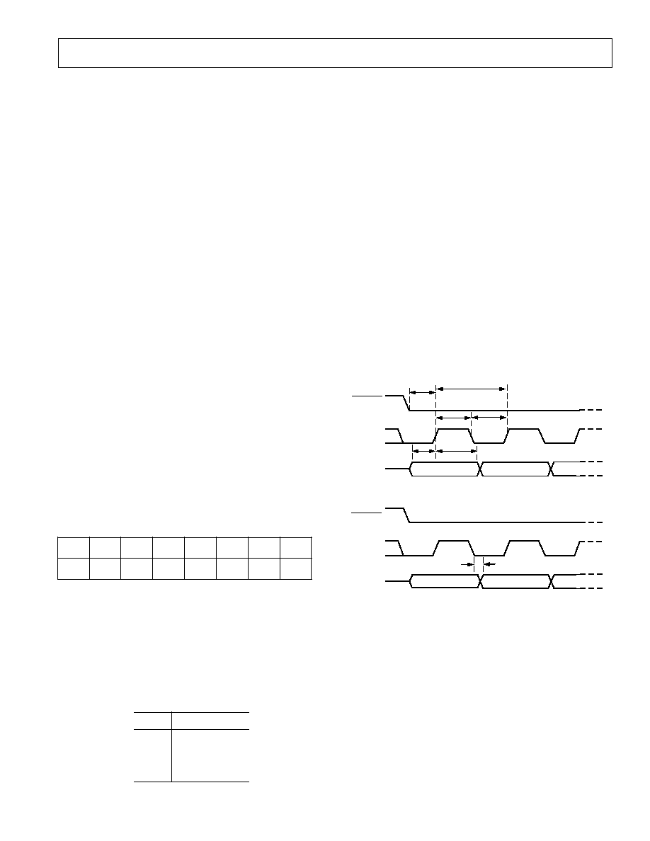
Transmit Port Timing
The AD9875 transmit port consists of a 6-bit data bus Tx[5:0],
a clock and a Tx SYNC signal. Two consecutive nibbles of the
Tx data are multiplexed together to form a 10-bit data word.
The clock appearing on the CLK-A pin is a buffered version of
the internal Tx data sampling clock. Data from the Tx port is
read on the rising edge of this sampling clock. The Tx SYNC
signal is used to indicate to which word a nibble belongs. The
first nibble of every word is read while Tx SYNC is low, the
second nibble of that same word is read on the following Tx
SYNC high level. The timing is illustrated in the Figure 5.
Tx2 LSB
Tx3 MSB
Tx1 LSB
Tx2 MSB
Tx0 LSB
Tx1 MSB
t
SU
t
HD
CLK-A
Tx SYNC
Tx [5:0]
Figure 5. Transmit Timing Diagram AD9875
The Tx port is highly configurable and offers the following
options:
Negative edge sampling can be chosen by two different methods;
either by setting the Tx Port Negative Edge Sampling bit (Register 3,
Bit 7) or the Invert CLK-A bit (Register 8, Bit 6). The main differ-
ence between the two methods is that setting Register 3, Bit 7
inverts the internal sampling clock and will affect only the transmit
path, even if CLK≠A is used to clock the Rx data. Inverting CLK-A
would affect both the Rx and Tx paths if they both use CLK-A.
The first nibble of each word can be read in as the least significant
nibble by setting the Tx LS Nibble First bit (Register 7, Bit 2).
For the AD9875, the most significant nibble defaults to six bits
and the least significant nibble defaults to form four bits. This
can be changed so that the least significant nibble and most
significant nibble have five bits each. This is done by setting the
Tx Port Width Five Bits bit (Register 7, Bit 1). In all cases, the
nibbles are justified toward Bit 5.
Also, the Tx path can be used in a reduced resolution mode by
setting the Tx Port Multiplexer Bypass bit (Register 7, Bit 0). In
this mode the Tx data word becomes six bits and is read in a
single cycle. The clocking modes are the same as described
above, but the level of Tx SYNC is irrelevant.
If Tx SYNC is low for more than one clock cycle, the last trans-
mit data will read continuously until Tx SYNC is brought high
for the second nibble of a new transmit word. This feature can
be used to "flush" the interpolator filters with zeros.
PGA Gain Adjust Timing
In addition to the serial port, the Tx[5:1] pins can be used to
write to the Rx Path Gain Adjust bits (Register 6, Bits 4:0). This
provides a faster way to update the PGA gain. A high level on
the GAIN pin with Tx SYNC low programs the PGA setting on
the rising edge of CLK-A. A low level on the GAIN pin enables
data to be fed to the interpolator and DAC. The GAIN pin
must be held high, the Tx SYNC must be held low, and
the GAIN data must be stable for three clock cycles to
successfully update the PGA GAIN value.
It should be noted that Tx SYNC must be held low and Tx
GAIN must be held high to update the gain register. If Tx
GAIN and Tx SYNC are both high, no data is written to the
gain register of the Tx data path.
Tx [5:0]
GAIN
GAIN
t
SU
CLK-A
Tx SYNC
t
HD
Figure 6. GAIN Programming
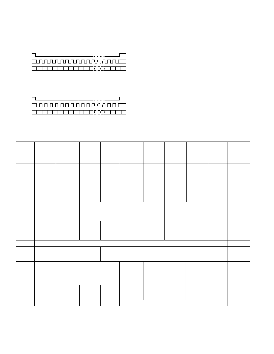
Receive Port Timing
The AD9875 receives port consists of a six bit data bus Rx[5:0],
a clock and an Rx SYNC signal. Two consecutive nibbles of the
Rx data are multiplexed together to form a 10-bit data word.
The Rx data is valid on the rising edge of CLK-A when the
ADC Clock Source PLL-B/2 bit (Register 3, Bit 6) is set to 0.
The Rx SYNC signal is used to indicate to which word a nibble
belongs. The first nibble of every word is transmitted while Rx
SYNC is low, the second nibble of that same word is transmit-
ted on the following Rx SYNC high level. When Rx SYNC is
low, the sampled nibble is read as the most significant nibble.
When the Rx SYNC is high, the sampled nibble is read as the
least significant nibble. The timing is illustrated in Figure 7.
t
VT
Rx2 LSB
Rx3 MSB
Rx1 LSB
Rx2 MSB
Rx0 LSB
Rx1 MSB
Rx [5:0]
t
HT
CLK-A (-B)
Rx SYNC
Figure 7. Receive Timing Diagram
The Rx port is highly configurable and offers the following
options:
Negative edge sampling can be chosen by setting the Invert
CLK-A bit (Register 8, Bit 6) or the Invert CLK-B bit (Register
8, Bit 7), depending on the clock selected as the ADC sampling
source. Inverting CLK-A would affect the Tx sampling edge as
well as the Rx sampling edge.
The first nibble of each word can be read in as the least signifi-
cant nibble by setting the Rx LS Nibble First bit (Register 8, Bit 2).
REV. 0
AD9875
≠19≠
Bits I4:I0 ≠ A4:A0
These bits determine which register is accessed during the data
transfer portion of the communications cycle. For multibyte
transfers, this address is the starting byte address. The remain-
ing register addresses are generated by the AD9875.
Serial Interface Port Pin Description
SCLK--Serial Clock
The serial clock pin is used to synchronize data transfers to and
from the AD9875 and to run the internal state machines. SCLK
maximum frequency is 25 MHz. All data transmitted to the
AD9875 is sampled on the rising edge of SCLK. All data read
from the AD9875 is validated on the rising edge of SCLK and is
updated on the falling edge.
SENABLE--Serial Interface Enable
The
SENABLE pin is active low. It enables the serial communi-
cation to the device.
SENABLE select should stay low during
the entire communication cycle. All input on the serial port is
ignored when
SENABLE is inactive.
SDATA--Serial Data I/O
The signal on this line is sampled on the first eight rising edges
of SCLK after
SENABLE goes active. Data is then read from or
written to the AD9875 depending on what was read.
Figures 8 and 9 show the timing relationships between the three
SPI signals.
SENABLE
SCLK
SDATA
t
DH
t
DS
t
DS
t
PWH
t
SCLK
t
PWL
INSTRUCTION BIT 7
INSTRUCTION BIT 6
Figure 8. Timing Diagram Register Write to AD9875/AD9876
SENABLE
SCLK
SDATA
DATA BIT n
DATA BIT n≠1
t
DV
Figure 9. Timing Diagram Register Read from AD9875/AD9876
MSB/LSB Transfers
The AD9875 serial port can support both most significant bit
(MSB) first or least significant bit (LSB) first data formats. The
bit order is controlled by the SPI LSB First bit (Register 0, Bit 6).
The default is value is 0, MSB first. Multibyte data transfers in
MSB format can be completed by writing an instruction byte
that includes the register address of the last address to be accessed.
The AD9875 will automatically decrement the address for each
successive byte required for the multibyte communication cycle.
When the SPI LSB First bit (Register 0, Bit 6) is set high, the
serial port interprets both instruction and data bytes LSB first.
Multibyte data transfers in LSB format can be completed by
writing an instruction byte that includes the register address of
the first address to be accessed. The AD9875 will automatically
increment the address for each successive byte required for the
multibyte communication cycle.
For the AD9875, the most significant nibble defaults to six bits
and the least significant nibble defaults to four bits. This can be
changed so that the least significant nibble and most significant
nibble have five bits each. This is done by setting the Rx Port
Width Five Bits bit (Register 8, Bit 1). In all cases, the nibbles
are justified toward Bit 5.
Also, the Rx path can be used in a reduced resolution mode by
setting the Rx Port Multiplexer Bypass bit (Register 8, Bit 0). In
this mode the Rx data word becomes six bits and is read in a
single cycle. The clocking modes are the same as described above,
but the level of Rx SYNC will stay low.
The Rx[5:0] pins can be put into a high impedance state by
setting the Three-State Rx Port bit (Register 8, Bit 3).
SERIAL INTERFACE FOR REGISTER CONTROL
The serial port is a three wire serial communications port consisting
of a clock (SCLK), chip select (
SENABLE), and a bidirectional
data (SDATA) signal. The interface allows read/write access to
all registers that configure the AD9875 internal parameters.
Single or multiple byte transfers are supported as well as MSB
first or LSB first transfer formats.
General Operation of the Serial Interface
Serial communication over the serial interface can be from 1 to
5 bytes in length. The first byte is always the instruction byte.
The instruction byte establishes whether the communication is
going to be a read or write access, the number of data bytes to
be transferred and the address of the first register to be accessed.
The instruction byte transfer is complete immediately upon the
eighth rising edge of SCLK after
SENABLE is asserted. Like-
wise, the data registers change immediately upon writing to the
eighth bit of each data byte.
Instruction Byte
The instruction byte contains the following information as
shown below:
Table II. Instruction Byte Information
B
S
M
B
S
L
7
I
6
I
5
I
4
I
3
I
2
I
1
I
0
I
W
/
R
1
N
0
N
4
A
3
A
2
A
1
A
0
A
Bit I7 ≠ R/W
This bit determines whether a read or a write data transfer will
occur after the instruction byte write. Logic high indicates read
operation; logic zero indicates a write operation.
Bits I6:I5 ≠ N1:N0
These two bits determine the number of bytes to be transferred
during the data transfer cycle. The bit decodes are shown in the
table below:
Table III. Decode Bits
N1:N0
Description
0:0
Transfer 1 Byte
0:1
Transfer 2 Bytes
1:0
Transfer 3 Bytes
1:1
Transfer 4 Bytes
REV. 0
AD9875
≠20≠
Figures 10a and 10b show how the serial port words are built
for each of these modes.
SENABLE
SCLK
SDATA
R/W I6
(N)
I5
(N)
I3
I4
I2
I1
I0
D7
N
D6
N
D2
0
D1
0
D0
0
INSTRUCTION CYCLE
DATA TRANSFER CYCLE
Figure 10a. Serial Register Interface Timing MSB-First
SENABLE
SCLK
SDATA
I0
I6
(N)
I5
(N)
I3
I4
I2
I1
R/W
D7
N
D6
N
D2
0
D1
0
D0
0
INSTRUCTION CYCLE
DATA TRANSFER CYCLE
Figure 10b. Serial Register Interface Timing LSB-First
Notes on Serial Port Operation
The serial port is disabled and all registers are set to their default
values during a hardware reset. During a software reset, all
registers except register 0 are set to their default values. Register
0 will remain at the last value sent, with the exception that the
Software Reset bit will be set to 0.
The serial port is operated by an internal state machine and is
dependent on the number of SCLK cycles since the last time
SENABLE went active. On every eighth rising edge of SCLK, a
byte is transferred over the SPI. During a multibyte write cycle,
this means the registers of the AD9875 are not simultaneously
updated, but occur sequentially. For this reason, it is recom-
mended that single byte transfers be used when changing the
SPI configuration or performing a software reset.
Table IV. Register Layout
Address
Default
(hex)
Bit 7
Bit 6
Bit 5
Bit 4
Bit 3
Bit 2
Bit 1
Bit 0
(hex)
Comments
0
SPI
Software
0
◊
00
Read/Write
LSB First
Reset
1
Power-
Power-
Power-
Power-
Power-
Power-
Power-
Power-
0
◊
00
Read/Write
Down
Down
Down
Down
Down
Down
Down
Down
PWR DN
Regulator
PLL-B
PLL-A
DAC
Interpolator
Rx
ADC and
Rx LPF and
Pin Low
Reference
FPGA
CPGA
2
Power-
Power-
Power-
Power-
Power-
Power-
Power-
Power-
0
◊
9F
Read/Write
Down
Down
Down
Down
Down
Down
Down
Down
PWR DN
Regulator
PLL-B
PLL-A
DAC
Interpolator
Rx
ADC and
Rx LPF and
Pin High
Reference
FPGA
CPGA
3
Tx Port
ADC Clock
PLL-B
PLL-B
PLL-A
0
◊
02
Read/Write
Negative
Source
(
◊
M) Multiplier
(
) Divider
(
◊
M) Multiplier
Edge
PLL-B/2
< 5:4>
< 3:3>
< 1:0>
Sampling
4
Tx Port
Rx LPF
Rx Path
Rx Digital Fast ADC
Wideband
Enable
Rx LPF
0
◊
01
Read/Write
Tuning
Tuning
DC Offset
HPF
Sampling
Rx LPF
1-Pole
Bypass
Update
In Progress
Correction Bypass
Rx LPF
Disable
(Read Only)
5
Rx LPF Fc Adjust <4:0>
0
◊
80
Read/Write
6
PGA
Rx Path Gain Adjust <4:0>
0
◊
00
Read/Write
Gain Set
by Register
7
Interpolation Filter Select
Power-Down
Tx Port
Tx Port
Tx Port
0
◊
00
Read/Write
<3:0>
Interpolator
LS Nibble
Width
Multiplexer
at
First
5-bits
Bypass
Tx QUIET
Pin Low
8
Invert
Invert
Invert
Invert
Three-State
Rx Port
Rx Port
Rx Port
0
◊
00
Read/ Write
CLK B
CLK B
CLK B
CLK B
Rx Port
LS Nibble
Width
Multiplexer
First
5-bits
Bypass
F
Die Revision Number <3:0>
Read Only

REV. 0
AD9875
≠21≠
REGISTER PROGRAMMING DEFINITIONS
REGISTER 0--RESET/SPI Configuration
Bit 5: Software Reset
Setting this bit high resets the chip. The PLLs will relock to the
input clock and all registers (except Register 0
◊
0, Bit 6) revert
to their default values. Upon completion of the reset, Bit 5 is
reset to 0.
The content of the interpolator stages are not cleared by software
or hardware resets. It is recommended to "flush" the transmit
path with zeros before transmitting data.
Bit 6: LSB/MSB First
Setting this bit high causes the serial port to send and receive
data least significant bit (LSB) first. The default low state con-
figures the serial port to send and receive data most significant
bit (MSB) first.
REGISTERS 1 and 2--Power-Down
The combination of the PWR DN pin and Registers 1 and 2
allow for the configuration of two separate pin selectable power
settings. The PWR DN pin selects between two sets of individu-
ally programmed operation modes.
When the PWR DN pin is low, the functional blocks corre-
sponding to the bits set in register 1 will be powered down.
When the PWR DN pin is high, the functional blocks corre-
sponding to the bits set in Register 2 will be powered down
Bit 0: Power-Down Receive Filter and CPGA
Setting this bit high powers down and bypasses the Rx LPF and
coarse programmable gain amplifier.
Bit 1: Power-Down ADC and FPGA
Setting this bit high powers down the ADC and fine program-
mable gain amplifier (FPGA).
Bit 2: Power-Down Rx Reference
Setting this bit high powers down the ADC reference. This bit
should be set if an external reference is applied.
Bit 3: Power-Down Interpolators
Setting this bit high powers down the transmit digital interpola-
tors. It does not clear the content of the data path.
Bit 4: Power-Down DAC
Setting this bit high powers down the transmit DAC.
Bit 5, Bit 6: Power-Down PLL-A, PLL-B
Setting these bits high powers down the on-chip phase lock
loops which generated CLK-A and CLK-B respectively. When
powered down these clocks are high impedance.
Bit 7: Power-Down Regulator
Setting this bit high powers down the on-chip voltage control regulator.
REGISTER 3--CLOCK SOURCE CONFIGURATION
The AD9875 integrates two independently programmable PLLs
referred to as PLL-A and PLL-B. The output of the PLLs are
used to generate all the chips internal and external clock signals
from the f
CLKIN
signal. All Tx path clock signals are derived
from PLL-A. If f
CLKIN
is programmed as the ADC sampling
clock source, the Rx port clocks are also derived from PLL-A.
Otherwise, the ADC sampling clock is PLL-B/2 and the Rx path
clocks are derived from PLL-B.
Bit 1,0: PLL-A Multiplier
Bits 1 and 0 determine the multiplication factor (L) for PLL-A
and the DAC sampling clock frequency, f
DAC.
f
DAC
= L
◊
f
CLKIN
Bit 1,0
0,0: L = 1
0,1: L = 2
1,0: L = 4
1,1: L = 8
Bit 5 to 2: PLL-B Multiplier/Divider
Bits 5 to 2 determine the multiplication factor (M) and division
factor (N) for PLL-B and the CLK-B frequency. For multiplexed
10-/12-bit data, f
CLK-B
= f
CLKIN
◊
M/N. For nonmultiplexed 6-bit
data, f
CLK-B
= (f
CLKIN
/2)
◊
M/N. All nine combinations of M and N
values are valid, yielding seven unique M/N ratios.
Bit 5,4
Bit 3,2
0,0: M = 3
0,0: N = 2
0,1: M = 4
0,1: N = 4
1,0: M = 6
1,0: N = 1
Bit 6: ADC Clock Source PLL-B/2
Setting Bit 6 high selects PLL-B/2 as the ADC sampling Clock
source. In this mode, the Rx data and CLK-B will run at a rate
of f
CLK-B
. RxSYNC will run at f
CLK-B
/2.
Setting Bit 6 low selects the f
CLKIN
signal as the ADC sampling
clock source. This mode of operation yields the best ADC
performance if an external crystal is used or a low jitter clock
source drives the OSCIN pin.
Bit 7: Tx Port Negative Edge Sampling
Setting Bit 7 high will cause the Tx port to sample the TxDATA
and TxSYNC on the falling edge of CLK-A. By default, the Tx
Port sampling occurs on the rising edge of CLK-A. The timing
is shown in Figure 5.
REGISTER 4--RECEIVE FILTER SELECTION
The AD9875 receive path has a continuous time 4-pole LPF
and a 1-pole digital HPF. The 4-pole LPF has two selectable
cutoff frequencies. Additionally, the filter can be tuned around
those two cutoff frequencies. These filters can also be bypassed
to different degrees as described below.
The continuous time 4-pole low-pass filter is automatically
calibrated to one of two selectable cutoff frequencies.
The cutoff frequency f
CUTOFF
is described as a function of the
ADC sampling frequency f
ADC
and can be influenced (
±
30%) by
the Rx-Filter Tuning Target word in Register 5.
f
CUTOFF LOW
= f
ADC
◊
64/(Target + 64)
f
CUTOFF HIGH
= f
ADC
◊
158/(Target + 64)
Bit 0: Rx LPF Bypass
Setting this bit high bypasses the 4-pole LPF. The filter is
automatically powered down when this bit is set.
Bit 1: Enable 1-Pole Rx LPF
The AD9875 can be configured with an additional 1-pole ~16 MHz
input filter for applications that require steeper filter roll-off or
want to use the 1-pole filter instead of the 4-pole receive
Low-Pass filter. The 1-pole filter is untrimmed and subject to
cutoff frequency variations of
±
20%.
REV. 0
AD9875
≠22≠
Table V. PGA Programming Map
Rx Path
Rx Path
CPGA
SPGA
Gain [4:0]
Gain
Gain
Gain
0
◊
00
≠6
≠6
0
0
◊
01
≠4
≠6
2
0
◊
02
≠2
≠6
4
0
◊
03
0
≠6
6
0
◊
04
2
≠6
8
0
◊
05
4
≠6
10
0
◊
06
6
0
6
0
◊
07
8
0
8
0
◊
08
10
0
10
0
◊
09
12
6
6
0
◊
0A
14
6
8
0
◊
0B
16
6
10
0
◊
0C
18
12
6
0
◊
0D
20
12
8
0
◊
0E
22
12
10
0
◊
0F
24
18
6
0
◊
10
26
18
8
0
◊
11
28
18
10
0
◊
12
*
30/30
18/24
12/6
0
◊
13
*
30/32
18/24
12/8
0
◊
14
*
30/34
18/24
12/10
0
◊
15*
30/36
18/24
12/12
*When the Wideband Rx Filter bit is set high, the Rx Path Gain is limited to
30 dB. The first of the two values in the chart refers to this mode. The second
number refers to the mode when the lower Rx LPF cutoff frequency is chosen,
or the Rx LPF filter is bypassed.
REGISTER 7--TRANSMIT PATH SETTINGS
The AD9875 transmit path has a programmable interpolation
filter that precedes the transmit DAC. The interpolation filter
can be programmed to operate in seven different modes. Also,
the digital interface can be programmed to operate in several
different modes. These modes are described below.
Bit 0: Transmit Port Demultiplexer Bypass
Setting Bit 0 high bypasses the input data demultiplexer. In this
mode, consecutive nibbles on the TxDATA(5:0) pins are treated
as individual words to be sent through the Tx path. This creates
a six bit data path. The state of TxSYNC is ignored in this mode.
Bit 1: Transmit Port Width
If Bit 1 is set high, the Tx port will operate such that the most
significant nibble and the least significant nibble are each five
bits wide. The default mode is six bits for the most significant
nibble and four bit for the least significant nibble. The data is
always aligned to the MSB pin Tx[5]. Enabling this pin on the
AD9875 allows for a five pin versus the default six pin interface.
Bit 2: Transmit Port Least Significant Nibble First
Setting Bit 2 high reconfigures the AD9875 for a transmit
mode that expects least significant nibble before the most
significant nibble.
Bit 2: Wideband Rx LPF
This bit selects the nominal cutoff frequency of the 4-pole LPF.
Setting this bit high selects a nominal cutoff frequency of 28.8 MHz.
When the wideband filter is selected, the Rx path gain is limited
to 30 dB.
Bit 3: Fast ADC Sampling
Setting this bit increases the quiescent current in the SVGA
block. This may provide some performance improvement
when the ADC sampling frequency is greater than 50 MSPS
(in 6-bit mode).
Bit 4: Rx Digital HPF Bypass
Setting this bit high bypasses the 1-pole digital HPF that follows
the ADC. The digital filter must be bypassed for ADC sampling
above 50 MSPS.
Bit 5: Rx Path DC Offset Correction
Writing a One to this bit triggers an immediate receive path
offset correction and reads back zero after the completion of the
offset correction.
Bit 6: Rx LPF Tuning Update In Progress
This bit indicates when receive filter calibration is in progress.
The duration of a receive filter calibration is about 500 ms.
Writing to this bit has no effect.
Bit 7: Rx LPF Tuning Update Disable
Setting this bit high disables the automatic background receive
filter calibration. The AD9875 automatically calibrates the
receive filter on reset and every few (~2) seconds thereafter to
compensate for process and temperature variation, power supply
and long term drift. Programming a one to this bit disables this
function. Programming a zero triggers an immediate first cali-
bration and enables the periodic update.
REGISTER 5--RECEIVE FILTER TUNING TARGET
This register sets the filter tuning target as a function of f
OSCIN
.
See Register 4 description.
REGISTER 6--Rx PATH GAIN ADJUST
The AD9875 uses a combination of a continuous time PGA
(CPGA) and a switched capacitor PGA (SPGA) for a gain range
of ≠6 to 36 dB with a resolution of 2 dB. The Rx path gain can
be programmed over the serial interface by writing to the Rx
Path Gain Adjust register or directly using the GAIN and MSB
aligned Tx[5:1] bits. The register default value is 0
◊
00 for
lowest gain setting (≠6 dB). The register always reads back the
actual gain setting irrespective of which of the two programming
modes were used.
Table V describes the gains and how they are achieved as a
function of the Rx Path adjust bits.
Bit 5: PGA Gain Set through Register
Setting this bit high will result in the Rx Path Gain being set by
writing to the PGA Gain Control register. Default is zero which
selects writing the gain through the Tx[5:1] pins in conjunction
with the gain pin.

REV. 0
AD9875
≠23≠
Bit 3: Power-Down Interpolator at TxQUIET Pin Low
Setting Bit 3 high enables the TxQUIET pin to shut off the
DAC output. If the bit is set to one, then pulling the TxQUIET
pin low will power down the interpolator filters. In most appli-
cations the interpolator filter will need to be flushed with zeros
before or after being powered down.
Bit 4 to Bit 7: Interpolation Filter Select
Bits 4 to 7 define the Interpolation filter characteristic and inter-
polation rate.
Bits 7:4;
0
◊
2; Interpolation Bypass.
0
◊
0; see TPC 1. 4
◊
Interp, LPF.
0
◊
1; see TPC 2. 2
◊
Interp, LPF.
0
◊
4; see TPC 3. 4
◊
Interp, BPF, Adj image.
0
◊
5; see TPC 4. 2
◊
Interp, BPF, Adj image.
0
◊
8; see TPC 5. 4
◊
Interp, BPF, lower image.
0
◊
C; see TPC 6. 4
◊
Interp, BPF, upper image.
The interpolation factor has a direct influence on the CLK-A
output frequency. When the transmit input data multiplexer is
enabled (10-bit mode):
f
CLK-A
= 2
◊
f
DAC
/K
where K is the interpolation factor.
When the transmit input data multiplexer is disabled (5-/6-bit
mode):
f
CLK-A
= f
DAC
/K
where K is the interpolation factor.
REGISTER 8--RECEIVER AND CLOCK OUTPUT
SETTINGS
Bit 0: Rx Port Multiplexer Bypass
Setting this bit high bypasses the Rx port output multiplexer.
This will output only the 6 MSBs of the ADC word. This mode
enables ADC sampling rates above 55 MSPS.
Bit 1: Rx Port Width Five Bits
If the bit is set high, the Rx port data will be output in two
nibbles of five bits each (on pins Rx[5:1]). When this bit is low
(default), the most significant nibble will contain six bits and the
least significant nibble will have four bits. The default mode
makes the AD9875 pin compatible with the AD9876.
Bit 2: Rx Port LS Nibble First
Reconfigures the AD9875 for a receive mode that expects less
significant bits before the most significant bits.
Bit 3: Three-State Rx Port
This bit sets the receive output Rx[5:0] into a high impedance
three-state mode. It allows for sharing the bus with other devices.
Bit 4, Bit 5: Disable CLK-A, Disable CLK-B
Setting Bit 4 or Bit 5 stops CLK-A or CLK-B respectively, from
toggling. The output is held to a logic 0 level.
Bit 4, Bit 5: Disable CLK-A, Disable CLK-B
Setting Bit 4 or Bit 5 fixes CLK-A or CLK-B to a low output
level, respectively.
Bit 6: CLK-A Output Invert
Setting Bit 6 high inverts the CLK-A output signal.
Bit 7: CLK-B Output Invert
Setting this bit high inverts the CLK-B output signal. This effec-
tively changes the timing of the Rx[5:0] and RxSYNC signals from
rising edge triggered to falling edge triggered with respect to the
CLK-B signal.
REGISTER F, DIE REVISION
This register stores the die revision of the chip. It is a read-
only register.
PCB DESIGN CONSIDERATIONS
Although the AD9875 is a mixed-signal device, the part should
be treated as an analog component. The digital circuitry on-chip
has been specially designed to minimize the impact that the
digital switching noise will have on the operation of the analog
circuits. Following the power, grounding and layout recommen-
dations in this section will help you get the best performance
from the MxFE.
Component Placement
If the three following guidelines of component placement are
followed, chances for getting the best performance from the
MxFE
are greatly increased. First, manage the path of return
currents flowing in the ground plane so that high frequency
switching currents from the digital circuits do not flow on the
ground plane under the MxFE or analog circuits. Second, keep
noisy digital signal paths and sensitive receive signal paths as
short as possible. Third, keep digital (noise generating) and
analog (noise susceptible) circuits as far away from each other
as possible.
In order to best manage the return currents, pure digital circuits
that generate high switching currents should be closest to the
power supply entry. This will keep the highest frequency return
current paths short, and prevent them from traveling over the
sensitive MxFE and analog portions of the ground plane. Also,
these circuits should be generously bypassed at each device
which will further reduce the high frequency ground currents.
The MxFE should be placed adjacent to the digital circuits,
such that the ground return currents from the digital sections
will not flow in the ground plane under the MxFE. The analog
circuits should be placed furthest from the power supply.
The AD9875 has several pins which are used to decouple sensi-
tive internal nodes. These pins are REFIO, REFB, and REFT.
The decoupling capacitors connected to these points should
have low ESR and ESL. These capacitors should be placed as
close to the MxFE as possible and be connected directly to the
analog ground plane.
The resistor connected to the FSADJ pin should also be placed
close to the device and connected directly to the analog ground plane.
Power Planes and Decoupling
The AD9875 evaluation board demonstrates a good power supply
distribution and decoupling strategy. The board has four layers;
two signal layers, one ground plane and one power plane. The
power plane is split into a 3VDD section used for the 3 V digital
logic circuits, a DVDD section used to supply the digital supply
pins of the AD9875, an AVDD section used to supply the
analog supply pins of the AD9875, and a VANLG section that
supplies the higher voltage analog components on the board.
The 3VDD section will typically have the highest frequency
currents on the power plane and should be kept the furthest
from the MxFE and analog sections of the board. The DVDD
portion of the plane brings the current used to power the digital
portion of the MxFE to the device. This should be treated
similarly to the 3VDD power plane and be kept from going
underneath the MxFE or analog components. The MxFE
should largely sit on the AVDD portion of the power plane.

≠24≠
C02488≠1≠7/01(0)
PRINTED IN U.S.A.
REV. 0
The AVDD and DVDD power planes may be fed from the same
low noise voltage source; however, they should be decoupled
from each other to prevent the noise generated in the DVDD
portion of the MxFE from corrupting the AVDD supply. This
can be done by using ferrite beads between the voltage source
and DVDD, and between the source and AVDD. Both DVDD
and AVDD should have a low ESR, bulk decoupling capacitor
on the MxFE side of the ferrite as well as a low ESR, ESL
decoupling capacitors on each supply pin (i.e., the AD9875
requires five power supply decoupling caps, one each on Pins 5,
38, 47, 14, and 35). The decoupling caps should be placed as close
to the MxFE supply pins as possible. An example of the proper
decoupling is shown in the AD9875 evaluation board schematic.
Ground Planes
In general, if the component placing guidelines discussed earlier
can be implemented, it is best to have at least one continuous
ground plane for the entire board. All ground connections should be
made as short as possible. This will result in the lowest impedance
return paths, and the quietest ground connections.
If the components cannot be placed in a manner that will keep
the high-frequency ground currents from traversing under the
MxFE and analog components, it may be necessary to put
current steering channels into the ground plane to route the
high-frequency currents around these sensitive areas. These current
steering channels should be made only when and where necessary.
Signal Routing
The digital Rx and Tx signal paths should be kept as short as
possible. Also, the impedance of these traces should have a
controlled characteristic impedance of about 50
. This will
prevent poor signal integrity and the high currents that can
occur during undershoot or overshoot caused by ringing. If the
signal traces cannot be kept shorter than about 1.5 inches, then
series-termination resistors (33
to 47
) should be placed
close to all signal sources. It is a good idea to series-terminate all
clock signals at their source, regardless of trace length.
The receive Rx
±
signals are the most sensitive signals on the
entire board. Careful routing of these signals is essential for good
receive path performance. The Rx
±
signals form a differential pair
and should be routed together as a pair. By keeping the traces
adjacent to each other, noise coupled onto the signals will
appear as common-mode and will be largely rejected by the
MxFE receive input. Keeping the driving point impedance of
the receive signal low and placing any low-pass filtering of the
signals close to the MxFE will further reduce the possibility of
noise corrupting these signals.
OUTLINE DIMENSIONS
AD9875
Dimensions shown in inches and (mm).
48-Lead LQFP
(ST-48)
0.039 (1.00)
REF
TOP VIEW
(PINS DOWN)
1
12
13
25
24
36
37
48
0.011 (0.27)
0.009 (0.22)
0.007 (0.17)
0.019 (0.50)
BSC
0.276
(7.00)
BSC
SQ
0.354 (9.00)
BSC SQ
SEATING
PLANE
0.063 (1.60)
MAX
0.030 (0.75)
0.024 (0.60)
0.018 (0.45)
VIEW A
7
3.5
0
0.008 (0.20)
0.004 (0.09)
0.057 (1.45)
0.055 (1.40)
0.053 (1.35)
0.006 (0.15)
0.002 (0.05)
0.003 (0.08)
MAX
VIEW A
ROTATED 90 CCW
CONTROLLING DIMENSIONS ARE IN MILLIMETERS.