 | –≠–ª–µ–∫—Ç—Ä–æ–Ω–Ω—ã–π –∫–æ–º–ø–æ–Ω–µ–Ω—Ç: AD9877 | –°–∫–∞—á–∞—Ç—å:  PDF PDF  ZIP ZIP |
Document Outline
- ˛ˇ
- ˛ˇ
- ˛ˇ
- ˛ˇ
- ˛ˇ
- ˛ˇ
- ˛ˇ
- ˛ˇ
- ˛ˇ
- ˛ˇ
- ˛ˇ
- ˛ˇ
- ˛ˇ
- ˛ˇ
- ˛ˇ
- ˛ˇ
- ˛ˇ
- ˛ˇ
- ˛ˇ
- ˛ˇ
- ˛ˇ
- ˛ˇ
- ˛ˇ
- ˛ˇ
- ˛ˇ
- ˛ˇ
- ˛ˇ
- COMBINED FILTER RESPONSE
- ˛ˇ
- ˛ˇ
- ˛ˇ
- ˛ˇ
- ˛ˇ
- ˛ˇ
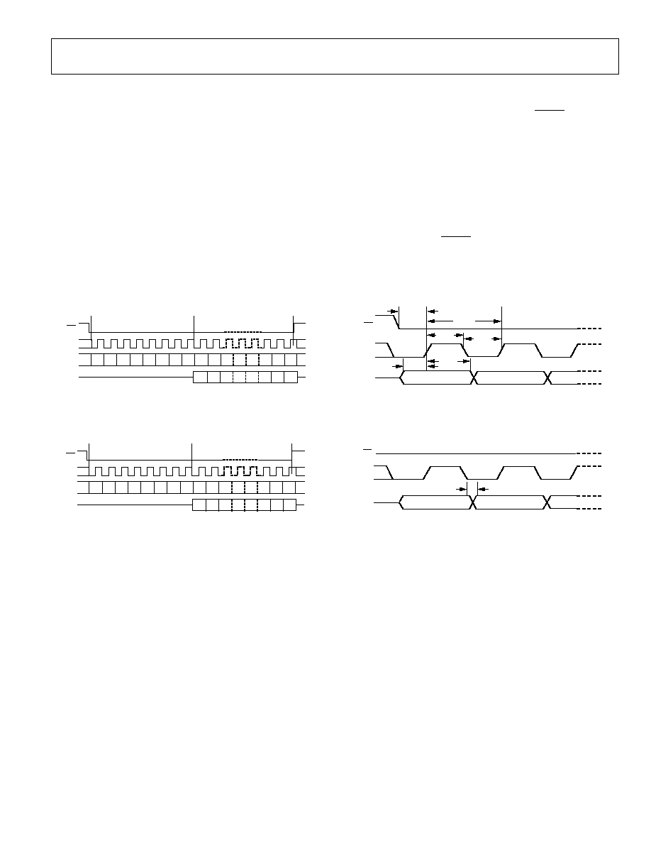
- RECEIVE TIMING
- ˛ˇ
- ˛ˇ
- ˛ˇ
- ADC VOLTAGE REFERENCES
- ˛ˇ
- ˛ˇ
- POWER PLANES AND DECOUPLING
- ˛ˇ
- SIGNAL ROUTING
- ˛ˇ
Mixed-Signal Front End
Set-Top Box, Cable Modem
AD9877
Rev. B
Information furnished by Analog Devices is believed to be accurate and reliable.
However, no responsibility is assumed by Analog Devices for its use, nor for any
infringements of patents or other rights of third parties that may result from its use.
Specifications subject to change without notice. No license is granted by implication
or otherwise under any patent or patent rights of Analog Devices. Trademarks and
registered trademarks are the property of their respective owners.
One Technology Way, P.O. Box 9106, Norwood, MA 02062-9106, U.S.A.
Tel: 781.329.4700
www.analog.com
Fax: 781.461.3113
© 2005 Analog Devices, Inc. All rights reserved.
FEATURES
Low cost 3.3 V CMOS MxFETM for
MCNS-DOCSIS-, DVB-, DAVIC-compliant
set-top box and cable modem applications
232 MHz quadrature digital upconverter
12-bit direct IF DAC (TxDAC+Æ)
Up to 65 MHz carrier frequency DDS
Programmable sampling clock rates
Selectable interpolation filter
Analog Tx output level adjust
12-bit, 33 MSPS direct IF ADC
Dual 8-bit, 16.5 MSPS sampling IQ ADCs
Two 12-bit - auxiliary DACs
Direct interface to AD8321/AD8325 or
AD8322/AD8327 PGA cable driver
APPLICATIONS
Cable modems
Set-top boxes
Wireless modems
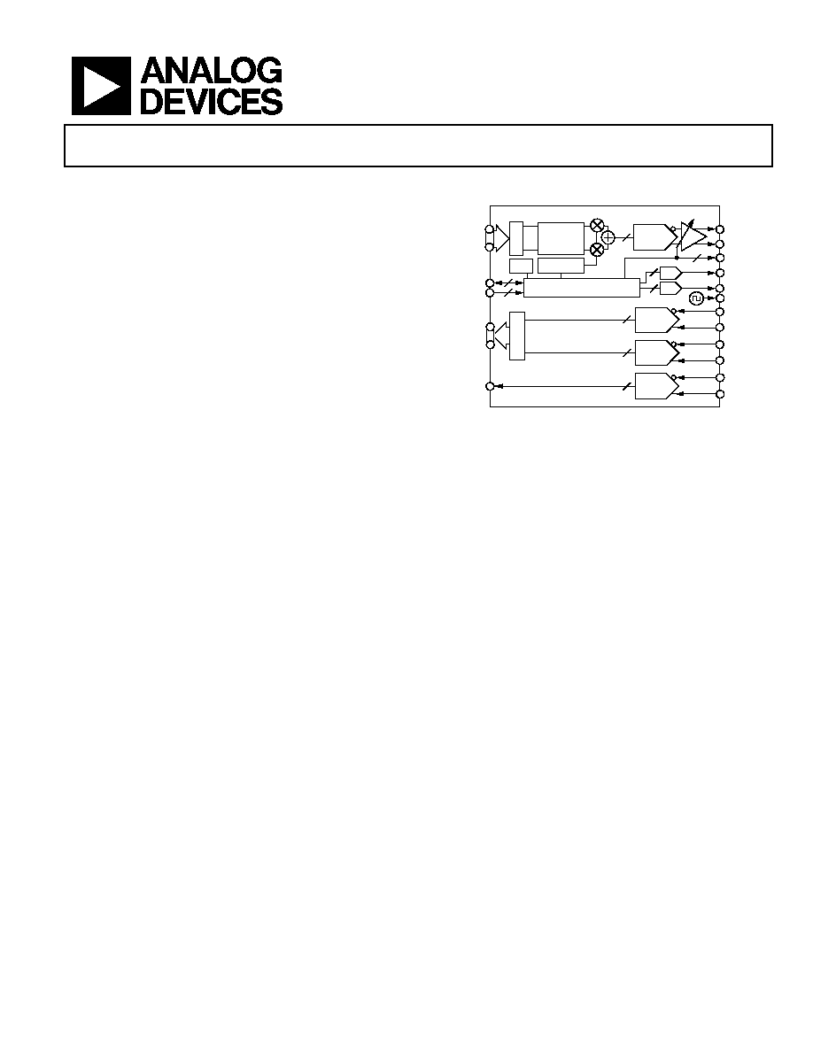
FUNCTIONAL BLOCK DIAGRAM
ADC
12
12
DAC
12
12
SDELTA0
SDELTA1
DDS
COS
SIN
INTER-
POLATOR
FILTER
Tx
CONTROL FUNCTIONS
Rx
PLL
REFCLK
I IN
Q IN
CA
Tx
IF IN
Tx DATA
SPORT
PROFILE
RxIQ DATA
4
2
3
RxIF DATA
ADC
8
ADC
8
-
-
AD9877
02716-001
Figure 1.
GENERAL DESCRIPTION
The AD9877 is a single-supply set-top box and cable modem
mixed-signal front end. The device contains a transmit path
interpolation filter, complete quadrature digital upconverter,
and transmit DAC. The receive path contains a 12-bit ADC and
dual 8-bit ADCs. All internally required clocks and an output
system clock are generated by the phase-locked loop (PLL) from
a single crystal or clock input.
The transmit path interpolation filter provides upsampling
factors of 12◊ or 16◊ with an output signal bandwidth as high
as 5.8 MHz. Carrier frequencies up to 65 MHz with 26 bits of
frequency tuning resolution can be generated by the direct
digital synthesizer (DDS). The transmit DAC resolution is 12 bits
and can run at sampling rates as high as 232 MSPS. Analog
output scaling from 0 dB to 7.5 dB in 0.5 dB steps is available to
preserve SNR when reduced output levels are required.
The 12-bit ADC has excellent undersampling performance,
allowing it to typically deliver better than 10 ENOBs with IF
inputs up to 70 MHz. The 12-bit IF ADC can sample at a rate
up to 33 MHz, allowing it to process wideband signal inputs.
Two programmable - DACs are available and can be used to
control external components, such as variable gain amplifiers
(VGAs) or voltage-controlled tuners.
The AD9877 integrates a CA port that enables a host processor
to control the AD8321/AD8325 or AD8322/AD8327
programmable gain amplifier (PGA) cable drivers via the
MxFE SPORT.
The AD9877 is available in a 100-lead MQFP package. It offers
enhanced receive path undersampling performance and lower
cost compared to the pin-compatible AD9873. The AD9877 is
specified over the extended industrial (-40∞C to +85∞C)
temperature range.

AD9877
Rev. B | Page 2 of 36
TABLE OF CONTENTS
Specifications..................................................................................... 4
Absolute Maximum Ratings............................................................ 7
Explanation of Test Levels ........................................................... 7
Thermal Characteristics .............................................................. 7
ESD Caution.................................................................................. 7
Pin Configuration and Function Descriptions............................. 8
Typical Performance Characteristics ........................................... 10
Terminology .................................................................................... 12
Theory of Operation ...................................................................... 13
Transmit Section......................................................................... 13
Clock and Oscillator Circuitry ................................................. 14
Programmable Clock Output REFCLK................................... 15
Reset and Transmit Power-Down ............................................ 16
- Outputs ................................................................................ 17
Register Map and Bit Definitions ................................................. 18
Register 0x00--Initialization .................................................... 19
Register 0x01--Clock Configuration....................................... 19
Register 0x02--Power-Down.................................................... 19
Register 0x03≠0x06--- Control Words.............................. 19
Register 0x08--ADC Clock Configuration ............................ 20
Register 0x0C--Die Revision.................................................... 20
Register 0x0D--Tx Frequency Tuning Words LSBs.............. 20
Register 0x0E--DAC Gain Control ......................................... 20
Register 0x0F--Tx Path Configuration ................................... 20
Registers 0x10≠0x1F--Burst Parameter .................................. 20
Serial Interface for Register Control ............................................ 22
General Operation of the Serial Interface ............................... 22
Instruction Byte .......................................................................... 22
Serial Interface Port Pin Description....................................... 22
MSB/LSB Transfers .................................................................... 22
Notes on Serial Port Operation ................................................ 23
Transmit Path (Tx) ......................................................................... 24
Transmit Timing......................................................................... 24
Data Assembler........................................................................... 24
Half-Band Filters (HBFs) .......................................................... 24
Cascaded Integrator-Comb (CIC) Filter................................. 24
Combined Filter Response........................................................ 25
Tx Signal Level Considerations ................................................ 27
Tx Throughput and Latency ..................................................... 27
Digital-to-Analog Converter .................................................... 27
Programming the AD8321/AD8325 or AD8322/AD8327 Cable
Driver Amplifier Gain Control..................................................... 29
Receive Path (Rx) ........................................................................... 30
ADC Theory of Operation........................................................ 30
Receive Timing ........................................................................... 30
Driving the Analog Inputs ........................................................ 30
Op Amp Selection Guide .......................................................... 31
ADC Differential Inputs............................................................ 31
ADC Voltage References ........................................................... 32
PCB Design Considerations.......................................................... 33
Component Placement .............................................................. 33
Power Planes and Decoupling .................................................. 33
Ground Planes ............................................................................ 33
Signal Routing............................................................................. 34
Outline Dimensions ....................................................................... 35
Ordering Guide .......................................................................... 35

AD9877
Rev. B | Page 3 of 36
REVISION HISTORY
5/05--Rev. A to Rev. B
Updated Format.................................................................. Universal
Changed OSCOUT to REFCLK....................................... Universal
Changed REF CLK to REFCLK........................................ Universal
Changes to Specifications.................................................................4
Changes to Figure 24 ......................................................................23
Updated Outline Dimensions........................................................35
Changes to Ordering Guide...........................................................35
7/02--Rev. 0 to Rev. A
Edits to ORDERING GUIDE ..........................................................5
Edits to RESET AND TRANSMIT POWER-DOWN section..17
Revision 0: Initial Version

AD9877
Rev. B | Page 4 of 36
SPECIFICATIONS
V
AS
= 3.3 V ± 5%, V
DS
= 3.3 V ± 10%, f
OSCIN
= 27 MHz, f
SYSCLK
= 216 MHz, f
MCLK
= 54 MHz (M = 8 and N = 4). ADC sample frequencies
derived from PLL (f
MCLK
), R
SET
= 4.02 k, maximum fine gain, 75 DAC load.
Table 1.
Parameter Temp
Test
Level
Min Typ
Max
Unit
SYSTEM CLOCK DAC SAMPLING, f
SYSCLK
Frequency Range (N = 4)
Full
II
232
MHz
Frequency Range (N = 3)
Full
II
177
MHz
OSCIN and XTAL CHARACTERISTICS
Frequency Range
Full
II
3
33
MHz
Duty Cycle
25∞C
II
35
50
65
%
Input Impedance
25∞C
III
100||3
M||pF
MCLK JITTER
Cycle to Cycle (f
MCLK
derived from PLL)
25∞C
III
6
ps rms
Tx DAC CHARACTERISTICS
Resolution N/A
N/A
12
Bits
Full-Scale Output Current
Full
II
4
10
20
mA
Gain Error (using internal reference)
Full
I
-2.5
-1
+2.5
% FS
Offset Error
25∞C
I
±1.0
% FS
Reference Voltage (REFIO Level)
25∞C
I
1.18
1.23
1.28
V
Differential Nonlinearity (DNL)
25∞C
III
±2.5
LSB
Integral Nonlinearity (INL)
25∞C
III
±8
LSB
Output Capacitance
25∞C
III
5
pF
Phase Noise @ 1 kHz Offset, 42 MHz Carrier
25∞C
III
-110
dBc/Hz
Output Voltage Compliance Range
Full
II
-0.5
+1.5
V
Wideband SFDR
5 MHz Analog Out, I
OUT
= 10 mA
Full
II
48
55
dBc
65 MHz Analog Out, I
OUT
= 10 mA
Full
II
48
51
dBc
Narrow-Band SFDR (±1 MHz Window)
65 MHz Analog Out, I
OUT
= 10 mA
Full
II
53
69
dBc
Tx MODULATOR CHARACTERISTICS
I/Q Offset
Full
II
50
55
dB
Pass-Band Amplitude Ripple (f < f
IQCLK
/8) Full
II
±0.1
dB
Pass-Band Amplitude Ripple (f < f
IQCLK
/4) Full
II
±0.5
dB
Stop-Band Response (f > f
IQCLK
◊ 3/4)
Full
II
-63
dB
Tx GAIN CONTROL
Gain Step Size
25∞C
III
0.5
dB
Gain Step Error
25∞C
III
0.05
dB
Settling Time, 1% (Full-Scale Step)
25∞C
III
1.8
s
8-BIT ADC CHARACTERISTICS
Resolution N/A
N/A
8
Bits
Conversion Rate
Full
II
16.5
MHz
Pipeline Delay
N/A
N/A
3.5
ADC cycles
Offset Matching Between I and Q ADCs
±8.0
LSBs
Gain Matching Between I and Q ADCs
±2.0
LSBs
Analog Input
Input Voltage Range
Full
II
1
Vppd
Differential Input Impedance
25∞C
III
4||2
k||pF
Full Power Bandwidth
25∞C
III
90
MHz
Input Referred Noise
25∞C
III
600
V

AD9877
Rev. B | Page 5 of 36
Parameter Temp
Test
Level Min
Typ Max
Unit
Dynamic Performance (A
IN
= -0.5 dBFS, f = 5 MHz)
Signal-to-Noise and Distortion (SINAD)
25∞C
I
40.8
47.3
dB
Effective Number of Bits (ENOB)
25∞C
I
6.5
7.6
Bits
Total Harmonic Distortion (THD)
25∞C
I
-60.1
-50.0
dB
Spurious-Free Dynamic Range (SFDR)
25∞C
I
52.0
63.0
dB
Reference Voltage Error
REFT8 to REFB8 (0.5 V)
25∞C
I
-100
±10
+100
mV
12-BIT ADC CHARACTERISTICS
Resolution N/A
N/A
12
Bits
Conversion Rate
Full
II
33
MHz
Pipeline Delay
N/A
N/A
5.5
ADC cycles
Analog Input
Input Voltage Range
Full
III
2
Vppd
Differential Input Impedance
25∞C
III
4||2
k||pF
Aperture Delay
25∞C
III
2.0
ns
Aperture Uncertainty (Jitter)
25∞C
III
1.2
ps rms
Full-Power Bandwidth
25∞C
III
85
MHz
Input Referred Noise
25∞C
III
75
V
Reference Voltage Error
REFT12 to REFB12 (1 V)
25∞C
I
-200
±16
±200
mV
Dynamic Performance (A
IN
= -0.5 dBFS, f = 5 MHz)
ADC Sample Clock = OSCIN
Signal-to-Noise and Distortion (SINAD)
Full
II
63.2
65.9
dB
Effective Number of Bits (ENOBs)
Full
II
10.2
10.7
Bits
Signal-to-Noise Ratio (SNR)
Full
II
63.7
66.2
dB
Total Harmonic Distortion (THD)
Full
II
-79.1
-68.3
dB
Spurious-Free Dynamic Range (SFDR)
Full
II
72.5
79.3
dB
ADC Sample Clock = PLL
Signal-to-Noise and Distortion (SINAD)
Full
II
62.0
64.6
dB
Effective Number of Bits (ENOBs)
Full
II
10.0
10.4
Bits
Signal-to-Noise Ratio (SNR)
Full
II
62.5
64.8
dB
Total Harmonic Distortion (THD)
Full
II
-78
-67.8
dB
Spurious-Free Dynamic Range (SFDR)
Full
II
71.0
78.9
dB
Dynamic Performance (A
IN
= -0.5 dBFS, f = 50 MHz)
ADC Sample Clock = OSCIN
Signal-to-Noise and Distortion (SINAD)
Full
II
61.1
63.1
dB
Effective Number of Bits (ENOB)
Full
II
9.9
10.2
Bits
Signal-to-Noise Ratio (SNR)
Full
II
61.5
63.3
dB
Total Harmonic Distortion (THD)
Full
II
-77
-67.9
dB
Spurious-Free Dynamic Range (SFDR)
Full
II
69.9
79.6
dB
Differential Phase
25∞C
III
<0.1
Degrees
Differential Gain
25∞C
III
<1
LSB
CHANNEL-TO-CHANNEL ISOLATION
Tx DAC-to-ADC Isolation (5 MHz Analog Output)
Isolation Between Tx and 8-Bit ADCs
25∞C
III
80
dB
Isolation Between Tx and 12-Bit ADCs
25∞C
III
90
dB
ADC-to-ADC Isolation
(A
IN
= -0.5 dBFS, f = 5 MHz)
Isolation Between I/Q in and IF12
25∞C
III
70
dB
Isolation Between Q and I Inputs 25∞C
III
65
dB

AD9877
Rev. B | Page 6 of 36
Parameter Temp
Test
Level Min
Typ Max
Unit
TIMING CHARACTERISTICS (10 pF Load)
Wake-Up Time
N/A
N/A
200 t
MCLK
cycles
Minimum RESET Pulse Width Low (t
RL
)
N/A N/A
5
t
MCLK
cycles
Digital Output Rise/Fall Time
Full
II
2.8
4 ns
Tx/Rx Interface
MCLK Frequency (f
MCLK
) Full
II
66 MHz
TxSYNC/TxIQ Setup Time (t
SU
) Full
II
3
ns
TxSYNC/TxIQ Hold Time (t
HD
) Full
II
3
ns
MCLK Rising Edge to RxSYNC/RxIQ/IF Valid Delay (t
MD
) Full
II
0
1.0 ns
REFCLK Rising or Falling Edge to RxSYNC/RxIQ/IF Valid
Delay (t
OD
)
Full II
T
OSC
/4 - 2.0
T
OSC
/4 + 3.0
ns
REFCLK Edge to MCLK Falling Edge (t
EE
) Full
II
-1.0
+1.0 ns
Serial Control Bus
Maximum SCLK Frequency (f
SCLK
) Full
II
15 MHz
Minimum Clock Pulse Width High (t
PWH
) Full
II
30
ns
Minimum Clock Pulse Width Low (t
PWL
) Full
II
30
ns
Maximum Clock Rise/Fall
Full
II
1 s
Minimum Data/Chip-Select Setup Time (t
DS
) Full
II
25
ns
Minimum Data Hold Time (t
DH
) Full
II
0
ns
Maximum Data Valid Time (t
DV
) Full
II
30 ns
CMOS LOGIC INPUTS
Logic 1 Voltage
25∞C
II
DRVDD - 0.7
V
Logic 0 Voltage
25∞C
II
0.4 V
Logic 1 Current
25∞C
II
12 A
Logic 0 Current
25∞C
II
12 A
Input Capacitance
25∞C
III
3
pF
CMOS LOGIC OUTPUTS (1 mA Load)
Logic 1 Voltage
25∞C
II
DRVDD - 0.6
V
Logic 0 Voltage
25∞C
II
0.4 V
POWER SUPPLY
Supply Current, I
S
(Full Operation)
25∞C
II
233 272
mA
Analog Supply Current, I
AS
25∞C III
85
mA
Digital Supply Current, I
DS
25∞C III
228
mA
Supply Current, I
S
Standby (PWRDN Pin Active)
25∞C I
104
113
mA
Full Power-Down (Register 0x02 = 0xF9)
25∞C
III
10
mA
Power-Down Tx Path (Register 0x02 = 0x20)
25∞C
III
60
mA
Power-Down Rx Path (Register 0x02 = 0x19)
25∞C
III
265
mA
Reset (RESET Pin Active)
25∞C III
85
mA
Power Supply Rejection (Differential Signal)
Tx DAC
25∞C
III
<0.25
% FS
8-Bit ADC
25∞C
III
<0.004
% FS
12-Bit ADC
25∞C
III
<0.0004
% FS

AD9877
Rev. B | Page 7 of 36
ABSOLUTE MAXIMUM RATINGS
Table 2.
Parameters Ratings
Power Supply (V
AVDD
, V
DVDD
, V
DRVDD
) 3.9
V
Digital Output Current
5 mA
Digital Inputs
-0.3 V to DRVDD + 0.3 V
Analog Inputs
-0.3 V to AVDD + 0.3 V
Operating Temperature
-40∞C to +85∞C
Maximum Junction Temperature
150∞C
Storage Temperature
-65∞C to +150∞C
Lead Temperature (Soldering, 10 sec)
300∞C
Stresses above those listed under Absolute Maximum Ratings
may cause permanent damage to the device. This is a stress
rating only; functional operation of the device at these or any
other conditions above those indicated in the operational
section of this specification is not implied. Exposure to absolute
maximum rating conditions for extended periods may affect
device reliability.
EXPLANATION OF TEST LEVELS
I
Devices are 100% production tested at 25∞C and
guaranteed by design and characterization testing for
industrial operating temperature range (-40∞C to
+85∞C).
II
Parameter is guaranteed by design and/or
characterization testing.
III
Parameter is a typical value only.
N/A Test level definition is not applicable.
THERMAL CHARACTERISTICS
Thermal Resistance
100-Lead MQFP
JA
= 40.5∞C/W
ESD CAUTION
ESD (electrostatic discharge) sensitive device. Electrostatic charges as high as 4000 V readily accumulate on the
human body and test equipment and can discharge without detection. Although this product features
proprietary ESD protection circuitry, permanent damage may occur on devices subjected to high energy
electrostatic discharges. Therefore, proper ESD precautions are recommended to avoid performance
degradation or loss of functionality.
AD9877
Rev. B | Page 8 of 36
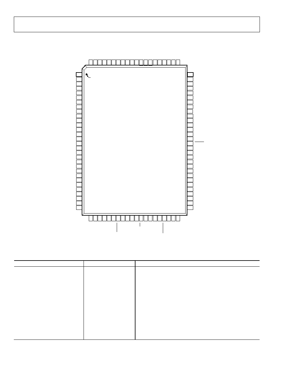
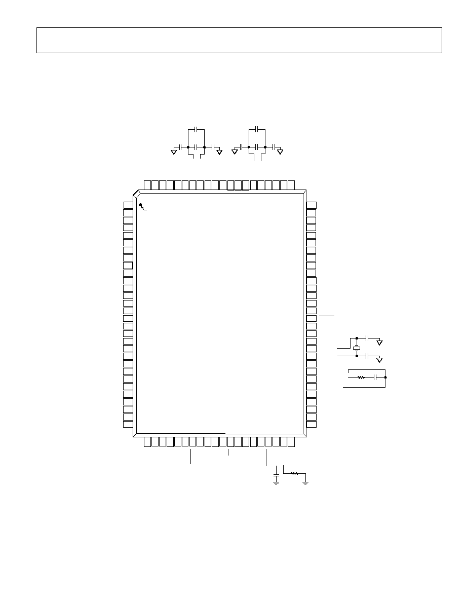
PIN CONFIGURATION AND FUNCTION DESCRIPTIONS
31
TxIQ(1)
32
TxIQ(0)
33
DV
DD
34
DGND
35
PR
OFILE(
1)
36
PR
OFILE(
0)
37
R
ESET
38
DV
DD
39
DGND
40
DGND
41
SC
LK
42
CS
43
SD
IO
44
SD
O
2
DRGND
3
DRVDD
4
IF(11)
7
IF(8)
6
IF(9)
5
IF(10)
1
AVDD
8
IF(7)
9
IF(6)
10
IF(5)
12
IF(3)
13
IF(2)
14
IF(1)
15
IF(0)
16
RxIQ(3)
17
RxIQ(2)
18
RxIQ(1)
19
RxIQ(0)
20
RxSYNC
21
DRGND
22
DRVDD
23
MCLK
24
DVDD
25
DGND
26
TxSYNC
27
TxIQ(5)
28
TxIQ(4)
29
TxIQ(3)
30
TxIQ(2)
11
IF(4)
79
I IN+
78
I IN≠
77
AGNDIQ
74
AGNDIQ
75
NC
76
NC
80
AGNDIQ
73
AVDDIQ
72
DRVDD
71
REFCLK
69
DGNDSD
68
SDELTA0
67
SDELTA1
66
DVDDSD
65
CA_EN
64
CA_DATA
63
CA_CLK
62
DVDDOSC
61
OSCIN
60
XTAL
59
DGNDOSC
58
AGNDPLL
57
PLLFILT
56
AVDDPLL
55
DVDDPLL
54
DGNDPLL
53
AVDDTx
52
Tx+
51
Tx≠
70
DRGND
45
DGNDTx
46
DV
DDTx
47
P
W
RDN
48
RE
FIO
49
FS
ADJ
50
AGNDTx
NC
AGND
IF12+
IF12
≠
AGND
AV
DD
REFT12
RE
FB1
2
AV
DD
AGND
NC
NC
AGND
AV
DD
REFT8
RE
FB8
AV
DD
AGND
Q IN+
Q IN≠
100
99
98
97
96
95
94
93
92
91
90
89
88
87
86
85
84
83
82
81
PIN 1
AD9877
TOP VIEW
(Not to Scale)
NC = NO CONNECT
02716-002
Figure 2. Pin Configuration
Table 3. Pin Function Descriptions
Pin No.
Mnemonic
Description
1, 84, 87, 92, 95
AVDD
12-Bit ADC Analog 3.3 V Supply.
2, 21, 70
DRGND
Pin Driver Digital Ground.
3, 22, 72
DRVDD
Pin Driver Digital 3.3 V Supply.
25, 34, 39, 40
DGND
Digital Ground.
24, 33, 38
DVDD
Digital 3.3 V Supply.
45
DGNDTx
Tx Path Digital Ground.
46
DVDDTx
Tx Path Digital 3.3 V Supply.
50
AGNDTx
Tx Path Analog Ground.
53
AVDDTx
Tx Path Analog 3.3 V Supply.
54
DGNDPLL
PLL Digital Ground.
55
DVDDPLL
PLL Digital 3.3 V Supply.
56
AVDDPLL
PLL Analog 3.3 V Supply.
58
AGNDPLL
PLL Analog Ground.

AD9877
Rev. B | Page 9 of 36
Pin No.
Mnemonic
Description
59
DGNDOSC
Oscillator Digital Ground.
62
DVDDOSC
Oscillator Digital 3.3 V Supply.
66
DVDDSD
- Digital 3.3 V Supply.
69
DGNDSD
- Digital Ground.
73
AVDDIQ
8-Bit ADC Analog 3.3 V Supply.
74, 77, 80
AGNDIQ
8-Bit ADC Analog Ground.
83, 88, 91, 96, 99
AGND
12-Bit ADC Analog Ground.
4:15
IF[11:0]
12-Bit ADC Digital Output.
16:19
RxIQ[3:0]
Muxed I and Q ADC Output.
20
RxSYNC
Sync Output, IF, I, and Q ADCs.
23
MCLK
Master Clock Output.
26
TxSYNC
Sync Input for Transmit Port.
27:32 TxIQ[5:0]
Digital
Input for Transmit Port.
35, 36
PROFILE[1:0]
Profile Selection Inputs.
37
RESET
Chip Reset Input.
41 SCLK
SPORT
Clock.
42
CS
SPORT Chip Select.
43
SDIO
SPORT Data I/O.
44
SDO
SPORT Data Output.
47
PWRDN
Power-Down Transmit Path.
48
REFIO
TxDAC Decoupling (to AGND).
49
FSADJ
DAC Output Adjust (External Resistor).
51, 52
Tx-, Tx+
Tx Path Complementary Outputs.
57
PLLFILT
PLL Loop Filter Connection.
60
XTAL
Crystal Oscillator Inverse Output.
61 OSCIN
Oscillator
Clock
Input.
63
CA_CLK
Serial Clock to Cable Driver.
64
CA_DATA
Serial Data to Cable Driver.
65
CA_EN
Serial Enable to Cable Driver.
67
SDELTA1
- Output Stream1.
68
SDELTA0
- Output Stream0.
71 REFCLK
Programmable
Reference Clock Output.
75, 76, 89, 90, 100
NC
No Connect (Leave Floating).
78, 79
I IN-, I IN+
Differential Input to I ADC.
81, 82
Q IN-, Q IN+
Differential Input to Q ADC.
85
REFB8
8-Bit ADC Decoupling Node.
86
REFT8
8-Bit ADC Decoupling Node.
93
REFB12
12-Bit ADC Decoupling Node.
94
REFT12
12-Bit ADC Decoupling Node.
97, 98
IF12-, IF12+
Differential Input to IF ADC.
AD9877
Rev. B | Page 10 of 36
TYPICAL PERFORMANCE CHARACTERISTICS
V
AS
= 3.3 V, V
DS
= 3.3 V, f
OSCIN
= 27 MHz, f
SYSCLK
= 216 MHz, f
MCLK
= 54 MHz (M = 8 and N = 4). ADC sample rate derived directly from
f
OSCIN
, R
SET
= 4.02 k (I
OUT
= 10 mA), and 75 DAC load, unless otherwise noted.
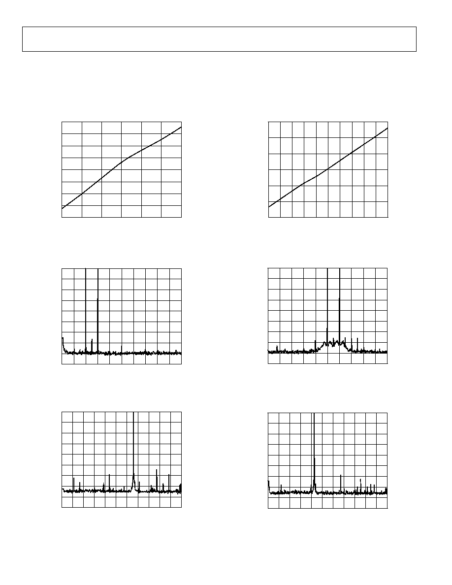
TYPICAL POWER CONSUMPTION CHARACTERISTICS
Transmitted 20 MHz single tone, unless otherwise noted.
f
SYSCLK
(MHz)
120
240
140
160
180
200
220
340
POWER
320
300
280
260
240
220
200
180
02716-
003
Figure 3. Power Consumption vs. Clock Speed, f
SYSCLK
02716-
004
% DUTY CYCLE
0
100
10
30
50
60
70
310
POWER
300
290
280
270
260
250
20
40
90
80
Figure 4. Power Consumption vs. Transmit Burst Duty Cycle
DUAL SIDEBAND TRANSMIT SPECTRUM
See Table 11 for dual-tone generation.
FREQUENCY (MHz)
0
2
2
6
10
12
14
0
MAGNITUDE (dB)
≠
20
≠
30
≠
50
≠
60
≠
70
≠
90
4
8
18
16
≠
80
≠
40
≠
10
0
02716-
005
Figure 5. Dual Sideband Spectral Plot, f
C
= 5 MHz, f = 1 MHz,
R
SET
= 4.02 K, DAC Gain = 7.5 dB, RBW = 1 kHz
FREQUENCY (MHz)
55
75
61
65
67
69
MAGNITUDE (dB)
59
63
73
71
0
≠
20
≠
30
≠
50
≠
60
≠
70
≠
90
≠
80
≠
40
≠
10
57
02716-
006
Figure 6. Dual Sideband Spectral Plot, f
C
= 65 MHz, f = 1 MHz,
R
SET
= 4.02 K, (I
OUT
= 10 mA), RBW = 1 kHz
SINGLE SIDEBAND TRANSMIT SPECTRUM
FREQUENCY (MHz)
0
110
30
50
60
70
0
MAGNITUDE (dB)
≠20
≠30
≠50
≠60
≠70
≠90
20
40
90
80
≠80
≠40
≠10
10
100
02716-
007
Figure 7. Single Sideband @ 65 MHz, RBW = 2 kHz, f
C
= 66 MHz,
f = 1 MHz, R
SET
= 4.02 K, DAC gain = 7.5 dB
FREQUENCY (MHz)
0
110
30
50
60
70
0
MAGNITUDE (dB)
≠20
≠30
≠50
≠60
≠70
≠90
20
40
90
80
≠80
≠40
≠10
10
100
02716-
008
Figure 8. Single Sideband @ 42 MHz, RBW = 2 kHz, f
C
= 43 MHz,
f = 1 MHz, R
SET
= 4.02 K, DAC gain = 7.5 dB
AD9877
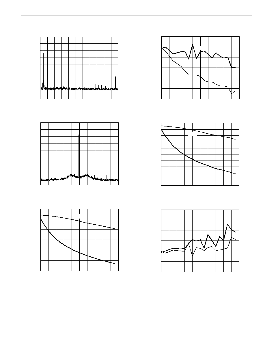
Rev. B | Page 11 of 36
FREQUENCY (MHz)
0
110
30
50
60
70
0
MAGNITUDE
(dB)
≠20
≠30
≠50
≠60
≠70
≠90
20
40
90
80
≠80
≠40
≠10
10
100
02716-009
Figure 9. Single Sideband @ 5 MHz, RBW = 2 kHz, f
C
= 6 MHz,
f = 1 MHz, R
SET
= 4.02 K, DAC gain = 7.5 dB
FREQUENCY (MHz)
62.5
67.5
64.0
65.0
65.5
0
MAGNITUDE
(dB)
≠20
≠30
≠50
≠60
≠70
≠90
63.5
64.5
66.5
66.0
≠80
≠40
≠10
63.0
67.0
02716-010
Figure 10. Single Sideband @ 65 MHz, RBW = 500 Hz, f
C
= 66 MHz,
f = 1 MHz, R
SET
= 4.02 K, DAC gain = 7.5 dB
f
IN
(MHz)
5
9
55
70
(dB)
60
50
45
40
15
45
75
55
65
25
35
65
85
105
5
PLL
f
OSCIN
02716-011
Figure 11. 12-Bit ADC SNR vs. Input Frequency
f
IN
(MHz)
5
9
55
90
(dB)
80
70
65
60
15
45
75
75
85
25
35
65
85
105
5
02716-012
f
OSCIN
PLL
Figure 12. 12-Bit ADC SFDR vs. Input Frequency
f
IN
(MHz)
5
9
55
11.0
EN
OB
9.0
7.5
7.0
6.0
15
45
75
8.5
10.0
25
35
65
85
105
PLL
10.5
9.5
6.5
8.0
5
02716-013
f
OSCIN
Figure 13. 12-Bit ADC ENOBs vs. Input Frequency
f
IN
(MHz)
5
9
55
≠
60
(dB)
≠
70
≠
80
≠
85
≠
90
15
45
75
≠
75
≠
65
25
35
65
85
105
5
f
OSCIN
PLL
02716-014
Figure 14. 12-Bit ADC THD vs. Input Frequency

AD9877
Rev. B | Page 12 of 36
TERMINOLOGY
Aperture Delay
The aperture delay is a measure of the sample-and-hold
amplifier (SHA) performance. It specifies the time delay
between the rising edge of the sampling clock input and when
the input signal is held for conversion.
Aperture Uncertainty (Jitter)
Aperture jitter is the variation in aperture delay for successive
samples. It is manifested as noise on the input to the ADC.
Channel-to-Channel Isolation (Crosstalk)
In an ideal multichannel system, the signal in one channel does
not influence the signal level of another channel. The channel-
to-channel isolation specification is a measure of the change
that occurs to a grounded channel as a full-scale signal is
applied to another channel.
Differential Nonlinearity Error (DNL, No Missing Codes)
An ideal converter exhibits code transitions that are exactly 1 LSB
apart. DNL is the deviation from this ideal value. Guaranteed
no missing codes to 10-bit resolution indicates that all 1,024
codes, respectively, must be present over all operating ranges.
Effective Number of Bits (ENOB)
For a sine wave, SINAD can be expressed in terms of the
number of bits. Using the formula
N = (SINAD - 1.76 dB/6.02)
it is possible to determine a measure of performance expressed
as N, the effective number of bits. Thus, the effective number of
bits for a device's sine wave inputs at a given input frequency
can be calculated directly from its measured SINAD.
Gain Error
The first code transition should occur at an analog value
1/2 LSB above full scale. The last transition should occur for an
analog value 1 1/2 LSB below the nominal full scale. Gain error
is the deviation of the actual difference between the first and
last code transitions and the ideal difference between the first
and last code transitions.
Input Referred Noise
The rms output noise is measured using histogram techniques.
The standard deviation of the ADC output code is calculated in
LSB and converted to an equivalent voltage. This results in a
noise figure that can be directly referred to the input of the MxFE.
Integral Nonlinearity Error (INL)
Linearity error refers to the deviation of each individual code
from a line drawn from negative full scale through the positive
full scale. The point used as the negative full scale occurs
1/2 LSB before the first code transition. Positive full scale is
defined as a level 1 1/2 LSB beyond the last code transition. The
deviation is measured from the middle of each code to the true
straight line.
Offset Error
First transition should occur for an analog value 1/2 LSB
above -FS. Offset error is defined as the deviation of the actual
transition from that point.
Output Compliance Range
The range of allowable voltage at the output of a current-output
DAC. Operation beyond the maximum compliance limits can
cause either output stage saturation or break down, resulting in
nonlinear performance.
Phase Noise
Single-sideband phase noise power is specified relative to the
carrier (dBc/Hz) at a given frequency offset (1 kHz) from the
carrier. Phase noise can be measured directly in single-tone
transmit mode with a spectrum analyzer that supports noise
marker measurements. It detects the relative power between the
carrier and the offset (1 kHz) sideband noise and takes the
resolution bandwidth (RBW) into account by subtracting
10 log(RBW). It also adds a correction factor that compensates
for the implementation of the resolution bandwidth, log display,
and detector characteristic.
Pipeline Delay (Latency)
Pipeline delay is the number of clock cycles between conversion
initiation and the availability of the associated output data.
Power Supply Rejection
Power supply rejection specifies the converter's maximum full-
scale change when the supplies are varied from nominal to
minimum and maximum specified voltages.
Signal-to-Noise and Distortion (SINAD) Ratio
SINAD is the ratio of the rms value of the measured input
signal to the rms sum of all other spectral components below
the Nyquist frequency, including harmonics but excluding dc.
The value for SINAD is expressed in decibels.
Signal-to-Noise Ratio (SNR)
SNR is the ratio of the rms value of the measured input signal to
the rms sum of all other spectral components below the Nyquist
frequency, excluding harmonics and dc. The value for SNR is
expressed in decibels.
Spurious-Free Dynamic Range (SFDR)
SFDR is the difference, in dB, between the rms amplitude of the
DAC output signal (or the ADC input signal) and the peak
spurious signal over the specified bandwidth (Nyquist
bandwidth, unless otherwise noted).
Total Harmonic Distortion (THD)
THD is the ratio of the rms sum of the first six harmonic
components to the rms value of the measured input signal and
is expressed as a percentage or in decibels.
AD9877
Rev. B | Page 13 of 36
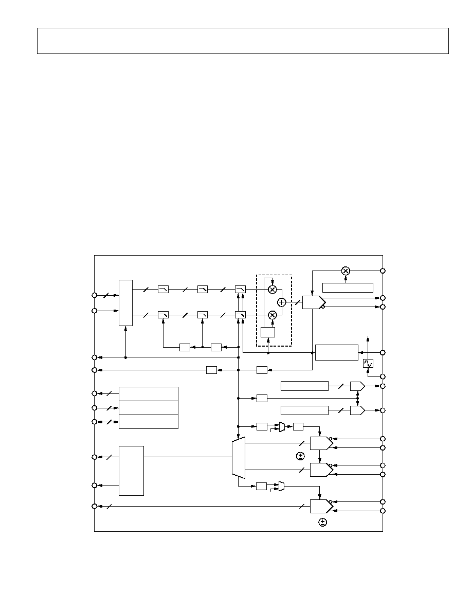
THEORY OF OPERATION
To gain a general understanding of the AD9877, refer to the
block diagram of the device architecture in Figure 15. The
following is a general description of the device functionality.
Later sections will detail each of the data path building blocks.
TRANSMIT SECTION
Modulation Mode Operation
The AD9877 accepts 6-bit words that are strobed synchronous
to the master clock, MCLK, into the data assembler. A high
level on TxSYNC signals the start of a transmit symbol. Two
successive 6-bit words form a 12-bit symbol component. The
incoming data is assumed to be complex in that alternating
12-bit words are regarded as the in-phase (I) and quadrature
(Q) components of a symbol. Symbol components are assumed
to be in twos complement format. The rate at which the TxIQ
data is read will be referred to as the master clock rate (f
MCLK
).
The data assembler receives the multiplexed IQ data and creates
two parallel 12-bit paths with I and Q data pairs, which
compose a complex symbol. The rate at which the I and Q data-
word pairs appear at the output of the data assembler are
referred to as the IQ sample rate (f
IQCLK
). Because four 6-bit
reads are required at the TxIQ input to read a full 24-bit
complex symbol, f
MCLK
is 4 times the IQ sample rate (f
MCLK
= 4 ◊
f
IQCLK
).
Once through the data assembler, the IQ data streams are fed
through two half-band filters (Half-Band Filters 1 and 2). The
combination of these two filters results in the sample rate
increasing by a factor of 4. Thus, at the output of Half-Band
Filter 2, the sample rate is 4 ◊ f
IQCLK
. In addition to the sample
rate increase, the half-band filters provide the low-pass filtering
characteristic necessary to suppress the spectral images
produced by the upsampling process.
IF12 INPUT
Q INPUT
I INPUT
SDELTA1
XTAL
Tx
FSADJ
SDELTA0
OSCIN
12
8
8
ADC
ADC
ADC
CONTROL WORD 0
CONTROL WORD 1
-
-
12
12
M = 1, 2, ..., 31
OSCIN
MULTIPLIER
◊
M
˜
8
˜
2
˜
2
˜
N
REF12
REF8
˜
2
MUX
DAC
DAC GAIN CONTROL
N = 3, 4
(f
OSCIN
)
(f
OSCIN
)
(f
SYSCLK
)
(f
OSCIN
)
12
QUADRATURE
MODULATOR
DDS
SIN
HALF-BAND
FILTER 1
HALF-BAND
FILTER 2
CIC
FILTER
DATA
ASSEMBLER
I
Q
COS
AD832x CTRL
BURST PROFILE CTRL
SERIAL INTERFACE
3
2
4
RxIQ
DATA
4
12
12
12
12
12
12
12
˜
2
˜
2
R = 2, 3, ..., 63
˜
R
(f
IQCLK
)
(f
MCLK
)
AD9877
6
TxIQ
Rx IF
RxSYNC
RxIQ
REFCLK
MCLK
TxSYNC
02716-015
Figure 15. Block Diagram

AD9877
Rev. B | Page 14 of 36
After passing through the half-band filter stages, the IQ data
streams are fed to a cascaded integrator-comb (CIC) filter. This
filter is configured as an interpolating filter, which allows
further upsampling rates of 3 or 4. The CIC filter, like the half-
bands, has a built-in low-pass characteristic. Again, this
provides for suppression of the spectral images produced by the
upsampling process.
The digital quadrature modulator stage following the CIC filters
is used to frequency shift (upconvert) the baseband spectrum of
the incoming data stream up to the desired carrier frequency.
The carrier frequency is controlled numerically by a direct
digital synthesizer (DDS). The DDS uses the internal system
clock (f
SYSCLK
) to generate the desired carrier frequency with a
high degree of precision. The carrier is applied to the I and Q
multipliers in quadrature fashion (90∞ phase offset) and
summed to yield a data stream that is the modulated carrier.
It should be noted at this point that the incoming data has been
converted from an input sample rate of f
MCLK
to an output
sample rate of f
SYSCLK
(see Figure 15). The modulated carrier
becomes the 12-bit samples sent to the DAC.
Single-Tone Output Transmit Operation
The AD9877 can be configured for frequency synthesis
applications by writing the single-tone bit true. In single-tone
mode, the AD9877 disengages the modulator and preceding
data path logic to output a spectrally pure single-frequency sine
wave. The AD9877 provides for a 26-bit frequency tuning word,
which results in a tuning resolution of 3.2 Hz at a f
SYSCLK
rate of
216 MHz. A good rule when using the AD9877 as a frequency
synthesizer is to limit the fundamental output frequency to 30%
of f
SYSCLK
. This avoids generating aliases too close to the desired
fundamental output frequency, thus minimizing the cost of
filtering the aliases.
Frequency hopping via the profile inputs and associated tuning
word is also supported in single-tone mode, which allows
frequency shift keying (FSK) modulation.
OSCIN Clock Multiplier
As mentioned earlier, the output data is sampled at the rate of
f
SYSCLK
. The AD9877 has a built-in programmable clock
multiplier and an oscillator circuit. This allows the use of a
relatively low frequency, and therefore less expensive, crystal or
oscillator to generate the OSCIN signal. The low frequency
OSCIN signal can then be multiplied in frequency by an integer
factor of between 1 and 31, inclusive, to become the f
SYSCLK
clock.
For DDS applications, the carrier is typically limited to about
30% of f
SYSCLK
. For a 65 MHz carrier, the system clock required is
above 216 MHz.
The OSCIN multiplier function maintains clock integrity, as
evidenced by the excellent phase noise characteristics and low
clock-related spur in the output spectrum of the AD9877.
External loop filter components consisting of a series resistor
(1.3 k) and capacitor (0.01 F) provide the compensation zero
for the OSCIN multiplier PLL loop. The overall loop
performance has been optimized for these component values.
Receive Section
The AD9877 includes three high speed, high performance
ADCs. Two matched 8-bit ADCs are optimized for analog IQ
demodulated signals and can be sampled at rates up to
16.5 MSPS. A direct IF 12-bit ADC can sample signals at rates
up to 33 MSPS.
The ADC sampling frequency can be derived directly from the
OSCIN signal or from the on-chip OSCIN multiplier. For
highest dynamic performance, it is recommended to choose an
OSCIN frequency that can be directly used as the ADC
sampling clock. Digital 8-bit ADC outputs are multiplexed to
one 4-bit bus, clocked by the master clock (MCLK). The 12-bit
ADC uses a nonmultiplexed 12-bit interface with an output
data rate of half the f
MCLK
frequency.
CLOCK AND OSCILLATOR CIRCUITRY
The internal oscillator of the AD9877 generates all sampling
clocks from a simple, low cost, parallel resonance, fundamental
frequency quartz crystal. Figure 16 shows how the quartz
crystal is connected between OSCIN (Pin 61) and XTAL
(Pin 60) with parallel resonant load capacitors as specified by
the crystal manufacturer. The internal oscillator circuitry can
also be overdriven by a clock applied to OSCIN with XTAL left
unconnected.
f
OSCIN
= f
MCLK
◊ N/M
An internal phase-locked loop (PLL) generates the DAC
sampling frequency, f
SYSCLK
, by multiplying OSCIN frequency M
times. The MCLK signal (Pin 23), f
MCLK
, is derived by dividing
this PLL output frequency by N (Register Address 0x01).
f
SYSCLK
= f
OSCIN
◊ M
f
MCLK
= f
OSCIN
◊ M/N
An external PLL loop filter (Pin 57) consisting of a series
resistor and ceramic capacitor (Figure 16, R1 = 1.3 k, C12 =
0.01 F) is required for stability of the PLL. Also, a shield
surrounding these components is recommended to minimize
external noise coupling into the PLL's voltage-controlled
oscillator input (guard trace connected to AVDDPLL).
Figure 15 shows that ADCs are either sampled directly by a low
jitter clock at OSCIN or by a clock that is derived from the PLL
output. Operating modes can be selected in Register 0x08.
Sampling the ADCs directly with the OSCIN clock requires
MCLK to be programmed at twice the OSCIN frequency.
AD9877
Rev. B | Page 15 of 36
PROGRAMMABLE CLOCK OUTPUT REFCLK
The AD9877 provides a frequency-programmable clock output
REFCLK (Pin 71). OSCIN or MCLK (f
MCLK
) and the master
clock divider ratio R stored in Register Address 0x01 determine
its frequency.
f
OSCOUT
= f
MCLK
/R or f
OSCIN
In its default setting (0x00 in Register 0x01), the REFCLK pin
provides a buffered output of f
OSCIN
.
31
TxIQ(1)
32
TxIQ(0)
33
DV
DD
34
DGND
35
PR
OFILE(
1)
36
PR
OFILE(
0)
37
R
ESET
38
DV
DD
39
DGND
40
DGND
41
SC
LK
42
CS
43
SD
IO
44
SD
O
2
DRGND
3
DRVDD
4
(MSB) IF(11)
7
IF(8)
6
IF(9)
5
IF(10)
1
AVDD
8
IF(7)
9
IF(6)
10
IF(5)
12
IF(3)
13
IF(2)
14
IF(1)
15
IF(0)
16
(MSB) RxIQ(3)
17
RxIQ(2)
18
RxIQ(1)
19
RxIQ(0)
20
RxSYNC
21
DRGND
22
DRVDD
23
MCLK
24
DVDD
25
DGND
26
TxSYNC
27
(MSB) TxIQ(5)
28
TxIQ(4)
29
TxIQ(3)
30
TxIQ(2)
11
IF(4)
79
I IN+
78
I IN≠
77
AGNDIQ
74
AGNDIQ
75
NC
76
NC
80
AGNDIQ
73
AVDDIQ
72
DRVDD
71
REFCLK
69
DGNDSD
68
SDELTA0
67
SDELTA1
66
DVDDSD
65
CA_EN
64
CA_DATA
63
CA_CLK
62
DVDDOSC
61
OSCIN
60
XTAL
59
DGNDOSC
58
AGNDPLL
57
PLLFILT
56
AVDDPLL
55
DVDDPLL
54
DGNDPLL
53
AVDDTx
52
Tx+
51
Tx≠
70
DRGND
45
DGNDTx
46
DV
DDTx
47
P
W
RDN
48
RE
FIO
49
FS
ADJ
50
AGNDTx
NC
AGND
IF12+
IF12
≠
AGND
AV
DD
REFT12
RE
FB1
2
AV
DD
AGND
NC
NC
AGND
AV
DD
REFT8
RE
FB8
AV
DD
AGND
Q IN+
Q IN
≠
100
99
98
97
96
95
94
93
92
91
90
89
88
87
86
85
84
83
82
81
PIN 1
AD9877
TOP VIEW
(Pins Down)
NC = NO CONNECT
02716-016
C3
0.1
F
C6
0.1
F
C1
0.1
F
C4
0.1
F
CP1
10
F
CP2
10
F
C2
0.1
F
C5
0.1
F
C10
20pF
C11
20pF
GUARD TRACE
C12
0.01
F
R1
1.3k
C13
0.1
F
R
SET
2k
Figure 16. Basic Connection Diagram
AD9877
Rev. B | Page 16 of 36
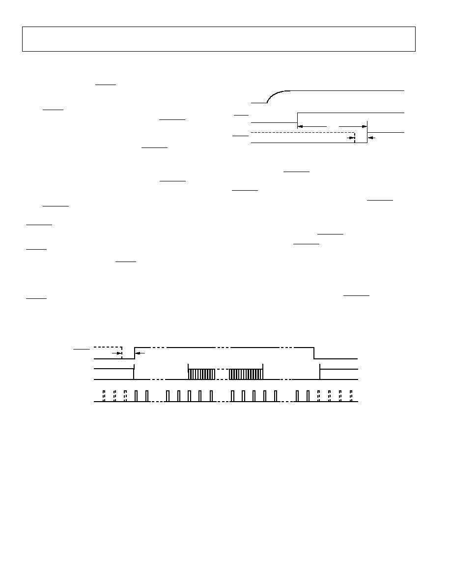
RESET AND TRANSMIT POWER-DOWN
Power-Up Sequence
On initial power-up, the RESET pin should be held low until
the power supply is stable.
Once RESET is deasserted, the AD9877 can be programmed
over the serial port. It is recommended that the PWRDN pin be
held low during the reset. Changes to ADC Clock Select
(Register 0x08) or SYS Clock Divider N (Register 0x01) should
be programmed before the rising edge of PWRDN. Changes to
the multiplier (M) will require the PLL to reacquire the new
frequency, which can take up to 1 ms.
Once the PLL is frequency-locked and after the PWRDN pin is
brought high, transmit data can be sent reliably.
If the PWRDN pin cannot be held low throughout the reset and
PLL settling time period, the Power-Down Digital Tx bit or the
PWRDN pin should be pulsed after the PLL has settled. This
will ensure correct transmit filter initialization.
RESET
To initiate a hardware reset, the RESET pin should be held low
for at least 100 ns. All internally generated clocks except
REFCLK stop during reset. The MCLK signal begins
transmission three clock cycles after reset. The rising edge of
RESET reinitializes the programmable registers to their default
values. The same sequence as described in the Power-Up
Sequence section should be followed after a reset or change in M.
A software reset (writing a 1 into Bit 5 of Register 0x00) is
functionally equivalent to the hardware reset but does not force
Register 0x00 to its default value.
02716-
017
V
S
1ms
5 MCLK
RESET
PWRDN
Figure 17. Power-Up Sequence for Tx Data Path
Transmit Power-Down
A low level on the PWRDN pin stops all clocks linked to the
digital transmit data path and resets the CIC filter. Deasserting
PWRDN reactivates all clocks. The CIC filter is held in a reset
state for 80 MCLK cycles after the rising edge of PWRDN to
allow for flushing of the half-band filters with new input data.
Transmit data bursts should be padded with at least 20 symbols
of null data directly before the PWRDN pin is asserted.
Immediately after the PWRDN pin is deasserted, the transmit
burst should start with a minimum of 20 null data symbols.
This avoids unintended DAC output samples caused by the
transmit path latency and filter settling time.
Software Power-Down Digital Tx (Bit 5 in Register 0x02) is
functionally equivalent to the hardware PWRDN pin and takes
effect immediately after the last register bit has been written
over the serial port.
PWRDN
TxIQ
TxSYNC
5 MCLK
20 NULL SYMBOLS
DATA SYMBOLS
20 NULL SYMBOLS
0
0
0
0
0
0
0
0
02716-018
Figure 18. Timing Sequence to Flush Tx Data Path
AD9877
Rev. B | Page 17 of 36
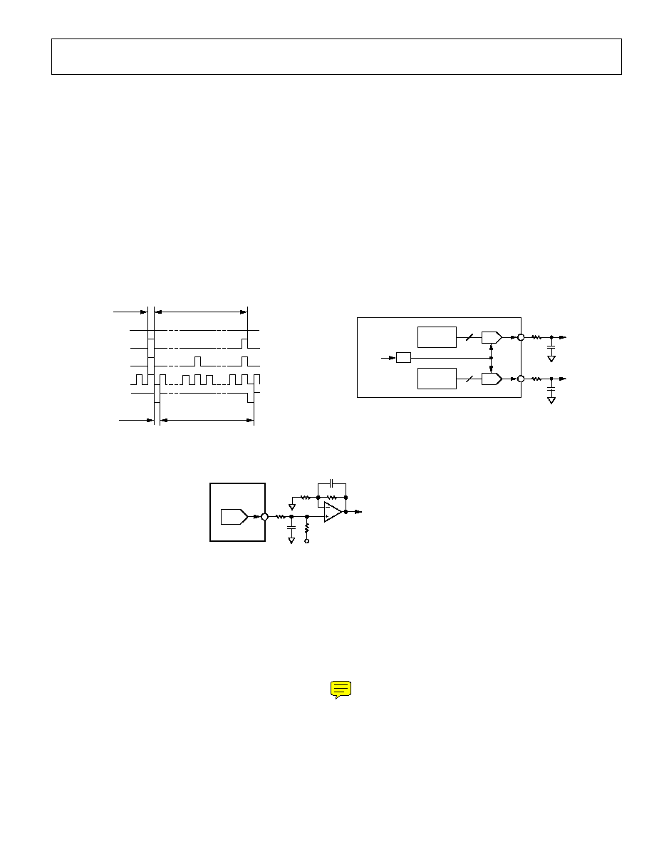
- OUTPUTS
The AD9877 contains two independent - outputs that
provide a digital logic bit stream with an average duty cycle that
varies between 0% and (4095/4096)%, depending on the
programmed code, as shown in Figure 19.
These bit streams can be low-pass filtered to generate
programmable dc voltages of
V
DC
= (- Code/4096)(V
H
) + V
L
where:
V
H
= V
DRVDD
- 0.6 V.
V
L
= 0.4 V.
In set-top box and cable modem applications, the outputs can
be used to control external variable gain amplifiers and RF
tuners. A simple single-pole RC low-pass filter provides
sufficient filtering (Figure 20).
In more demanding applications where additional gain, level
shift, or drive capability is required, a first or second order
active filter might be considered for each - output (Figure 21).
0x000
0x001
0x002
0x800
0xFFF
4096
◊
8
t
MCLK
4096
◊
8
t
MCLK
8
t
MCLK
8
t
MCLK
02716-019
Figure 19. - Output Signals
-
-
CONTROL
WORD 0
CONTROL
WORD 1
12
12
SIGMA-DELTA 0
SIGMA-DELTA 1
R
R
C
C
DC (0.4 TO
DRVDD ≠ 0.6V)
DC (0.4 TO
DRVDD ≠ 0.6V)
TYPICAL:
R = 50k
C = 0.01
F
f
≠3dB
= 1/(2
RC) = 318Hz
˜
8
MCLK
AD9877
02716-
020
Figure 20. - RC Filter
R
C
V
OUT
= (V
SD
+ V
OFFSET
) (1 + R/R1)/2
TYPICAL:
R = 50k
C = 0.01
F
f
≠3dB
= 1/(2
RC) = 318Hz
AD9877
R
V
OFFSET
OP250
R1
R
C
V
SD
V
OUT
-
02716-021
Figure 21. - Active Filter with Gain and Offset

AD9877
Rev. B | Page 18 of 36
REGISTER MAP AND BIT DEFINITIONS
Table 4. Register Map
1
Address
(Hex)
Bit 7
Bit 6
Bit 5
Bit 4
Bit 3
Bit 2
Bit 1
Bit 0
Default
(Hex) Type
0x00 SDIO
Bidirectional
LSB First
RESET
OSCIN Multiplier M [4]
08 Read/write
0x01 PLL
Lock
Detect
SYSCLK
Divider
N = 3
(N = 4
Default)
MCLK Divider R [5:0]
00 Read/write
0x02 Power-
Down PLL
Power-
Down
DAC Tx
Power-Down
Digital Tx
Power-
Down
12-Bit
ADC
Power-Down
12-Bit ADC
Reference
0 0
Power-
Down
8-Bit
ADC
00 Read/write
0x03
- Output [0] Control Word [3:0] LSB
0
0
0
Flag [0]
Enable
00 Read/write
-
0x04
Flag [0]
- Output 0 Control Word [11:4] MSB
00
Read/write -
0x05
- Output [0] Control Word [3:0] LSB
0
0
0
Flag [1]
Enable
00 Read/write
-
0x06
Flag [1]
- Output 1 Control Word [11:4] MSB
00
Read/write -
0x07 0
0
0
0
0
0 0
0
00 Read/write
Tx
0x08 ADC
Clock
Select
0 0
Power-
Down
RxSYNC
and 8-
Bit ADC
Clock
0 0
0
0
80
Read/write
ADC
0x09 0
0
0
0
0
0 0
0
00 Read/write
0x0A 0
0
0
0
0
0 0
0
00 Read
only
0x0B 0
0
0
0
0
0 0
0
00 Read/write
0x0C 0
0
0
1
Version
[3:0]
10 Read
only
0x0D
Tx Frequency Tuning
Word Profile 3 LSBs [1:0]
Tx Frequency Tuning
Word Profile 2 LSBs [1:0]
Tx Frequency Tuning
Word Profile 1 LSB [1:0]
Tx Frequency Tuning
Word Profile 3 LSBs [1:0]
00 Read/write
Tx
0x0E
0
0
0
0
DAC Gain Control [3:0]
00 Read/write
Tx
0x0F
0
0
Profile Select [1:0]
CA Interface
Mode Select
0 Spectral
Inversion Tx
Single-
Tone Tx
Mode
00 Read/write
Tx
0x10
Tx Frequency Turning Word Profile 0 [9:2]
00 Read/write
Tx
0x11
Tx Frequency Turning Word Profile 0 [17:10]
00 Read/write
Tx
0x12
Tx Frequency Turning Word Profile 0 [25:18]
00 Read/write
Tx
0x13
CA Interface Transmit Word Control Profile 0 [7:4]
DAC Gain Control Profile 0 [3:0]
00 Read/write
Tx
0x14
Tx Frequency Turning Word Profile 1 [9:2]
00 Read/write
Tx
0x15
Tx Frequency Turning Word Profile 1 [9:2]
00 Read/write
Tx
0x16
Tx Frequency Turning Word Profile 1 [9:2]
00 Read/write
Tx
0x17
CA Interface Transmit Word Control Profile 1 [7:4]
DAC Gain Control Profile 1 [3:0]
00 Read/write
Tx
0x18
Tx Frequency Turning Word Profile 2 [9:2]
00 Read/write
Tx
0x19
Tx Frequency Turning Word Profile 2 [9:2]
00 Read/write
Tx
1A
Tx Frequency Turning Word Profile 2 [9:2]
00 Read/write
Tx
0x1B
CA Interface Transmit Word Control Profile 2 [7:4]
DAC Gain Control Profile 2 [3:0]
00 Read/write
Tx
0x1C
Tx Frequency Turning Word Profile 3 [9:2]
00 Read/write
Tx
0x1D
Tx Frequency Turning Word Profile 3 [9:2]
00 Read/write
Tx
0x1E
Tx Frequency Turning Word Profile 3 [9:2]
00 Read/write
Tx
0x1F
CA Interface Transmit Word Control Profile 3 [7:4]
DAC Gain Control Profile 3 [3:0]
00 Read/write
Tx
1
Register bits denoted with 0 must be programmed with a 0 each time that register is written.

AD9877
Rev. B | Page 19 of 36
REGISTER 0x00--INITIALIZATION
Bits 0≠4: OSCIN Multiplier
This register field is used to program the on-chip multiplier
(PLL) that generates the chip's high frequency system clock f
SYSCLK
.
To multiply the external crystal clock f
OSCIN
by 16 decimals, for
example, program Register 0x00, Bits 4:0 as 0x10. The default
value of M is 0x08. Valid entries range from M = 1 to 31. When
M equals 1, the PLL is disabled. All internal clocks are derived
directly from OSCIN.
The PLL requires 200 MCLK cycles to regain frequency lock
after a change in M, the clock multiplier value. After the
recapture time of the PLL, the frequency of f
SYSCLK
is stable.
For timing integrity, certain restrictions on the values of M and
N apply when both AD9877 transmit and receive paths are
used. The supported modes are shown in Table 5.
Table 5. ADC Clock Select
ADC Clock Select
N
M
1, f
OSCIN
3 6
4 8
0, f
MCLK
(PLL derived)
3
12
4 16
Bit 5: RESET
Writing a 1 to this bit resets the registers to their default values
and restarts the chip. The RESET bit always reads back 0. The
bits in Register 0x00 are not affected by this software reset. A
low level at the RESET pin, however, would force all registers,
including all bits in Register 0x00, to their default state.
Bit 6: LSB First
Active high indicates SPI serial port access of instruction byte
and data registers are least significant bit (LSB) first. Default low
indicates most significant bit (MSB) first format.
Bit 7: SDIO Bidirectional
Active high configures the serial port as a three-signal port with
the SDIO pin used as a bidirectional input/output pin. Default
low indicates the serial port uses four signals with SDIO con-
figured as an input and SDO configured as an output.
REGISTER 0x01--CLOCK CONFIGURATION
Bits 0≠5: MCLK Divider
This register determines the output clock on the REFCLK pin.
At default zero (R = 0), REFCLK provides a buffered version of
the OSCIN clock signal for other chips.
The register can also be used to divide the chip's master clock,
f
MCLK
, by R, where R is an integer between 2 and 63. The
generated reference clock on the REFCLK pin can be used for
external frequency controlled devices.
Bit 6: SYSCLK Divider
The OSCIN multiplier output clock, f
SYSCLK
, can be divided by 4
or 3 to generate the chip's master clock. Active high indicates a
divide ratio of N = 3. Default low configures a divide ratio of
N = 4.
Bit 7: PLL Lock Detect
When this bit is set low, the REFCLK pin functions in its default
mode and provides an output clock with frequency f
MCLK
/R, as
described previously.
If this bit is set to 1, the REFCLK pin is configured to indicate
whether the PLL is locked to f
OSCIN
. In this mode, the REFCLK
pin should be low-pass filtered with an RC filter of 1.0 k and
0.1 F. A high output on REFCLK indicates the PLL has
achieved lock with f
OSCIN
.
REGISTER 0x02--POWER-DOWN
Sections of the chip that are not used can be powered down
when the corresponding bits are set high. This register has a
default value of 0x00, with all sections active.
Bit 0: Power-Down 8-Bit ADC
Active high powers down the 8-bit ADC.
Bit 3: Power-Down 12-Bit ADC Reference
Active high powers down the 12-bit ADC reference.
Bit 4: Power-Down 12-Bit ADC
Active high powers down the 12-bit ADC.
Bit 5: Power-Down Digital Tx
Active high powers down the digital transmit section of the
chip, similar to the function of the PWRDN pin.
Bit 6: Power-Down DAC Tx
Active high powers down the DAC.
Bit 7: Power-Down PLL
Active high powers down the OSCIN multiplier.
REGISTER 0x03≠0x06--- CONTROL WORDS
The - control words are 12 bits wide and split into MSB Bits
[11:4] and LSB Bits [3:0]. Changes to the - control words
take effect immediately for every MSB or LSB register write.
- output control words have a default value of 0. The control
words are in straight binary format, with 0x000 corresponding
to the bottom of the scale and 0xFFF corresponding to the top
of the scale (see Figure 19 for details).
If flag enable (Bit 0 of Register 0x03 or 0x05) is set high, the
SDELTA pins maintains a fixed logic level determined directly
by the MSB of the - control word.

AD9877
Rev. B | Page 20 of 36
REGISTER 0x08--ADC CLOCK CONFIGURATION
Bit 4: Power-Down RxSYNC and 8-Bit ADC Clock
Setting this bit to 1 powers down the sampling clock of the 8-bit
ADC and stops the RxSYNC output pin. It can be used for
additional power saving on top of the power-down selections in
Register 0x02.
Bit 7: ADC Clock Select
When set high, the input clock at OSCIN is used directly as the
ADC sampling clock. When set low, the internally generated
master clock, MCLK, is used as the ADC sampling clock. Best
ADC performance is achieved when the ADCs are sampled
directly from f
OSCIN
using an external crystal or low jitter crystal
oscillator.
REGISTER 0x0C--DIE REVISION
Bits 0≠3: Version
The die version of the chip can be read from this register.
REGISTER 0x0D--Tx FREQUENCY TUNING WORDS
LSBs
This register accommodates 2 LSBs for each of the four
frequency tuning words (see the Registers 0X10≠0X1F--Burst
Parameter section).
REGISTER 0x0E--DAC GAIN CONTROL
This register allows the user to program the DAC gain if Tx
Gain Control Select Bit 3 in Register 0x0F is set to 0.
Table 6. DAC Gain Control
Bits [3:0]
DAC Gain
0000
0.0 dB (default)
0001 0.5
dB
0010 1.0
dB
0011 1.5
dB
... ...
1110 7.0
dB
1111 7.5
dB
REGISTER 0x0F--Tx PATH CONFIGURATION
Bit 0: Single-Tone Tx Mode
Active high configures the AD9877 for single-tone applications
such as FSK. The AD9877 will supply a single-frequency output
as determined by the frequency tuning word selected by the
active profile. In this mode, the TxIQ input data pins are
ignored but should be tied to a valid logic voltage level. Default
value is 0 (inactive).
Bit 1: Spectral Inversion Tx
When set to 1, inverted modulation is performed.
MODULATOR_OUT = [I cos(t) + Q sin(t)]
Default is logic low, noninverted modulation.
MODULATOR_OUT = [I cos(t) - Q sin(t)]
Bit 3: CA Interface Mode Select
This bit changes the manner in which transmit gain control is
performed. Typically, either AD8321/AD8325 (Default 0) or
AD8322/AD8327 (Default 1) variable gain cable amplifiers are
programmed over the chip's 3-wire cable amplifier (CA)
interface. The Tx gain control select changes the interpretation
of the bits in Registers 0x13, 0x17, 0x1B, and 0x1F (see the
Cable Driver Gain Control section).
Bits 4≠5: Profile Select
The AD9877 quadrature digital upconverter is capable of
storing four preconfigured modulation modes called profiles.
Each profile defines a transmit frequency tuning word and cable
driver amplifier gain (DAC gain) setting. Profile Select [1:0] bits
or PROFILE [1:0] pins program the current register profile to
be used. Profile Select bits should always be 0 if PROFILE[1:0]
pins are used to switch between profiles. Using the Profile Select
bits as a means of switching between different profiles requires
the PROFILE [1:0] pins to be tied low.
REGISTERS 0x10≠0x1F--BURST PARAMETER
Tx Frequency Tuning Words
The frequency tuning word (FTW) determines the DDS-
generated carrier frequency (f
C
) and is formed via a
concatenation of register addresses.
The 26-bit FTW is spread over four register addresses. Bit 25 is
the MSB, and Bit 0 is the LSB.
The carrier frequency equation is given as
fc = [FTW ◊ f
SYSCLK
]/2
26
where:
f
SYSCLK
= M ◊ f
OSCIN
.
FTW < 0 ◊ 2000000.
Changes to FTW bytes take effect immediately.
Cable Driver Gain Control
The AD9877 has a three-pin interface to the AD832x family of
programmable gain cable driver amplifiers. This allows direct
control of the cable driver's gain through the AD9877.
In its default mode, the complete 8-bit register value is
transmitted over the 3-wire CA interface.
If Bit 3 of Register 0x0F is set high, Bits [7:4] determine the
8-bit word sent over the CA interface according to Table 7.

AD9877
Rev. B | Page 21 of 36
Table 7. Cable Driver Gain Control
Bits [7:4]
CA Interface Transmit Word
0000
0000 0000 (default)
0001 0000
0001
0010 0000
0010
0011 0000
0100
0100 0000
1000
0101 0001
0000
0110 0010
0000
0111 0100
0000
1000 1000
0000
In this mode, the lower bits determine the fine gain setting of
the DAC output.
Table 8. DAC Output Fine Gain Setting
Bits [3:0]
DAC Fine Gain
0000
0.0 dB (default)
0001 0.5
dB
0010 1.0
dB
0011 1.5
dB
... ...
1110 7.0
dB
1111 7.5
dB
New data is automatically sent over the 3-wire CA interface
(and DAC gain adjust) whenever the value of the active gain
control register changes or a new profile is selected. The default
value is 0x00 (lowest gain).
The formula for the combined output level calculation of the
AD9877 fine gain and the AD8327 or AD8322 coarse gain is
V
8327
= V
9877(0)
+ (fine)/2 + 6(coarse) - 19
V
8322
= V
9877(0)
+ (fine)/2 + 6(coarse) - 14
where:
fine is the decimal value of Bits [3:0].
coarse is the decimal value of Bits [7:8].
V
9877(0)
is the level at AD9877 output in dBmV for fine = 0.
V
8327
is the level at output of the AD8327 in dBmV.
V
8322
is the level at output of the AD8322 in dBmV.

AD9877
Rev. B | Page 22 of 36
SERIAL INTERFACE FOR REGISTER CONTROL
The AD9877 serial port is a flexible, synchronous serial
communication port allowing easy interface to many industry-
standard microcontrollers and microprocessors. The interface
allows read/write access to all registers that configure the
AD9877. Single or multiple byte transfers are supported. Also,
the interface can be programmed to read words either MSB first
or LSB first. The serial interface port I/O of the AD9877 can be
configured to have one bidirectional I/O (SDIO) pin or two
unidirectional I/O (SDIO/SDO) pins.
GENERAL OPERATION OF THE SERIAL INTERFACE
There are two phases to a communication cycle with the
AD9877. Phase 1 is the instruction cycle, which is the writing of
an instruction byte into the AD9877 that is coincident with the
first eight SCLK rising edges. The instruction byte provides the
AD9877 serial port controller with information regarding the
data transfer cycle, Phase 2 of the communication cycle. The
Phase 1 instruction byte defines whether the upcoming data
transfer is a read or write, the number of bytes in the data
transfer, and the starting register address for the first byte of the
data transfer. The first eight SCLK rising edges of each
communication cycle are used to write the instruction byte into
the AD9877.
The eight remaining SCLK edges are for Phase 2 of the
communication cycle. Phase 2 is the actual data transfer
between the AD9877 and the system controller. Phase 2 of the
communication cycle is a transfer of 1 to 4 data bytes as
determined by the instruction byte. Registers change
immediately upon writing to the last bit of each transfer byte.
INSTRUCTION BYTE
Table 9 illustrates the information contained in the instruction byte.
Table 9. Instruction Byte Information
MSB
LSB
I7
I6 I5 I4 I3 I2 I1 I0
R/W
N1 N0 A4 A3 A2 A1 A0
The R/W bit of the instruction byte determines whether a read
or a write data transfer will occur after the instruction byte
write. Logic high indicates a read operation. Logic low indicates
a write operation. The N1:N0 bits determine the number of
bytes to be transferred during the data transfer cycle. The bit
decodes are shown in Table 10.
Table 10. Bit Decodes
N1 N0 Description
0 0 Transfer
1
byte
0 1 Transfer
2
bytes
1 0 Transfer
3
bytes
1 1 Transfer
4
bytes
The Bits A4:A0 determine which register is accessed during the
data transfer portion of the communication cycle. For multibyte
transfers, this address is the starting byte address. The
remaining register addresses are generated by the AD9877.
SERIAL INTERFACE PORT PIN DESCRIPTION
SCLK--Serial Clock
The serial clock pin is used to synchronize data transfers from
the AD9877 and to run the serial port state machine. The
maximum SCLK frequency is 15 MHz. Input data to the
AD9877 is sampled upon the rising edge of SCLK. Output data
changes upon the falling edge of SCLK.
CS--Chip Select
Active low input starts and gates a communication cycle. It
allows multiple devices to share a common serial port bus. The
SDO and SDIO pins go to a high impedance state when CS is
high. Chip select should stay low during the entire
communication cycle.
SDIO--Serial Data I/O
Data is always written into the AD9877 on this pin. However,
this pin can be used as a bidirectional data line. The configuration
of this pin is controlled by Bit 7 of Register 0x00. The default is
Logic 0, which configures the SDIO pin as unidirectional.
SDO--Serial Data Out
Data is read from this pin for protocols that use separate lines
for transmitting and receiving data. When the AD9877 operates
in a single bidirectional I/O mode, this pin does not output data
and is set to a high impedance state.
MSB/LSB TRANSFERS
The AD9877 serial port can support both the MSB-first or the
least significant bit LSB-first data formats. This functionality is
controlled by the LSB-first bit in Register 0x00. The default is
MSB first.
When this bit is set active high, the AD9877 serial port is in
LSB-first format. In LSB-first mode, the instruction byte and
data bytes must be written from the LSB to the MSB. In LSB-
first mode, the serial port internal byte address generator
increments for each byte of the multibyte communication cycle.
AD9877
Rev. B | Page 23 of 36
When this bit is set default low, the AD9877 serial port is in
MSB-first format. In MSB-first mode, the instruction byte and
data bytes must be written from the MSB to the LSB. In MSB-
first mode, the serial port internal byte address generator
decrements for each byte of the multibyte communication cycle.
When incrementing from 0x1F, the address generator changes
to 0x00. When decrementing from 0x00, the address generator
changes to 0x1F.
NOTES ON SERIAL PORT OPERATION
The AD9877 serial port configuration bits reside in Bit 6 and
Bit 7 of Register 0x00. It is important to note that the
configuration changes immediately upon writing to the last bit
of the register. For multibyte transfers, writing to this register
may occur during the middle of the communication cycle.
Care must be taken to compensate for this new configuration
for the remaining bytes of the current communication cycle.
The same considerations apply to setting the RESET bit in
Register 0x00. All other registers are set to their default values,
but the software reset does not affect the bits in Register 0x00. It
is recommended to use only single-byte transfers when chang-
ing serial port configurations or initiating a software reset.
A write to Bits 1, 2, and 3 of Register 0x00 with the same logic
levels as Bits 7, 6, and 5 (bit pattern: XY1001YX binary) allows
the host processor to reprogram a lost serial port configuration
and to reset the registers to their default values. A second write
to Register 0x00 with RESET bit low and serial port configura-
tion as specified above (XY) reprograms the OSCIN multiplier
setting. A changed f
SYSCLK
frequency is stable after a maximum
of 200 f
MCLK
cycles.
CS
R/W N1
N0
A4
A3
A2
A1
A0 D7n D6n
D20 D10 D00
D7n D6n
D20 D10 D00
SCLK
INSTRUCTION CYCLE
DATA TRANSFER CYCLE
SDIO
SDO
02716-022
Figure 22. Serial Register Interface Timing MSB First
D00 D10 D20
D6n D7n
SCLK
INSTRUCTION CYCLE
DATA TRANSFER CYCLE
SDIO
SDO
CS
A0
A1
A2
A3
A4
N0
N1 R/W D00 D10 D20
D6n D7n
02716-023
Figure 23. Serial Register Interface Timing LSB First
02716-024
SCLK
INSTRUCTION BIT 7
INSTRUCTION BIT 6
t
SCLK
t
DH
t
PWL
t
PWH
t
DS
SDIO
CS
t
DS
Figure 24. Timing Diagram for Register Write to AD9877
02716-025
SCLK
SDIO
SDO
CS
DATA BIT N
DATA BIT N ≠ 1
t
DV
Figure 25. Timing Diagram for Register Read from AD9877

AD9877
Rev. B | Page 24 of 36
TRANSMIT PATH (Tx)
t
SU
t
HD
MCLK
TxSYNC
TxIQ
TxI[11:6]
TxI[5:0]
TxQ[11:6]
TxQ[5:0]
TxI[11:6]
TxI[5:0]
TxQ[11:6]
TxQ[5:0]
TxI[11:6]
TxI[5:0]
02716-026
Figure 26. Transmit Timing Diagram
TRANSMIT TIMING
The AD9877 provides a master clock, MCLK, and expects 6-bit
multiplexed TxIQ data upon each rising edge. Transmit
symbols are framed with the TxSYNC input. TxSYNC high
indicates the start of a transmit symbol. Four consecutive 6-bit
data packages form a symbol (I MSB, I LSB, Q MSB, and Q LSB).
DATA ASSEMBLER
The input data stream is representative complex data. Two 6-bit
words form a 12-bit symbol component (twos complement
format). Four input samples are required to produce one I/Q
data pair. The I/Q sample rate, f
IQCLK
, at the input to the first
half-band filter is a quarter of the input data rate, f
MCLK
.
The I/Q sample rate, f
IQCLK
, puts a bandwidth limit on the
maximum transmit spectrum. This is the familiar Nyquist limit
and is equal to one-half f
IQCLK
, hereafter referred to as f
NYQ
.
HALF-BAND FILTERS (HBFs)
HBF 1 and HBF 2 are both interpolating filters, each of which
doubles the sampling rate. Together, HBF 1 and HBF 2 have
26 taps and provide a factor of 4 increase in the sampling rate
(4 ◊ f
IQCLK
or 8 ◊ f
NYQ
).
In relation to phase response, both HBFs are linear phase filters.
As such, virtually no phase distortion is introduced within the
pass band of the filters. This is an important feature, because
phase distortion is generally intolerable in a data transmission
system.
CASCADED INTEGRATOR-COMB (CIC) FILTER
A CIC filter is unlike a typical FIR filter in that it offers the
flexibility to handle differing input and output sample rates in
any integer ratios. In the AD9877, the CIC filter is configured as
a programmable interpolator and provides a sample rate
increase by a factor of R = 3 or R = 4. In addition to the ability
to provide a change in the sample rate between the input and
output, a CIC filter has an intrinsic low-pass frequency response
characteristic.
The frequency response of a CIC filter is dependent on three
factors:
∑
The rate change ratio, R.
∑
The order of the filter, n.
∑
The number of unit delays per stage, m.
It can be shown that the system function H(z) of a CIC filter is
given by
n
Rm
k
k
Rm
z
R
z
z
R
Hz
=
-
-
=
-
=
-
-
-
1
0
1
1
1
1
1
The form on the far right has the advantage of providing a
result for z = 1 (corresponding to zero frequency or dc). The
alternate form yields an indeterminate form (0/0) for z = 1, but
is otherwise identical. The only variable parameter for the CIC
filter of the AD9877 is R; m and n are fixed at 1 and 3,
respectively. Thus, the CIC system function for the AD9877
simplifies to
3
1
0
3
1
1
1
1
1
=
-
-
=
-
=
-
-
-
Rm
k
k
R
z
R
z
z
R
Hz
The transfer function is given by
( )
(
)
( )
( )
3
3
)
2
(
/
2
sin
sin
1
1
1
1
=
-
-
=
-
-
f
fR
R
e
e
R
f
H
f
j
R
j
The frequency response in this form is such that f is scaled to
the output sample rate of the CIC filter. That is, f = 1
corresponds to the frequency of the output sample rate of the
CIC filter. H(z) yields the frequency response with respect to
the input sample of the CIC filter.
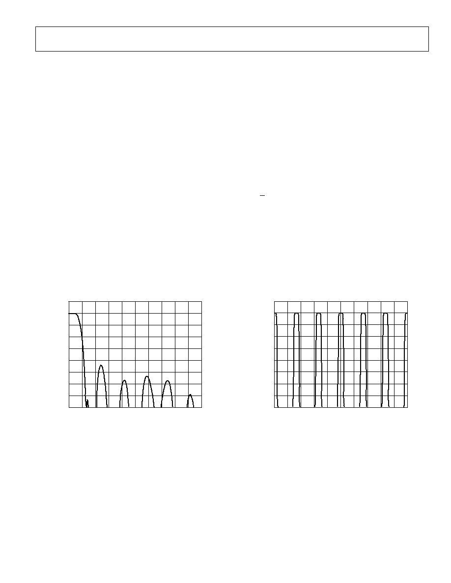
AD9877
Rev. B | Page 25 of 36
COMBINED FILTER RESPONSE
The combined frequency response of HBF 1, HBF 2, and CIC is
shown in Figure 27, Figure 28, Figure 29, Figure 31, Figure 32,
and Figure 33.
The usable bandwidth of the filter chain puts a limit on the
maximum data rate that can be propagated through the
AD9877. A look at the pass-band detail of the combined filter
response (Figure 30 and Figure 34) indicates that to maintain an
amplitude error of no more than 1 dB, use signals having a
bandwidth of no more than about 60% of f
NYQ
.
To keep the bandwidth of the data in the flat portion of the filter
pass band, the user must oversample the baseband data by at
least a factor of 2 prior to representing it to the AD9877. With-
out oversampling, the Nyquist bandwidth of the baseband data
corresponds to the f
NYQ
. Consequently, the upper end of the data
bandwidth suffers 6 dB or more of attenuation due to the
frequency response of the digital filters.
There is an additional concern if the baseband data applied to
the AD9877 has been pulse shaped. Typically, pulse shaping is
applied to the baseband data via a filter having a raised cosine
response.
In such cases, an value is used to modify the bandwidth of the
data where the value of is such that 0 1. A value of 0
causes the data bandwidth to correspond to the Nyquist
bandwidth. A value of 1 causes the data bandwidth to be
extended to twice the Nyquist bandwidth.
Thus, with 2◊ oversampling of the baseband data and = 1, the
Nyquist bandwidth of the data corresponds with the I/Q
Nyquist bandwidth. As stated earlier, this results in problems
near the upper edge of the data bandwidth due to the frequency
response of the filters. The maximum value of that can be
implemented is 0.45. This is because the data bandwidth
becomes
(
)
NYQ
NYQ
f
f
725
.
0
1
2
1
=
+
which puts the data bandwidth at the extreme edge of the flat
portion of the filter response.
If a particular application requires an value between 0.45
and 1, the user must oversample the baseband data by at least a
factor of 4. The combined HBF1, HBF2, and CIC filter
introduces a worst-case droop of less than 0.2 dB over the
frequency range of the data to be transmitted.
FREQUENCY (f
S
/2)
0
1.0
0.1
0.2
0.3
0.4
0.5
0.6
0.7
0.8
0.9
10
0
MAGNITUDE
(dB)
≠
10
≠
20
≠
30
≠
40
≠
50
≠
60
≠
70
≠
80
02716-027
Figure 27. Cascaded Filter 12◊ Interpolator (N = 3)
FREQUENCY (f
S
/2)
0
1.0
0.1
0.2
0.3
0.4
0.5
0.6
0.7
0.8
0.9
10
0
MAGNITUDE
(dB)
≠
10
≠
20
≠
30
≠
40
≠
50
≠
60
≠
70
≠
80
02716-028
Figure 28. Input Signal Spectrum (N = 3), = 0.25
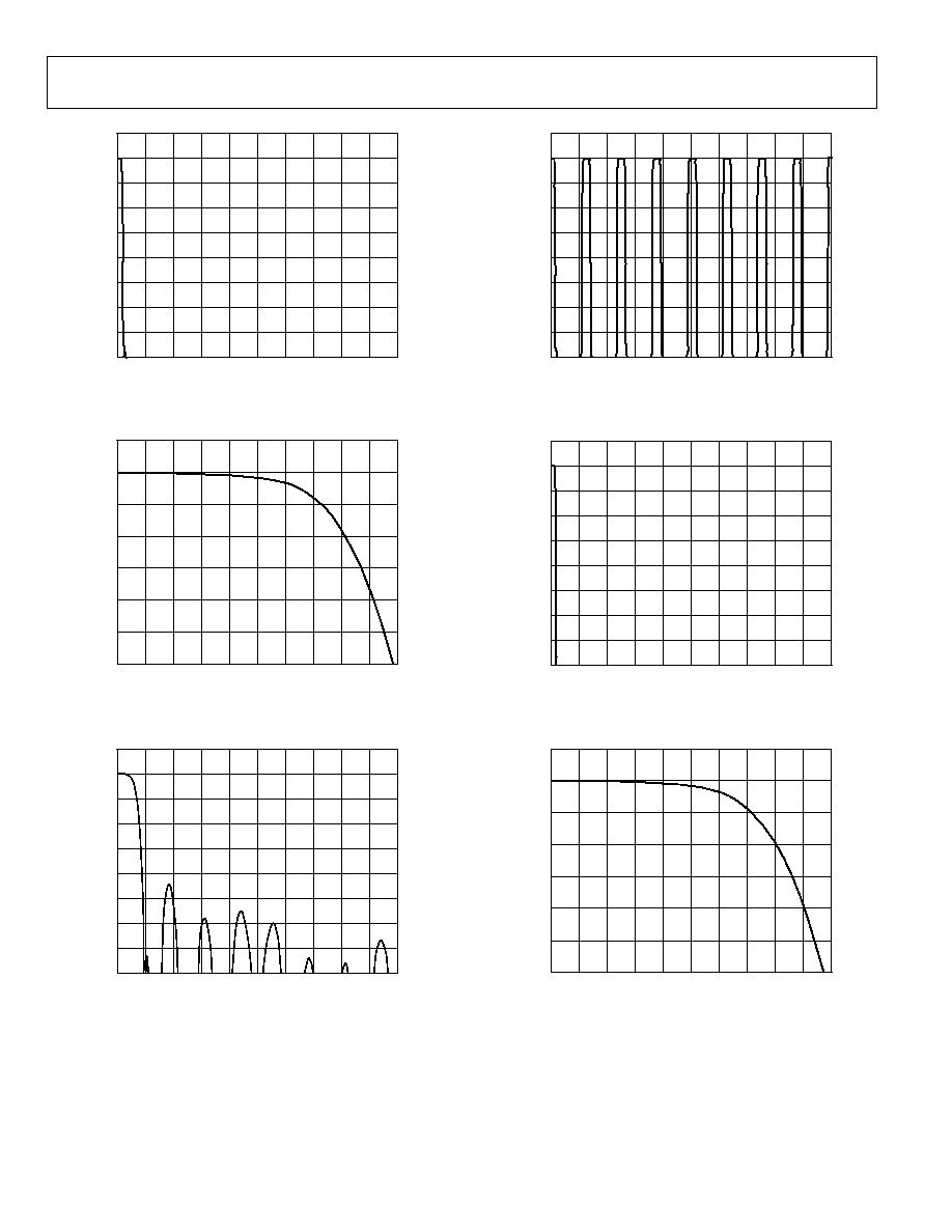
AD9877
Rev. B | Page 26 of 36
FREQUENCY (f
S
/2)
0
1.0
0.1
0.2
0.3
0.4
0.5
0.6
0.7
0.8
0.9
10
0
MAGNITUDE
(dB)
≠
10
≠
20
≠
30
≠
40
≠
50
≠
60
≠
70
≠
80
02716-029
Figure 29. Response to Input Signal Spectrum (N = 3)
02716-030
FREQUENCY RELATIVE TO I/Q NYQUIST BW
0
1.0
0.1
0.2
0.3
0.4
0.5
0.6
0.7
0.8
0.9
1
0
MAGNITUDE
(dB)
≠
1
≠
2
≠
3
≠
4
≠
5
≠
6
Figure 30. Cascaded Filter Pass-Band Detail (N = 3)
FREQUENCY (f
S
/2)
0
1.0
0.1
0.2
0.3
0.4
0.5
0.6
0.7
0.8
0.9
10
0
MAGNITUDE
(dB)
≠
10
≠
20
≠
30
≠
40
≠
50
≠
60
≠
70
≠
80
02716-031
Figure 31. Cascaded Filter 16◊ Interpolator (N = 4)
FREQUENCY (f
S
/2)
0
1.0
0.1
0.2
0.3
0.4
0.5
0.6
0.7
0.8
0.9
10
0
MAGNITUDE
(dB)
≠
10
≠
20
≠
30
≠
40
≠
50
≠
60
≠
70
≠
80
02716-032
Figure 32. Input Signal Spectrum (N = 4), = 0.25
FREQUENCY (f
S
/2)
0
1.0
0.1
0.2
0.3
0.4
0.5
0.6
0.7
0.8
0.9
10
0
MAGNITUDE
(dB)
≠
10
≠
20
≠
30
≠
40
≠
50
≠
60
≠
70
≠
80
02716-033
Figure 33. Response to Input Signal Spectrum (N = 4)
02716-034
FREQUENCY RELATIVE TO I/Q NYQUIST BW
0
1.0
0.1
0.2
0.3
0.4
0.5
0.6
0.7
0.8
0.9
1
0
MAGNITUDE
(dB)
≠1
≠2
≠3
≠4
≠5
≠6
Figure 34. Cascaded Filter Pass-Band Detail (N = 4)

AD9877
Rev. B | Page 27 of 36
Q
X
Z
X
I
02716-035
Figure 35. 16-Quadrature Modulation
Tx SIGNAL LEVEL CONSIDERATIONS
The quadrature modulator introduces a maximum gain of 3 dB
in the signal level. To visualize this, assume that both the I data
and Q data are fixed at the maximum possible digital value, x.
Then the output of the modulator, z, is
z = [x cos(t) - x sin(t)]
It can be shown that |z| assumes a maximum value of
(
)
(
)
dB
3
2
2
2
+
=
+
=
of
gain
a
x
x
x
z
However, if the same number of bits are used to represent the |z|
values as is used to represent the x values, an overflow occurs.
To prevent this possibility, an effective -3 dB attenuation is
internally implemented on the I and Q data path.
(
)
(
)
x
z
=
+
=
2
/
1
2
/
1
The following example assumes a Pk/rms level of 10 dB:
Maximum Symbol Component Input Value =
±(2,047 LSBs - 0.2 dB) = ±2,000 LSBs
Maximum Complex Input RMS Value =
2,000 LSBs + 6 dB - Pk/rms (dB) = 1,265 LSBs rms
Maximum complex input rms value calculation uses both I and
Q symbol components, which adds a factor of 2 (6 dB) to the
formula.
Table 11 shows typical IQ input test signals with amplitude
levels related to 12-bit full scale (FS).
ATTENUATOR
≠3dB
MODULATOR
3dB MAX
I
O
O
I
ATTENUATOR
≠3dB
TWOS COMPLEMENT FORMAT
HBF + CIC
INTERPOLATOR
+0.2dB
HBF + CIC
INTERPOLATOR
+0.2dB
12
12
I
O
COMPLEX DATA INPUT
DAC
02716-036
Figure 36. Signal Level Contribution
Tx THROUGHPUT AND LATENCY
Data inputs impact the output fairly quickly but remain
effective due to the filter characteristics of the AD9877. Data
transmit latency through the AD9877 is easiest to describe in
terms of f
SYSCLK
clock cycles (4 f
MCLK
). The numbers quoted are
when an effect is first seen after an input value changes.
Latency of I/Q data entering the data assembler (AD9877 input)
to the DAC output is 119 f
SYSCLK
clock cycles (29.75 f
MCLK
cycles).
DC values applied to the data assembler input take up to 176
f
SYSCLK
clock cycles (44 f
MCLK
cycles) to propagate and settle at the
DAC output.
Frequency hopping is accomplished via changing the PROFILE
input pins. The time required to switch from one frequency to
another is less than 232 f
SYSCLK
cycles (58.5 f
MCLK
cycles).
DIGITAL-TO-ANALOG CONVERTER
A 12-bit digital-to-analog converter (DAC) is used to convert
the digitally processed waveform into an analog signal. The
worst-case spurious signals due to the DAC are the harmonics
of the fundamental signal and their aliases. The conversion
process produces aliased components of the fundamental signal
at n ◊ f
SYSCLK
± f
CARRIER
(n = 1, 2, and 3). These are typically
filtered with an external RLC filter at the DAC output.
It is important for this analog filter to have a sufficiently flat
gain and linear phase response across the bandwidth of interest
to avoid modulation impairments. A relatively inexpensive
seventh-order elliptical low-pass filter is sufficient to suppress
the aliased components for HFC network applications.
Table 11. IQ Input Test Signals
Analog Output
Digital Input
Input Level
Modulator Output Level
Single Tone (f
C
- f)
I = cos(f)
FS - 0.2 dB
FS - 3.0 dB
Q = cos(f + 90∞) = -sin(f)
FS - 0.2 dB
Single Tone (f
C
+ f)
I = cos(f)
FS - 0.2 dB
FS - 3.0 dB
Q = cos(f + 270∞) = +sin(f)
FS - 0.2 dB
Dual Tone (f
C
± f)
I = cos(f)
FS - 0.2 dB
FS
Q = cos(f + 180∞) = -cos(f) or Q = +cos(f)
FS - 0.2 dB
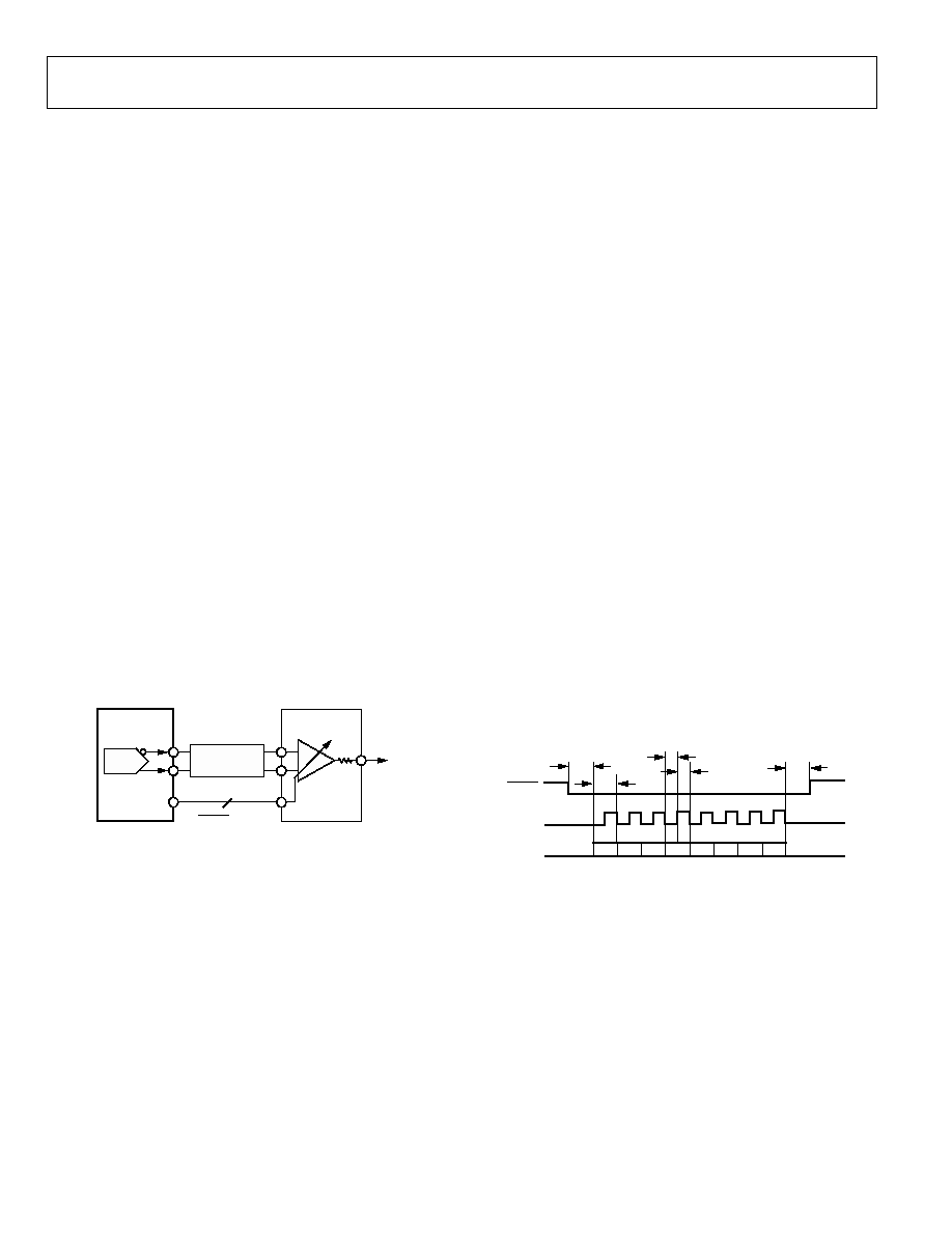
AD9877
Rev. B | Page 28 of 36
The AD9877 provides true and complement current outputs.
The full-scale output current is set by the R
SET
resistor at Pin 49
and the DAC gain register. Assuming maximum DAC gain, the
value of R
SET
for a particular full-scale I
OUT
is determined using
the following equation:
R
SET
= 32 V
DACRSET
/I
OUT
= 39.4/I
OUT
For example, if a full-scale output current of 20 mA is desired,
then R
SET
= (39.4/0.02) or approximately 2 k.
The following equation calculates the full-scale output current,
including the programmable DAC gain control.
I
OUT
= [39.4/R
SET
] ◊ 10
(-7.5 + 0.5 NGAIN)/20
where N
GAIN
is the value of DAC fine gain control [3:0].
The full-scale output current range of the AD9877 is 4 to
20 mA. Full-scale output currents outside of this range degrade
SFDR performance. SFDR is also slightly affected by output
matching; the two outputs should be terminated equally for best
SFDR performance. The output load should be located as close
as possible to the AD9877 package to minimize stray
capacitance and inductance. The load can be a simple resistor to
ground, an op amp current-to-voltage converter, or a
transformer-coupled circuit. It is best not to attempt to directly
drive highly reactive loads (such as an LC filter). Driving an LC
filter without a transformer requires that the filter be doubly
terminated for best performance.
The filter input and output should both be resistively
terminated with the appropriate values. The parallel
combination of the two terminations will determine the load
that the AD9877 will see for signals within the filter pass band.
For example, a 50 terminated input/output low-pass filter will
look like a 25 load to the AD9877. The output compliance
voltage of the AD9877 is -0.5 V to +1.5 V. To avoid signal
distortion, any signal developed at the DAC output should not
exceed 1.5 V. Furthermore, the signal may extend below ground
as much as 0.5 V without damage or signal distortion.
The AD9877 true and complement outputs can be differentially
combined for common-mode rejection using a broadband 1:1
transformer. Using a grounded center tap results in signals at
the AD9877 DAC output pins that are symmetrical about
ground. As previously mentioned, by differentially combining
the two signals, the user can provide some degree of common-
mode signal rejection. A differential combiner might consist of
a transformer or an operational amplifier. The object is to
combine or amplify only the difference between two signals and
to reject any common, usually undesirable characteristic, such
as 60 Hz hum or clock feedthrough that is equally present on
both individual signals.
Connecting the AD9877 true and complement outputs to the
differential inputs of the gain programmable cable drivers
AD8321/AD8323 or AD8322/AD8327 provides an optimized
solution for the standard compliant cable modem upstream
channel. The cable driver's gain can be programmed through a
direct 3-wire interface using the profile registers of the AD9877.
3
LOW-PASS
FILTER
Tx
AD832x
AD9877
CA
75
VARIABLE GAIN
CABLE DRIVER
AMPLIFIER
CA_EN
CA_DATA
CA_CLK
DAC
02716-037
Figure 37. Cable Amplifier Connection
CA_EN
CA_CLK
CA_DATA
MSB
8
t
MCLK
8
t
MCLK
8
t
MCLK
4
t
MCLK
4
t
MCLK
LSB
02716-038
Figure 38. Cable Amplifier Interface Timing

AD9877
Rev. B | Page 29 of 36
PROGRAMMING THE AD8321/AD8325 OR AD8322/AD8327 CABLE DRIVER AMPLIFIER
GAIN CONTROL
Programming the gain of the AD832x family cable driver
amplifier can be accomplished via the AD9877 cable amplifier
control interface. Four 8-bit registers within the AD9877 (one
per profile) store the gain value to be written to the serial 3-wire
port. Typically either AD8321/AD8325 or AD8322/AD8327
variable gain cable amplifiers are connected to the chip's 3-wire
cable amplifier interface. The Tx gain control select bit in
Register 0x0F changes the interpretation of the bits in Registers
0x13, 0x17, 0x1B, and 0x1F. See the Cable Driver Gain Control
section register description.
Data transfers to the gain programmable cable driver amplifier
are initiated by the following four conditions.
1. Power-Up and Hardware Reset--Upon initial power-up
and every hardware reset, the AD9877 clears the contents
of the gain control registers to 0, which defines the lowest
gain setting of the AD832x. Thus, the AD9877 writes all 0s
out of the 3-wire cable amplifier control interface.
2. Software Reset--Writing a 1 to Bit 5 of Address 0x00
initiates a software reset. Upon a software reset, the
AD9877 clears the contents of the gain control registers to
0 for the lowest gain and sets the profile select to 0. The
AD9877 writes all 0s out of the 3-wire cable amplifier
control interface if the gain was previously on a different
setting (other than 0).
3. Change in Profile Selection--The AD9877 samples the
PROFILE(1) and PROFILE(2) input pins together with the
two profile select bits and writes to the AD832x gain
control registers if a change in profile and gain is
determined. The data written to the cable driver amplifier
comes from the AD9877 gain control register associated
with the current profile.
4. Write to AD9877 Cable Driver Amplifier Control
Registers--The AD9877 will write gain control data
associated with the current profile to the AD832x
whenever the selected AD9877 cable driver amplifier gain
setting is changed.
Once a new stable gain value has been detected (48 MCLK to
64 MCLK cycles after initiation), a data write starts with CA_CS
going low. The AD9877 always finishes a write sequence to the
cable driver amplifier once it is started. The logic controlling
data transfers to the cable driver amplifier uses up to 200 MCLK
cycles and is designed to prevent erroneous write cycles from
occurring.
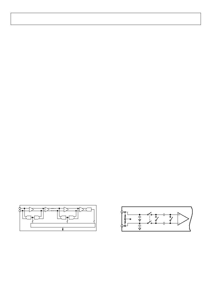
AD9877
Rev. B | Page 30 of 36
RECEIVE PATH (Rx)
ADC THEORY OF OPERATION
The analog-to-digital converters of the AD9877 implement
pipelined multistage architectures to achieve high sample rates
while consuming low power. Each ADC distributes the
conversion over several smaller ADC subblocks, refining the
conversion with progressively higher accuracy as it passes the
results from stage to stage.
As a consequence of the distributed conversion, ADCs require a
small fraction of the 2
n
comparators used in a traditional n-bit
flash-type ADC. A sample-and-hold function within each of the
stages permits the first stage to operate on a new input sample
while the remaining stages operate on preceding samples. Each
stage of the pipeline, excluding the last, consists of a low
resolution flash ADC connected to a switched capacitor DAC
and interstage residue amplifier (MDAC). The residue amplifier
amplifies the difference between the reconstructed DAC output
and the flash input for the next stage in the pipeline. One bit of
redundancy is used in each stage to facilitate digital correction
of flash errors. The last stage simply consists of a flash ADC.
The analog inputs of the AD9877 incorporate a novel structure
that merges the input sample-and-hold amplifiers (SHA) and
the first pipeline residue amplifiers into single, compact
switched capacitor circuits. This structure achieves considerable
noise and power savings over a conventional implementation
that uses separate amplifiers by eliminating one amplifier in the
pipeline. By matching the sampling network of the input SHA
with the first stage flash ADC, the ADCs can sample inputs well
beyond the Nyquist frequency with no degradation in
performance.
The digital data outputs of the ADCs are represented in straight
binary format. They saturate to full scale or zero scale when the
input signal exceeds the input voltage range.
RECEIVE TIMING
The AD9877 sends multiplexed data to the RxIQ outputs upon
every rising edge of MCLK. The data stream consists of two
nibbles of I data followed by two nibbles of Q data. The
RxSYNC pulse frames the I/Q data and is coincidentally high
with the most significant nibble of the I data-word. If the 8-bit
I/Q ADC is in power-down mode, the RxSYNC signal will not
be generated.
The 12-bit ADC data is sent to the IF[11:0] outputs upon every
second falling edge of MCLK.
In its default setting, the REFCLK pin provides a buffered
version of f
OSCIN
. REFCLK can be used as a qualifying clock for
the Rx data when the ratio between the OSCIN multiplier and
the OSCIN divider is programmed to be 2 (M/N = 2) or when
the ADC sampling is selected to be derived from f
OSCIN
directly.
DRIVING THE ANALOG INPUTS
Figure 40 illustrates the equivalent analog inputs of the AD9877
(a switched capacitor input). Bringing CLK to a logic high
opens Switch S3 and closes Switches S1 and S2. The input
source is connected to AIN and must charge capacitor C
H
during this time. Bringing CLK to a logic low opens switch S2,
and then Switch S1 opens followed by closing switch S3. This
places the input into hold mode.
The structure of the input SHA places certain requirements on
the input drive source. The combination of the pin capacitance
and the hold capacitance of C
H
is typically less than 5 pF. The
input source must be able to charge or discharge this
capacitance to its n-bit accuracy in one-half of a clock cycle.
When the SHA goes into track mode, the input source must
charge or discharge capacitor C
H
from the voltage already stored
on C
H
to the new voltage. In the worst case, a full-scale voltage
step on the input source must provide the charging current
through the R
ON
(100 ) of Switch S1 and quickly (within
1/2 CLK period) settle. This situation corresponds to driving a
low input impedance.
D/A
A/D
A/D
SHA
CORRECTION LOGIC
D/A
A/D
SHA
GAIN
AINP
AINN
AD9877
02716-
039
Figure 39. ADC Architecture
AINP
AINN
2k
2k
V
BIAS
S1
S3
C
P
C
P
C
H
C
H
S2
AD9877
02716-040
Figure 40. Differential Input Architecture
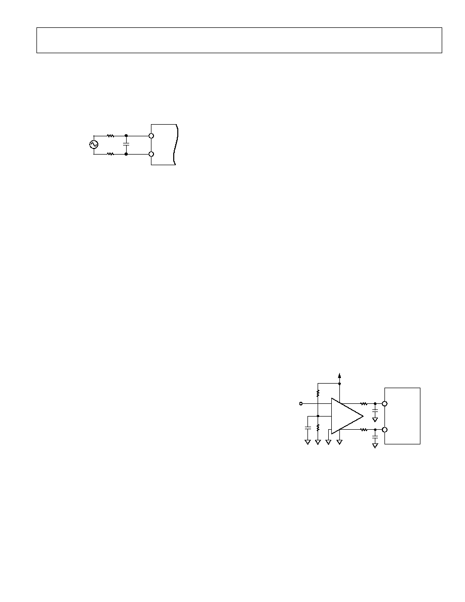
AD9877
Rev. B | Page 31 of 36
On the other hand, when the source voltage equals the value
previously stored on C
H
, the hold capacitor requires no input
current and the equivalent input impedance is extremely high.
Adding series resistance between the output of the signal source
and the AIN pin reduces the drive requirements placed on the
signal source. Figure 41 shows this configuration.
AINP
AINN
<50
SHUNT
<50
V
S
02716-041
Figure 41. Simple ADC Drive Configuration
The bandwidth of the particular application limits the size of
this resistor. To maintain the performance outlined in the data
sheet specifications, the resistor should be limited to 50 or
less. For applications with signal bandwidths less than 10 MHz,
the user can proportionally increase the size of the series
resistor. Alternatively, adding a shunt capacitance between the
AIN pins can lower the ac load impedance. The value of this
capacitance will depend on the source resistance and the
required signal bandwidth. In systems that must use dc-
coupling, use an op amp to comply with the input requirements
of the AD9877.
OP AMP SELECTION GUIDE
Op amp selection for the AD9877 is highly application
dependent. In general, the performance requirements of any
given application can be characterized by either time domain or
frequency domain constraints. In either case, one should
carefully select an op amp that preserves the performance of the
ADC. This task becomes challenging when one considers the
high performance capabilities of the AD9877 coupled with
other system level requirements, such as power consumption
and cost. The ability to select the optimal op amp can be further
complicated by either limited power supply availability and/or
limited acceptable supplies for a desired op amp.
Newer, high performance op amps typically have input and
output range limitations in accordance with their lower supply
voltages. As a result, some op amps will be more appropriate in
systems where ac coupling is allowed. When dc coupling is
required, op amp headroom constraints (such as rail-to-rail op
amps), or instances where larger supplies can be used, should be
considered.
Analog Devices offers differential output operational amplifiers,
such as the AD8131, with a fixed gain of 2. They can be used for
differential or single-ended-to-differential signal conditioning
with 8-bit performance to directly drive ADC inputs. The
AD8138 is a higher performance version of the AD8131. It
provides 12-bit performance and allows different gain settings.
Please contact the local sales office for updates on the latest
Analog Devices amplifier product offerings.
ADC DIFFERENTIAL INPUTS
The AD9877 uses a 1 V p-p input span for the 8-bit ADC inputs
and a 2 V p-p for the 12-bit ADC. Since not all applications
have a signal preconditioned for differential operation, there is
often a need to perform a single-ended-to-differential
conversion. In systems that do not need a dc input, an RF
transformer with a center tap is the best method to generate
differential inputs beyond 20 MHz for the AD9877. This
provides all the benefits of operating the ADC in the differential
mode without contributing additional noise or distortion. An
RF transformer also has the added benefit of providing
electrical isolation between the signal source and the ADC. An
improvement in THD and SFDR performance can be realized
by operating the AD9877 in differential mode. The
performance enhancement between the differential and single-
ended mode is most considerable as the input frequency
approaches and goes beyond the Nyquist frequency (f
IN
> f
S
/2).
The AD8131 provides a convenient method of converting a
single-ended signal to a differential signal. This is an ideal
method for generating a signal directly coupled to the AD9877.
The AD8131 will accept a signal swinging below 0 V and shift it
to an externally provided common-mode voltage. The AD8131
configuration is shown in Figure 42.
R2
R2
R1
R1
≠
+
AINP
AINN
AD9877
SINGLE-ENDED
ANALOG INPUT
02716-042
AD8131
Figure 42. Single-Ended-to-Differential Input Drive
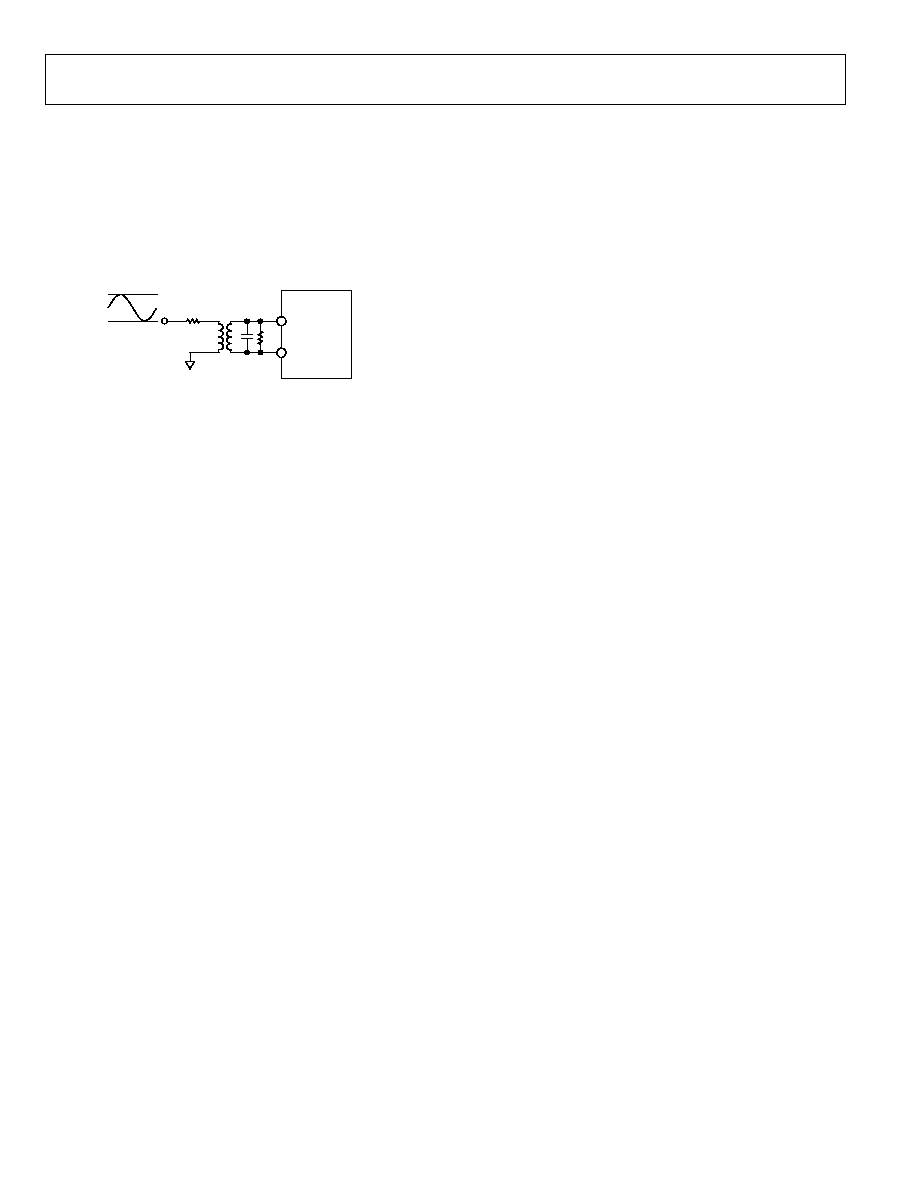
AD9877
Rev. B | Page 32 of 36
Figure 43 shows the schematic of a possible transformer
coupled circuit. Transformers with turn ratios (n
2
/n
1
) other than
1 can be selected to optimize the performance of a given
application. For example, selecting a transformer with a higher
impedance ratio (such as minicircuits T16 to 6T with an
impedance ratio of (z
2
/z
1
) = 16 = (n
2
/n
1
)
2
) effectively steps up
the signal amplitude, thus further reducing the output voltage
swing of the signal source.
AINP
AINN
AD9877
R
R1
C
02716-043
Figure 43. Transformer Coupled Input
In Figure 43, a resistor R1 is added between the analog inputs to
match the source impedance R as in the formula
R = [R1||R
AIN
](Z
1
/Z
2
)
ADC VOLTAGE REFERENCES
The AD9877 has two independent internal references for its
8-bit and 12-bit ADCs. Both 8-bit ADCs have a 1 V p-p input
and share one internal reference source. The 12-bit ADC,
however, is designed for 2 V p-p input voltages and provides its
own internal reference. Figure 16 shows the proper connections
of the reference pins REFT and REFB.
External references may be necessary for systems that require
high accuracy gain matching between ADCs or improvements
in temperature drift and noise characteristics. External
references REFT and REFB need to be centered at AVDD/2
with offset voltages as specified:
REFT8: AVDDIQ/2 + 0.25 V
REFB8: AVDDIQ/2 - 0.25 V
REFT12: AVDD/2 + 0.5 V
REFB12: AVDD/2 - 0.5 V
A differential level of 0.5 V between the reference pins results in
a 1 V p-p ADC input level AIN. A differential level of 1 V
between the reference pins results in a 2 V p-p ADC input level
AIN. Internal reference sources can be powered down when
external references are used (Register Address 0x002).

AD9877
Rev. B | Page 33 of 36
PCB DESIGN CONSIDERATIONS
Although the AD9877 is a mixed-signal device, it should be
treated as an analog component. The on-chip digital circuitry is
specially designed to minimize the impact the digital switching
noise has on the operation of the analog circuits. The power,
grounding, and layout recommendations in this section will
help provide the best performance from the MxFE.
COMPONENT PLACEMENT
Chances for obtaining the best performance from the MxFE are
greatly increased if the three following guidelines of component
placement are followed.
∑
Manage the path of return currents flowing into the ground
plane so that high frequency switching currents from the
digital circuits do not flow onto the ground plane under the
MxFE or analog circuits.
∑
Keep noisy digital signal paths and sensitive receive signal
paths as short as possible.
∑
Keep digital (noise generating) and analog (noise
susceptible) circuits as far away from each other as possible.
To best manage the return currents, pure digital circuits that
generate high switching currents should be closest to the power
supply entry. This keeps the highest frequency return current
paths short and prevents them from traveling over the sensitive
MxFE and analog portions of the ground plane. Also, these
circuits should be generously bypassed at each device, further
reducing the high frequency ground currents. The MxFE
should be placed adjacent to the digital circuits, such that the
ground return currents from the digital sections do not flow
into the ground plane under the MxFE. The analog circuits
should be placed furthest from the power supply.
The AD9877 has several pins that are used to decouple sensitive
internal nodes. These pins are REFIO, REFB8, REFT8, REFB12,
and REFT12. The decoupling capacitors connected to these
points should have low ESR and ESL. These capacitors should
be placed as close as possible to the MxFE and be connected
directly to the analog ground plane.
The resistor connected to the FSADJ pin and the RC network
connected to the PLLFILT pin should also be placed close to the
device and connected directly to the analog ground plane.
POWER PLANES AND DECOUPLING
The AD9877 evaluation board demonstrates a good power
supply distribution and decoupling strategy. The board has four
layers: two signal layers, one ground plane, and one power
plane. The power plane is split into a 3 VDD section used for
the 3 V analog supply pins of the AD9877 and a VANLG
section that supplies the higher voltage analog components on
the board.
That 3 VDD section typically has the highest frequency
currents on the power plane and should be kept the farthest
from the MxFE and analog sections of the board. The DVDD
portion of the plane brings the current used to power the digital
portion of the MxFE to the device. This should be treated
similarly to the 3 VDD power plane and be kept from going
underneath the MxFE or analog components. The MxFE
should sit above the AVDD portion of the power plane.
The AVDD and DVDD power planes can be fed from the same
low noise voltage source. They should be decoupled from each
other, however, to prevent the noise generated in the DVDD
portion of the MxFE from corrupting the AVDD supply. This
can be done by using ferrite beads between the voltage source
and DVDD and between the source and AVDD. Both DVDD
and AVDD should have a low ESR, bulk decoupling capacitor
on the MxFE side of the ferrite as well as low ESR, low ESL
decoupling capacitors on each supply pin (for example, the
AD9877 requires 17 power supply decoupling caps). The
decoupling capacitors should be placed as close as possible to
the MxFE supply pins. An example of the proper decoupling is
shown in the AD9877 evaluation board schematic.
GROUND PLANES
In general, if the component placing guidelines discussed in the
Component Placement section can be implemented, it is best to
have at least one continuous ground plane for the entire board.
All ground connections should be made as short as possible.
This results in the lowest impedance return paths and the
quietest ground connections.
If the components cannot be placed in a manner that keeps the
high frequency ground currents from traversing under the
MxFE and analog components, it may be necessary to put
current steering channels into the ground plane to route the
high frequency currents around these sensitive areas. These
current steering channels should be made only when and where
necessary.

AD9877
Rev. B | Page 34 of 36
SIGNAL ROUTING
The digital Rx and Tx signal paths should be kept as short as
possible. Also, these traces should have a controlled impedance
of about 50 . This prevents poor signal integrity and the high
currents that can occur during undershoot or overshoot caused
by ringing. If the signal traces cannot be kept shorter than
approximately 1.5 inches, then series termination resistors
(33 to 47 ) should be placed close to all signal sources. It is a
good idea to series terminate all clock signals at their source
regardless of trace length.
The receive (I IN, Q IN, and RF IN) signals are the most
sensitive signals on the board. Careful routing of these signals is
essential for good receive path performance. The Rx± signals
form a differential pair and should be routed together as a pair.
By keeping the traces adjacent to each other, noise coupled onto
the signals appears as common-mode and is largely rejected by
the MxFE receive input. Keeping the driving point impedance
of the receive signal low and placing any low-pass filtering of
the signals close to the MxFE further reduces the possibility of
noise corrupting these signals.
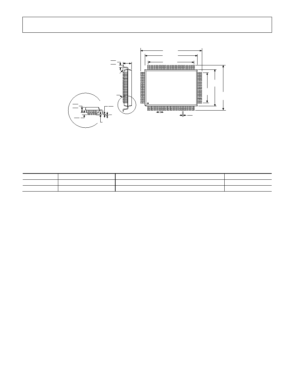
AD9877
Rev. B | Page 35 of 36
OUTLINE DIMENSIONS
81
100
1
50
31
30
51
TOP VIEW
(PINS DOWN)
PIN 1
80
12.35
REF
23.20 BSC
3.40
MAX
20.00 BSC
18.85 REF
14.00
BSC
17.20
BSC
0.40
0.22
0.65 BSC
LEAD PITCH
2.90
2.70
2.50
0.50
0.25
7∞
0∞
0.10
COPLANARITY
VIEW A
ROTATED 90∞ CCW
0.23
0.11
VIEW A
SEATING
PLANE
1.03
0.88
0.73
LEAD WIDTH
COMPLIANT TO JEDEC STANDARDS MS-022-GC-1
Figure 44. 100-Lead Metric Quad Flat Package [MQFP]
(S-100-3)
Dimensions shown in millimeters
ORDERING GUIDE
Model
Temperature Range
Package Description
Package Option
AD9877ABS
-40∞C to +85∞C
100-Lead Metric Quad Flat Package [MQFP]
S-100-3
AD9877-EB
Evaluation
Board

AD9877
Rev. B | Page 36 of 36
NOTES
© 2005 Analog Devices, Inc. All rights reserved. Trademarks and
registered trademarks are the property of their respective owners.
C02716-0-6/05(B)