 | –≠–ª–µ–∫—Ç—Ä–æ–Ω–Ω—ã–π –∫–æ–º–ø–æ–Ω–µ–Ω—Ç: AD9889A | –°–∫–∞—á–∞—Ç—å:  PDF PDF  ZIP ZIP |
Document Outline
- ˛ˇ
- ˛ˇ
- ˛ˇ
- ˛ˇ
- ˛ˇ
- ˛ˇ
- ˛ˇ
- ˛ˇ
- ˛ˇ
- ˛ˇ
- ˛ˇ
- ˛ˇ

High Performance
HDMI/DVI Transmitter
AD9889A
Rev. 0
Information furnished by Analog Devices is believed to be accurate and reliable. However, no
responsibility is assumed by Analog Devices for its use, nor for any infringements of patents or other
rights of third parties that may result from its use. Specifications subject to change without notice. No
license is granted by implication or otherwise under any patent or patent rights of Analog Devices.
Trademarks and registered trademarks are the property of their respective owners.
One Technology Way, P.O. Box 9106, Norwood, MA 02062-9106, U.S.A.
Tel: 781.329.4700
www.analog.com
Fax: 781.461.3113
©2006 Analog Devices, Inc. All rights reserved.
FEATURES
General
HDMI
TM
/DVI transmitter compatible with HDMI v1.2a,
DVI v1.0, and HDCP 1.1
Single 1.8 V power supply
Video/audio inputs accept logic level s from 1.8 V to 3.3 V
76-ball CSP_BGA, Pb-free package
Digital video
80 MHz operation supports all resolutions from 480i to
720p/1080i and XGA-75 Hz
Programmable two-way color space converter
Supports RGB, YCbCr, DDR
Supports ITU656 based embedded syncs
Auto input video format timing detection (CEA-861B)
Digital audio
Supports standard S/PDIF for stereo LPCM or compressed
audio up to 192 kHz
8-channel uncompressed LPCM I
2
S audio up to 192 kHz
Special features for easy system design
On-chip MPU with I
2
CÆ master to perform HDCP
operations and EDID reading operations
5 V tolerant I
2
C and HPD I/Os, no extra device needed
No audio master clock needed for supporting S/PDIF
and I
2
S
On-chip MPU reports HDMI events through interrupts and
registers
APPLICATIONS
DVD players and recorders
Digital set-top boxes
A/V receivers
Digital cameras and camcorders
HDMI repeater/splitter
FUNCTIONAL BLOCK DIAGRAM
SDA
SCL
DDCSDA
DDCSCL
HPD
INT
INTERRUPT
HANDLER
HDCP-EDID
MICRO-
CONTROLLER
HDCP
CORE
I
2
C
MASTER
I
2
C
SLAVE
REGISTER
CONFIGURATION
LOGIC
HDMI
Tx
CORE
XOR
MASK
COLOR
SPACE
CONVER-
SION
4:2:2 TO
4:4:4
CONVER-
SION
VIDEO
DATA
CAPTURE
AUDIO
DATA
CAPTURE
Tx0[1:0]
Tx1[1:0]
Tx2[1:0]
TxC[1:0]
CLK
VSYNC
HSYNC
DE
D[23:0]
S/PDIF
MCLK
I
2
S[3:0]
LRCLK
SCLK
MDA
MCL
AD9889A
061
48-
0
01
Figure 1.
GENERAL DESCRIPTION
The AD9889A-BBCZ is an 80 MHz, high definition multimedia
interface (HDMI) v.1.2a transmitter. It supports HDTV formats
up to 720p/1080i, and computer graphic resolutions up to XGA
(1024 ◊ 768 @ 75 Hz). With the inclusion of HDCP, the AD9889A
allows the secure transmission of protected content as specified
by the HDCP v1.1 protocol.
The AD9889A supports both S/PDIF and 8-channel I
2
S audio.
Its high fidelity 8-channel I
2
S can transmit either stereo or 7.1
surround audio at 192 kHz. The S/PDIF can carry stereo
LPCM audio or compressed audio including DolbyÆ Digital,
DTSÆ, and THXÆ.
The AD9889A helps to reduce system design complexity and
cost by incorporating such features as an internal MPU for
HDCP operations, an I
2
C master for EDID reading, a single
1.8 V power supply and 5 V tolerance on I
2
C and hot plug
detect pins.
Fabricated in an advanced CMOS process, the AD9889A
is available in a space saving, 76-ball, CSP_BGA surface-
mount package. The CSP_BGA package is specified from
-25∞C to +90∞C.

AD9889A
Rev. 0 | Page 2 of 12
TABLE OF CONTENTS
Features .............................................................................................. 1
Applications....................................................................................... 1
Functional Block Diagram .............................................................. 1
General Description ......................................................................... 1
Revision History ............................................................................... 2
Specifications..................................................................................... 3
Absolute Maximum Ratings............................................................ 4
Explanation of Test Levels ........................................................... 4
ESD Caution.................................................................................. 4
Pin Configuration and Function Descriptions............................. 5
Applications........................................................................................7
Design Resources ..........................................................................7
Document Conventions ...............................................................7
PCB Layout Recommendations.......................................................8
Power Supply Bypassing ...............................................................8
Digital Inputs .................................................................................8
External Swing Resistor................................................................8
Output Signals ...............................................................................8
Outline Dimensions ..........................................................................9
Ordering Guide..............................................................................9
REVISION HISTORY
10/06--Revision 0: Initial Version

AD9889A
Rev. 0 | Page 3 of 12
SPECIFICATIONS
Table 1.
Parameter Conditions
Temp
Test
Level
1
Min
Typ Max Unit
DIGITAL INPUTS
Input Voltage, High (V
IH
)
Full
VI
1.4
V
Input Voltage, Low (V
IL
)
Full
VI
0.7
V
Input Capacitance
25∞C
V
3
pF
DIGITAL OUTPUTS
Output Voltage, High (V
OH
)
Full
VI
V
DD
- 0.1
V
Output Voltage, Low (V
OL
)
Full
VI
0.4
V
THERMAL CHARACTERISTICS
Thermal Resistance
JC
Junction-to-Case
V
15.2
∞C/W
JA
Junction-to-Ambient
V
59
∞C/W
Ambient Temperature
Full
V
-25
+25
+90
∞C
DC SPECIFICATIONS
Input Leakage Current, I
IL
25∞C
VI
-10
+10
A
Input Clamp Voltage
-16 mA
25∞C
V
-0.8
V
+16
mA
25∞C
V
+0.8
V
Differential High Level Output Voltage
V
AV
CC
V
Differential Output Short-Circuit Current
IV
10
A
POWER SUPPLY
V
DD
(All) Supply Voltage
Full
IV
1.71
1.8
1.89
V
V
DD
Supply Voltage Noise
Full
V
50
mV p-p
Power-Down Current
With active video applied
25∞C
IV
9
mA
Transmitter Supply Current
2
80 MHz, typical random pattern
25∞C
IV
143
155
mA
Transmitter Total Power
Full
VI
257
280
mW
AC SPECIFICATIONS
CLK Frequency
25∞C
IV
13.5
80
MHz
TMDS Output CLK Duty Cycle
25∞C
IV
48
52
%
Worst Case CLK Input Jitter
Full
IV
2
ns
Input Data Setup Time
Full
IV
1
ns
Input Data Hold Time
Full
IV
1
ns
TMDS Differential Swing
VI
800
1000
1200
mV
V
SYNC
and H
SYNC
Delay from DE Falling Edge
VI
1
UI
3
V
SYNC
and H
SYNC
Delay to DE Rising Edge
VI
1
UI
DE High Time
25∞C
VI
8191
UI
DE Low Time
25∞C
VI
138
UI
Differential Output Swing
Low-to-High Transition Time
25∞C
VII
75
490
ps
High-to-Low Transition Time
25∞C
VII
75
490
ps
AUDIO AC TIMING
Sample Rate
I
2
S and S/PDIF
Full
IV
32
192
kHz
I
2
S Cycle Time
25∞C
IV
1
UI
I
2
S Setup Time
25∞C
IV
15
ns
I
2
S Hold Time
25∞C
IV
0
ns
Audio Pipeline Delay
25∞C
IV
75
s
1
See Explanation of Test Levels section.
2
Using low output drive strength.
3
UI = unit interval.
AD9889A
Rev. 0 | Page 4 of 12
ABSOLUTE MAXIMUM RATINGS
Table 2.
Parameter Rating
Digital Inputs
5 V to 0.0 V
Digital Output Current
20 mA
Operating Temperature Range
-40∞C to +90∞C
Storage Temperature Range
-65∞C to +150∞C
Maximum Junction Temperature
150∞C
Maximum Case Temperature
150∞C
Stresses above those listed under Absolute Maximum Ratings
may cause permanent damage to the device. This is a stress
rating only; functional operation of the device at these or any
other conditions above those indicated in the operational
section of this specification is not implied. Exposure to absolute
maximum rating conditions for extended periods may affect
device reliability.
EXPLANATION OF TEST LEVELS
I.
100% production tested.
II.
100% production tested at 25∞C and sample tested at
specified temperatures.
III. Sample
tested
only.
IV.
Parameter is guaranteed by design and characterization
testing.
V.
Parameter is a typical value only.
VI.
100% production tested at 25∞C; guaranteed by design
and characterization testing.
VII.
Limits defined by HDMI specification; guaranteed by
design and characterization testing.
ESD CAUTION

AD9889A
Rev. 0 | Page 5 of 12
PIN CONFIGURATION AND FUNCTION DESCRIPTIONS
0
61
48
-
0
04
A
B
C
D
E
F
G
J
H
K
10
8 7 6
3 2 1
9
5 4
BOTTOM VIEW
(Not to Scale)
Figure 2. 76-Ball BGA Configuration (Top View)
Table 3. Pin Function Descriptions
Pin No.
Mnemonic
Type
1
Description
A1 to A10, B1
to B10, C9,
C10, D9, D10
D[23:0]
I
Video Data Input. Digital input in RGB or YCbCr format. Supports CMOS logic levels from 1.8 V to 3.3 V.
D1
CLK
I
Video Clock Input. Supports CMOS logic levels from 1.8 V to 3.3 V.
C2
DE
I
Data Enable Bit for Digital Video. Supports CMOS logic levels from 1.8 V to 3.3 V.
C1
HSYNC
I
Horizontal SYNC Input. Supports CMOS logic levels from 1.8 V to 3.3 V.
D2
VSYNC
I
Vertical SYNC Input. Supports CMOS logic levels from 1.8 V to 3.3 V.
J3
EXT_SW
I
Sets internal reference currents. Place 887 resistor (1% tolerance) between this pin and ground.
K3 HPD
I
Hot Plug Detect Signal. This indicates to the interface whether the receiver is connected. 1.8 V to
5.0 V CMOS logic level.
E2 S/PDIF
I
S/PDIF (Sony/Philips Digital Interface) Audio Input. This is the audio input from a Sony/Philips
digital interface. Supports CMOS logic levels from 1.8 V to 3.3 V.
E1 MCLK
I
Audio Reference Clock. 128 ◊ N ◊ f
S
with N = 1, 2, 3, or 4. Set to 128 ◊ sampling frequency (f
S
),
256 ◊ f
S
, 384 ◊ f
S
, or 512 ◊ f
S
. 1.8 V to 3.3 V CMOS logic level.
F2, F1, G2, G1
I
2
S[3:0] I I
2
S Audio Data Inputs. These represent the eight channels of audio (two per input) available
through I
2
S. Supports CMOS logic levels from 1.8 V to 3.3 V.
H2 SCLK
I
I
2
S Audio Clock. Supports CMOS logic levels from 1.8 V to 3.3 V.
H1
LRCLK
I
Left/Right Channel Selection. Supports CMOS logic levels from 1.8 V to 3.3 V.
J7 PD/A0
I
Power-Down Control and I
2
C Address Selection. The I
2
C address and the PD polarity are set by the
PD/A0 pin state when the supplies are applied to the AD9889A. 1.8 V to 3.3 V CMOS logic level.
K1, K2
TxC-/TxC+
O
Differential Clock Output. Differential clock output at pixel clock rate; transition minimized
differential signaling (TMDS) logic level.
K10, J10
Tx2-/Tx2+
O
Differential Output Channel 2. Differential output of the red data at 10◊ the pixel clock rate; TMDS
logic level.
K7, K8
Tx1-/Tx1+
O
Differential Output Channel 1. Differential output of the green data at 10◊ the pixel clock rate;
TMDS logic level.
K4, K5
Tx0-/Tx0+
O
Differential Output Channel 0. Differential output of the blue data at 10◊ the pixel clock rate; TMDS
logic level.
H10 INT
O
Interrupt. CMOS logic level. A 2 k pull up resistor to interrupt the microcontroller IO supply is
recommended.
J2, J5, J8, K9
AVDD
P
1.8 V Power Supply for TMDS Outputs.
D5, D6, D7, E7
DVDD
P
1.8 V Power Supply for Digital and I/O Power Supply. These pins supply power to the digital logic
and I/Os. They should be filtered and as quiet as possible.
G4, G5, J1
PVDD
P
1.8 V PLL Power Supply. The most sensitive portion of the AD9889A is the clock generation
circuitry. These pins provide power to the clock PLL. The designer should provide quiet, noise-free
power to these pins.
D4, E4, F4, J4,
G6, J6, K6, F7,
G7, H9, J9
GND P
Ground. The ground return for all circuitry on-chip. It is recommended that the AD9889A be
assembled on a single, solid ground plane with careful attention given to ground current paths.
AD9889A
Rev. 0 | Page 6 of 12
Pin No.
Mnemonic
Type
1
Description
F9 SDA
C
2
Serial Port Data I/O. This pin serves as the serial port data I/O slave for register access. Supports
CMOS logic levels from 1.8 V to 3.3 V.
F10 SCL
C
2
Serial Port Data Clock. This pin serves as the serial port data clock slave for register access. Supports
CMOS logic levels from 1.8 V to 3.3 V.
E10 MDA
C
2
Serial Port Data I/O Master to HDCP Key EEPROM. Supports CMOS logic levels from 1.8 V to 3.3 V.
E9 MCL
C
2
Serial Port Data Clock Master to HDCP Key EEPROM. Supports CMOS logic levels from 1.8 V to 3.3 V.
G9 DDCSDA
C
2
Serial Port Data I/O to Receiver. This pin serves as the master to the DDC bus. 5 V CMOS logic level.
G10 DDCSCL
C
2
Serial Port Data Clock to Receiver. This pin serves as the master clock for the DDC bus. 5 V CMOS
logic level.
1
I = input, O = output, P = power supply, C = control.
2
For a full description of the 2-wire serial interface and its functionality obtain documentation by contacting NDA from flatpanel_apps@analog.com.

AD9889A
Rev. 0 | Page 7 of 12
APPLICATIONS
DESIGN RESOURCES
Analog Devices, Inc. evaluation kits, reference design
schematics, and other support documentation is available under
NDA from flatpanel_apps@analog.com.
Other resources include:
EIA/CEA-861B that describes audio and video infoframes as
well as the E-EDID structure for HDMI. It is available from
Consumer Electronics Association (CEA).
The HDMI v1.2a, a defining document for HDMI Version 1.2a,
and the HDMI Compliance Test Specification Version 1.2a are
available from HDMI Licensing, LLC.
The HDCP v1.1 is the defining document for HDCP
Version 1.1. available from Digital Content Protection, LLC.
DOCUMENT CONVENTIONS
In this data sheet, data is represented using the conventions
described in Table 4.
Table 4. Document Conventions
Data
Type Format
0xNN
Hexadecimal (Base-16) numbers are represented using
the C language notation, preceded by 0x.
0bNN
Binary (Base-2) numbers are represented using the C
language notation, preceded by 0b.
NN
Decimal (Base-10) numbers are represented using no
additional prefixes or suffixes.
Bit
Bits are numbered in little endian format, that is, the
least significant bit of a byte or word is referred to as Bit 0.

AD9889A
Rev. 0 | Page 8 of 12
PCB LAYOUT RECOMMENDATIONS
The AD9889A is a high precision, high speed analog device. As
such, to get the maximum performance out of the part, it is
important to have a well laid out board.
POWER SUPPLY BYPASSING
It is recommended to bypass each power supply pin with a
0.1 F capacitor. The exception is when two or more supply
pins are adjacent to each other. For these groupings of
powers/grounds, it is necessary to have only one bypass
capacitor. The fundamental idea is to have a bypass capacitor
within about 0.5 cm of each power pin. Also, avoid placing the
capacitor on the opposite side of the PC board from the
AD9889A, as that interposes resistive vias in the path.
The bypass capacitors should be physically located between the
power plane and the power pin. Current should flow from the
power plane to the capacitor to the power pin. Do not make a
power connection between the capacitor and the power pin.
Placing a via underneath the capacitor pads, down to the power
plane, is generally the best approach.
It is particularly important to maintain low noise and good
stability of PVDD (the PLL supply). Abrupt changes in PVDD
can result in similarly abrupt changes in sampling clock phase
and frequency. This can be avoided by careful attention to
regulation, filtering, and bypassing. It is best practice to provide
separate regulated supplies for each of the analog circuitry
groups (AVDD and PVDD).
It is also recommended to use a single ground plane for
the entire board. Experience has repeatedly shown that
the noise performance is the same or better with a single
ground plane. Using multiple ground planes can be detri-
mental because each separate ground plane is smaller, and
long ground loops can result.
DIGITAL INPUTS
Video and Audio Data Input Signals
The digital inputs on the AD9889A are designed to work with
signals ranging from 1.8 V to 3.3 V logic level. Therefore, no
extra components need to be added when using 3.3 V logic.
Any noise that gets onto the clock input (labeled CLK) trace
adds jitter to the system. Therefore, minimize the video clock
input (Pin 6: CLK) trace length and do not run any digital or
other high frequency traces near it. Make sure to match the
length of the input data signals to optimize data capture,
especially for high frequency modes (such as 720p or XGA
75 MHz) and double data rate input formats.
Other Input Signals
The HPD must be connected to the HDMI connector. A 10 k
pull-down resistor to ground is also recommended.
The PD/A0 input pin can be connected to GND or supply
(through a resistor or a control signal). The device address and
power-down polarity are set by the state of the PD/A0 pin when
the AD9889A supplies are applied/enabled. For example, if the
PD/A0 pin is low (when the supplies are turned on), then the
device address is 0x72 and the power down is active high. If the
PD/A0 pin is high (when the supplies are turned on), the device
address is 0x7A and the power down is active low.
The SCL and SDA pins should be connected to the I
2
C master.
A pull-up resistor of 2 k to 1.8 V or 3.3 V is recommended.
EXTERNAL SWING RESISTOR
The external swing resistor must be connected directly to the
EXT_SWG pin and ground. The external swing resistor must
have a value of 887 (±1% tolerance). Avoid running any high
speed ac or noisy signals next to, or close to, the EXT_SWG pin.
OUTPUT SIGNALS
TMDS Output Signals
The AD9889A has three TMDS data channels (0, 1, and 2) that
output signals up to 800 MHz as well as the TMDS output data
clock. To minimize the channel-to-channel skew, make the
trace length of these signals the same. Also, these traces need to
have a 50 characteristic impedance and routed as 100
differential pairs. It is also recommended to route these lines on
the top PCB layer avoiding the use of vias.
Other Output Signals (non TMDS)
DDCSCL and DDCSDA
The DDCSCL and DDCSDA outputs need to have a minimum
amount of capacitance loading to ensure the best signal integrity.
The DDCSCL and DDCSDA capacitance loading must be less
than 50 pF to meet the HDMI compliance specification. The
DDCSCL and DDCSDA must be connected to the HDMI
connector and a pull-up resistor to 5 V is required. The pull-up
resistor must have a value between 1.5 k and 2 k.
INT Pin
The INT pin is an output that should be connected to the
microcontroller of the system. A pull-up resistor to 1.8 V or
3.3 V is required for proper operation: the recommended value
is 2 k.
MCL and MDA
The MCL and MDA outputs should be connected to the
EEPROM containing the HDCP key (if HDCP is implemented).
Pull-up resistors of 2 k are recommended.
AD9889A
Rev. 0 | Page 9 of 12
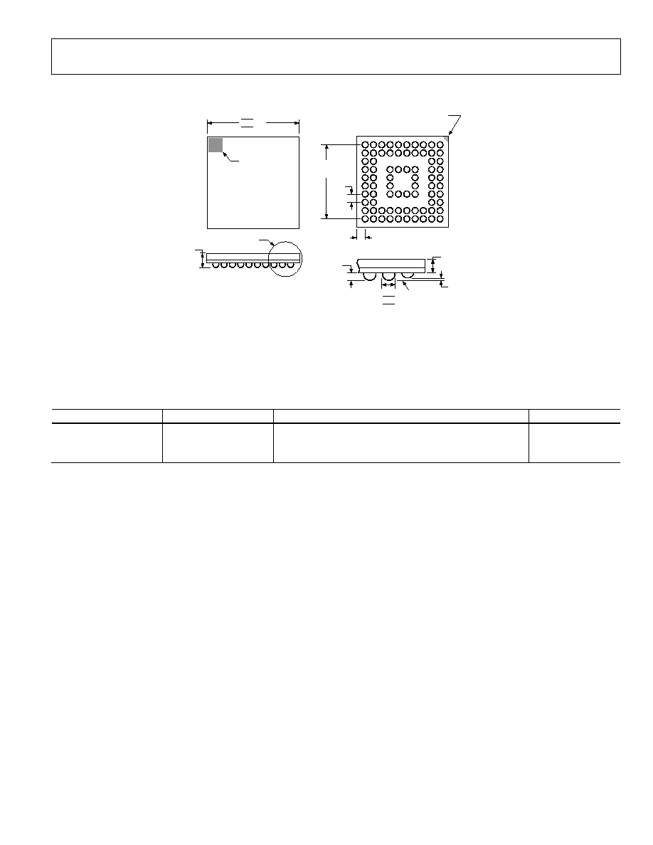
OUTLINE DIMENSIONS
*COMPLIANT TO JEDEC STANDARDS MO-225
WITH THE EXCEPTION TO PACKAGE HEIGHT.
A
B
C
D
E
F
G
J
H
K
10
8 7 6
3 2 1
9
5 4
A1 CORNER
INDEX AREA
TOP VIEW
BALL A1
PAD CORNER
DETAIL A
BOTTOM VIEW
0.75
REF
6.10
6.00 SQ
5.90
SEATING
PLANE
DETAILA
BALL DIAMETER
0.15 MIN
0.35
0.30
0.25
COPLANARITY
0.08 MAX
0.65 MIN
0.50
BSC
4.50
BSC SQ
*1.40 MAX
01
20
06
-
0
Figure 3. 76-Ball Chip Scale Package Ball Grid Array [CSP_BGA]
6 mm ◊ 6 mm ◊ 1.4 mm
(BC-76)
Dimensions shown in millimeters
ORDERING GUIDE
Model
Temperature Range
Package Description
Package Option
AD9889ABBCZ-80
1
-25∞C to +90∞C
76-Ball Chip Scale Package Ball Grid Array [CSP_BGA]
BC-76
AD9889ABBCZRL-80
1
-25∞C to +90∞C
76-Ball Chip Scale Package Ball Grid Array [CSP_BGA]
BC-76
AD9889A/PCB
Evaluation
Board
1
Z = Pb-free part.

AD9889A
Rev. 0 | Page 10 of 12
NOTES

AD9889A
Rev. 0 | Page 11 of 12
NOTES

AD9889A
Rev. 0 | Page 12 of 12
NOTES
Purchase of licensed I
2
C components of Analog Devices or one of its sublicensed Associated Companies conveys a license for the purchaser under the Philips I
2
C Patent
Rights to use these components in an I
2
C system, provided that the system conforms to the I
2
C Standard Specification as defined by Philips.
©2006 Analog Devices, Inc. All rights reserved. Trademarks and
registered trademarks are the property of their respective owners.
D06148-0-10/06(0)