 | –≠–ª–µ–∫—Ç—Ä–æ–Ω–Ω—ã–π –∫–æ–º–ø–æ–Ω–µ–Ω—Ç: ADD8754 | –°–∫–∞—á–∞—Ç—å:  PDF PDF  ZIP ZIP |
Document Outline
- FEATURES
- APPLICATIONS
- GENERAL DESCRIPTION
- FUNCTIONAL BLOCK DIAGRAM
- SPECIFICATIONS
- ˛ˇ
- ˛ˇ
- ˛ˇ
- ˛ˇ
- ˛ˇ
- ˛ˇ
LCD Panel Power, V
COM
,
and
G
ate Modulation
ADD8754
Rev. 0
Information furnished by Analog Devices is believed to be accurate and reliable.
However, no responsibility is assumed by Analog Devices for its use, nor for any
infringements of patents or other rights of third parties that may result from its use.
Specifications subject to change without notice. No license is granted by implication
or otherwise under any patent or patent rights of Analog Devices. Trademarks and
registered trademarks are the property of their respective owners.
One Technology Way, P.O. Box 9106, Norwood, MA 02062-9106, U.S.A.
Tel: 781.329.4700
www.analog.com
Fax: 781.461.3113
©2005 Analog Devices, Inc. All rights reserved.
FEATURES
Step-up switching regulator with 2 A power switch
650 kHz or 1.2 MHz switching frequency
Output adjustable to 20 V
350 mA logic voltage regulator
Selectable output voltages: 2.5 V, 2.85 V, 3.3 V
V
COM
amplifier with 300 mA drive
Gate pulse modulation circuitry
Independently adjustable delay and falling slope
General
3 V to 5.5 V input
Undervoltage lockout
Thermal shutdown
24-lead, Pb-free LFCSP package
APPLICATIONS
TFT LCD panels for monitors, TVs, and notebooks
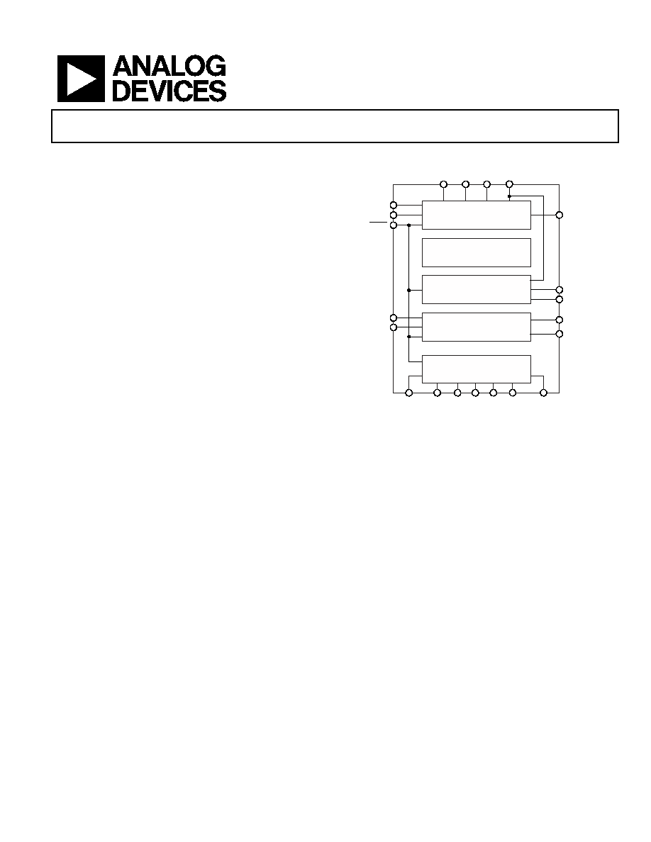
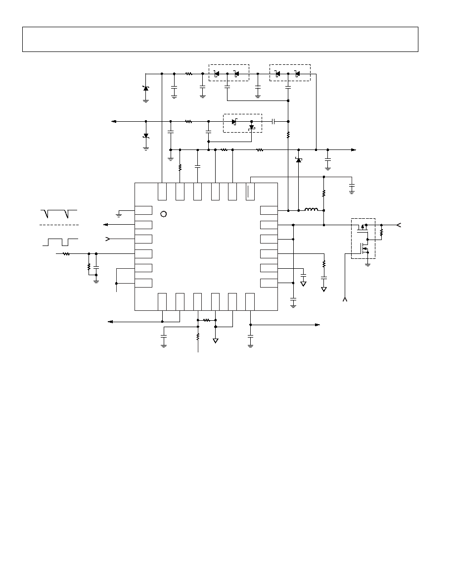
FUNCTIONAL BLOCK DIAGRAM
ADD8754
VGH
VGH_M VDD_1 CE RE VFLK
VDPM
05110-001
GATE PULSE
MODULATION
VCOM AMPLIFIER
LOGIC VOLTAGE
REGULATOR
UNDER VOLTAGE LOCKOUT
AND THERMAL PROTECTION
FB
FREQ
SHDN
VDD_2
OUT
STEP-UP SWITCHING
REGULATOR
VIN_2
VIN_1
SS
COMP
LDO_OUT
ADJ
LX
POS
NEG
Figure 1.
GENERAL DESCRIPTION
The ADD8754 is optimized for use in TFT LCD applications,
requiring only external charge pump components to provide all
the requirements for panel power, V
COM
, and gate modulation.
Included in a single chip are a high frequency step-up dc-to-dc
switching regulator, logic voltage regulator, V
COM
amplifier, and
gate pulse modulation circuitry.
The step-up dc-to-dc converter provides up to 20 V output and
includes a 2 A internal switch. Either a 650 kHz or 1.2 MHz step-
up switching regulator frequency can be chosen, allowing easy
filtering and low noise operation. It achieves 93% efficiency and
features soft start to limit the inrush current at startup.
The internal voltage regulator operates with an input voltage
range of 3 V to 5.5 V and delivers a load current of up to
350 mA. Three selectable output voltages are available: 2.5 V,
2.85 V, and 3.3 V.
The proprietary V
COM
amplifier can deliver a peak output
current of 300 mA and is specifically designed to drive TFT
panel loads.
The gate pulse modulator allows shaping of the TFT gate high
voltage to improve image quality. The integrated switches
provide the ability to independently control the delay and slope
for the gate drive voltage.
The ADD8754 is offered in a 24-lead, Pb-free LFCSP package and
is specified over the industrial temperature range of -40 to +85∞C.

ADD8754
Rev. 0 | Page 2 of 28
TABLE OF CONTENTS
Specifications..................................................................................... 3
Step-Up Switching Regulator Specifications............................. 3
LDO Regulator Specifications .................................................... 4
V
COM
Amplifier Specifications .................................................... 5
Gate Pulse Modulator Specifications ......................................... 6
General Specifications ................................................................. 6
Absolute Maximum Ratings............................................................ 7
ESD Caution.................................................................................. 7
Pin Configuration and Function Descriptions............................. 8
Typical Performance Characteristics ............................................. 9
Theory of Operation ...................................................................... 12
Current-Mode, Step-Up Switching Regulator Operation..... 12
V
COM
Amplifier ........................................................................... 16
Gate Pulse Modulator Circuit................................................... 16
Power-Up Sequence ................................................................... 17
Shutdown..................................................................................... 17
UVLO........................................................................................... 17
Power Dissipation....................................................................... 18
Layout Guidelines....................................................................... 19
Typical Application Circuits ......................................................... 20
Outline Dimensions ....................................................................... 25
Ordering Guide .......................................................................... 25
REVISION HISTORY
4/05--Revision 0: Initial Version
ADD8754
Rev. 0 | Page 3 of 28
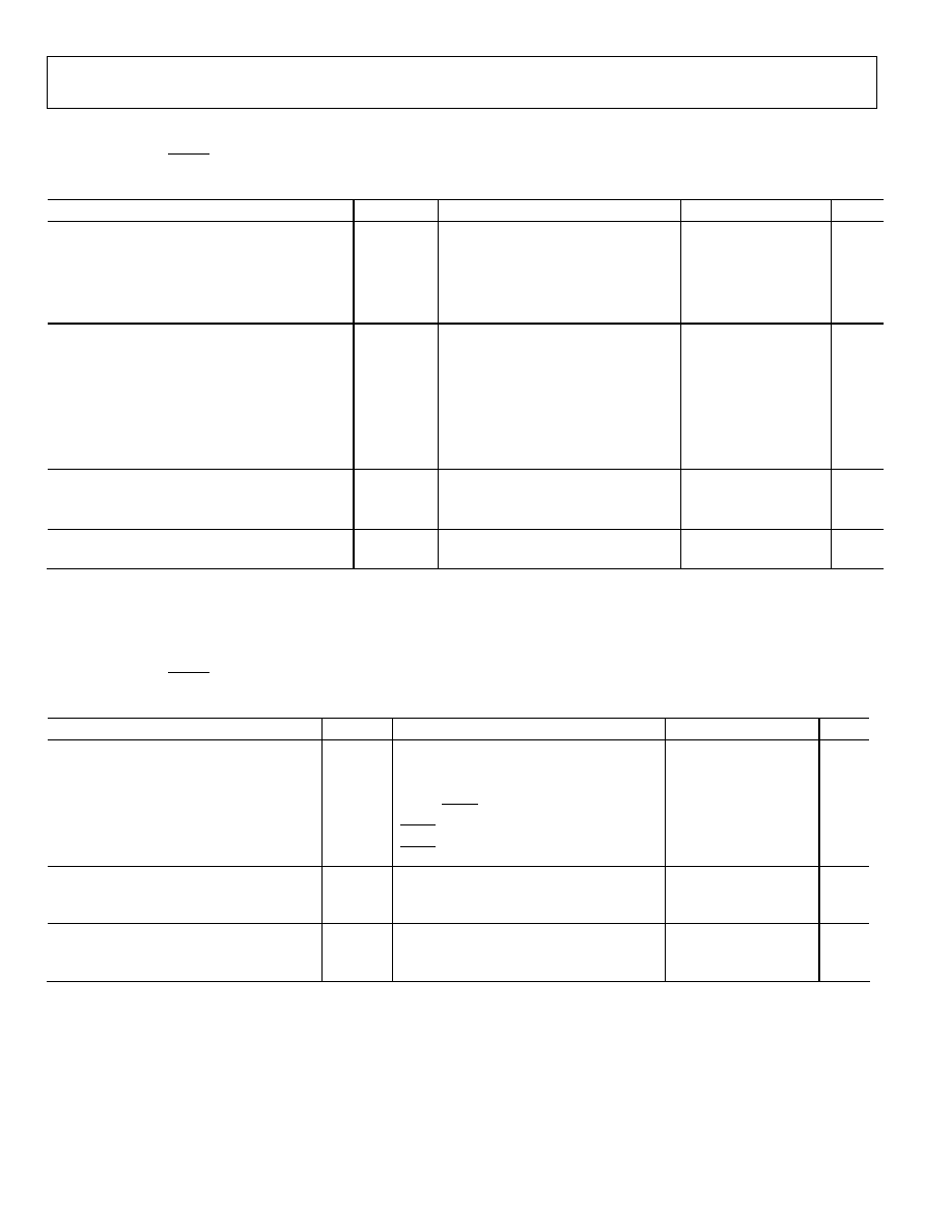
SPECIFICATIONS
STEP-UP SWITCHING REGULATOR SPECIFICATIONS
VIN_1 = VIN_2 = SHDN = 5 V, V
OUT
1
= VDD_1 = VDD_2 = 14 V, T
A
= 25∞C, FREQ = GND, unless otherwise noted.
Table 1.
Parameter
Symbol
Conditions
Min
Typ
Max
Unit
SUPPLY
Input Voltage Range
VIN
3.0
5.5
V
OUTPUT
1
Output Voltage Range
V
OUT
1
20
V
Load Regulation
10 mA I
LOAD
150 mA, V
OUT
1
= 10 V
200
V/mA
Line Regulation
I
LOAD
= 350 mA, 4.5 V VIN_1 5.5 V
mV
Load Regulation
10 mA I
LOAD
150 mA, V
OUT
1
= 10 V
200
V/mA
Line Regulation
I
LOAD
= 150 mA, 3.0 V VIN_1 5.5 V
mV
Overall Regulation
Line, load, temperature (-40∞C T
A
+85∞C)
-3
+3
%
REFERENCE
Feedback Voltage
VFB
1.200
1.211
1.220
V
ERROR AMPLIFIER
Transconductance G
MEA
100
A/V
Gain A
V
1000
V/V
Input Bias Current
I
B
225
nA
SWITCH
On Resistance
R
DS (ON)
170
m
Leakage Current
I
LKG
V
LX
= 14 V, SHDN = GND
0.5
A
Peak Current Limit
I
CL
2.6
A
OSCILLATOR
Oscillator Frequency
F
OSC
FREQ = GND
650
kHz
FREQ = VIN_1
1.2
MHz
Maximum Duty Cycle
D
MAX
VFB = 1 V
90
95
%
SOFT START
Peak Current
SS = GND
2.5
A
1
Refer to the Figure 23.
ADD8754
Rev. 0 | Page 4 of 28
LDO REGULATOR SPECIFICATIONS
VIN_1 = VIN_2 = SHDN = 5 V, ADJ = LDO_OUT,
1
CLDO = 2.2 F, T
A
= 25∞C, unless otherwise noted.
Table 2.
Parameter
Symbol
Conditions
Min
Typ
Max
Unit
INPUT
Input Voltage Range
VIN
2
ADJ = LDO_OUT
1
3.0 5.5
V
ADJ = OPEN
3
3.35 5.5 V
ADJ = GND
4
3.8 5.5
V
OUTPUT
Output Voltage
LDO_OUT
I
LDO
= 1 mA, ADJ = GND
3.31
V
I
LDO
= 350 mA, ADJ = GND
3.29
V
I
LDO
= 1 mA, ADJ = OPEN
2.86
V
I
LDO
= 350 mA, ADJ = OPEN
2.84
V
I
LDO
= 1 mA, ADJ = LDO_OUT
2.51
V
I
LDO
= 350 mA, ADJ = LDO_OUT
2.49
V
Voltage Accuracy
I
LDO
= 1 mA to 350 mA, -40∞C T
A
+85∞C
-3
+3
%
Line Regulation
I
LDO
= 1 mA
3
mV/V
Load Regulation
I
LDO
= 1 mA to 350 mA
20
mV
Dropout Voltage
V
DROP
LDO_OUT = 98% of LDO_OUT(NOM), I
LDO
= 350 mA
300
500
mV
Current Limit
I
LDPK
350
mA
1
Sets LDO_OUT(NOM) to 2.5 V.
2
VIN = VIN_1 = VIN_2.
3
Sets LDO_OUT(NOM) to 2.85 V.
4
Sets LDO_OUT(NOM) to 3.3 V.
ADD8754
Rev. 0 | Page 5 of 28
V
COM
AMPLIFIER SPECIFICATIONS
VIN_1 = VIN_2 = SHDN = 5 V, VDD_2 = 14 V, POS = 4.0 V, NEG = OUT, T
A
= 25∞C, unless otherwise noted.
Table 3.
Parameter Symbol
Conditions
Min
Typ
Max
Unit
INPUT CHARACTERISTICS
Offset Voltage
V
OS
19
mV
Noninverting Input Bias Current
I
B
50
300
nA
Input Voltage Range
2
VDD_2 - 3
V
Common-Mode Rejection Ratio
CMRR
V
CM
= 2 V to (VDD_2 - 3) V
60
dB
OUTPUT CHARACTERISTICS
Output Voltage Swing
V
OH
I
OUT
(source) = 50 mA
VDD_2 - 0.5
V
V
OL
I
OUT
(sink) = 50 mA
50
mV
Output Current
1
I
OUT
±300
mA
POWER SUPPLY
Supply Voltage
VDD_2
8
18
V
Power Supply Rejection Ratio
PSRR
7.5 V VDD_2 18.5 V
65 70
dB
Supply Current
I
SY
No load, POS = VDD_2 /2
2
mA
DYNAMIC PERFORMANCE
Slew Rate
2
SR R
L
= 10 k, C
L
= 10 pF
105
V/s
Gain Bandwidth
GBW
-3 dB, R
L
= 10 k, C
L
= 10 pF
1.95
MHz
1
Not short-circuit protected.
2
Slew rate is the average of the rising and the falling slew rates.
ADD8754
Rev. 0 | Page 6 of 28
GATE PULSE MODULATOR SPECIFICATIONS
VIN_1 = VIN_2 = SHDN = 5 V, VGH = 20 V, VDD_1 = 14 V, T
A
= 25∞C, unless otherwise noted.
Table 4.
Parameter
Symbol
Condition
Min
Typ
Max
Unit
INPUT CHARACTERISTICS
VGH Voltage
VGH
7
30
V
VGH Input Current
I
VGH
VFLK = GND, VDPM = LDO_OUT
95
A
VDD_1 Voltage
7
VGH
V
VDD_1 Input Current
I
VDD_1
VFLK = VDPM = LDO_OUT
0.02
A
CONTROL INPUT CHARACTERISTICS
VFLK Voltage Low
V
LOWFLK
0.8
V
VFLK Voltage High
V
HIGHFLK
2.2
V
VFLK Input Current
I
FLK
0.9 VFLK LDO_OUT
-1
+1
A
VDPM Voltage Low
V
LOWDPM
0.8
V
VDPM Voltage High
V
HIGHDPM
2.2
V
VDPM Input Current
I
VDPM
0.9 VDPM LDO_OUT
-1
+1
A
SWITCHING CHARACTERISTICS
VGH to VGH_M On Resistance
R
VGH
VDPM
= VFLK = LDO_OUT
60
VGH_M Discharge Current
1
I
VGH_M
VFLK < 0.8 V, RE = 33 k
8.0
mA
DELAY CHARACTERISTICS
Delay Time
2
T
DELAY
CE = 470 pF, RE = 33 k
1.88
s
1
Discharge current = 302.5/(RE + 5000).
2
Delay time = CE ◊ 4200.
GENERAL SPECIFICATIONS
VIN_1 = VIN_2 = SHDN = 5 V, T
A
= 25∞C, unless otherwise noted.
Table 5.
Parameter
Symbol
Conditions
Min
Typ
Max
Unit
SHUTDOWN
Input Voltage Low
V
IL
0.8
V
Input Voltage High
V
IH
2.2
V
Shutdown Pin Input Current
GND SHDN 5.5 V
-1 +1 A
Total Ground Current
SHDN = GND
2.0
A
Total V
IN
Current (I
VIN_1
+ I
VIN_2
)
SHDN = GND
-1 +1 A
UNDERVOLTAGE LOCKOUT
UVLO Rising Threshold
V
UVLOR
VIN_1 rising
2.8
V
UVLO Falling Threshold
V
UVLOF
VIN_1 falling
2.6
V
QUIESCENT CURRENT
Step-Up Regulator in Nonswitching State
I
Q
300
500
A
Step-Up Regulator in Switching State
I
QSW
2
3
mA

ADD8754
Rev. 0 | Page 7 of 28
ABSOLUTE MAXIMUM RATINGS
T = 25∞C, unless otherwise noted.
A
Table 6.
Parameter Symbol
Rating
Stresses above those listed under Absolute Maximum Ratings
may cause permanent damage to the device. This is a stress
rating only; functional operation of the device at these or any
other conditions above those indicated in the operational
section of this specification is not implied. Exposure to absolute
maximum rating conditions for extended periods may affect
device reliability.
RE, CE, FB, SHDN
, VIN_2, FREQ,
COMP, SS, VIN_1, LDO_OUT,
ADJ, VDPM, VFLK to GND,
PGND, and AGND
-0.5 V to +6.5 V
-0.5 V to +16 V
OUT, NEG and POS to GND,
PGND, and AGND
LX to GND, PGND, and AGND
-0.5 V to +22 V
VDD_2 and OUT to GND, PGND,
and AGND
-0.5 V to +18.5
V
Absolute maximum ratings apply individually only, not in
combination.
±0.5
V
Voltage Between GND and
AGND, GND and PGND, and
AGND and PGND
-0.5 V to +32 V
VDD_1, VGH, and VGH_M to
GND, PGND, and AGND
±5
V
Differential Voltage Between
POS and NEG
Package Power Dissipation
P
D
(T
J
max - T
A
)/
JA
Thermal Resistance
JA
38∞C/W
Maximum Junction Temperature T
J
max
125∞C
Operating Temperature Range
T
A
-40∞C to +85∞C
Storage Temperature Range
T
S
-65∞C to +150∞C
250∞C
Reflow Peak Temperature
(20 sec to 40 sec)
ESD CAUTION
ESD (electrostatic discharge) sensitive device. Electrostatic charges as high as 4000 V readily accumulate on
the human body and test equipment and can discharge without detection. Although this product features
proprietary ESD protection circuitry, permanent damage may occur on devices subjected to high energy
electrostatic discharges. Therefore, proper ESD precautions are recommended to avoid performance
degradation or loss of functionality.

ADD8754
Rev. 0 | Page 8 of 28
PIN CONFIGURATION AND FUNCTION DESCRIPTIONS
24
1
2
3
4
5
6
18
17
16
15
14
13
23
22
21
20
19
7
8
9
10
11
12
TOP VIEW
(Not to Scale)
ADD8754
GND
VGH_M
VFLK
VDPM
VDD_1
VDD_2
LX
VIN_2
FREQ
COMP
SS
VIN_1
05110-002
VGH
RE
CE
PGN
D
FB
OUT
NE
G
POS
AGND
ADJ
LDO_OUT
S
HDN
Figure 2. Pin Configuration
Table 7. Pin Function Descriptions
Pin
Mnemonic
Description
1
GND
Ground.
2
VGH_M
Gate Pulse Modulator Output. This pin supplies the gate drive signal.
3
VFLK
Gate Pulse Modulator Control Input.
4
VDPM
Gate Pulse Modulator Enable. VGH_M is enabled when the voltage on this pin is more than 2.2 V. VGH_M goes to
GND when this pin is connected to GND.
5
VDD_1
Gate Pulse Modulator Low Voltage Input.
6
VDD_2
V
Amplifier Supply.
COM
7
OUT
V
Amplifier Output.
COM
8
NEG
Inverting Input of V
Amplifier.
COM
9
POS
Noninverting Input of V
Amplifier.
COM
10
AGND
Analog Ground.
11
ADJ
LDO Output Voltage Select. Refer to Table 13 for details.
12
LDO_OUT
LDO Output.
13
VIN_1
Supply Input. This pin supplies power to the LDO and step-up switching regulator. Typically connected to VIN_2.
14
SS
Soft Start. A capacitor must be connected between GND and this pin to set the soft start time.
15
COMP
Compensation for the Step-Up Converter. A capacitor and resistor are connected in series between GND and this
pin for stable operation.
16
FREQ
Frequency Select. Set the switching frequency with a logic level. The step-up switching regulator operates at 650 kHz
when this pin is connected to GND and at 1.2 MHz when connected to VIN_1.
17
VIN_2
Step-Up Switching Regulator Power Supply. This pin supplies power to the driver for the switch. Typically
connected to VIN_1.
18
LX
Step-Up Switching Regulator Switch Node.
19
SHDN
Device Shutdown Pin. This pin allows users to shut the device off when connected to GND. The normal operating
mode is to pull this pin to VIN_1.
20
FB
Feedback Voltage Sense to Set the Output Voltage of the Step-Up Switching Regulator.
21
PGND
Step-Up Switching Regulator Power Ground.
22
CE
GPM Time Delay. A capacitor must be connected between GND and this pin to set the delay time.
23
RE
GPM Negative Ramp Rate. A resistor must be connected between GND and this pin to set the negative ramp rate.
24
VGH
Gate Pulse Modulator High Voltage Input.
ADD8754
Rev. 0 | Page 9 of 28
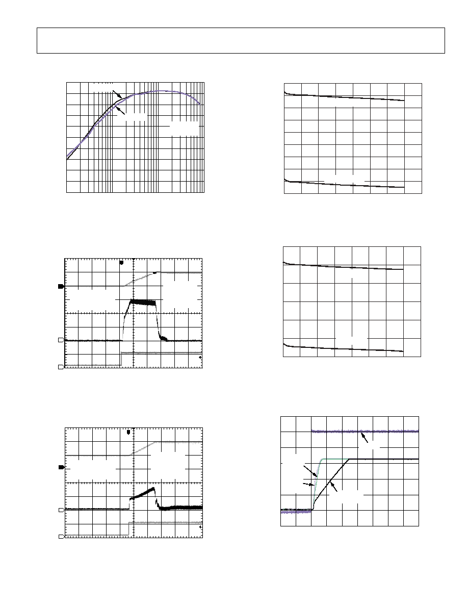
TYPICAL PERFORMANCE CHARACTERISTICS
FREQ = GND
FREQ = VIN
VIN = 5V
V
OUT
= 10V
100
90
80
70
60
50
40
30
20
10
0
1
10
100
1k
I
LOAD
(mA)
05110-049
2.90
2.85
2.80
2.75
2.70
2.65
2.60
2.55
2.50
2.45
OUTPUT VOLTAGE (V)
0
50
100
150
200
250
300
350
400
LOAD CURRENT (mA)
ADJ = OPEN
ADJ = LDO_OUT
05110-050
Figure 3. Efficiency vs. Load Current (mA)
Figure 6. LDO Output Voltage vs. Load Current, VIN = 3.3 V
3.4
3.3
3.2
3.1
3.0
2.9
2.8
OUTPUT VOLTAGE (V)
0
50
100
150
200
250
300
350
400
LOAD CURRENT (mA)
ADJ = GND
ADJ = OPEN
05110-051
1
3
2
T
05110-026
CH1 = V
OUT
5V/DIV
CH2 = IL 1A/DIV
CH3 = SD 5V/DIV
V
IN
= 5V
V
OUT
= 10V
I
OUT
= 200mA
C
SS
= 0F
Figure 7. LDO Output Voltage vs. Load Current, VIN = 5 V
Figure 4. Start-Up Response from Shutdown, C
SS
= 0 F
6
5
4
3
2
1
0
≠1
VOLTS (V)
≠80
≠40
0
40
80
120
160
200
240
TIME (
s)
05110-052
280
SD PIN
750nF
OUTPUT
CAP
10
F OUTPUT
CAP
2.2
F
OUTPUT
CAP
1
3
2
T
05110-027
CH1 = V
OUT
5V/DIV
CH2 = IL 1A/DIV
CH3 = SD 5V/DIV
V
IN
= 5V
V
OUT
= 10V
I
OUT
= 200mA
C
SS
= 10nF
Figure 8. LDO Power-Up Response from Shutdown
Figure 5. Start-Up Response from Shutdown, C
SS
= 10 F

ADD8754
Rev. 0 | Page 10 of 28
6
5
4
3
2
1
0
≠1
VOLTS (V)
≠80
≠40
0
40
80
120
160
200
240
TIME (
s)
05110-053
280
SD PIN
750nF
OUTPUT
CAP
2.2
F OUTPUT
CAP
10
F OUTPUT
CAP
05110-056
3.32
3.30
3.28
3.26
400
200
0
V
OUT
(V)
I
LOAD
(mA)
ADJ = GND
V
OUT
= 20mV/DIV
I
OUT
= 200mA/DIV
T
LOAD STEP FROM 30k
TO 10
Figure 9. LDO Power-Up Response from Shutdown
= 3.3 V
Figure 12. LDO Load Transient Response, V
OUT
6
5
4
3
2
1
0
≠1
VOLTS (V)
≠80
≠40
0
40
80
120
160
200
240
TIME (
s)
05110-054
280
750nF
OUTPUT
CAP
2.2
F OUTPUT
CAP
10
F OUTPUT
CAP
SD PIN
T
05110-057
4V
3V
2V
1V
V
OUT
(V)
V
IN
(V)
ADJ = GND
V
IN HIGH
= 5.5V
V
IN LOW
= 3.8V
Figure 10. LDO Power-Up Response from Shutdown
= 3.3 V
Figure 13. LDO Line Transient Response, V
OUT
05110-055
2.52
2.50
2.48
2.46
300
200
100
0
100
s
ADJ = LDO_OUT
V
OUT
= 20mV/DIV
I
OUT
= 100mA/DIV
V
OUT
(V)
I
LOAD
(mA)
T
05110-058
4V
3V
2.5V
2V
1V
V
OUT
(V)
V
IN
(V)
ADJ = LDO_OUT
V
IN HIGH
= 5.5V
V
IN LOW
= 3.8V
= 2.5 V
Figure 11. LDO Load Transient Response, V
= 2.5 V
Figure 14. LDO Line Transient Response, V
OUT
OUT

ADD8754
Rev. 0 | Page 11 of 28
50k
25k
10k
5k
0k
5.0
4.5
4.0
3.5
3.0
2.5
2.0
1.5
1.0
0.5
DELAY TIME (
s)
0
100
200
300
400
500
600
700
CAPACITANCE CE (pF)
05110-061
0
T
05110-059
1
Ch1
2.00 V
A Ch1 12.0 V
M 40.0ns
: 8.00V
@: 5.04V
: 102ns
@: ≠83.2ns
Rising Slew Rate, VDD_2 = 14 V
Figure 15. V
Figure 17. GPM Delay Time vs. CE Capacitance
COM
1
T
05110-060
Ch1
2.00 V
A Ch1 5.16 V
M 40.0ns
: 8.08V
@: 9.08V
: 60.8ns
@: 1.88
s
Falling Slew Rate, VDD_2 = 14 V
Figure 16. V
COM
ADD8754
Rev. 0 | Page 12 of 28
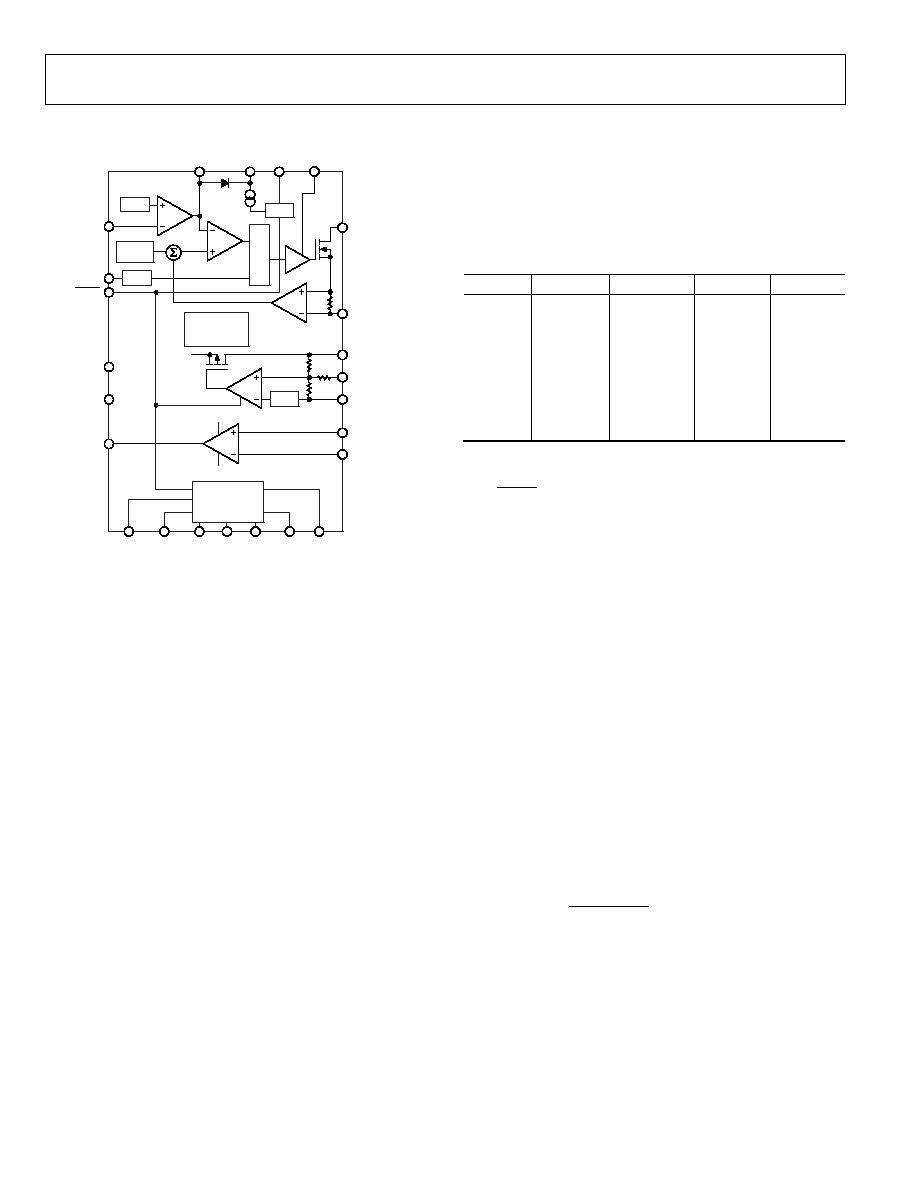
THEORY OF OPERATION
UVLO AND
THERMAL
PROTECTION
VIN_1
REF
GATE HIGH
MOD. CIRCUIT
REF
SLOPE
COMP
OSC
ADD8754
F/F
R
S
Q
BIAS
FB
FREQ
VDD_2
OUT
AGND
SHDN
VGH VGH_M VDD_1 CE
RE
VFLK VDPM
LX
PGND
LDO_OUT
ADJ
POS
NEG
VIN_2
VIN_1
SS
COMP
05110-048
g
m
GND
VDD_2
AGND
V
COM
A 20 nF soft start capacitor results in negligible input-current
overshoot at startup, making it suitable for most applications.
However, if an unusually large output capacitor is used, a longer
soft start period is required to prevent large input inrush current.
Table 8. Typical Soft Start Period
V
Figure 18. Detailed Functional Block Diagram
CURRENT-MODE, STEP-UP SWITCHING
REGULATOR OPERATION
The ADD8754 uses current mode to regulate the output
voltage. This current-mode regulation system allows fast
transient response while maintaining a stable output voltage. By
selecting the proper resistor-capacitor network from COMP to
GND, the regulator response can be optimized for a wide range
of input voltages, output voltages, and load conditions.
Frequency Selection
The ADD8754's frequency is user-selectable to operate either at
650 kHz to optimize the regulator for high efficiency or at
1.2 MHz for small external components. Connect FREQ to
VIN_2 for 1.2 MHz operation, or connect FREQ to GND for
650 kHz operation.
Soft Start Capacitor
The voltage at SS ramps up slowly by charging the soft start
capacitor (C
SS
) with an internal 2.5 A current source. Table 8
lists the values for the soft start period based on maximum
output current and maximum switching frequency.
The soft start capacitor limits the rate of voltage rise on the
COMP pin, which in turn limits the peak switch current at
startup. Table 8 shows a typical soft start period, t
SS
, at the
maximum output current, I
OUT_MAX
, for several conditions.
IN
(V)
V
OUT
(V)
C
OUT
(F)
C
SS
(nF)
t
SS
(ms)
3.3 9
10
20 2.5
3.3 9
10
100 8.2
3.3 12
10
20 3.5
3.3 12
10
100 15
5 9 10 20 0.4
5 9 10 100 1.5
5 12 10 20 0.62
5
12 10 100
2
On/Off Control
The SHDN input turns the ADD8754 on or off. When the step-
up dc-to-dc converter is turned off, there is a dc path from the
input to the output through the inductor and output diode. This
causes the output voltage to remain slightly below the input
voltage by the forward voltage of the diode, preventing the
output voltage from dropping to zero when the regulator is shut
down. See Figure 25 for the typical application circuit to
disconnect the output voltage from the input voltage at
shutdown.
Setting the Output Voltage
The ADD8754 features an adjustable output voltage range of
(V
IN
+ 2 V) to 20 V. The output voltage is set by the resistive
voltage divider from the output voltage (V
OUT
) to the 1.21 V
feedback input at FB. Use the following formula to determine
the output voltage:
= 1.21 V ◊ (1 + R1/R2) (1)
V
OUT
Use an R2 resistance of 10 k or less to prevent output voltage
errors due to the 10 nA FB input bias current. Choose R1 based
on the following formula:
-
V
V
V
OUT
21
.
1
21
.
1
R1 = R2 ◊
For example, R1 = 75.8 k
= 10 V and R2 = 10 k
(2)
with V
OUT

ADD8754
Rev. 0 | Page 13 of 28
Inductor Selection
The inductor ripple current (I
L
) in steady state is
The inductor is an integral part of the step-up converter. It
stores energy during the switch-on time and transfers that
energy to the output through the output diode during the
switch-off time. Use inductance in the range of 1 H to 22 H.
In general, lower inductance values have higher saturation
current and lower series resistance for a given physical size.
However, lower inductance results in higher peak current,
which can lead to reduced efficiency and greater input and/or
output ripple and noise. Peak-to-peak inductor ripple current at
close to 30% of the maximum dc input current typically yields
an optimal compromise.
L
t
V
ON
IN
◊
I =
(5)
L
Solving for the inductance value, L,
L
ON
IN
I
t
V
◊
L
=
(6)
Make sure that the peak inductor current (the maximum input
current plus half of the inductor ripple current) is less than the
rated saturation current of the inductor. In addition, ensure that
the maximum rated rms current of the inductor is greater than
the maximum dc input current to the regulator.
For determining the inductor ripple current, the input (V
IN
) and
output (V
OUT
) voltages determine the switch duty cycle (D) by
the following equation:
D =
OUT
IN
OUT
V
V
V
-
(3)
For duty cycles greater than 50% that occur with input voltages
greater than half the output voltage, slope compensation is
required to maintain stability of the current-mode regulator.
For stable current-mode operation, ensure that the selected
inductance is equal to or greater than L
MIN
:
Using the duty cycle and switching frequency, f
SW
, determine
the on time by using the following equation:
SW
IN
OUT
MIN
f
V
V
L
L
◊
-
=
>
A
8
.
1
(7)
SW
f
D
t
=
(4)
ON
Table 9. Inductor Manufacturers
Vendor
Part
L (H)
Max DC Current
Max DCR (m)
Height (mm)
CMD4D11-2R2MC
2.2
0.95
116
1.2
Sumida
www.sumida.com
CMD4D11-4R7MC
4.7
0.75
216
1.2
CDRH4D28-100
10
1.00
128
3.0
CDRH5D18-220
22
0.80
290
2.0
CR43-4R7 4.7 1.15
109
3.5
CR43-100 10 1.04
182
3.5
DS1608-472 4.7 1.40 60
2.9
Coilcraft
www.coilcraft.com
DS1608-103
10 1.00
75 2.9
D52LC-4R7M 4.7
1.14 87
2.0
Toko
www.tokoam.com
D52LC-100M 10
0.76 150 2.0
ADD8754
Rev. 0 | Page 14 of 28
Choosing the Input and Output Capacitors
Diode Selection
The ADD8754 requires input and output bypass capacitors to
supply transient currents while maintaining a constant input
and output voltage. Use a low effective series resistance (ESR)
10 F or greater input capacitor to prevent noise at the
ADD8754 input. Place the capacitors between VIN_1, VIN_2,
and GND and as close as possible to the ADD8754. Ceramic
capacitors are preferred because of their low ESR character-
istics. Alternatively, use a high value, medium ESR capacitor in
parallel with a 0.1 F low ESR capacitor as close as possible to
the ADD8754.
The output diode conducts the inductor current to the output
capacitor and load while the switch is off. For high efficiency,
minimize the forward voltage drop of the diode. Schottky
diodes are recommended. However, for high voltage, high
temperature applications, where the Schottky diode reverse
leakage current becomes significant and can degrade efficiency,
use an ultrafast junction diode.
The diode must be rated to handle the average output load
current. Many diode manufacturers derate the current
capability of the diode as a function of the duty cycle. Verify
that the output diode is rated to handle the average output load
current with the minimum duty cycle. The minimum duty cycle
of the ADD8754 is
The output capacitor maintains the output voltage and supplies
current to the load while the ADD8754 switch is on. The value
and characteristics of the output capacitor greatly affect the
output voltage ripple and stability of the regulator. Use a low
ESR output capacitor; ceramic dielectric capacitors are
preferred.
OUT
MAX
IN
OUT
MIN
V
V
V
D
_
-
=
(12)
For very low ESR capacitors such as ceramic capacitors, the
ripple current due to the capacitance is calculated as follows.
Because the capacitor discharges during the on time, t
where V
IN_MAX
is the maximum input voltage.
ON
, the
charge removed from the capacitor, Q
C
, is the load current
multiplied by the on time. Therefore, the output voltage ripple
(V
OUT
) is
OUT
ON
L
OUT
C
OUT
C
t
I
C
Q
V
◊
=
=
(8)
where:
C
OUT
is the output capacitance.
I
L
is the average inductor current.
SW
ON
f
D
t
=
(9)
OUT
IN
OUT
V
V
V
D
-
=
(10)
Choose the output capacitor based on the following equation:
OUT
OUT
SW
IN
OUT
L
OUT
V
V
f
V
V
I
C
◊
◊
-
◊
)
(
(11)
Table 10. Capacitor Manufacturers
Vendor Web
Address
AVX
www.avxcorp.com
Murata
www.murata.com
Sanyo
www.sanyovideo.com
Taiyo Yuden
www.t-yuden.com
For example, D
MIN
= 0.45 when V
= 10 V and V
OUT
IN_MAX
= 5.5 V
Table 11. Schottky Diode Manufacturers
Vendor Web
Address
ON Semiconductor
www.onsemi.com
Diodes, Inc.
www.diodes.com
Central Semiconductor Corp. www.centralsemi.com
Sanyo
www.sanyovideo.com
Loop Compensation
Use of external components to compensate the regulator loop
allows optimization of the loop dynamics for a given application.
A step-up converter produces an undesirable right-half plane
zero in the regulation feedback loop. This requires compensat-
ing the regulator such that the crossover frequency occurs well
below the frequency of the right-half plane zero. The right-half
plane zero is determined by the following equation:
L
R
V
V
RHP
F
LOAD
OUT
IN
Z
◊
◊
=
2
)
(
2
(13)
where:
F
Z
(RHP) is the right-half plane zero.
R
LOAD
is the equivalent load resistance, or the output voltage
divided by the load current.
ADD8754
Rev. 0 | Page 15 of 28
To stabilize the regulator, make sure that the regulator crossover
frequency is less than or equal to one-fifth of the right-half
plane zero and less than or equal to one-fifteenth of the
switching frequency.
For V
The regulator loop gain is
OUT
CS
COMP
MEA
OUT
IN
OUT
FB
VL
Z
G
Z
G
V
V
V
V
A
◊
◊
◊
◊
◊
=
(14)
where:
A
VL
is the loop gain.
V
FB
is the feedback regulation voltage, 1.210 V.
V
OUT
is the regulated output voltage.
V
IN
is the input voltage.
G
MEA
is the error amplifier transconductance gain.
Z
COMP
is the impedance of the series RC network from COMP to
GND.
G
CS
is the current sense transconductance gain (the inductor
current divided by the voltage at COMP), which is internally set
by the ADD8754.
Z
OUT
is the impedance of the load and output capacitor.
To determine the crossover frequency, it is important to note
that at that frequency the compensation impedance (Z
COMP
) is
dominated by the resistor and the output impedance (Z
OUT
) is
dominated by the impedance of the output capacitor. Therefore,
when solving for the crossover frequency, (by definition of the
crossover frequency) the equation is simplified to
1
2
1
=
◊
◊
◊
◊
◊
◊
◊
=
OUT
C
CS
C
MEA
OUT
IN
OUT
FB
VL
C
f
G
R
G
V
V
V
V
A
(15)
where:
f
C
is the crossover frequency.
R
C
is the compensation resistor.
Solving for R
C
,
CS
MEA
IN
FB
OUT
OUT
OUT
C
C
G
G
V
V
V
V
C
f
R
◊
◊
◊
◊
◊
◊
◊
=
2
(16)
FB
= 1.21 V, G
MEA
= 100 s, and G = 2 sec,
CS
IN
OUT
OUT
OUT
C
C
V
V
V
C
f
R
◊
◊
◊
◊
◊
=
4
10
55
.
2
(17)
Once the compensation resistor is known, set the zero formed
by the compensation capacitor and resistor to one-fourth of the
crossover frequency, or
C
C
C
R
f
C
◊
◊
=
2
(18)
where C
C
is the compensation capacitor.
REF
FB
C2
C
C
R
C
ERROR AMP
05110-007
G
MEA
Figure 19. Compensation Components
The capacitor C2 is chosen to cancel the zero introduced by
output capacitance ESR.
Solving for C2,
C
OUT
R
C
ESR
C2
◊
=
(19)
For low ESR output capacitance, such as with a ceramic capaci-
tor, C2 is optional. For optimal transient performance, the R
C
and C
C
might need to be adjusted by observing the load
transient response of the ADD8754. For most applications, the
compensation resistor should be in the range of 30 k to
400 k, and the compensation capacitor should be in the range
of 100 pF to 1.2 nF. Table 12 shows external component values
for several applications.
Table 12. Recommended External Components for Various Input/Output Voltage Conditions
V
IN
(V)
V
OUT
(V)
f
SW
L (H)
C
OUT
(F)
C
IN
(F)
R
1
(k)
R
2
(k)
R
C
(k)
C
c
(pF)
I
OUT_MAX
(mA)
5 9 650
kHz
10 10 10 63.4
10 84.5 390 450
5 9 1.2
MHz
4.7 10 10 63.4
10 178 100 450
5 12 650
kHz
10 10 10 88.7
10 140 220 350
5
12 1.2
MHz
4.7 10 10 88.7
10 300 100 350
3.3
9 650
kHz
10 10 10 63.4
10 71.5 820 350
3.3
9 1.2
MHz
4.7 10 10 63.4
10 150 180 350
3.3
12 650
kHz
10 10 10 88.7
10 130 420 250
3.3
12 1.2
MHz
4.7 10 10 88.7
10 280 100 250
ADD8754
Rev. 0 | Page 16 of 28
V
COM
AMPLIFIER
The delay capacitance in farad is calculated using the following
equation:
The output of the V
COM
amplifier is designed to control the
voltage on the V
COM
plane of the LCD display. The V
COM
amplifier is designed to source and sink the capacitive pulse
current and ensure stable operation with high load capacitance.
CE = (Delay Time) ◊ 0.000238
The RE in ohms is calculated using the following equation:
Input Overvoltage Protection
(
)
5000
302
-
◊
=
e
Capacitanc
Load
Rate
Slew
RE
Whenever the input exceeds the supply voltage, attention must
be paid to the input overvoltage characteristics. When an
overvoltage occurs, the amplifier can be damaged, depending
on the voltage level and the magnitude of the fault current.
When the input voltage exceeds the supply voltage by more
than 0.6 V, the internal pin junctions allow current to flow from
the input to the supplies. This input current is not inherently
damaging to the device, provided it is 5 mA or less.
When the voltage on the VDPM pin is less than the turn-on
threshold value, the CE pin is internally connected to GND to
discharge the delay capacitor.
S1
S2
S3
REF
L
O
G
I
C
GND
S4
VIN_1
GATE HIGH
MOD. CIRCUIT
GND
GND
RAMP
RESISTOR
DELAY
CAPACITOR
CE
RE
V
OUT
/VGH
VDD_1
VGH_M
VGH
VDPM
VFLK
CL
05110-008
Short-Circuit Output Conditions
The V
COM
amplifier does not have internal short-circuit protection
circuitry. As a precaution, do not short the output directly to the
positive power supply or to the ground.
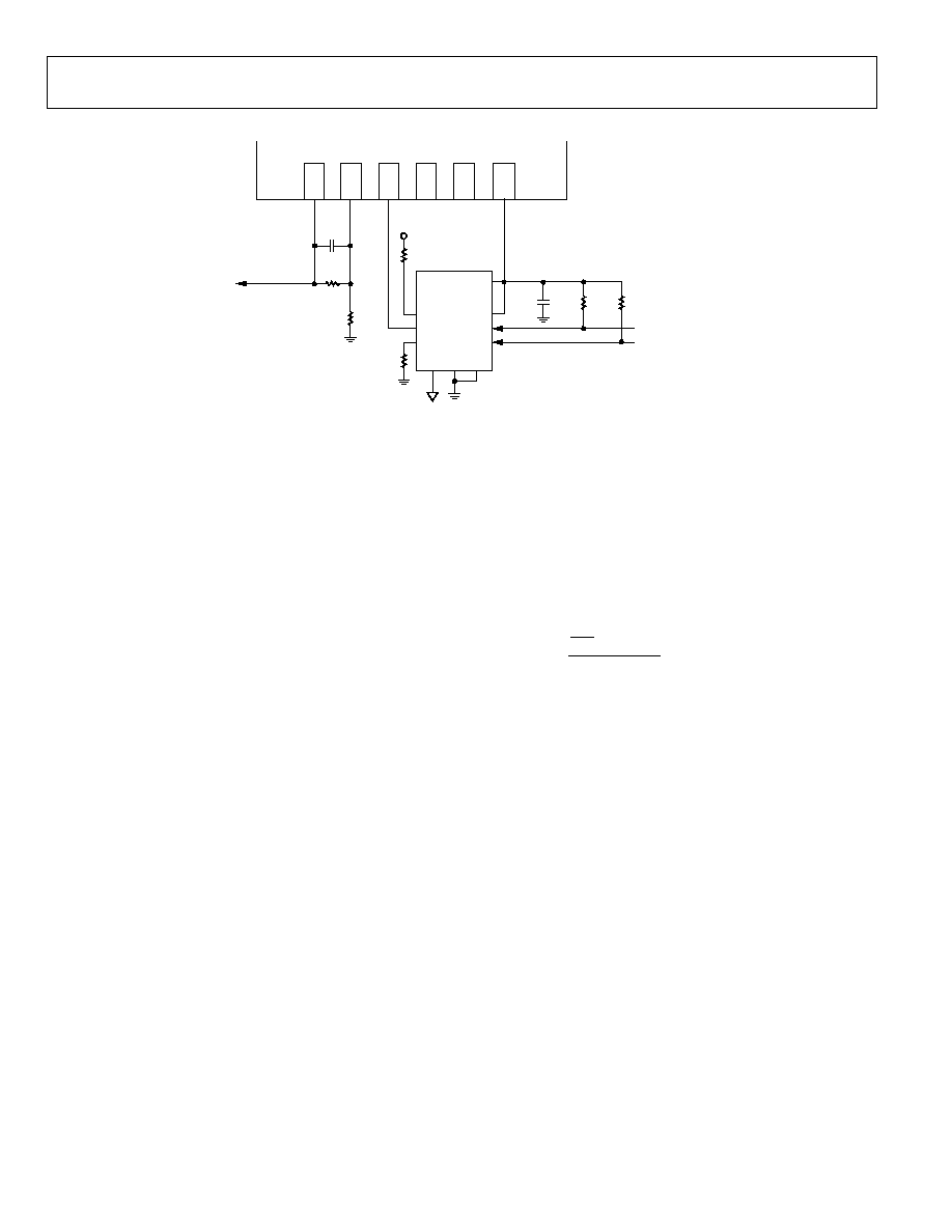
GATE PULSE MODULATOR CIRCUIT
The gate pulse modulator is used for LCD applications in which
shaping of the gate high voltage signal improves image quality.
A charge pump is used to generate the on voltage, VGH. A lower
gate voltage level, VDD_1, is desired during the last portion of
the gate's on time and is provided by VOUT. The integrated gate
pulse modulator circuit provides control over the slope and delay
of the transition between these two TFT on-voltage levels.
Figure 20. Gate Pulse Modulator Functional Block Diagram
The gate pulse modulator circuit has four input pins (VGH,
VDD_1, VDPM, and VFLK) and one output pin (VGH_M).
VFLK is a digital control signal, usually provided by the timing
controller, whose high or low level determines which of the two
input voltages, VGH or VDD_1, is passed through to VGH_M.
The gate high modulator circuit becomes active when the voltage
on pin VDPM exceeds the turn-on threshold value of 2.2 V.
ENABLE ≠ VDPM
CONTROL SIGNAL ≠ VFLK
OUTPUT SIGNAL ≠ VGH_M
WITH LOAD
CAPACITANCE CL
LOW
LOW
LOW
T1
T2
T1
T2
DELAY CONTROLLED
BY CE
VGH
VDD_1
SLOPE CONTROLLED BY RE
05110-009
When the control voltage VFLK switches from logic low to logic
high during normal operation with VDPM at logic high (see
Figure 21), the output voltage VGH_M transitions from VDD_1
to VGH. When the control voltage VFK switches from logic
high to logic low, the output voltage VGH_M transitions from
VGH to VDD_1 after a time delay determined by the size of a
capacitor from the CE pin to the GND and a slew rate
determined by the size of resistor from the RE pin to the GND.
Figure 21. Gate Pulse Modulator Timing Diagram
ADD8754
Rev. 0 | Page 17 of 28
LDO Input Capacitor Selection
POWER-UP SEQUENCE
For the input voltage of the ADD8754 LDO regulator (VIN_1),
a local bypass capacitor is recommended. The input capacitor
provides bypassing for the internal amplifier used in the voltage
regulation loop. Use at least a 1 F low ESR capacitor. Larger
input capacitance and lower ESR provide better supply noise
rejection. Multilayer ceramic chip (MLCC) capacitors provide
the best combination of low ESR and small size.
Most LCD panels require that when VIN is applied, LDO_OUT,
VGL, BOOST_OUT, VGH, and VGH_M are established
sequentially, as indicated in Figure 22. ADD8754 provides this
sequence with appropriate capacitors for the VGL and VGH
charge pumps.
VIN
VDPM
VGH
VGL
BOOST_OUT
LDO_OUT
VGH_M
05110-010
SHDN
SHDN THRESHOLD LEVEL
LDO Output Capacitor Selection
The output capacitor improves the regulator response to sudden
load changes. The output capacitor helps determine the perfor-
mance of any LDO. The ADD8754 LDO requires at least a 2.2 F
capacitor. Transient response is a function of output capacitance,
in that larger values of output capacitance decrease peak devia-
tions, providing improved transient response for large load
current changes.
Choose the capacitors by comparing their lead inductance, ESR,
and dissipation factor. Output capacitance affects stability, and a
larger cap provides a greater phase margin for the ADD8754
LDO. MLCC capacitors provide the best combination of low
ESR and small size.
Figure 22. Power-Up Sequence Timing Diagram
LDO Regulator
Note that the capacitance of some capacitor types show wide
variations over temperature. A good quality dielectric X7R or
better capacitor is recommended.
The ADD8754 low dropout (LDO) regulator has three preset
output voltage settings. As shown in Table 13, by tying the ADJ
pin low, a 3.3 V nominal output is selected. By tying ADJ to the
output voltage, a 2.5 V nominal output is selected. By leaving
ADJ as an open circuit, a nominal voltage of 2.85 V is selected.
SHUTDOWN
Applying a TTL high signal to the shutdown pin (tying it to the
VIN_1) turns on all outputs. Pulling SHDN down to 0.4 V or
below (tying it to GND) turns off all outputs. In shutdown
mode, quiescent current is reduced to a typical value of 300 A.
Table 13. LDO Output Voltage Selection
LDO Output Voltage
ADJ Pin
2.5 V
LDO_OUT
UVLO
2.85 V
No connection
An undervoltage lockout (UVLO) circuit is included with a
built in hysteresis. ADD8754 turns on when VIN_1 rises above
2.8 V and shuts down when VIN_1 falls below 2.6 V.
3.3 V
GND

ADD8754
Rev. 0 | Page 18 of 28
POWER DISSIPATION
The ADD8754's maximum power dissipation depends on the
thermal resistance from the IC die to the ambient environment
and the ambient temperature. The thermal resistance depends
on the IC package, PC board copper area, other thermal mass,
and airflow. The ADD8754, with the exposed backside pad
soldered to a 2-layer PC board with nine 12 mil-diameter
thermal vias, can dissipate about 1.5 W into 65∞C still air before
the die exceeds 125∞C. More PC board copper, cooler ambient
air, and more airflow increase the dissipation capability, whereas
less copper or warmer air decreases the IC's dissipation capability.
The major contributors to the power dissipation are the LDO
regulator and the V
COM
amplifier.
Step-Up Converter
The largest portions of power dissipation in the step-up
converter are the internal MOSFET, the inductor, and the output
diode. For a 90% efficiency step-up converter, about 3% to 5% of
the power is lost in the internal MOSFET, about 3% to 4% in the
inductor, and about 1% in the output diode. The rest of the 1%
to 3% is distributed among the input and output capacitors and
the PC board traces. For an input power of about 3 W, the
power lost in the internal MOSFET is about 90 mW to 150 mW.
LDO
The power dissipated in the LDO depends on the output
current, the output voltage, and the supply voltage:
PD
LDO
= (VIN_1 - LDO_OUT) ◊ I
LDO_OUT
V
COM
Amplifier
The power dissipated in the V
COM
amplifier depends on the
output current, the output voltage, and the supply voltage:
PD
SOURCE
= I
OUT
(source) ◊ (VDD_2 - V
OUT
)
PD
SINK
= I
OUT
(sink) ◊ V
OUT
where:
I
OUT
(source) is the output current sourced by the V
COM
amplifier.
I
OUT
(sink) is the output current that the V
COM
amplifier sinks to
AGND.
In a typical case where the supply voltage is 12 V and the output
voltage is 6 V with an output source current of 20 mA, the
power dissipated is 120 mW.
Thermal Overload Protection
Thermal overload protection prevents excessive power dissipation
from overheating the ADD8754. When the junction temperature
exceeds T
J
= 145∞C, a thermal sensor immediately activates the
fault protection, which shuts down the device, allowing the IC
to cool. The device self-starts once the die temperature falls
below T
J
= 105∞C.
Thermal overload protection protects the controller in the event
of fault conditions. For continuous operation, do not exceed the
absolute maximum junction temperature rating of T
J
= 125∞C.

ADD8754
Rev. 0 | Page 19 of 28
LAYOUT GUIDELINES
When designing a high frequency, switching, regulated power
supply, layout is very important. Using a good layout can solve
many problems associated with these types of supplies. Some of
the main problems are loss of regulation at high output current
and/or large input-to-output voltage differentials, excessive
noise on the output and switch waveforms, and instability.
Using the following guidelines can help minimize these
problems.
Make all power (high current) traces as short, direct, and thick
as possible. It is good practice on a standard PCB board to make
the traces an absolute minimum of 15 mil (0.381 mm) per
Ampere. The inductor, output capacitors, and output diode
should be as close to each other as possible. This helps reduce
the EMI radiated by the power traces that is due to the high
switching currents through them. This also reduces lead
inductance and resistance, which in turn reduce noise spikes,
ringing, and resistive losses that produce voltage errors.
The grounds of the IC, input capacitors, output capacitors, and
output diode (if applicable), should be connected close together,
directly to a ground plane. It is also a good idea to have a ground
plane on both sides of the printed circuit board (PCB). This
reduces noise by reducing ground-loop errors and absorbing
more of the EMI radiated by the inductor.
For multilayer boards of more than two layers, a ground plane
can be used to separate the power plane (power traces and
components) and the signal plane (feedback, compensation,
and components) for improved performance. On multilayer
boards, the use of vias is required to connect traces and different
planes. If a trace needs to conduct a significant amount of current
from one plane to the other, it is good practice to use one standard
via per 200 mA of current. Arrange the components so that the
switching current loops curl in the same direction.
Due to the how switching regulators operate, there are two
power states: one state when the switch is on, and one when the
switch is off. During each state, there is a current loop made by
the power components currently conducting. Place the power
components so that the current loop is conducting in the same
direction during each of the two states. This prevents magnetic
field reversal caused by the traces between the two half cycles
and reduces radiated EMI.
Layout Procedure
To achieve high efficiency, good regulation, and stability, a good
PCB layout is required. It is recommended that the reference
board layout be followed as closely as possible because it is
already optimized for high efficiency and low noise.
Use the following general guidelines when designing PCBs:
1.
Keep CIN close to the IN and GND leads of the ADD8754.
2.
Keep the high current path from CIN (through L1) to the
SW and PGND leads as short as possible.
3.
Keep the high current path from CIN (through L1), D1,
and COUT as short as possible.
4.
Keep high current traces as short and wide as possible.
5.
Keep nodes connected to SW away from sensitive traces
such as FB or COMP to prevent coupling of the traces. If
these traces need to be run near each other, place a ground
trace between the two as a shield.
6.
Place the feedback resistors as close as possible to the FB pin
to prevent noise pickup.
7.
Place the compensation components as close as possible to
the COMP pin.
8.
Avoid routing noise-sensitive traces near the high current
traces and components.
9.
Use a thermal pad size that is the same as the dimension of
the exposed pad on the bottom of the package.
Heat Sinking
When using a surface-mount power IC or external power
switches, the PCB can often be used as the heat sink. This is
done by simply using the copper area of the PCB to transfer
heat from the device.

ADD8754
Rev. 0 | Page 20 of 28
TYPICAL APPLICATION CIRCUITS
LX
VIN_2
FREQ
COMP
SS
VIN_1
GND
VGH_M
VFLK
VDPM
VDD_1
VDD_2
OUT
NE
G
POS
AGND
ADJ
LDO_ OUT
VGH
RE
CE
PGN
D
FB
C8
0.1
F
R8
100k
R7
250k
+14V FROM
V
OUT
VFLK
TO GATE
DRIVER
R3
100k
R4
250k
C9
1
F
CLDO
4.7
F
V
LOGIC
+3.3V
D1
1N5818
COUT
20
F
C
SD
10
F
R
SD
180k
L
10
H
VIN
+5V
V
OUT
+14V
CIN
10
F
C
SS
10nF
R
C
180k
C
C
470pF
R9
10
R1
100k
R2
9.5k
CE
390pF
C1
0.1
F
C5
0.1
F
BAV99
D6
D7
C6
0.1
F
R6
300
RE
33k
C10
0.47
F
VZ1
BZX84C5V1
VGL
≠5V
VZ2
BZX84C28
C7
1
F
C3
1
F
C4
0.47
F
C2
0.1
F
D3
D2
D5
D4
BAV99
BAV99
R5
1k
ADD8754
19
20
21
22
23
24
1
2
3
4
5
6
7
8
9
10
11
12
18
17
16
15
14
13
05110-003
VCOM
+4.0V
SH
D
N
+14V FROM
V
OUT
+14V FROM
V
OUT
Figure 23. 1.2 MHz Application Circuit for TFT LCD Panel with Charge Pumps for VGH and VGL
ADD8754
Rev. 0 | Page 21 of 28
LX
VIN_2
FREQ
COMP
SS
VIN_1
GND
VGH_M
VFLK
VDPM
VDD_1
VDD_2
OUT
NE
G
POS
AGND
ADJ
LDO_ OUT
VGH
RE
CE
PGN
D
FB
C8
0.1
F
R8
100k
R7
250k
VFLK
TO GATE
DRIVER
R3
4.7k
R4
7.5k
C9
1
F
+12V FROM
V
OUT
+12V FROM
V
OUT
CLDO
4.7
F
V
LOGIC
+3.3V
CVGL
0.1
F
VIN
+5V
V
OUT
+12V
CIN
10
F
C
SS
10nF
R
C
180k
C
C
470pF
R1
91k
R2
10k
CE
390pF
D2
1N914
RE
33k
CVGH
10
F
ADD8754
19
20
21
22
23
24
1
2
3
4
5
6
7
8
9
10
11
12
18
17
16
15
14
13
05110-004
VCOM
+4.0V
COUT
20
F
VGL
≠5V
D1
1N5818
+30V
VGH
T
S
HDN
R12
1k
+12V FROM
V
OUT
RVGL
50
VZ1
BZX84C5V1
RVGH
75
VZ2
1N7451A
D3
1N914
T = TRANSTEK MAGNETICS
TMS60059CS
Figure 24. 1.2 MHz Application Circuit for TFT LCD Display with Transformer for VGH and VGL
ADD8754
Rev. 0 | Page 22 of 28
LX
VIN_2
FREQ
COMP
SS
VIN_1
GND
VGH_M
VFLK
VDPM
VDD_1
VDD_2
OUT
NE
G
POS
AGND
ADJ
LDO_ OUT
VGH
RE
CE
PGN
D
FB
C8
0.1
F
R8
100k
R7
250k
+14V FROM
V
OUT
VFLK
TO GATE
DRIVER
R3
100k
R4
250k
C9
1
F
CLDO
4.7
F
V
LOGIC
+3.3V
D1
1N5818
COUT
20
F
L
10
H
VIN
+5V
V
OUT
+14V
CIN
10
F
C
SS
10nF
R
C
180k
C
C
470pF
R9
10
R1
100k
R2
9.5k
CE
390pF
C1
0.01
F
C5
0.01
F
BAV99
D6
D7
C6
0.1
F
R6
300
RE
33k
C10
0.47
F
VZ1
BZX84C5V1
VGL
≠5V
VZ2
BZX84C28
VGH
+28V
C7
1
F
C3
1
F
C4
0.47
F
C2
0.01
F
D3
D2
D5
D4
BAV99
BAV99
R5
1k
ADD8754
19
20
21
22
23
24
1
2
3
4
5
6
7
8
9
10
11
12
18
17
16
15
14
13
05110-005
VCOM
+4.0V
ENABLE
FDC6331
R10
10k
SH
D
N
+14V FROM
V
OUT
+14V FROM
V
OUT
R
SD
180k
C
SD
10
F
Figure 25. 1.2 MHz Application Circuit for TFT LCD Display with Charge Pumps with Input Power Disconnect Switch

ADD8754
Rev. 0 | Page 23 of 28
LX
VIN_2
FREQ
COMP
SS
VIN_1
GND
VGH_M
VFLK
VDPM
VDD_1
VDD_2
OUT
NE
G
POS
AGND
ADJ
LDO_ OUT
VGH
RE
CE
PGN
D
FB
C8
0.1
F
R8
100k
R7
250k
+14V FROM
V
OUT
VFLK
TO GATE
DRIVER
R3
100k
R4
250k
C9
1
F
CLDO
4.7
F
V
LOGIC
+3.3V
D1
1N5818
COUT
20
F
L
10
H
VIN
+5V
V
OUT
+14V
CIN
10
F
C
SS
10nF
R
C
180k
C
C
470pF
R9
10
R1
100k
R2
9.5k
CE
390pF
C1
0.01
F
C5
0.01
F
BAV99
D6
D7
C6
0.1
F
R6
300
RE
33k
C10
0.47
F
VZ1
BZX84C5V1
VGL
≠5V
VZ2
BZX84C28
VGH
+28V
C7
1
F
C3
1
F
C4
0.47
F
C2
0.01
F
D3
D2
D5
D4
BAV99
BAV99
R5
1k
ADD8754
19
20
21
22
23
24
1
2
3
4
5
6
7
8
9
10
11
12
18
17
16
15
14
13
05110-047
VCOM
+4.0V
R10
10k
SH
D
N
+14V FROM
V
OUT
+14V FROM
V
OUT
Q1
2N7000
BOOST AND
CHARGE PUMP
ENABLE
Figure 26. 1.2 MHz Application Circuit for TFT LCD Display with LDO_ALWAYS_ ON
ADD8754
Rev. 0 | Page 24 of 28
OU
T
NE
G
POS
AG
ND
ADJ
LDO
_
OU
T
R
B
6k
C10
2.2pF
ADD8754
05110-006
VCOM
4.0V
R
A
1k
AD5259BRMZ10
VDD
VLOGIC
SCL
SDA
A
W
B
GND AD0 AD1
R4
315k
V
OUT
14V
R3
10k
C9
0.1
F
R10
2.2k
R11
2.2k
SIGNAL FROM FACTORY PC,
SOFTWARE PROVIDED BY ADI
ADJUSTABLE FROM 3V TO 5V WITH
15mV PER STEP ADJUSTMENT
Figure 27. ADD8754 with Programmable V
COM
The V
COM
calibration for flicker reduction is one of the essential
steps in the panel manufacturing process. In a typical panel
production environment, such a process can take additional
time to complete and, therefore, impacts production throughput.
One additional concern is that a potentiometer typically used
only for calibration offers limited resolution. The resistance can
drift over time and can be noticeable after a few years of operation.
The production throughput, image quality, and panel reliability
concerns can all be solved by using a digital potentiometer. As
shown in Figure 27, AD5259, a low cost 256-step digital poten-
tiometer with nonvolatile memory, can calibrate the ADD8754
V
COM
voltage precisely, reliably, and time efficiently.
In the worst case, where the temperature, aging effect, and
resistance tolerance of the AD5259 are all accounted for, the
circuit in Figure 27 makes the V
COM
voltage adjustable from
3.0 V to 5.0 V with 15 mV per step adjustment. A micro-
controller or I
2
C programmer can be used to provide the
control signal for the AD5259, but ADI provides programming
software that simplifies the calibration process. The software
can be installed in the factory computer, and two tester probes
can be connected to the computer's parallel port to implement the
V
COM
programming.
The V
COM
voltage can be calculated as
OUT
AB
AB
COM
V
R
R
R
R
R
D
V
◊
◊
+
+
+
◊
=
7
256
3
4
3
where:
D is the decimal code of the AD5259 programmable resistance
between the W-to-B terminals.
R
AB
is the AD5259 nominal resistance.

ADD8754
Rev. 0 | Page 25 of 28
OUTLINE DIMENSIONS
1
24
6
7
13
19
18
12
2.25
2.10 SQ
1.95
0.60 MAX
0.50
0.40
0.30
0.30
0.23
0.18
2.50 REF
0.50
BSC
12∞ MAX
0.80 MAX
0.65 TYP
0.05 MAX
0.02 NOM
1.00
0.85
0.80
SEATING
PLANE
PIN 1
INDICATOR
TOP
VIEW
3.75
BSC SQ
4.00
BSC SQ
PIN 1
INDICATOR
0.60 MAX
COPLANARITY
0.08
0.20 REF
0.25 MIN
EXPOSED
PAD
(BOTTOM VIEW)
COMPLIANT TO JEDEC STANDARDS MO-220-VGGD-2
Figure 28. 24-Lead Lead Frame Chip Scale Package [LFCSP_VQ]
4 ◊ 4 mm Body, Very Thin Quad
(CP-24-1)
Dimensions shown in millimeters
ORDERING GUIDE
Model
Temperature Range
Package Description
Package Option
Quantity
ADD8754ACPZ-Reel
-40∞C to +85∞C
24-Lead LFCSP_VQ
CP-24-1
5,000
1
ADD8754ACPZ-Reel7
-40∞C to +85∞C
24-Lead LFCSP_VQ
CP-24-1
1,500
1
1
Z = Pb-free part.

ADD8754
Rev. 0 | Page 26 of 28
NOTES

ADD8754
Rev. 0 | Page 27 of 28
NOTES

ADD8754
Rev. 0 | Page 28 of 28
NOTES
©2005 Analog Devices, Inc. All rights reserved. Trademarks and
registered trademarks are the property of their respective owners.
D05110≠0≠4/05(0)