 | –≠–ª–µ–∫—Ç—Ä–æ–Ω–Ω—ã–π –∫–æ–º–ø–æ–Ω–µ–Ω—Ç: ADDAC80 | –°–∫–∞—á–∞—Ç—å:  PDF PDF  ZIP ZIP |

REV. B
Information furnished by Analog Devices is believed to be accurate and
reliable. However, no responsibility is assumed by Analog Devices for its
use, nor for any infringements of patents or other rights of third parties that
may result from its use. No license is granted by implication or otherwise
under any patent or patent rights of Analog Devices.
a
ADDAC80/ADDAC85/ADDAC87
One Technology Way, P.O. Box 9106, Norwood, MA 02062-9106, U.S.A.
Tel: 781/329-4700
www.analog.com
Fax: 781/326-8703
© Analog Devices, Inc., 2002
Complete Low Cost
12-Bit D/A Converters
FUNCTIONAL BLOCK DIAGRAM
*NC = CBI VERSIONS
5V ≠ CCD VERSIONS
(MSB) BIT 1
BIT 2
BIT 3
BIT 4
BIT 5
BIT 6
BIT 7
BIT 8
BIT 9
BIT 10
BIT 11
(LSB) BIT 12
V
REF
OUT
GAIN ADJUST
+V
S
COMMON
SUMMING JUNCTION
20V RANGE
10V RANGE
BIPOLAR OFFSET
REF INPUT
V
OUT
≠V
S
NC/+V
L
*
12-BIT
RESISTOR
LADDER
NETWORK
AND
CURRENT
SWITCHES
REF
CONTROL
CIRCUIT
1
2
3
4
5
6
7
8
9
10
11
12
24
23
22
21
20
19
18
17
16
15
14
13
6.3k
5k
5k
ADDAC80
+
≠
*NC = CBI VERSIONS
5V ≠ CCD VERSIONS
(MSB) BIT 1
BIT 2
BIT 3
BIT 4
BIT 5
BIT 6
BIT 7
BIT 8
BIT 9
BIT 10
BIT 11
(LSB) BIT 12
V
REF
OUT
GAIN ADJUST
+V
S
COMMON
SCALING NETWORK
SCALING NETWORK
SCALING NETWORK
BIPOLAR OFFSET
REF INPUT
I
OUT
≠V
S
NC/+V
L
*
12-BIT
RESISTOR
LADDER
NETWORK
AND
CURRENT
SWITCHES
REF
CONTROL
CIRCUIT
1
2
3
4
5
6
7
8
9
10
11
12
24
23
22
21
20
19
18
17
16
15
14
13
6.3k
2k
5k
5k
FEATURES
Single Chip Construction
On-Board Output Amplifier
Low Power Dissipation: 300 mW
Monotonicity Guaranteed over Temperature
Guaranteed for Operation with 12 V Supplies
Improved Replacement for Standard DAC80, DAC800
Hl-5680
High Stability, High Current Output
Buried Zener Reference
Laser Trimmed to High Accuracy
1/2 LSB Max Nonlinearity
Low Cost Plastic Packaging
PRODUCT DESCRIPTION
The ADDAC80 Series is a family of low cost 12-bit digital-to-
analog converters with both a high stability voltage reference
and output amplifier combined on a single monolithic chip.
The ADDAC80 Series is recommended for all low cost 12-bit D/A
converter applications where reliability and cost are of paramount
importance.
Advanced circuit design and precision processing techniques
result in significant performance advantages over conventional
DAC80 devices. Innovative circuit design reduces the total
power consumption to 300 mW, which not only improves reli-
ability, but also improves long term stability.
The ADDAC80 incorporates a fully differential, nonsaturating
precision current switching cell structure which provides greatly
increased immunity to supply voltage variation. This same struc-
ture also reduces nonlinearities due to thermal transients as the
various bits are switched; nearly all critical components operate
at constant power dissipation. High stability, SiCr thin film
resistors are trimmed with a fine resolution laser, resulting in
lower differential nonlinearity errors. A low noise, high stability,
subsurface Zener diode is used to produce a reference voltage
with excellent long term stability, high external current capabil-
ity and temperature drift characteristics which challenge the
best discrete Zener references.
The ADDAC80 Series is available in three performance grades
and three package types. The ADDAC80 is specified for use
over the 0
∞C to 70∞C temperature range and is available in
both plastic and ceramic DIP packages. The ADDAC85 and
ADDAC87 are available in hermetically sealed ceramic packages
and are specified for the ≠25
∞C to +85∞C and ≠55∞C to +125∞C
temperature ranges.
PRODUCT HIGHLIGHTS
1. The ADDAC80 series of D/A converters directly replaces all
other devices of this type with significant increases in performance.
2. Single chip construction and low power consumption pro-
vides the optimum choice for applications where low cost
and high reliability are major considerations.
3. The high speed output amplifier has been designed to settle
within 1/2 LSB for a 10 V full scale transition in 2.0
µs, when
properly compensated.
4. The precision buried Zener reference can supply up to 2.5 mA
for use elsewhere in the application.
5. The low TC binary ladder guarantees that all units are mono-
tonic over the specified temperature range.
6. System performance upgrading is possible without redesign.

REV. B
≠2≠
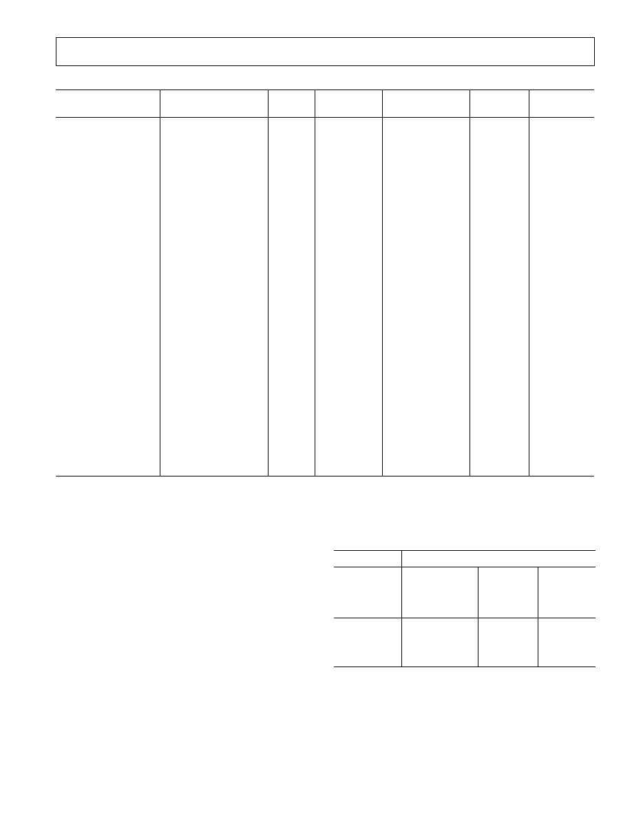
ADDAC80/ADDAC85/ADDAC87≠SPECIFICATIONS
ADDAC80
ADDAC85
ADDAC87
Model
Min
Typ
Max
Min
Typ
Max
Min
Typ
Max
Unit
TECHNOLOGY
Monolithic
Monolithic
Monolithic
DIGITAL INPUT
Binary≠CBI
12
12
12
Bits
BCD≠CCD
Digits
Logic Levels (TTL Compatible)
V
IH
(Logic "1")
2.0
5.5
2.0
5.5
2.0
5.5
V
V
IL
(Logic "0")
0
0.8
0
0.8
0
0.8
V
I
IH
(V
IH
= 5.5 V)
250
250
250
µA
I
IL
(V
IL
= 0.8 V)
100
100
100
µA
TRANSFER CHARACTERISTICS
ACCURACY
Linearity Error @ 25
∞C
CBI
±1/2
±1/2
±1/2
LSB
1
CCD
LSB
T
A
@
T
MIN
to T
MAX
±1/4
±
1/2
±1/4
±
1/2
±1/2
±
3/4
LSB
Differential Linearity Error @ 25
∞C
CBI
±
3/4
±
3/4
±
3/4
LSB
CCD
LSB
T
A
@ T
MIN
to T
MAX
±
3/4
±
1
±
1
LSB
Gain Error
2
±0.1
±
0.3
±0.1
±
0.2
±0.1
±
0.2
%FSR
3
Offset Error
2
±0.05
±
0.15
±0.05
±
0.1
±0.05
±
0.1
%FSR
3
Temperature Range for Guaranteed
Monotonicity
0
+70
≠25
+85
≠55
+125
∞C
DRIFT (T
MIN
to T
MAX
)
Total Bipolar Drift, max (includes gain,
offset, and linearity drifts)
±20
±20
±30
ppm of FSR/
∞C
Total Error (T
MIN
to T
MAX
)
4
Unipolar
±0.08 ±0.15
±0.12 ±0.2
±0.18 ±0.3
% of FSR
Bipolar
±0.06 ±0.10
±0.08 ±0.12
±0.14 ±0.24
% of FSR
Gain Including Internal Reference
±15
±
30
±
20
±
20
ppm of FSR/
∞C
Gain Excluding Internal Reference
±4
±7
±10
±10
ppm of FSR/
∞C
Unipolar Offset
±1
±
3
±
3
±
3
ppm of FSR/
∞C
Bipolar Offset
±5
±
10
±
10
±
10
ppm of FSR/
∞C
CONVERSION SPEED
Voltage Model (V)
5
Settling Time to
±0.01% of FSR for
FSR Change (2 k
500 pF load)
with 10 k
Feedback
3
4
3
4
3
4
µs
with 5 k
Feedback
2
3
2
3
2
3
µs
For LSB Change
1
1
1
µs
Slew Rate
10
10
10
V/
µs
ANALOG OUTPUT
Voltage Models
Ranges≠CBI
±2.5, ±5,
±2.5, ±5,
±2.5, ±5,
V
±10, +5,
±10, +5,
±10, +5,
V
10
10
10
V
≠CCD
V
Output Current
±5
±5
±5
mA
Output Impedance (dc)
0.05
0.05
0.05
Short Circuit Current
40
40
40
mA
Internal Reference Voltage (V
R
)
6.23
6.3
6.37
6.23
6.3
6.37
6.23
6.3
6.37
V
Output Impedance
1.5
1.5
1.5
Max External Current
6
2.5
2.5
2.5
mA
Tempco of Drift
±10
±20
±10
±20
±10
ppm of V
R
/
∞C
POWER SUPPLY SENSITIVITY
±15 V ± 10%, 5 V supply when applicable
0.002
0.002
0.002
% of FSR/%V
S
±12 V ± 5%
0.002
0.002
0.002
% of FSR/%V
S
POWER SUPPLY REQUIREMENTS
Rated Voltages
±15
±15
±15
V
Range
Analog Supplies
±11.4
7
±16.5
±11.4
7
±16.5
±11.4
7
±16.5
V
Logic Supplies
V
Supply Drain
+12 V, +15 V
5
10
5
10
5
10
mA
≠12 V, ≠15 V
14
20
14
20
14
20
mA
(T
A
= 25 C, rated power supplies
unless otherwise noted.)

REV. B
≠3≠
ADDAC80/ADDAC85/ADDAC87
ADDAC80
ADDAC85
ADDAC87
Model
Min
Typ
Max
Min
Typ
Max
Min
Typ
Max
Unit
TEMPERATURE RANGE
Specifications
0
+70
≠25
+85
≠55
+125
∞C
Operating
≠25
+85
≠55
+125
≠55
+125
∞C
Storage
≠25
+125
≠65
+150
≠65
+150
∞C
NOTES
1
Least Significant Bit.
2
Adjustable to zero with external trim potentiometer.
3
FSR means "Full Scale Range" and is 20 V for the
±10 V range and 10 V for the ±5 V range.
4
Gain and offset errors adjusted to zero at 25
∞C.
5
C
F
= 0, see Figure 3a.
6
Maximum with no degradation of specification, must be a constant load.
7
A minimum of
±12.3 V is required for a ±10 V full scale output and ± 11.4 V is required for all other voltage ranges.
Specifications shown in boldface are tested on all production units at final electrical test. Results from those tests are used to calculate outgoing quality levels. All min
and max specifications are guaranteed, although only those shown in boldface are tested on all production units.
Specifications subject to change without notice.
ADDAC80
ADDAC85
ADDAC87
Model
Min
Typ
Max
Min
Typ
Max
Min
Typ
Max
Unit
TECHNOLOGY
Hybrid
Hybrid
Hybrid
DIGITAL INPUT
Binary≠CBI
12
12
12
Bits
BCD≠CCD
3
3
3
Digits
Logic Levels (TTL Compatible)
V
IH
(Logic "1")
2.0
5.5
2.0
5.5
2.0
5.5
V
V
IL
(Logic "0")
0
0.8
0
0.8
0
0.8
V
I
IH
(V
IH
= 5.5 V)
250
250
250
µA
I
IL
(V
IL
= 0.8 V)
≠100
≠100
≠100
µA
TRANSFER CHARACTERISTICS
ACCURACY
Linearity Error @ 25
∞C
CBI
±1/4
±1/2
±1/2
±1/2
LSB
1
CCD
±1/8
±1/4
±1/4
±1/4
LSB
T
A
@
T
MIN
to T
MAX
±1/4
±1/2
±1/4
±1/2
±1/2
±1/2
LSB
Differential Linearity Error @ 25
∞C
CBI
±1/2
±3/4
±1/2
±1/2
LSB
CCD
±1/4
±1/2
±1/2
±1/2
LSB
T
A
@ T
MIN
to T
MAX
±1
±1
±1
LSB
Gain Error
2
±0.1
±0.3
±0.1
±0.1
%FSR
3
Offset Error
2
±0.05 ±0.15
±0.05
±0.05
%FSR
3
Temperature Range for Guaranteed
Monotonicity
0
+70
0
+70
≠25
+85
∞C
DRIFT (T
MIN
to T
MAX
)
Total Bipolar Drift, max (includes gain,
offset, and linearity drifts)
±20
ppm of FSR/
∞C
Total Error (T
MIN
to T
MAX
)
4
Unipolar
±0.08 ±0.15
% of FSR
Bipolar
±0.06 ±0.10
% of FSR
Gain
Including Internal Reference
±15
±30
±20
±20
ppm of FSR/
∞C
Excluding Internal Reference
±5
±7
±10
±10
ppm of FSR/
∞C
Unipolar Offset
±1
±3
±1
±1
ppm of FSR/
∞C
Bipolar Offset
±5
±10
±10
±10
ppm of FSR/
∞C
CONVERSION SPEED
Voltage Model (V)
5
Settling Time to
±0.01% of FSR for
FSR Change (2 k
500 pF load)
with 10 k
Feedback
5
5
5
µs
with 5 k
Feedback
3
3
3
µs
For LSB Change
1.5
1.5
1.5
µs
Slew Rate
10
15
20
20
V/
µs
Current Model (I)
Settling time to
±0.01% of FSR for
FSR Change
10
to 100 Load
300
300
300
ns
for 1 k
1
1
1
µs

REV. B
≠4≠
ADDAC80/ADDAC85/ADDAC87≠SPECIFICATIONS
ADDAC80
ADDAC85
ADDAC87
Model
Min
Typ
Max
Min
Typ
Max
Min
Typ
Max
Unit
ANALOG OUTPUT
Voltage Models
Ranges≠CBI
±2.5, ±5,
±2.5, ±5,
±2.5, ±5,
±10, +5,
±10, +5,
±10, +5,
+10
+10
+10
V
Ranges≠CCD
±10
+10
+10
V
Output Current
±5
±5
±5
mA
Output Impedance (dc)
0.05
0.05
0.05
Short Circuit Duration
Indefinite to Common
Indefinite to Common
Indefinite to Common
Current Models
Ranges≠Unipolar
≠2.0
≠2.0
≠2.0
mA
Ranges≠Bipolar
±1.0
±1.0
±1.0
mA
Output Impedance
Bipolar
3.2
3.2
3.2
k
Unipolar
6.6
6.6
6.6
k
Compliance
≠1.5, +10
≠2.5, +10
≠2.5, +10
V
Internal Reference Voltage (V
R
)
6.17
6.3
6.43
6.17
6.3
6.43
6.17
6.3
6.43
V
Output Impedance
1.5
1.5
1.5
Max External Current
6
2.5
2.5
2.5
mA
Tempco of Drift
±10
±20
±10
±20
±10
±20
ppm of V
R
/
∞C
POWER SUPPLY SENSITIVITY
±15 V ± 10%, 5 V Supply When Applicable
±0.002
±0.002
±0.002
% of FSR/%V
S
POWER SUPPLY REQUIREMENTS
Rated Voltages
±15, +5
±15, +5
±15, +5
V
Range
Analog Supplies
±14
±16
±14.5
±15.5
±14.5
±15.5
V
Logic Supplies
4.5
16
4.5
15.5
4.5
15.5
V
Supply Drain
7
+15 V
10
20
15
20
15
20
mA
≠15 V
20
35
25
30
25
30
mA
+5 V
8
8
20
15
20
15
20
mA
TEMPERATURE RANGE
Specifications
0
+70
0
+70
≠25
+85
∞C
Operating
≠25
+85
≠25
+85
≠55
+125
∞C
Storage
≠55
+130
≠65
+150
≠65
+150
∞C
NOTES
1
Least Significant Bit.
2
Adjustable to zero with external trim potentiometer.
3
FSR means "Full Scale Range" and is 20 V for the
± 10 V range and 10 V for the ± 5 V range.
4
Gain and offset errors adjusted to zero at 25
∞C.
5
C
F
= 0, see Figure 3a.
6
Maximum with no degradation of specification, must be a constant load.
7
Including 5 mA load.
8
5 V supply required only for CCD versions.
Specifications subject to change without notice.
(continued)

REV. B
≠5≠
ADDAC80/ADDAC85/ADDAC87
ADDAC85LD
ADDAC85MIL
ADDAC87
Model
Min
Typ
Max
Min
Typ
Max
Min
Typ
Max
Unit
TECHNOLOGY
Hybrid
Hybrid
Hybrid
DIGITAL INPUT
Binary≠CBI
12
12
12
Bits
BCD≠CCD
Digits
Logic Levels (TTL Compatible)
V
IH
(Logic "1")
2.0
5.5
2.0
5.5
2.0
5.5
V
V
IL
(Logic "0")
0
0.8
0
0.8
0
0.8
V
I
IH
(V
IH
= 5.5 V)
250
250
250
µA
I
IL
(V
IL
= 0.8 V)
≠100
≠100
≠100
µA
TRANSFER CHARACTERISTICS
ACCURACY
Linearity Error @ 25
∞C
CBI
±1/2
±1/2
±1/4
±1/2
LSB
1
CCD
LSB
T
A
@
T
MIN
to T
MAX
±1/2
±3/4
±3/4
LSB
Differential Linearity Error @ 25
∞C
CBI
±1/2
±1/2
±1/2
LSB
CCD
LSB
T
A
@ T
MIN
to T
MAX
±1
±1
±1
LSB
Gain Error
2
±0.1
±0.1
±0.1
±0.2
%FSR
3
Offset Error
2
±0.05
±0.05
±0.05 ±0.1
%FSR
3
Temperature Range for Guaranteed
Monotonicity
≠25
+85
≠55
+125
≠55
+125
∞C
DRIFT (T
MIN
to T
MAX
)
Total Bipolar Drift, max (includes gain,
offset, and linearity drifts)
±15
±30
ppm of FSR/
∞C
Total Error (T
MIN
to T
MAX
)
4
Unipolar
±0.13 ±0.30
% of FSR
Bipolar
±0.12 ±0.24
% of FSR
Gain
Including Internal Reference
±10
±20
±10
±25
ppm of FSR/
∞C
Excluding Internal Reference
±5
±10
ppm of FSR/
∞C
Unipolar Offset
±1
±2
±1
±3
ppm of FSR/
∞C
Bipolar Offset
±5
±10
±5
±10
ppm of FSR/
∞C
CONVERSION SPEED
Voltage Model (V)
5
Settling Time to
±0.01% of FSR
for FSR change (2 k
500 pF load)
with 10 k
Feedback
5
5
5
µs
with 5 k
Feedback
3
3
3
µs
For LSB Change
1.5
1.5
1.5
µs
Slew Rate
20
20
20
V/
µs
Current Model (I)
Settling Time to
±0.01% of FSR
for FSR Change
10
to 100 Load
300
300
300
ns
for 1 k
1
1
1
µs
ANALOG OUTPUT
Voltage Models
Ranges≠CBI
±2.5, ±5,
±2.5, ±5,
±2.5, ±5,
±10, +5,
±10, +5,
±10, +5,
+10
+10
+10
V
Ranges
≠CCD
V
Output Current
±5
±5
±5
mA
Output Impedance (dc)
0.05
0.05
0.05
Short Circuit Duration
Indefinite to Common
Indefinite to Common
Indefinite to Common
Current Models
Ranges≠Unipolar
≠2.0
≠2.0
≠2.0
mA
Ranges
≠Bipolar
±1.0
±1.0
±1.0
mA
Output Impedance
Bipolar
3.2
3.2
2.5
3.2
4.1
k
Unipolar
6.6
6.6
5.0
6.6
8.2
k
Compliance
≠2.5, +10
≠2.5, +10
≠1.5, +10
V
Internal Reference Voltage (V
R
)
6.17
6.3
6.43
6.17
6.3
6.43
6.17
6.3
6.43
V
Output Impedance
1.5
1.5
1.5
Max External Current
6
2.5
2.5
2.5
mA
Tempco of Drift
±10
±20
±10
±20
±5
±10
ppm of V
R
/
∞C
POWER SUPPLY SENSITIVITY
±15 V ± 10%, 5 V supply when applicable
±0.002
±0.002
±0.002 ±0.003
% of FSR/%V
S

REV. B
≠6≠
ADDAC80/ADDAC85/ADDAC87≠SPECIFICATIONS
ADDAC85LD
ADDAC85MIL
ADDAC87
Model
Min
Typ
Max
Min
Typ
Max
Min
Typ
Max
Unit
POWER SUPPLY REQUIREMENTS
Rated Voltages
±15, 5
±15, 5
±15, 5
V
Range
Analog Supplies
±14.5
±15.5
±14.5
±15.5
±13.5
±16.5
V
Logic Supplies
+4.5
±15.5
+4.5
+15.5
+4.5
±16.5
V
Supply Drain
7
+15 V
15
20
15
20
10
20
mA
≠15 V
25
30
25
30
20
35
mA
+5 V
8
15
20
15
20
10
20
mA
TEMPERATURE RANGE
Specification
≠25
+85
≠55
+125
≠55
+125
∞C
Operating
≠55
+125
≠55
+125
≠55
+125
∞C
Storage
≠55
+125
≠55
+125
≠65
+150
∞C
NOTES
1
Least Significant Bit.
2
Adjustable to zero with external trim potentiometer.
3
FSR means "Full-Scale Range" and is 20 V for the
± 10 V range and 10 V for the ± 5 V range.
4
Gain and offset errors adjusted to zero at 25
∞C.
5
C
F
= 0, see Figure 3a.
6
Maximum with no degradation of specification, must be a constant load.
7
Including 5 mA load.
8
5 V supply required only for CCD versions.
Specifications subject to change without notice.
ABSOLUTE MAXIMUM RATINGS
+V
S
to Power Ground . . . . . . . . . . . . . . . . . . . . 0 V to +18 V
≠V
S
to Power Ground . . . . . . . . . . . . . . . . . . . . 0 V to ≠18 V
Digital Inputs (Pins 1 to 12) to Power Ground . . . . . . . . . . .
. . . . . . . . . . . . . . . . . . . . . . . . . . . . . . . . . . ≠1.0 V to +7 V
Ref In to Reference Ground . . . . . . . . . . . . . . . . . . . . .
±12 V
Bipolar Offset to Reference Ground . . . . . . . . . . . . . .
±12 V
10 V Span R to Reference Ground . . . . . . . . . . . . . . .
±12 V
20 V Span R to Reference Ground . . . . . . . . . . . . . . .
±24 V
Ref Out . . . . . . . . . Indefinite Short to Power Ground or +V
S
*NC = CBI VERSIONS
5V ≠ CCD VERSIONS
(MSB) BIT 1
BIT 2
BIT 3
BIT 4
BIT 5
BIT 6
BIT 7
BIT 8
BIT 9
BIT 10
BIT 11
(LSB) BIT 12
V
REF
OUT
GAIN ADJUST
+V
S
COMMON
SUMMING JUNCTION
20V RANGE
10V RANGE
BIPOLAR OFFSET
REF INPUT
V
OUT
≠V
S
NC/+V
L
*
12-BIT
RESISTOR
LADDER
NETWORK
AND
CURRENT
SWITCHES
REF
CONTROL
CIRCUIT
1
2
3
4
5
6
7
8
9
10
11
12
24
23
22
21
20
19
18
17
16
15
14
13
6.3k
5k
5k
ADDAC80
+
≠
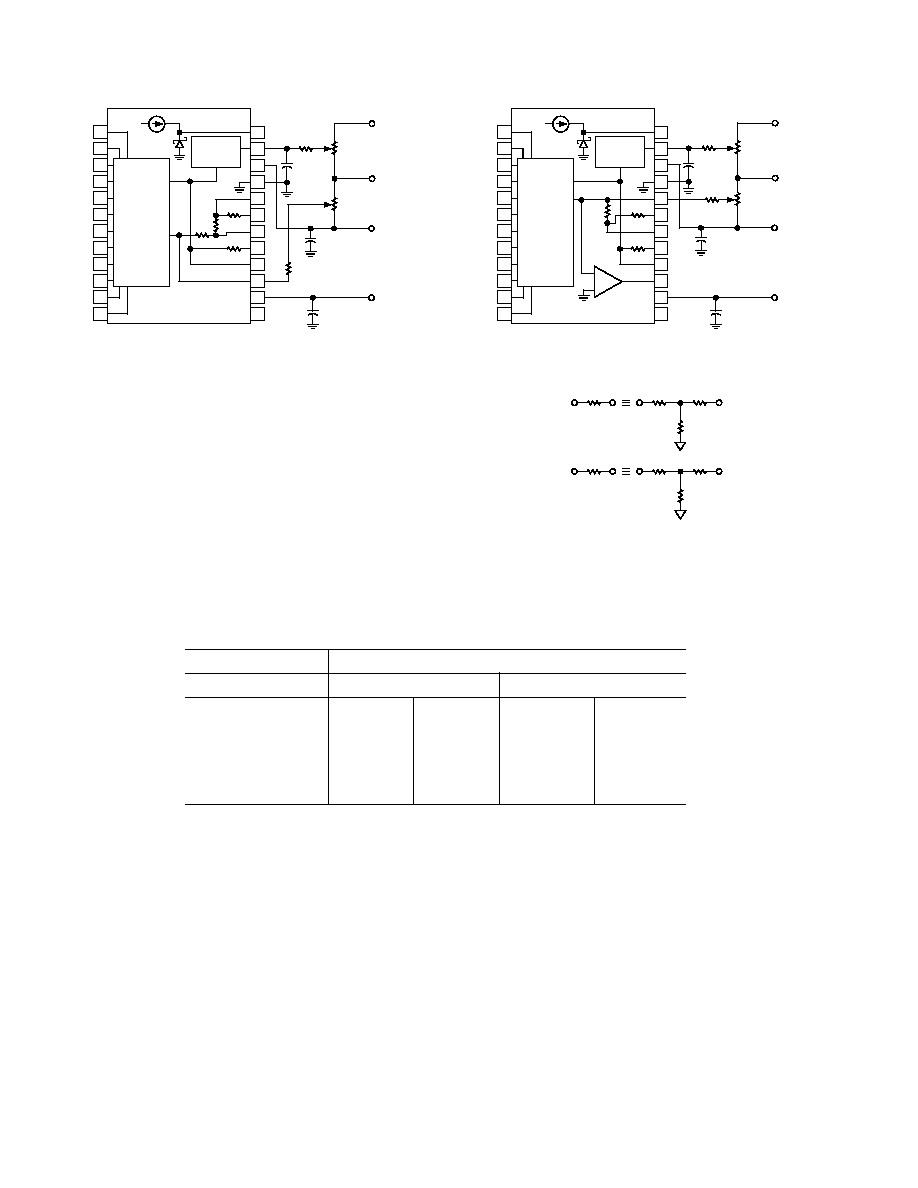
Figure 1. Voltage Model Function Diagram
and Pin Configuration
*NC = CBI VERSIONS
5V ≠ CCD VERSIONS
(MSB) BIT 1
BIT 2
BIT 3
BIT 4
BIT 5
BIT 6
BIT 7
BIT 8
BIT 9
BIT 10
BIT 11
(LSB) BIT 12
V
REF
OUT
GAIN ADJUST
+V
S
COMMON
SCALING NETWORK
SCALING NETWORK
SCALING NETWORK
BIPOLAR OFFSET
REF INPUT
I
OUT
≠V
S
NC/+V
L
*
12-BIT
RESISTOR
LADDER
NETWORK
AND
CURRENT
SWITCHES
REF
CONTROL
CIRCUIT
1
2
3
4
5
6
7
8
9
10
11
12
24
23
22
21
20
19
18
17
16
15
14
13
6.3k
2k
5k
5k
Figure 2. Current Model Functional Diagram
and Pin Configuration
(continued)
REV. B
ADDAC80/ADDAC85/ADDAC87
≠7≠
ORDERING GUIDE
Input
Output
Temperature
Linearity
Package
Model
Code
Mode
Technology
Range
Error
Option
1
ADDAC80N-CBI-V
Binary
Voltage
Monolithic
0
∞C to 70∞C
±1/2 LSB
N-24A
ADDAC80D-CBI-V
Binary
Voltage
Monolithic
0
∞C to 70∞C
±1/2 LSB
D-24
ADDAC85D-CBI-V
Binary
Voltage
Monolithic
≠25
∞C to +85∞C
±1/2 LSB
D-24
ADDAC87D-CBI-V
Binary
Voltage
Monolithic
≠55
∞Cto +125∞C
±1/2 LSB
D-24
ADDAC80-CBI-V
Binary
Voltage
Hybrid
0
∞C to 70∞C
±1/2 LSB
DH-24A
ADDAC80-CBI-I
Binary
Current
Hybrid
0
∞C to 70∞C
±1/2 LSB
DH-24A
ADDAC80-CCD-V
Binary Coded Decimal
Voltage
Hybrid
0
∞C to 70∞C
±1/4 LSB
DH-24A
ADDAC80-CCD-I
Binary Coded Decimal
Current
Hybrid
0
∞C to 70∞C
±1/4 LSB
DH-24A
ADDAC80Z-CBI-V
2
Binary
Voltage
Hybrid
0
∞C to 70∞C
±1/2 LSB
DH-24A
ADDAC80Z-CBI-I
2
Binary
Current
Hybrid
0
∞C to 70∞C
±1/2 LSB
DH-24A
ADDAC80Z-CCD-V
2
Binary Coded Decimal
Voltage
Hybrid
0
∞C to 70∞C
±1/4 LSB
DH-24A
ADDAC80Z-CCD-I
2
Binary Coded Decimal
Current
Hybrid
0
∞C to 70∞C
±1/4 LSB
DH-24A
ADDAC85C-CBI-V
3
Binary
Voltage
Hybrid
0
∞C to 70∞C
±1/2 LSB
DH-24A
ADDAC85C-CBI-I
Binary
Current
Hybrid
0
∞C to 70∞C
±1/2 LSB
DH-24A
ADDAC85-CBI-V
3
Binary
Voltage
Hybrid
≠25
∞C to +85∞C
±1/2 LSB
DH-24A
ADDAC85-CBI-I
3
Binary
Current
Hybrid
≠25
∞C to +85∞C
±1/2 LSB
DH-24A
ADDAC85LD-CBI-V
3
Binary
Voltage
Hybrid
≠25
∞C to +85∞C
±1/2 LSB
DH-24A
ADDAC85LD-CBI-I
3
Binary
Current
Hybrid
≠25
∞C to +85∞C
±1/2 LSB
DH-24A
ADDAC85MIL-CBI-V
3
Binary
Voltage
Hybrid
≠55
∞C to +125∞C
±1/2 LSB
DH-24A
ADDAC85MIL-CBI-I
3
Binary
Current
Hybrid
≠55
∞C to +125∞C
±1/2 LSB
DH-24A
ADDAC85C-CCD-V
3
Binary Coded Decimal
Voltage
Hybrid
0
∞C to 70∞C
±1/4 LSB
DH-24A
ADDAC85C-CCD-I
3
Binary Coded Decimal
Current
Hybrid
0
∞C to 70∞C
±1/4 LSB
DH-24A
ADDAC85-CCD-V
3
Binary Coded Decimal
Voltage
Hybrid
≠25
∞C to +85∞C
±1/4 LSB
DH-24A
ADDAC85-CCD-I
3
Binary Coded Decimal
Current
Hybrid
≠25
∞C to +85∞C
±1/4 LSB
DH-24A
ADDAC85MILCBII8
Binary
Current
Hybrid
≠55
∞C to +125∞C
±1/2 LSB
DH-24A
ADDAC85MILCBIV8
Binary
Voltage
Hybrid
≠55
∞C to +125∞C
±1/2 LSB
DH-24A
ADDAC87-CBI-V
3
Binary
Voltage
Hybrid
≠55
∞C to +125∞C
±1/2 LSB
DH-24A
ADDAC87-CBI-I
3
Binary
Current
Hybrid
≠55
∞C to +125∞C
±1/2 LSB
DH-24A
ADDAC87-CBII883
Binary
Current
Hybrid
≠55
∞C to +125∞C
±1/2 LSB
DH-24A
ADDAC87-CBIV883
Binary
Voltage
Hybrid
≠55
∞C to +125∞C
±1/2 LSB
DH-24A
NOTES
1
For outline information see Package Information section.
2
Z-Suffix devices guarantee performance of 0 V to +5 V and
±5 V spans with minimum supply voltages of ± 11.4 V.
3
These models have been discontinued. This is for historical information only.
PRODUCT OFFERING
Analog Devices has developed a number of technologies to
support products within the data acquisition market. In serving
the market new products are implemented with the technology
best suited to the application. The DAC80 series of products was
first implemented in hybrid form and now it is available in a single
monolithic chip. We will provide both the hybrid and mono-
lithic versions of the family so that in existing designs changes to
documentation or product qualification will not have to be done.
Specifications and ordering information for both versions are
delineated in this data sheet.
DIGITAL INPUT CODES
The ADDAC80 Series accepts complementary digital input
code in binary (CBI) format. The CBI model may be connected
by the user for anyone of three complementary codes: CSB,
COB or CTC.
Table I. Digital Input Codes
Digital Input
Analog Input
CSB
COB
CTC
*
Compl.
Compl.
Compl.
Straight
Offset
Two's
MSB
LSB
Binary
Binary
Compl.
000000000000
+Full-Scale
+Full-Scale
≠1 LSB
011111111111
+1/2 Full-Scale
Zero
≠Full-Scale
100000000000
Midscale
≠1 LSB
+Full-Scale
111111111111
Zero
≠Full-Scale
Zero
*Invert the MSB of the COB code with an external inverter to obtain CTC code.
REV. B
ADDAC80/ADDAC85/ADDAC87
≠8≠
ACCURACY
Accuracy error of a D/A converter is the difference between the
analog output that is expected when a given digital code is
applied and the output that is actually measured with that code
applied to the converter. Accuracy error can be caused by gain
error, zero error, linearity error, or any combination of the three.
Of these three specifications, the linearity error specification is
the most important since it cannot be corrected. Linearity error
is specified over its entire temperature range. This means that
the analog output will not vary by more than its maximum
specification, from an ideal straight line drawn between the
end points (inputs all "1"s and all "0"s) over the specified
temperature range.
Differential linearity error of a D/A converter is the deviation
from an ideal 1 LSB voltage change from one adjacent output
state to the next. A differential linearity error specification of
±1/2 LSB means that the output voltage step sizes can range
from 1/2 LSB to 1 1/2 LSB when the input changes from one
adjacent input state to the next.
DRIFT
Gain Drift
A measure of the change in the full scale range output over
temperature expressed in parts per million of full scale range
per
∞C (ppm of FSR/∞C). Gain drift is established by: 1) testing
the end point differences for each ADDAC80 model at the
lowest operating temperature, 25
∞C and the highest operating
temperature; 2) calculating the gain error with respect to the
25
∞C value and; 3) dividing by the temperature change.
Offset Drift
A measure of the actual change in output with all "1"s on the
input over the specified temperature range. The maximum
change in offset is referenced to the offset at 25
∞C and is
divided by the temperature range. This drift is expressed in
parts per million of full scale range per
∞C (ppm of FSR/∞C).
SETTLING TIME
Settling time for each model is the total time (including slew
time) required for the output to settle within an error band
around its final value after a change in input.
Voltage Output Models
Three settling times are specified to 0.01% of full scale range
(FSR); two for maximum full scale range changes of 20 V, 10 V
and one for a 1 LSB change. The 1 LSB change is measured at
the major carry (0 1 1 1 . . . 1 1 to 1 0 0 0 . . . 0 0), the point at
which the worst case settling time occurs. The settling time
characteristic depends on the compensation capacitor selected,
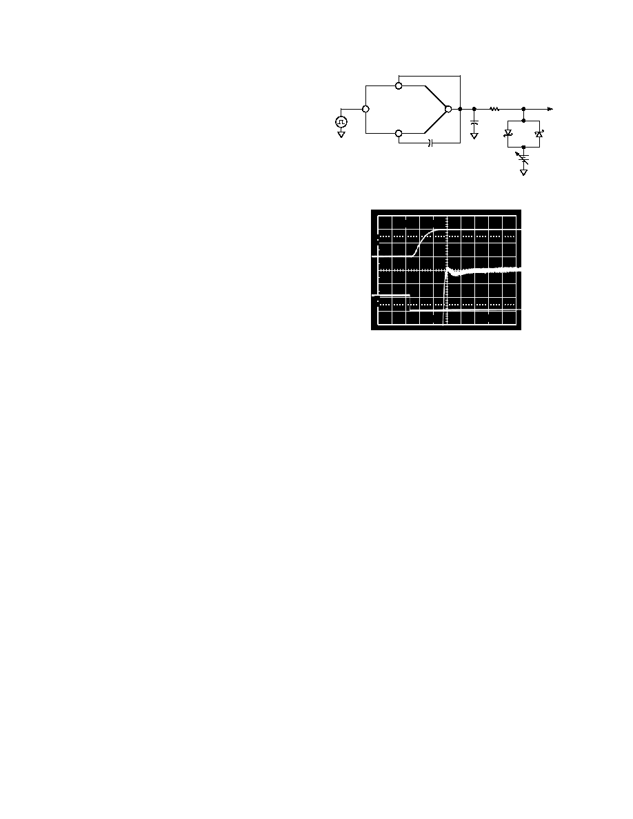
the optimum value is 25 pF as shown in Figure 3a.
Current Output Models
Two settling times are specified to
±0.01% of FSR. Each is given
for current models connected with two different resistive loads:
10
to 100 and 1000 to 1875 . Internal resistors are provided
for connecting nominal load resistances of approximately 1000
to 1800
for output voltage ranges of ±1 V and 0 V to ≠2 V.
10V
V
OUT
DATA
IN
SUMMING
JUNCTION
1≠12
18
20
100pF
2k
10V
HP6216A
TEKTRONIX
7A13
15
C
F
25pF
Figure 3a. Voltage Model Settling Time Circuit
10
0%
100
90
5V
>1mV
500ns
5V
Figure 3b. Voltage Model Settling Time C
F
= 25 pF
POWER SUPPLY SENSITIVITY
Power supply sensitivity is a measure of the effect of a power
supply change on the D/A converter output. It is defined as a
percent of FSR per percent of change in either the positive or
negative supplies about the nominal power supply voltages.
REFERENCE SUPPLY
All models are supplied with an internal 6.3 V reference voltage
supply. This voltage (Pin 24) is accurate to
±1% and must be
connected to the Reference Input (Pin 16) for specified opera-
tion. This reference may also be used externally with external
current drain limited to 2.5 mA. An external buffer amplifier is
recommended if this reference is to be used to drive other sys-
tem components. Otherwise, variations in the load driven by the
reference will result in gain variations. All gain adjustments
should be made under constant load conditions.
ANALYZING DEVICE ACCURACY OVER THE
TEMPERATURE RANGE
For the purposes of temperature drift analysis, the major device
components are shown in Figure 4. The reference element and
buffer amplifier drifts are combined to give the total reference
temperature coefficient. The input reference current to the
DAC, I
REF
, is developed from the internal reference and will
show the same drift rate as the reference voltage. The DAC
output current, I
DAC
, which is a function of the digital input
codes, is designed to track I
REF
; if there is a slight mismatch in
these currents over temperature, it will contribute to the gain
T.C. The bipolar offset resistor, R
BP
, and gain setting resistor,
R
GAIN
, also have temperature coefficients that contribute to
system drift errors. The input offset voltage drift of the output
amplifier, OA, also contributes a small error.

REV. B
ADDAC80/ADDAC85/ADDAC87
≠9≠
15V
+
≠
I
REF
DAC
I
DAC
V≠
+
≠
OA
R
GAIN
R
BP
6.3k
6.3V
Figure 4. Bipolar Configuration
There are three types of drift errors over temperature: offset,
gain, and linearity. Offset drift causes a vertical translation of
the entire transfer curve; gain drift is a change in the slope of the
curve; and linearity drift represents a change in the shape of the
curve. The combination of these three drifts results in the com-
plete specification for total error over temperature.
Total error is defined as the deviation from a true straight line
transfer characteristic from exactly zero at a digital input that
calls for zero output to a point that is defined as full-scale. A
specification for total error over temperature assumes that both
the zero and full-scale points have been trimmed for zero error
at 25
∞C. Total error is normally expressed as a percentage of the
full-scale range. In the bipolar situation, this means the total
range from ≠V
FS
to +V
FS
.
Several new design concepts not previously used in DAC80-type
devices contribute to a reduction in all the error factors over
temperature. The incorporation of low temperature coefficient
silicon-chromium thin-film resistors deposited on a single chip,
a patented, fully differential, emitter weighted, precision current
steering cell structure, and a T.C. trimmed buried Zener diode
reference element results in superior wide temperature range
performance. The gain setting resistors and bipolar offset resis-
tor are also fabricated on the chip with the same SiCr material
as the ladder network, resulting in low gain and offset drift.
MONOTONICITY AND LINEARITY
The initial linearity error of
±1/2 LSB max and the differential
linearity error of
±3/4 LSB max guarantee monotonic performance
over the specified range. It can therefore be assumed that linearity
errors are insignificant in computation of total temperature errors.
UNIPOLAR ERRORS
Temperature error analysis in the unipolar mode is straightforward:
there is an offset drift and a gain drift. The offset drift (which
comes from leakage currents and drift in the output amplifier
(OA)) causes a linear shift in the transfer curve as shown in
Figure 5. The gain drift causes a change in the slope of the
curve and results from reference drift, DAC drift, and drift in
R
GAIN
relative to the DAC resistors.
BIPOLAR RANGE ERRORS
The analysis is slightly more complex in the bipolar mode. In
this mode R
BP
is connected to the summing node of the output
amplifier (see Figure 4) to generate a current that exactly balances
the current of the MSB so that the output voltage is zero with
only the MSB on.
Note that if the DAC and application resistors track perfectly,
the bipolar offset drift will be zero even if the reference drifts. A
change in the reference voltage, which causes a shift in the bipolar
offset, will also cause an equivalent change in I
REF
and thus I
DAC
,
so that I
DAC
will always be exactly balanced by I
BP
with the MSB
turned on. This effect is shown in Figure 5. The net effect of the
reference drift then is simply to cause a rotation in the transfer
around bipolar zero. However, consideration of second order
effects (which are often overlooked) reveals the errors in the
bipolar mode. The unipolar offset drifts previously discussed
will have the same effect on the bipolar offset. A mismatch of R
BP
to the DAC resistors is usually the largest component of bipolar
drift, but in the ADDAC80 this error is held to 10 ppm/
∞C max.
Gain drift in the DAC also contributes to bipolar offset drift,
as well as full-scale drift, but again is held to 10 ppm/
∞C max.
ACTUAL
GAIN SHIFT
IDEAL
OFFSET (ZERO) SHIFT
OUTPUT
UNIPOLAR
INPUT
OUTPUT
OFFSET SHIFT
BIPOLAR (IDEAL CASE)
GAIN SHIFT
INPUT
Figure 5. Unipolar and Bipolar Drifts
USING THE ADDAC80 SERIES
POWER SUPPLY CONNECTIONS
For optimum performance power supply decoupling capacitors
should be added as shown in the connection diagrams. These
capacitors (1
µF electrolytic recommended) should be located
close to the ADDAC80. Electrolytic capacitors, if used, should
be paralleled with 0.01
µF ceramic capacitors for optimum high
frequency performance.
EXTERNAL OFFSET AND GAIN ADJUSTMENT
Offset and gain may be trimmed by installing external OFFSET
and GAIN potentiometers. These potentiometers should be
connected as shown in the block diagrams and adjusted as
described below. TCR of the potentiometers should be 100 ppm/
∞C
or less. The 3.9 M
and 10 M resistors (20% carbon or better)
should be located close to the ADDAC80 to prevent noise pickup.
If it is not convenient to use these high-value resistors, a function-
ally equivalent "T" network, as shown in Figure 8 may be
substituted in each case. The gain adjust (Pin 23) is a high
impedance point and a 0.01
µF ceramic capacitor should be
connected from this pin to common to prevent noise pickup.
REV. B
ADDAC80/ADDAC85/ADDAC87
≠10≠
1 F
3.9M
1 F
0.01 F
10M
+V
S
10k
TO
100k
+V
S
≠V
S
10k
TO
100k
≠V
S
1
2
3
4
5
6
7
8
9
10
11
12
12-BIT
RESISTOR
LADDER
NETWORK
AND
CURRENT
SWITCHES
REF
CONTROL
CIRCUIT
6.3k
2k
3k
5k
24
23
22
21
20
19
18
17
16
15
14
13
Figure 6. External Adjustment and Voltage Supply
Connection Diagram, Current Model
Offset Adjustment
For unipolar (CSB) configurations, apply the digital input code
that should produce zero potential output and adjust the
OFFSET potentiometer for zero output. For bipolar (COB, CTC)
configurations, apply the digital input code that should produce
the maximum negative output voltage. Example: If the FULL
SCALE RANGE is connected for 20 V, the maximum negative
output voltage is ≠10 V. See Table II for corresponding codes.
Gain Adjustment
For either unipolar or bipolar configurations, apply the digital
input that should give the maximum positive voltage output.
Adjust the GAIN potentiometer for this positive full-scale voltage.
See Table II for positive full-scale voltages.
12-BIT
RESISTOR
LADDER
NETWORK
AND
CURRENT
SWITCHES
REF
CONTROL
CIRCUIT
1
2
3
4
5
6
7
8
9
10
11
12
24
23
22
21
20
19
18
17
16
15
14
13
6.3k
5k
5k
+
≠
1 F
1 F
0.01 F
10M
+V
S
10k
TO
100k
+V
S
≠V
S
10k
TO
100k
≠V
S
3.9M
Figure 7. External Adjustment and Voltage Supply
Connection Diagram, Voltage Model
10M
270k
270k
7.8k
3.9M
180k
180k
10k
Figure 8. Equivalent Resistances
Table II. Digital Input Analog Output
Digital Input
Analog Output
12-Bit Resolution
Voltage
*
Current
MSB
LSB
0 to +10 V
10 V
0 to ≠2 mA
1 mA
0 0 0 0 0 0 0 0 0 0 0 0
+9.9976 V
+9.9951 V
≠1.9995 mA
≠0.9995 mA
0 1 1 1 1 1 1 1 1 1 1 1
+5.0000 V
0.0000 V
≠1.0000 mA
0.0000 mA
1 0 0 0 0 0 0 0 0 0 0 0
+4.9976 V
4.88 mV
≠0.9995 mA
+0.0005 mA
1 1 1 1 1 1 1 1 1 1 1 1
0.0000 V
≠10.0000 V
0.0000 mA
≠1.00 mA
l LSB
2.44 mV
≠0.0049 V
0.488
µA
0.488
µA
*To obtain values for other binary ranges 0 to 5 V range: divide 0 to 10 values by 2;
± 5 V range: divide
± 10 V range values by 2; ±2.5 V range: divide ±10 V range values by 4.
REV. B
ADDAC80/ADDAC85/ADDAC87
≠11≠
VOLTAGE OUTPUT MODELS
Internal scaling resistors provided in the ADDAC80 may be
connected to produce bipolar output voltage ranges of
±10 V,
±5 V or ±2.5 V or unipolar output voltage ranges of 0 V to +5 V
or 0 V to +10 V (see Figure 9).
REF
INPUT
TO REF
CONTROL
CIRCUIT
FROM
WEIGHTED
RESISTOR
NETWORK
SUMMING
JUNCTION
6.3k
5k
5k
18
20
16
+
≠
OUTPUT
COM
BIPOLAR
OFFSET
21
15
19
17
Figure 9. Output Amplifier Voltage Range Scaling Circuit
Gain and offset drift are minimized in the ADDAC80 because
of the thermal tracking of the scaling resistors with other device
components. Connections for various output voltage ranges are
shown in Table III. Settling time is specified for a full-scale
range change: 4 s for a 10 k
feedback resistor; 3 s for a 5 k
feedback resistor when using the compensation capacitor shown
in Figure 3a.
The equivalent resistive scaling network and output circuit of
the current model are shown in Figures 10 and 11. External R
LS
resistors are required to produce exactly 0 V to ≠2 V or
± 1 V
output. TCR of these resistors should be
±100 ppm/∞C or less
to maintain the ADDAC80 output specifications. If exact output
ranges are not required, the external resistors are not needed.
17
TO REF CONTROL CIRCUIT
6.3k
3k
2k
19
20
16
18
REF IN
5k
15
Figure 10. Internal Scaling Resistors
6.3k
BIPOLAR OFFSET
REFERENCE
INPUT
I
OUT
COMMON
REFERENCE OUT
6.6k
V
TO REF
CONTROL
CIRCUIT
17
16
I
0 TO 2mA
6.3V
24
21
15
+
≠
Figure 11. ADDAC80 Current Model Equivalent Output Circuit
Internal resistors are provided to scale an external op amp or to
configure a resistive load to offer two output voltage ranges of
±1 V
or 0 V to ≠2 V. These resistors (R
LI
TCR = 20 ppm/
∞C) are an
integral part of the ADDAC80 and maintain gain and bipolar
offset drift specifications. If the internal resistors are not used, exter-
nal R
L
(or R
F
) resistors should have a TCR of
±25 ppm/∞C or
less to minimize drift. This will typically add
±50 ppm/∞C + the
TCR of R
L
(or R
F
) to the total drift.
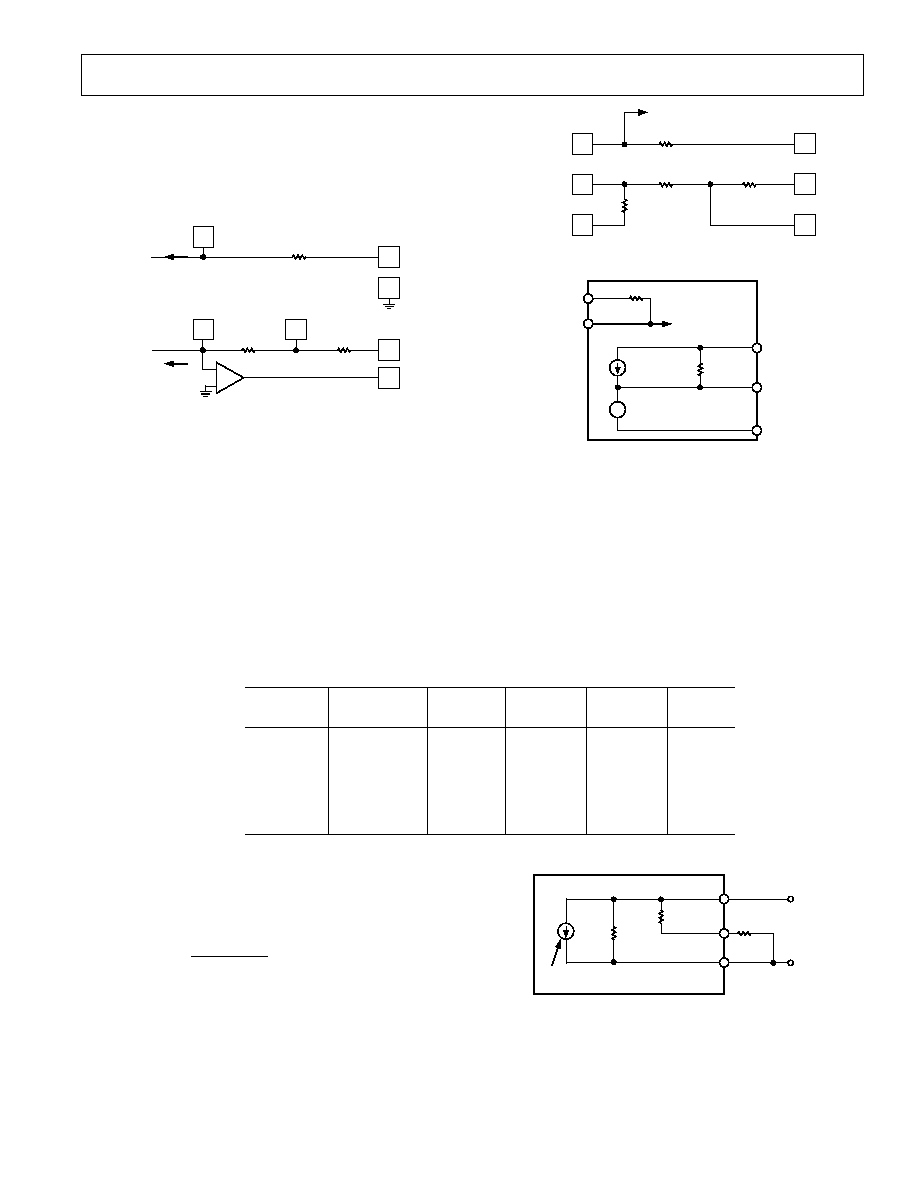
Table III. Output Voltage Range Connections, Voltage Model ADDAC80
Output
Digital
Connect
Connect
Connect
Connect
Range
Input Codes
Pin 15 to
Pin 17 to
Pin 19 to
Pin 16 to
±10 V
COB or CTC
19
20
15
24
±5 V
COB or CTC
18
20
NC
24
±2.5 V
COB or CTC
18
20
20
24
0 V to 10 V
CSB
18
21
NC
24
0 V to 5 V
CSB
18
21
20
24
0 V to 10 V
CCD
19
NC
15
24
NC = No Connect
DRIVING A RESISTIVE LOAD UNIPOLAR
A load resistance, R
L
= R
LI
, + R
LS
, connected as shown in
Figure 12 will generate a voltage range, V
OUT
, determined by:
V
mA
k
R
k
R
OUT
L
L
=
◊
+
≠
.
.
2
6 6
6 6
(1)
where R
L
max = 1.54 k
and V
OUT
max = ≠2.5 V
To achieve specified drift, connect the internal scaling resistor
(R
LI
) as shown in Table IV to an external metal film trim resistor
(R
LS
) to provide full scale output voltage range of 0 V to ≠2 V.
With R
LS
= 0 V, V
OUT
= ≠1.69 V.
0 TO
2mA
CURRENT CONTROLLED
BY DIGITAL INPUT
6.6k
R
LI
968
COMMON
V
OUT
R
LS
+
≠
15
18
21
Figure 12. Equivalent Circuit ADDAC80-CBI-I Connected
for Unipolar Voltage Output with Resistive Load
REV. B
ADDAC80/ADDAC85/ADDAC87
≠12≠
DRIVING A RESISTOR LOAD BIPOLAR
The equivalent output circuit for a bipolar output voltage range
is shown in Figure 13, R
L
= R
LI
+ R
LS
. V
OUT
is determined by:
V
mA
R
k
R
k
OUT
L
L
= ±
◊
+
1
3 22
3 22
.
.
(2)
where R
L
max = 11.18 k
and V
OUT
max =
±2.5 V
To achieve specified drift, connect the internal scaling resistors
(R
LI
) as shown in Table IV for the COB or CTC codes and add
an external metal film resistor (R
LS
) in series to obtain a full scale
output range of
±1 V. In this configuration, with R
LS
equal to
zero, the full scale range will be
±0.874 V.
1mA
CURRENT CONTROLLED
BY DIGITAL INPUT
3.22k
R
LI
1.2k
COMMON
V
OUT
R
LS
+
≠
15
20
21
Figure 13. ADDAC80-CBI-I Connected for Bipolar
Output Voltage with Resistive Load
DRIVING AN EXTERNAL OP AMP
The current model ADDAC80 will drive the summing junction
of an op amp used as a current to voltage converter to produce
an output voltage. As seen in Figure 14,
V
I
R
OUT
OUT
F
=
◊
(3)
where I
OUT
is the ADDAC80 output current and R
F
is the feed-
back resistor. Using the internal feedback resistors of the current
model ADDAC80 provides output voltage ranges the same as
the voltage model ADDAC80. To obtain the desired output
voltage range when connecting an external op amp, refer to
Table V and Figure 14.
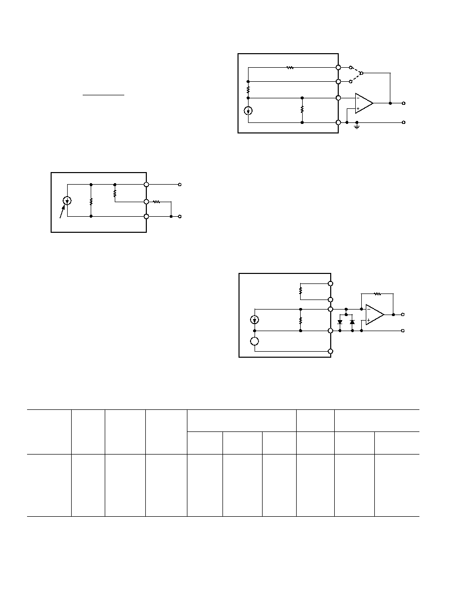
20V RANGE
5k
I
0 TO 2mA
6.6k
5k
CBI
10V RANGE
AD509KH*
V
OUT
*FOR FAST SETTLING TIME
19
18
15
21
A
Figure 14. External Op Amp Using Internal
Feedback Resistors
OUTPUT LARGER THAN 20 V RANGE
For output voltage ranges larger than
±10 V, a high voltage op
amp may be employed with an external feedback resistor. Use
I
OUT
values of
±l mA for bipolar voltage ranges and ≠2 mA for
unipolar voltage ranges (see Figure 15). Use protection diodes
when a high voltage op amp is used.
The feedback resistor, R
F
, should have a temperature coefficient
as low as possible. Using an external feedback resistor, overall
drift of the circuit increases due to the lack of temperature track-
ing between R
F
and the internal scaling resistor network. This will
typically add 50 ppm/
∞C + R
F
drift to total drift.
17
16
15
24
21
V
+
≠
I
0 TO 2mA
V
REF
6.3V
6.6k
6.3k
*FOR OUTPUT VOLTAGE SWINGS UP TO 140V p-p
V
OUT
R
F
171K*
Figure 15. External Op Amp Using External
Feedback Resistors
Table IV. Current Model/Resistive Load Connections
1%
Metal Film
R
LI
Connections
Reference
Bipolar Offset
Internal
External
Digital
Output
Resistance
Resistance
Connect
Connect
Connect
Connect
Connect
Input Codes
Range
R
LI
(k )
R
LS
Pin 15 to
Pin 18 to
Pin 20 to Pin 16 to
Pin 17 to
R
LS
CSB
0 to ≠2 V
0.968
210
20
19 and R
LS
15
24
Com (21)
Between
Pin 18 and
Com (21)
COB or CTC
±1 V
1.2
249
18
19
R
LS
24
15
Between
Pin 20 and
Com (21)
CCD
0 to
±2 V 3
N/A
NC
21
NC
24
NC
N/A

REV. B
ADDAC80/ADDAC85/ADDAC87
≠13≠
OUTLINE DIMENSIONS
Dimensions shown in inches and (mm).
24-Lead Plastic DIP (N-24A)
24
1
12
13
PIN 1
0.580 (14.73)
0.485 (12.32)
1.290 (32.70)
1.150 (29.30)
0.195 (4.95)
0.125 (3.18)
0.015 (0.381)
0.008 (0.204)
0.625 (15.87)
0.600 (15.24)
SEATING
PLANE
0.060 (1.52)
0.015 (0.38)
0.250
(6.35)
MAX
0.022 (0.558)
0.014 (0.356)
0.200 (5.05)
0.125 (3.18)
0.150
(3.81)
MIN
0.100
(2.54)
BSC
0.070 (1.77)
0.030 (0.77)
CONTROLLING DIMENSIONS ARE IN MILLIMETERS: INCH DIMENSIONS
ARE ROUNDED-OFF MILLIMETER EQUIVALENTS FOR REFERENCE
ONLY AND ARE NOT APPROPRIATE FOR USE IN DESIGN
24-Lead Ceramic DIP (D-24)
SEATING
PLANE
0.023 (0.58)
0.014 (0.36)
0.075 (1.91)
0.015 (0.38)
0.225 (5.72)
MAX
0.200 (5.08)
0.120 (3.05)
0.070 (1.78)
0.030 (0.76)
0.150
(3.81)
MIN
1.290 (32.77) MAX
24
1
12
13
0.610 (15.49)
0.500 (12.70)
PIN 1
0.098 (2.49) MAX
0.005 (0.13) MIN
0.620 (15.75)
0.590 (14.99)
0.015 (0.38)
0.008 (0.20)
NOTES
1. INDEX AREA; A NOTCH OR A LEAD ONE IDENTIFICATION MARK IS LOCATED ADJACENT TO LEAD ONE.
2. THE MINIMUM LIMIT FOR DIMENSION MAY BE 0.023" (0.58 mm) FOR ALL FOUR CORNER LEADS ONLY.
3. DIMENSION SHALL BE MEASURED FROM THE SEATING PLANE TO THE BASE PLANE.
4. THIS DIMENSION ALLOWS FOR OFF-CENTER LID, MENISCUS AND GLASS OVERRUN.
5. APPLIES TO ALL FOUR CORNERS.
6. ALL LEADS -- INCREASE MAXIMUM LIMIT BY 0.003" (0.08 mm) MEASURED AT THE CENTER OF THE FLAT,
WHEN HOT SOLDER DIP LEAD FINISH IS APPLIED.
7. TWENTY TWO SPACES.
8. CONTROLLING DIMENSIONS ARE IN MILLIMETERS. INCH DIMENSIONS ARE ROUNDED-OFF MILLIMETER
EQUIVALENTS FOR REFERENCE ONLY AND ARE NOT APPROPRIATE FOR USE IN DESIGN
SEE NOTE 5
SEE NOTE 1
SEE NOTE 7
SEE NOTE 3
SEE NOTE 2, 6
SEE NOTE 4
0.110 (2.79)
0.090 (2.29)
SEE NOTE 4
SEE NOTE 6
Table V. External Op Amp Voltage Mode Connections
Output
Digital
Connect
Connect
Connect
Connect
Range
Input Codes
A to
Pin 17 to
Pin 19 to
Pin 16 to
±10 V
COB or CTC
19
15
A
24
±5 V
COB or CTC
18
15
NC
24
±2.5 V
COB or CTC
18
15
15
24
0 V to 10 V
CSB
18
21
NC
24
0 V to 5 V
CSB
18
21
15
24

REV. B
ADDAC80/ADDAC85/ADDAC87
≠14≠
OUTLINE DIMENSIONS
Dimensions shown in inches and (mm).
24-Lead Side Brazed Ceramic DIP for Hybrid (DH-24A)
SEATING
PLANE
0.023 (0.58)
0.014 (0.36)
0.075 (1.91)
0.015 (0.38)
0.225 (5.72)
MAX
0.200 (5.08)
0.120 (3.05)
0.070 (1.78)
0.030 (0.76)
0.180
(4.57)
MIN
1.212 (29.69) MAX
0.100 (2.54)
BSC
0.098 (2.49) MAX
0.005 (0.13) MIN
0.620 (15.75)
0.590 (14.99)
0.015 (0.38)
0.008 (0.20)
24
12
13
1
PIN 1
NOTES
1. INDEX AREA; A NOTCH OR A LEAD ONE IDENTIFICATION MARK IS LOCATED ADJACENT TO LEAD ONE.
2. THE MINIMUM LIMIT FOR DIMENSION MAY BE 0.023" (0.58 mm) FOR ALL FOUR CORNER LEADS ONLY.
3. DIMENSION SHALL BE MEASURED FROM THE SEATING PLANE TO THE BASE PLANE.
4. THE BASIC PIN SPACING IS 0.100" (2.54 mm) BETWEEN CENTERLINES.
5. APPLIES TO ALL FOUR CORNERS.
6. SHALL BE MEASURED AT THE CENTERLINE OF THE LEADS.
7. TWENTY TWO SPACES.
8. CONTROLLING DIMENSIONS ARE IN MILLIMETERS: INCH DIMENSIONS ARE ROUNDED-OFF MILLIMETER
EQUIVALENTS FOR REFERENCE ONLY AND ARE NOT APPROPRIATE FOR USE IN DESIGN.
SEE NOTE 5
SEE NOTE 1
SEE NOTE 2
SEE NOTE 6
SEE NOTE 3
SEE NOTE 4, 7
0.600 (14.70)
0.580 (14.21)

REV. B
ADDAC80/ADDAC85/ADDAC87
≠15≠
Revision History
Location
Page
Data Sheet changed from REV. A to REV. B.
Update OUTLINE DIMENSION drawings . . . . . . . . . . . . . . . . . . . . . . . . . . . . . . . . . . . . . . . . . . . . . . . . . . . . . . . . . . . . . . . . . . . 1

≠16≠
C00381≠0≠1/02(B)
PRINTED IN U.S.A.