 | ÐлекÑÑоннÑй компоненÑ: ADG1212 | СкаÑаÑÑ:  PDF PDF  ZIP ZIP |
Äîêóìåíòàöèÿ è îïèñàíèÿ www.docs.chipfind.ru
1 pF Off Capacitance, 1 pC Charge Injection,
±15 V/12 V
iCMOSTM Quad SPST Switches
Preliminary Technical Data
ADG1211/ADG1212/ADG1213
Rev. PrE
Information furnished by Analog Devices is believed to be accurate and reliable.
However, no responsibility is assumed by Analog Devices for its use, nor for any
infringements of patents or other rights of third parties that may result from its use.
Specifications subject to change without notice. No license is granted by implication
or otherwise under any patent or patent rights of Analog Devices. Trademarks and
registered trademarks are the property of their respective owners.
One Technology Way, P.O. Box 9106, Norwood, MA 02062-9106, U.S.A.
Tel: 781.329.4700
www.analog.com
Fax: 781.326.8703
© 2004 Analog Devices, Inc. All rights reserved.
FEATURES
2 pF off capacitance
1 pC charge injection
33 V supply range
150 on resistance
Fully specified at +12 V, ±15 V
No V
L
supply required
3 V logic-compatible inputs
Rail-to-rail operation
16-lead TSSOP and 16-lead LFCSP packages
Typical power consumption: <0.03 µW
APPLICATIONS
Automatic test equipment
Data aquisition systems
Battery-powered systems
Sample-and-hold systems
Audio signal routing
Video signal routing
Communication systems
GENERAL DESCRIPTION
The ADG1211/ADG1212/ADG1213 are monolithic CMOS
devices containing four independently selectable switches
designed on an iCMOS process. iCMOS (industrial-CMOS) is a
modular manufacturing process combining high voltage CMOS
(complementary metal-oxide semiconductor) and bipolar
technologies. It enables the development of a wide range of high
performance analog ICs capable of 30 V operation in a footprint
that no previous generation of high voltage parts has been able
to achieve. Unlike analog ICs using conventional CMOS proc-
esses, iCMOS components can tolerate high supply voltages,
while providing increased performance, dramatically lower
power consumption, and reduced package size.
The ultralow capacitance and charge injection of these switches
make them ideal solutions for data acquisition and sample-and-
hold applications, where low glitch and fast settling are required.
Fast switching speed coupled with high signal bandwidth make
the parts suitable for video signal switching.
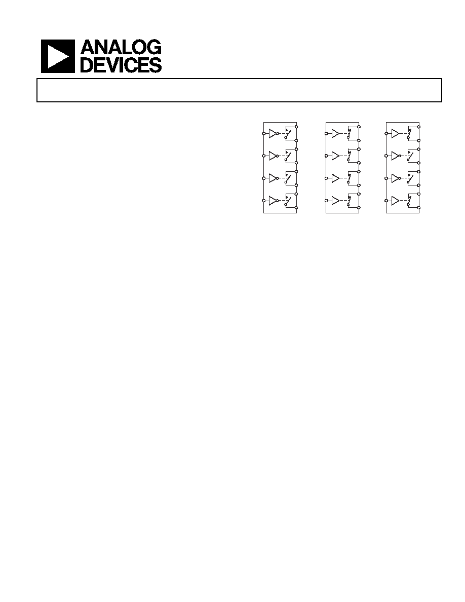
FUNCTIONAL BLOCK DIAGRAM
IN1
IN2
IN3
IN4
S1
D1
S2
D2
S3
D3
S4
D4
ADG1211
SWITCHES SHOWN FOR A LOGIC 1 INPUT
IN1
IN2
IN3
IN4
S1
D1
S2
D2
S3
D3
S4
D4
ADG1212
IN1
IN2
IN3
IN4
S1
D1
S2
D2
S3
D3
S4
D4
ADG1213
04778-
0-
001
Figure 1.
iCMOS construction ensures ultralow power dissipation,
making the parts ideally suited for portable and battery-
powered instruments.
The ADG1211/ADG1212/ADG1213 contain four independent
single-pole/single-throw (SPST) switches. The ADG1211 and
ADG1212 differ only in that the digital control logic is inverted.
The ADG1211 switches are turned on with Logic 0 on the
appropriate control input, while Logic 1 is required for the
ADG1212. The ADG1213 has two switches with digital control
logic similar to that of the ADG1211; the logic is inverted on the
other two switches. Each switch conducts equally well in both
directions when on, and has an input signal range that extends
to the supplies. In the off condition, signal levels up to the
supplies are blocked.
The ADG1213 exhibits break-before-make switching action for
use in multiplexer applications. Inherent in the design is low
charge injection for minimum transients when switching the
digital inputs.
PRODUCT HIGHLIGHTS
1. 2 pF off capacitance (±15 V supply).
2. 1 pC charge injection.
3. 3 V logic-compatible digital inputs: V
IH
= 2.0 V, V
IL
= 0.8 V.
4. No V
L
logic power supply required.
5. Ultralow power dissipation: <0.03 µW.
6. 16-lead TSSOP and 4 mm × 4 mm LFCSP packages.

ADG1211/ADG1212/ADG1213
Preliminary Technical Data
Rev. PrE | Page 2 of 16
TABLE OF CONTENTS
Specifications..................................................................................... 3
Single Supply ................................................................................. 3
Absolute Maximum Ratings............................................................ 6
ESD Caution.................................................................................. 6
Pin Configurations and Function Descriptions ........................... 7
Terminology .......................................................................................8
Typical Performance Characteristics ..............................................9
Test Circuits..................................................................................... 12
Outline Dimensions ....................................................................... 14
Ordering Guide .......................................................................... 14
REVISION HISTORY
11/04--Revision PrE: Preliminary Version

Preliminary Technical Data
ADADG1211/ADG1212/ADG1213
Rev. PrE | Page 3 of 16
SPECIFICATIONS
SINGLE SUPPLY
V
DD
= 15 V ± 10%, V
SS
= -15 V, GND = 0 V, unless otherwise noted.
Table 1.
Parameter
25°C
85°C
Y Version
1
Unit
Test Conditions/Comments
ANALOG
SWITCH
Analog Signal Range
V
DD
to V
SS
V
On Resistance (R
ON
)
120
160
180
typ
V
S
= ±10 V, I
S
= -10 mA; Figure 20
max
On Resistance Match between
Channels (R
ON
)
5
typ
V
S
= ±10 V , I
S
= -10 mA
max
On Resistance Flatness (R
FLAT(ON)
)
25
typ
V
S
= -5 V/0 V/+5 V; I
S
= -10 mA
50
max
LEAKAGE
CURRENTS
V
DD
= +10 V, V
SS
= -10 V
Source Off Leakage, I
S
(Off)
±0.01
nA typ
V
S
= 0 V/10 V, V
D
= 10 V/0 V; Figure 21
±0.5
±1
±5
nA max
Drain Off Leakage, I
D
(Off)
±0.01
nA typ
V
S
= 0 V/10 V, V
D
= 10 V/0 V; Figure 21
±0.5
±1
±5
nA max
Channel On Leakage, I
D
, I
S
(On)
±0.04
nA typ
V
S
= V
D
= 0 V or 10 V; Figure 22
±1
±2
±5
nA max
DIGITAL
INPUTS
Input High Voltage, V
INH
2.0
V min
Input Low Voltage, V
INL
0.8
V max
Input Current, I
INL
or I
INH
0.005
±2.5
µA typ
V
IN
= V
INL
or V
INH
±0.5
µA max
Digital Input Capacitance, C
IN
5
pF typ
DYNAMIC CHARACTERISTICS
2
t
ON
50
ns typ
R
L
= 300 , C
L
= 35 pF
ns max
V
S
= ±10 V; Figure 23
t
OFF
15
ns typ
R
L
= 300 , C
L
= 35 pF
ns max
V
S
= ±10 V; Figure 23
Break-before-Make Time Delay, t
D
15
ns typ
R
L
= 300 , C
L
= 35 pF
1
ns
min
V
S1
= V
S2
= 10 V; Figure 24
Charge Injection
1
pC typ
V
S
= 0 V, R
S
= 0 , C
L
= 1 nF; Figure 25
Off Isolation
75
dB typ
R
L
= 50 , C
L
= 5 pF, f = 1 MHz; Figure 26
Channel-to-Channel Crosstalk
85
dB typ
R
L
= 50 , C
L
= 5 pF, f = 1 MHz; Figure 27
Total Harmonic Distortion + Noise
0.002
% typ
R
L
= 600 , 5 V rms, f = 20 Hz to 20 kHz
-3 dB Bandwidth
700
MHz typ
R
L
= 50 , C
L
= 5 pF; Figure 28
C
S
(Off)
2
pF typ
C
D
(Off)
2
pF typ
C
D
, C
S
(On)
4
pF typ
POWER
REQUIREMENTS
V
DD
= +16.5 V, V
SS
= -16.5 V
I
DD
0.001
µA typ
Digital Inputs = 0 V or V
DD
5.0
µA max
I
DD
0.001
µA typ
Digital Inputs = 5 V
5.0
µA max
I
SS
0.001
µA typ
Digital Inputs = 0 V or V
DD
5.0
µA max

ADG1211/ADG1212/ADG1213
Preliminary Technical Data
Rev. PrE | Page 4 of 16
Parameter
25°C
85°C
Y Version
1
Unit
Test Conditions/Comments
I
GND
0.001
µA typ
Digital Inputs = 0 V or V
DD
5.0
µA max
I
GND
0.001
µA typ
Digital Inputs = 5 V
5.0
µA max
1
Temperature range for Y Version is
-40°C to +125°C.
2
Guaranteed by design, not subject to production test.
V
DD
= 12 V ± 10%, V
SS
= 0 V, GND = 0 V, unless otherwise noted.
Table 2.
Parameter
25°C 85°C Y
Version
1
Unit Test
Conditions/Comments
ANALOG
SWITCH
Analog Signal Range
0 V to V
DD
V
On Resistance (R
ON
)
220 250
typ
V
S
= +10 V, I
S
= -10 mA; Figure 20
max
On Resistance Match between
Channels (R
ON
)
1
typ
V
S
= +10 V, I
S
= -10 mA
max
On -Resistance Flatness (R
FLAT(ON)
)
12
typ
V
S
= -5 V/0 V/+5 V, I
S
= -10 mA
LEAKAGE
CURRENTS
V
DD
= 12 V
Source Off Leakage, I
S
(Off)
±0.01
nA typ
V
S
= 1 V/10 V, V
D
= 10 V/0 V; Figure 21
±0.5
±2.5
nA max
Drain Off Leakage, I
D
(Off)
±0.01
nA typ
V
S
= 1 V/10 V, V
D
= 10 V/0 V; Figure 21
±0.5
±2.5
nA max
Channel On Leakage, I
D
, I
S
(On)
±0.04
nA typ
V
S
= V
D
= 1 V or 10 V; Figure 22
±1
±5
nA max
DIGITAL
INPUTS
Input High Voltage, V
INH
2.0
V min
Input Low Voltage, V
INL
0.8
V max
Input Current, I
INL
or I
INH
0.001
µA typ
V
IN
= V
INL
or V
INH
±0.5
µA max
Digital Input Capacitance, C
IN
5
pF typ
DYNAMIC CHARACTERISTICS
2
t
ON
50
ns
typ
R
L
= 300 , C
L
= 35 pF
ns max
V
S
= 8 V; Figure 23
t
OFF
15
ns typ
R
L
= 300 , C
L
= 35 pF
ns max
V
S
= 8 V; Figure 23
Break-before-Make Time Delay, t
D
15
ns typ
R
L
= 300 , C
L
= 35 pF
1
ns
min
V
S1
= V
S2
= 8 V; Figure 24
Charge Injection
5
pC typ
V
S
= 0 V, R
S
= 0 , C
L
= 1 nF; Figure 25
Off Isolation
75
dB typ
R
L
= 50 , C
L
= 5 pF, f = 1 MHz; Figure 267
Channel-to-Channel Crosstalk
85
dB typ
R
L
= 50 , C
L
= 5 pF, f = 1 MHz; Figure 27
-3 dB Bandwidth
100
MHz typ
R
L
= 50 , C
L
= 5 pF; Figure 28
C
S
(Off)
2
pF typ
C
D
(Off)
2
pF typ
C
D
, C
S
(On)
4
pF typ

Preliminary Technical Data
ADADG1211/ADG1212/ADG1213
Rev. PrE | Page 5 of 16
Parameter
25°C 85°C Y
Version
1
Unit Test
Conditions/Comments
POWER
REQUIREMENTS
V
DD
= 13.2 V
I
DD
0.001
µA typ
Digital Inputs = 0 V or V
DD
5.0
µA max
I
DD
0.001
µA typ
Digital Inputs = 5 V
5.0
µA max
1
Temperature range for Y Version is
-40°C to +125°C.
2
Guaranteed by design, not subject to production test.
ADG1211/ADG1212/ADG1213
Preliminary Technical Data
Rev. PrE | Page 6 of 16
ABSOLUTE MAXIMUM RATINGS
T
A
= 25°C, unless otherwise noted.
Table 3.
Parameter Rating
V
DD
to V
SS
35 V
V
DD
to GND
-0.3 V to +25 V
V
SS
to GND
+0.3 V to -25 V
Analog Inputs
1
V
SS
0.3 V to V
DD
+ 0.3 V
Digital Inputs
1
GND 0.3 V to V
DD
+ 0.3 V or
30 mA, whichever occurs first
Peak Current, S or D
100 mA (pulsed at 1 ms, 10%
duty cycle max)
Continuous Current, S or D
30 mA
Operating Temperature Range
Industrial (B Version)
-40°C to +85°C
Automotive (Y Version)
-40°C to +125°C
Storage Temperature Range
-65°C to +150°C
Junction Temperature
150°C
16-Lead TSSOP,
JA
Thermal
Impedance
150.4°C/W
16-Lead LFCSP,
JA
Thermal
Impedance
30.4°C/W
Lead Temperature, Soldering
Vapor Phase (60 s)
215°C
Infrared (15 s)
220°C
1
Overvoltages at IN, S, or D are clamped by internal diodes. Current should be
limited to the maximum ratings given.
Stresses above those listed under Absolute Maximum Ratings
may cause permanent damage to the device. This is a stress
rating only; functional operation of the device at these or any
other conditions above those listed in the operational sections
of this specification is not implied. Exposure to absolute
maximum rating conditions for extended periods may affect
device reliability. Only one absolute maximum rating may be
applied at any one time.
Table 4. ADG1211/ADG1212 Truth Table
ADG1211 In
ADG1212 In
Switch Condition
0
1
On
1
0
Off
Table 5. ADG1213 Truth Table
Logic
Switch 1, 4
Switch 2, 3
0
Off
On
1
On
Off
ESD CAUTION
ESD (electrostatic discharge) sensitive device. Electrostatic charges as high as 4000 V readily accumulate on
the human body and test equipment and can discharge without detection. Although this product features
proprietary ESD protection circuitry, permanent damage may occur on devices subjected to high energy
electrostatic discharges. Therefore, proper ESD precautions are recommended to avoid performance
degradation or loss of functionality.
Preliminary Technical Data
ADADG1211/ADG1212/ADG1213
Rev. PrE | Page 7 of 16
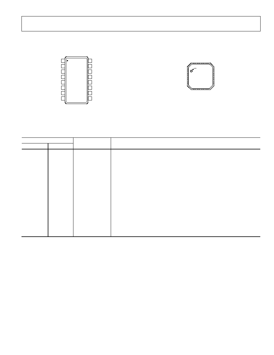
PIN CONFIGURATIONS AND FUNCTION DESCRIPTIONS
TOP VIEW
1
2
3
4
5
6
7
8
ADG1211/
ADG1212/
ADG1213
NC = NO CONNECT
16
15
14
13
12
11
10
9
D1
S1
V
SS
D4
S4
GND
IN1
D2
S2
V
DD
D3
IN4
IN3
S3
NC
IN2
04788-0-002
Figure 2. TSSOP Pin Configuration
PIN 1
INDICATOR
NC = NO CONNECT
1
S1
2
VSS
3
GND
4
S4
11 VDD
12 S2
10 NC
9 S3
5
D
4
6
I
N
4
7
I
N
3
8
D
3
1
5
I
N
1
1
6
D
1
1
4
I
N
2
1
3
D
2
TOP VIEW
(Not to Scale)
04778-0-003
ADG1211/ADG1212/ADG1213
Figure 3. LFCSP Pin Configuration
Table 6. Pin Function Descriptions
Pin No.
TSSOP
LFCSP
Mnemonic Function
1
15
IN1
Logic Control Input.
2
16
D1
Drain Terminal. Can be an input or output.
3
1
S1
Source Terminal. Can be an input or output.
4 2 V
SS
Most Negative Power Supply Potential.
5
3
GND
Ground (0 V) Reference.
6
4
S4
Source Terminal. Can be an input or output.
7
5
D4
Drain Terminal. Can be an input or output.
8
6
IN4
Logic Control Input.
0
7
IN3
Logic Control Input.
10
8
D3
Drain Terminal. Can be an input or output.
11
9
S3
Source Terminal. Can be an input or output.
12 10 NC
No
Connection.
13 11 V
DD
Most Positive Power Supply Potential.
14
12
S2
Source Terminal. Can be an input or output.
15
13
D2
Drain Terminal. Can be an input or output.
16
14
IN2
Logic Control Input.

ADG1211/ADG1212/ADG1213
Preliminary Technical Data
Rev. PrE | Page 8 of 16
TERMINOLOGY
I
DD
The positive supply current.
I
SS
The negative supply current.
V
D
(V
S
)
The analog voltage on Terminals D and S.
R
ON
The ohmic resistance between D and S.
R
FLAT(ON)
Flatness is defined as the difference between the maximum and
minimum value of on resistance, as measured over the specified
analog signal range.
I
S
(Off)
The source leakage current with the switch off.
I
D
(Off)
The drain leakage current with the switch off.
I
D
, I
S
(On)
The channel leakage current with the switch on.
V
INL
The maximum input voltage for Logic 0.
V
INH
The minimum input voltage for Logic 1.
I
INL
(I
INH
)
The input current of the digital input.
C
S
(Off)
The off switch source capacitance, measured with reference to
ground.
C
D
(Off)
The off switch drain capacitance, measured with reference to
ground.
C
D
, C
S
(On)
The on switch capacitance, measured with reference to ground.
C
IN
The digital input capacitance.
t
ON
The delay between applying the digital control input and the
output switching on. See Figure 23.
t
OFF
The delay between applying the digital control input and the
output switching off.
Charge Injection
A measure of the glitch impulse transferred from the digital
input to the analog output during switching.
Off Isolation
A measure of unwanted signal coupling through an off switch.
Crosstalk
A measure of unwanted signal that is coupled through from one
channel to another as a result of parasitic capacitance.
Bandwidth
The frequency at which the output is attenuated by 3 dB.
On Response
The frequency response of the on switch.
Insertion Loss
The loss due to the on resistance of the switch.
Preliminary Technical Data
ADADG1211/ADG1212/ADG1213
Rev. PrE | Page 9 of 16
TYPICAL PERFORMANCE CHARACTERISTICS
Figure 4. On Resistance as a Function of V
D
(V
S
) for Single Supply
Figure 5. On Resistance as a Function of V
D
(V
S
) for Dual Supply
Figure 6. On Resistance as a Function of V
D
(V
S
) for Different Temperatures,
Single Supply
Figure 7. On Resistance as a Function of V
D
(V
S
) for Different Temperatures,
Single Supply
Figure 8. On Resistance as a Function of V
D
(V
S
) for Different Temperatures,
Dual Supply
Figure 9. Leakage Currents as a Function of V
D
(V
S
)
ADG1211/ADG1212/ADG1213
Preliminary Technical Data
Rev. PrE | Page 10 of 16
Figure 10. Leakage Currents as a Function of V
D
(V
S
)
Figure 11. Leakage Currents as a Function of V
D
(V
S
)
Figure 12. Leakage Currents as a Function of Temperature
Figure 13. Leakage Currents as a Function of Temperature
Figure 14. Supply Current vs. Input Switching Frequency
Figure 15. Charge Injection vs. Source Voltage
Preliminary Technical Data
ADADG1211/ADG1212/ADG1213
Rev. PrE | Page 11 of 16
Figure 16. T
ON
/T
OFF
Times vs. Temperature
Figure 17. Off Isolation vs. Frequency
Figure 18. Crosstalk vs. Frequency
Figure 19. On Response vs. Frequency
ADG1211/ADG1212/ADG1213
Preliminary Technical Data
Rev. PrE | Page 12 of 16
TEST CIRCUITS
I
DS
V1
S
D
V
S
R
ON
= V1/I
DS
04778-0-020
S
D
V
S
A
A
V
D
I
S
(OFF)
I
D
(OFF)
04778-0-021
S
D
A
V
D
I
D
(ON)
NC
NC = No Connect
04778-0-022
Figure 20. Test Circuit 1--On Resistance
Figure 21. Test Circuit 2--Off Leakage
Figure 22. Test Circuit 3 --On Leakage
V
S
IN
S
D
GND
R
L
300V
C
L
35pF
V
OUT
V
DD
V
SS
0.1
µ
F
V
DD
0.1
µ
F
V
SS
ADG1211
ADG1212
V
IN
V
IN
V
OUT
t
ON
t
OFF
50%
50%
90%
90%
50%
50%
04778-0-023
Figure 23. Test Circuit 4--Switching Times
V
S2
IN1,
IN2
S2
D2
V
S1
S1
D1
GND
R
L
300V
C
L
35pF
V
OUT2
V
OUT1
V
DD
V
SS
0.1
µ
F
V
DD
0.1
µ
F
V
SS
V
IN
V
OUT1
V
OUT2
ADG1213
t
D
t
D
50%
50%
90%
90%
90%
90%
0V
0V
0V
R
L
300V
C
L
35pF
04778-0-024
Figure 24. Test Circuit 5--Break Before Make Time Delay
IN
V
OUT
ADG1212
ADG1211
V
IN
V
IN
V
OUT
OFF
DV
OUT
ON
Q
INJ
= C
L3
DV
OUT
S
D
V
DD
V
SS
V
DD
V
SS
V
S
R
S
GND
C
L
1nF
04778-0-025
Figure 25. Test Circuit 6--Charge Injection
Preliminary Technical Data
ADADG1211/ADG1212/ADG1213
Rev. PrE | Page 13 of 16
V
OUT
50
NETWORK
ANALYZER
R
L
50
IN
V
IN
S
D
50
OFF ISOLATION = 20 LOG
V
OUT
V
S
V
S
V
DD
V
SS
0.1
µ
F
V
DD
0.1
µ
F
V
SS
GND
04778-0-026
Figure 26. Test Circuit 7--Off Isolation
CHANNEL-TO-CHANNEL CROSSTALK = 20 LOG
V
OUT
GND
S1
D
S2
V
OUT
NETWORK
ANALYZER
R
L
50
R
50
V
S
V
S
V
DD
V
SS
0.1
µ
F
V
DD
0.1
µ
F
V
SS
04778-0-027
Figure 27. Test Circuit 8--Channel-to-Channel Crosstalk
V
OUT
50
NETWORK
ANALYZER
R
L
50
IN
V
IN
S
D
INSERTION LOSS = 20 LOG
V
OUT
WITH SWITCH
V
OUT
WITHOUT SWITCH
V
S
V
DD
V
SS
0.1
µ
F
V
DD
0.1
µ
F
V
SS
GND
04778-0-028
Figure 28. Test Circuit 9--Bandwidth
ADG1211/ADG1212/ADG1213
Preliminary Technical Data
Rev. PrE | Page 14 of 16
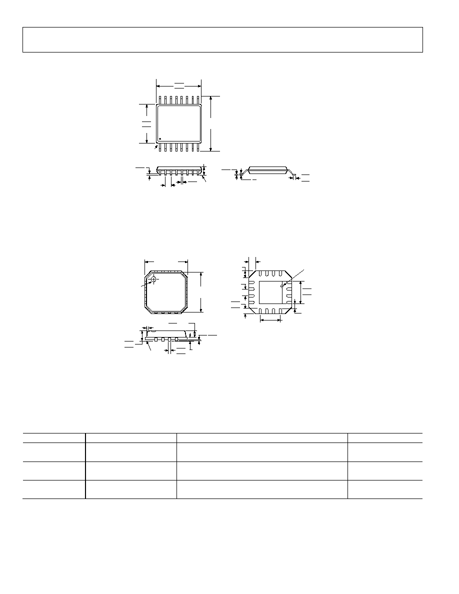
OUTLINE DIMENSIONS
16
9
8
1
PIN 1
SEATING
PLANE
8°
0°
4.50
4.40
4.30
6.40
BSC
5.10
5.00
4.90
0.65
BSC
0.15
0.05
1.20
MAX
0.20
0.09
0.75
0.60
0.45
0.30
0.19
COPLANARITY
0.10
COMPLIANT TO JEDEC STANDARDS MO-153AB
Figure 29. 16-Lead Thin Shrink Small Outline Package [TSSOP]
(RU-16)
Dimensions shown in millimeters
16
5
13
8
9
12
1
4
1.95 BSC
PIN 1
INDICATOR
TOP
VIEW
4.00
BSC SQ
3.75
BSC SQ
COPLANARITY
0.08
EXPOSED
PAD
(BOTTOM VIEW)
COMPLIANT TO JEDEC STANDARDS MO-220-VGGC
12° MAX
1.00
0.85
0.80
SEATING
PLANE
0.30
0.23
0.18
0.80 MAX
0.65 TYP
0.05 MAX
0.02 NOM
0.20 REF
0.65 BSC
0.60 MAX
0.60 MAX
PIN 1
INDICATOR
0.75
0.60
0.50
0.25 MIN
2.25
2.10 SQ
1.95
Figure 30. 16-Lead Lead Frame Chip Scale Package [VQ_LFCSP]
4 mm × 4 mm Body, Very Thin Quad
(CP-16-4)
Dimensions shown in millimeters
ORDERING GUIDE
Model
Temperature Range
Package Description
Package Option
ADG1211YRU
-40°C to +125°C
Thin Shrink Small Outline Package (TSSOP)
RU-16
ADG1211YCP
-40°C to +125°C
Lead Frame Chip Scale Package (LFCSP)
CP-16-4
ADG1212YRU
-40°C to +125°C
Thin Shrink Small Outline Package (TSSOP)
RU-16
ADG1212YCP
-40°C to +125°C
Lead Frame Chip Scale Package (LFCSP)
CP-16-4
ADG1213YRU
-40°C to +125°C
Thin Shrink Small Outline Package (TSSOP)
RU-16
ADG1213YCP
-40°C to +125°C
Lead Frame Chip Scale Package (LFCSP)
CP-16-4

Preliminary Technical Data
ADADG1211/ADG1212/ADG1213
Rev. PrE | Page 15 of 16
NOTES

ADG1211/ADG1212/ADG1213
Preliminary Technical Data
Rev. PrE | Page 16 of 16
NOTES
© 2004 Analog Devices, Inc. All rights reserved. Trademarks and
registered trademarks are the property of their respective owners.
PR04778011/04(PrE)
Document Outline