 | –≠–ª–µ–∫—Ç—Ä–æ–Ω–Ω—ã–π –∫–æ–º–ø–æ–Ω–µ–Ω—Ç: ADIS16003 | –°–∫–∞—á–∞—Ç—å:  PDF PDF  ZIP ZIP |
Document Outline
- FEATURES
- APPLICATIONS
- FUNCTIONAL BLOCK DIAGRAM
- GENERAL DESCRIPTION
- ˛ˇ
- ˛ˇ
- ˛ˇ
- ˛ˇ
- ˛ˇ
- ˛ˇ
- ˛ˇ
- ˛ˇ
Dual-Axis ±1.7 g Accelerometer
with SPI Interface
ADIS16003
Rev. 0
Information furnished by Analog Devices is believed to be accurate and reliable. However, no
responsibility is assumed by Analog Devices for its use, nor for any infringements of patents or other
rights of third parties that may result from its use. Specifications subject to change without notice. No
license is granted by implication or otherwise under any patent or patent rights of Analog Devices.
Trademarks and registered trademarks are the property of their respective owners.
One Technology Way, P.O. Box 9106, Norwood, MA 02062-9106, U.S.A.
Tel: 781.329.4700
www.analog.com
Fax: 781.461.3113
© 2005 Analog Devices, Inc. All rights reserved.
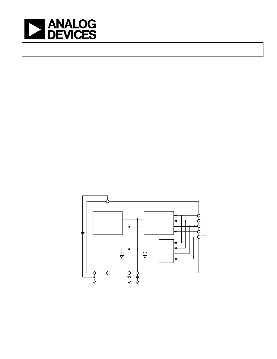
GENERAL DESCRIPTION
FEATURES
Dual-axis accelerometer
The ADIS16003 is a low cost, low power, complete dual-axis
accelerometer with an integrated serial peripheral interface
(SPI). An integrated temperature sensor is also available on the
SPI interface. The ADIS16003 measures acceleration with a full-
scale range of ±1.7 g (minimum), and it can measure both
dynamic acceleration (vibration) and static acceleration
(gravity).
SPIÆ digital output interface
Internal temperature sensor
Highly integrated; minimal external components;
bandwidth externally selectable
1 mg resolution at 60 Hz
Externally controlled electrostatic self-test
3.0 V to 5.25 V single-supply operation
The typical noise floor is 110 g/Hz, allowing signals below
1 mg (60 Hz bandwidth) to be resolved.
Low power: <2 mA
3500 g shock survival
7.2 mm ◊ 7.2 mm ◊ 3.6 mm package
The bandwidth of the accelerometer is set with optional capaci-
tors C
X
and C
Y
at the XFILT and YFILT pins. Selection of the
two analog input channels is controlled via the serial interface.
APPLICATIONS
Industrial vibration/motion sensing
An externally driven self-test pin (ST) allows the user to verify
the accelerometer functionality.
Platform stabilization
Dual-axis tilt sensing
Tracking, recording, analysis devices
The ADIS16003 is available in a 7.2 mm ◊ 7.2 mm ◊ 3.6 mm,
12-terminal LGA package.
Alarms, security devices
FUNCTIONAL BLOCK DIAGRAM
SCLK
DIN
DOUT
CS
TCS
TEMP
SENSOR
SERIAL
INTERFACE
DUAL-AXIS
±
1.7g
ACCELEROMETER
V
CC
C
DC
COM
ST
C
Y
C
X
YFILT
XFILT
056463-001
Figure 1.

ADIS16003
Rev. 0 | Page 2 of 16
TABLE OF CONTENTS
Specifications..................................................................................... 3
Timing Specifications .................................................................. 4
Circuit and Timing Diagrams..................................................... 5
Absolute Maximum Ratings............................................................ 6
ESD Caution.................................................................................. 6
Pin Configuration and Function Descriptions............................. 7
Typical Performance Characteristics ............................................. 8
Theory of Operation ...................................................................... 11
Self-Test........................................................................................ 11
Serial Interface ............................................................................ 11
Accelerometer Serial Interface.................................................. 11
Temperature Sensor Serial Interface........................................ 12
Power Supply Decoupling ......................................................... 13
Setting the Bandwidth Using C
and C
XFILT
YFILT
....................... 13
Selecting Filter Characteristics:
The Noise/Bandwidth Trade-Off ............................................. 13
Applications..................................................................................... 14
Dual-Axis Tilt Sensor ................................................................ 14
Second-Level Assembly ............................................................. 14
Outline Dimensions ....................................................................... 15
Ordering Guide .......................................................................... 15
REVISION HISTORY
10/05--Revision 0: Initial Version

ADIS16003
Rev. 0 | Page 3 of 16
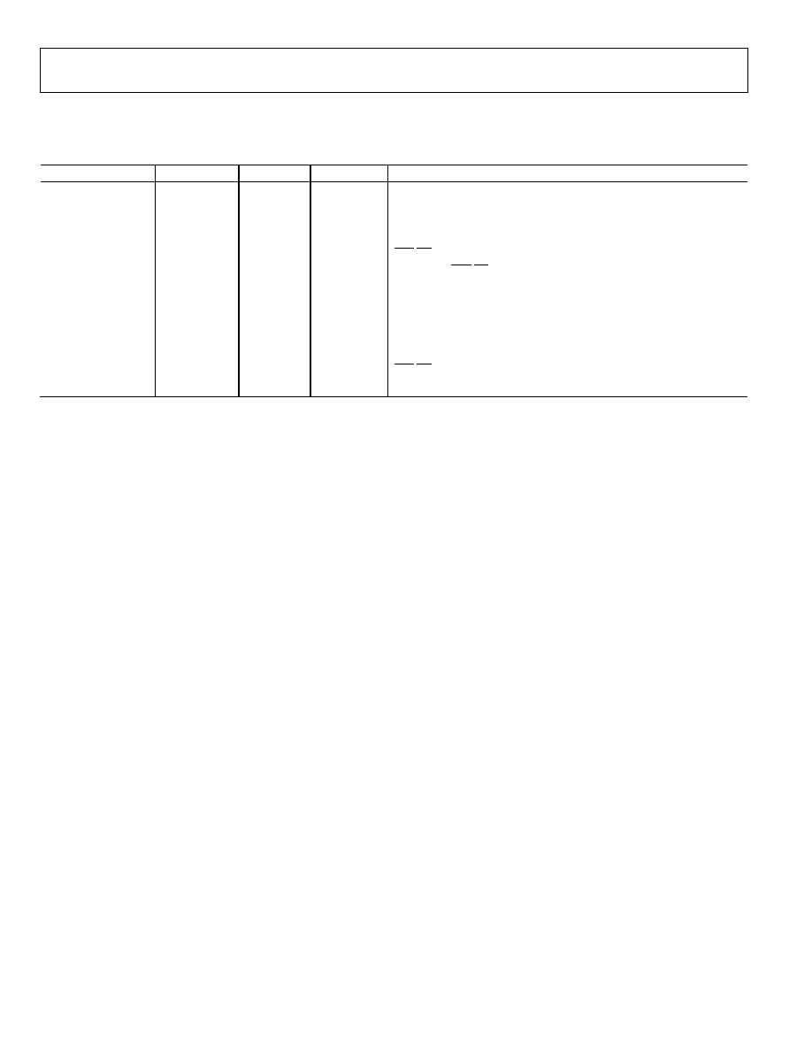
SPECIFICATIONS
T
A
= ≠40∞C to +125∞C, V
CC
= 5 V, C
X
, C
Y
= 0 F, acceleration = 0 g, unless otherwise noted. All minimum and maximum specifications are
guaranteed. Typical specifications are not guaranteed.
Table 1.
Parameter Conditions
Min
Typ
Max
Unit
ACCELEROMETER SENSOR INPUT
Each axis
Measurement Range
1
±1.7
g
Nonlinearity
% of full scale
±0.5
±2.5
%
Package Alignment Error
±1.5
degrees
Alignment Error
X sensor to Y sensor
±0.1
degrees
Cross Axis Sensitivity
±2
±5
%
ACCELEROMETER SENSITIVITY
Each axis
Sensitivity at XFILT, YFILT
769
820
885
LSB/g
Sensitivity Change due to Temperature
2
Delta from 25∞C
±8
LSB
ZERO g BIAS LEVEL
Each axis
0 g Voltage at XFILT, YFILT
1905
2048
2190
LSB
0 g Offset vs. Temperature
±0.14
LSB/∞C
ACCELEROMETER NOISE PERFORMANCE
Noise Density
@25∞C
110
g/Hz rms
ACCELEROMETER FREQUENCY RESPONSE
3
C
X
, C
Y
Range
4
0
10
F
R
FILT
Tolerance
24
32
40
k
Sensor Resonant Frequency
5.5
kHz
ACCELEROMETER SELF-TEST
Logic Input Low
0.2 ◊ V
CC
V
Logic Input High
0.8 ◊ V
CC
V
ST Input Resistance to COM
30
50
k
Output Change at X
OUT
, Y
OUT
T
5
Self-Test 0 to Self-Test 1
323
614
904
LSB
TEMPERATURE SENSOR
Accuracy V
CC
= 3 V to 5.25 V
±2
∞C
Resolution
10
Bits
Update Rate
400
s
Temperature Conversion Time
25
s
DIGITAL INPUT
Input High Voltage (V
INH
) V
CC
= 4.75 V to 5.25 V
2.4
V
V
CC
= 3.0 V to 3.6 V
2.1
V
Input Low Voltage (V
INL
) V
CC
= 3.0 V to 5.25 V
0.8
V
Input Current
V
IN
= 0 V or V
CC
-10 1 10 A
Input Capacitance
10
pF
DIGITAL OUTPUT
Output High Voltage (V
OH
)
I
SOURCE
= 200 A,
V
CC
= 3.0 V to 5.25 V
V
CC
≠ 0.5
V
Output Low Voltage (V
OL
) I
SINK
= 200 A
0.4
V
POWER SUPPLY
Operating Voltage Range
3.0
5.25
V
Quiescent Supply Current
F
SCLK
= 50 kSPS
1.5
2.0
mA
Power Down Current
1.0
mA
Turn-On Time
6
C
x
,
C
y
= 0.1 F
20
Ms
1
Guaranteed by measurement of initial offset and sensitivity.
2
Defined as the output change from ambient to maximum temperature or ambient to minimum temperature.
3
Actual bandwidth response controlled by user-supplied external capacitor (C
x
, C
y
).
4
Bandwidth = 1/(2 x 32 k x (2200 pF + C)). For C
x
, C
y
= 0, bandwidth = 2260 Hz. For C
x
, C
y
= 10 F, bandwidth = 0.5 Hz. Min/max values not tested.
5
Self-test response changes as the square of V
cc
.
6
Larger values of C
x
, C
y
increase turn-on time. Turn-on time is approximately 160 x (0.0022 F + C
x
+ C
y
) + 4 ms, where C
x
, C
y
are in F.
ADIS16003
Rev. 0 | Page 4 of 16
TIMING SPECIFICATIONS
T
A
= ≠40∞C to +125∞C, acceleration = 0 g, unless otherwise noted.
Table 2.
Parameter
1 , 2
V
CC
= 3.3
V
CC
= 5
Unit
Description
f
SCLK
3
10 10
kHz
min
2
2
MHz
max
t
CONVERT
14.5 t
SCLK
14.5 t
CSLK
t
ACQ
1.5 t
SCLK
1.5 t
SCLK
Throughput time = t
CONVERT
+ t
ACQ
= 16 t
SCLK
t
1
10 10
ns
min
TCS/CS to SCLK setup time
t
2
4
60 30
ns
max
Delay from TCS/CS until DOUT three-state disabled
t
3
4
100
75
ns max
Data access time after SCLK falling edge
t
4
20
20
ns min
Data setup time prior to SCLK rising edge
t
5
20
20
ns min
Data hold time after SCLK rising edge
t
6
0.4 ◊ t
SCLK
0.4 x t
SCLK
ns min
SCLK high pulse width
t
7
0.4 ◊ t
SCLK
0.4 x t
SCLK
ns min
SCLK low pulse width
t
8
5
80 80
ns
max
TCS/CS rising edge to DOUT high impedance
t
9
5
5
s typ
Power-up time from shutdown
1
Guaranteed by design. All input signals are specified with tr and tf = 5 ns (10% to 90% of V
CC
) and timed from a voltage level of 1.6 V. The 3.3 V operating range spans
from 3.0 V to 3.6 V. The 5 V operating range spans from 4.75 V to 5.25 V.
2
See Figure 3 and Figure 4.
3
Mark/space ratio for the SCLK input is 40/60 to 60/40.
4
Measured with the load circuit in Figure 2 and defined as the time required for the output to cross 0.4 V or 2.0 V with V
CC
= 3.3 V and time for an output to cross 0.8 V or
2.4 V with V
CC
= 5.0 V.
5
t
8
is derived from the measured time taken by the data outputs to change 0.5 V when loaded with the circuit in Figure 2. The measured number is then extrapolated
back to remove the effects of charging or discharging the 50 pF capacitor. This means that the time, t
8
, quoted in the timing characteristics is the true bus relinquish
time of the part and is independent of the bus loading.
ADIS16003
Rev. 0 | Page 5 of 16
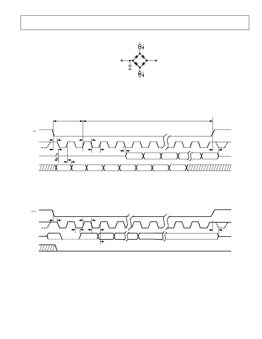
CIRCUIT AND TIMING DIAGRAMS
05463-002
200
A
I
OL
200
A
I
OH
1.6V
TO OUTPUT
PIN
C
L
50pF
Figure 2. Load Circuit for Digital Output Timing Specifications
05463-003
SCLK
DOUT
DIN
DONTC
ZERO
ZERO
ZERO
ADD0
ONE
ZERO
PM0
4 LEADING ZEROS
1
2
3
4
5
6
15
16
t
ACQ
t
CONVERT
THREE-STATE
THREE-STATE
t
1
t
2
t
5
t
4
t
6
t
7
t
3
t
8
DB11
DB10
DB9
DB0
CS
Figure 3. Accelerometer Serial Interface Timing Diagram
05463-004
TCS
SCLK
DOUT
DIN
1
2
3
4
11
15
16
THREE-
STATE
THREE-STATE
t
1
t
6
t
7
t
3
t
8
DB0
DB9
DB8
LEADING
ZERO
Figure 4. Temperature Serial Interface Timing Diagram

ADIS16003
Rev. 0 | Page 6 of 16
ABSOLUTE MAXIMUM RATINGS
Table 3.
Parameter Rating
Stresses above those listed under Absolute Maximum Ratings
may cause permanent damage to the device. This is a stress
rating only; functional operation of the device at these or any
other conditions above those indicated in the operational
section of this specification is not implied. Exposure to absolute
maximum rating conditions for extended periods may affect
device reliability.
Acceleration (Any Axis, Unpowered)
3,500 g
Acceleration (Any Axis, Powered)
3,500 g
V
≠0.3 V to +7.0 V
CC
All Other Pins
(COM ≠ 0.3 V) to
(V + 0.3 V)
CC
Output Short-Circuit Duration
(Any Pin to Common)
Indefinite
Operating Temperature Range
≠40∞C to +125∞C
Storage Temperature
≠65∞C to +150∞C
Table 4. Package Characteristics
Package Type
Device Weight
JA
JC
12-Terminal LGA
200∞C/W
25∞C/W
0.3 grams
ESD CAUTION
ESD (electrostatic discharge) sensitive device. Electrostatic charges as high as 4000 V readily accumulate on
the human body and test equipment and can discharge without detection. Although this product features
proprietary ESD protection circuitry, permanent damage may occur on devices subjected to high energy
electrostatic discharges. Therefore, proper ESD precautions are recommended to avoid performance
degradation or loss of functionality.
1.0755
8
◊
BSC
0.670
8
◊
BSC
1.127
12
◊
BSC
0.500
12
◊
BSC
5.873
2
◊
05463-023
Figure 5. Second-Level Assembly Pad Layout
ADIS16003
Rev. 0 | Page 7 of 16
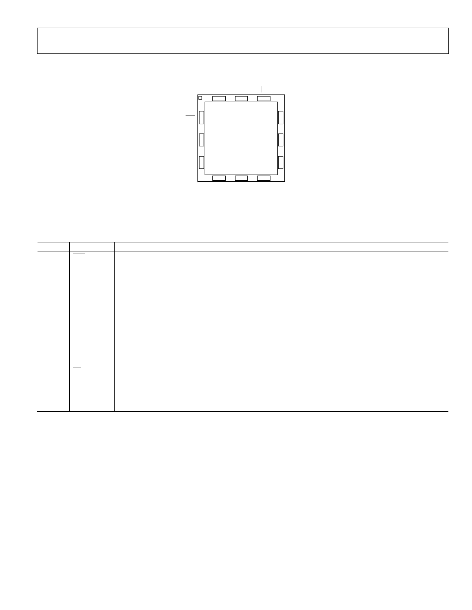
PIN CONFIGURATION AND FUNCTION DESCRIPTIONS
ADIS16003
TOP VIEW
(Not to Scale)
05463-005
N
C
C
O
M
S
T
V
C
C
S
C
L
K
C
S
NC = NO CONNECT
XFILT
YFILT
NC
9
8
2
7
1
3
6
5
4
10
12
11
TCS
DOUT
DIN
Figure 6. Pin Configuration
Table 5. Pin Function Descriptions
Pin No.
Mnemonic
Description
1
TCS
Temperature Chip Select. Active low logic input. This input frames the serial data transfer for the temperature
sensor output.
2 DOUT Data Out, Logic Output. The conversion of the ADIS16003 is provided on this output as a serial data stream.
The bits are clocked out on the falling edge of the SCLK input.
3 DIN Data In, Logic Input. Data to be written into the ADIS16003's control register is provided on this input and
is clocked into the register on the rising edge of SCLK.
4
COM
Common. Reference point for all circuitry on the ADIS16003.
5, 7
NC
No Connect.
6
ST
Self-Test Input. Active high logic input. Simulates a nominal 0.75 g test input for diagnostic purpose.
8 YFILT Y Channel Filter Node. Used in conjunction with an optional external capacitor to band-limit the ac signal
from the accelerometer.
9 XFILT X Channel Filter Node. Used in conjunction with an optional external capacitor to band-limit the ac signal
from the accelerometer.
10
CS
Chip Select. Active low logic input. This input provides the dual function of initiating the accelerometer
conversions on the ADIS16003 and frames the serial data transfer for the accelerometer output.
11 V
CC
Power Supply Input. The V range for the ADIS16003 is from 3.0 V to 5.25 V.
CC
12 SCLK Serial Clock, Logic Input. SCLK provides the serial clock for accessing data from the part and writing serial data
to the control register. This clock input is also used as the clock source for the ADIS16003's conversion process.
ADIS16003
Rev. 0 | Page 8 of 16
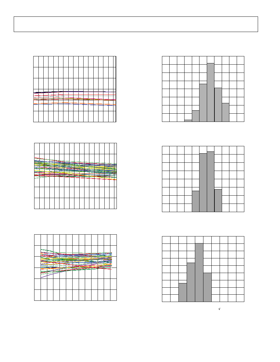
TYPICAL PERFORMANCE CHARACTERISTICS
40
0
1900
05463-009
OUTPUT (LSB)
PER
C
E
N
T
A
GE OF POPU
LA
TION
30
25
20
15
10
5
1929 1958 1987 2016 2045 2074 2103 2132 2161 2190
35
890
770
05463-006
TEMPERATURE (
∞
C)
125
870
850
830
810
790
≠20
0
20
40
60
80
100
≠40
SEN
SITIVITY (
L
SB
/
g
)
Figure 10. X-Axis Zero g Bias at 25∞C
Figure 7. Sensitivity vs. Temperature (AD16003 Soldered to PCB)
2200
1900
≠40
05463-007
TEMPERATURE (
∞
C)
B
IA
S
LEVEL (
L
SB
)
125
2150
2100
2050
2000
1950
≠20
0
20
40
60
80
100
40
0
1990
05463-010
OUTPUT (LSB)
PER
C
E
N
T
A
GE OF POPU
LA
TION
30
25
20
15
10
5
1929 1958 1987 2016 2045 2074 2103 2132 2161 2190
35
Figure 8
.
Zero g Bias vs. Temperature
Figure 11. Y-Axis Zero g Bias at 25∞C
2200
1900
2.8
05463-008
VOLTS
B
IA
S
LEVEL (
L
SB
)
5.4
2150
2100
2050
2000
1950
3.0 3.2 3.4 3.6 3.8 4.0 4.2 4.7 4.6 4.8 5.0 5.2
45
0
05463-011
X-AXIS NOISE DENSITY (
g/ Hz)
PER
C
E
N
T
A
GE OF POPU
LA
TION
40
35
30
25
20
15
10
5
60
70
80
90
100
110
120
130
140
150
Figure 9. Zero g Bias vs. Supply
Figure 12. X-Axis Noise Density at 25∞C
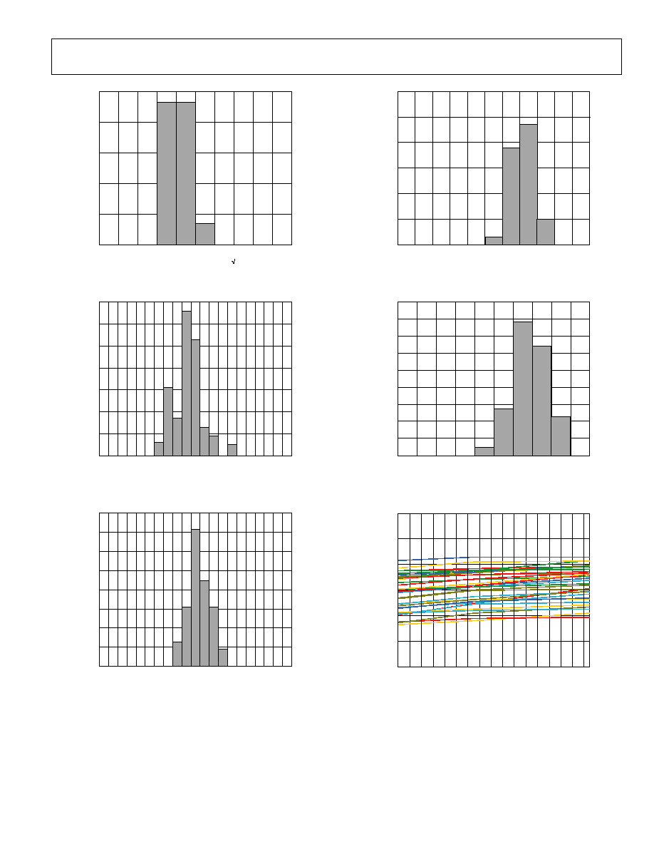
ADIS16003
Rev. 0 | Page 9 of 16
50
0
05463-012
Y-AXIS NOISE DENSITY (
g/ Hz)
PER
C
E
N
T
A
GE OF POPU
LA
TION
60
70
80
90
100
110
120
130
140
150
40
30
20
10
60
0
05463-015
OUTPUT (LSB)
PER
C
E
N
T
A
GE OF POPU
LA
TION
350
850
40
30
20
10
400 450 500 550 600 650 700 750 800
50
Figure 13. Y-Axis Noise Density at 25∞C
Figure 16. Self-Test at 25∞C, V
CC
at 5.0 V
35
0
05463-013
PERCENT SENSITIVITY (%)
PER
C
E
N
T
A
GE OF POPU
LA
TION
≠4.5 ≠3.5 ≠2.5 ≠1.5 ≠0.5
0.5
1.5
2.5
3.5
4.5
5.5
30
25
20
15
10
5
45
0
05463-016
OUTPUT (LSB)
PER
C
E
N
T
A
GE OF POPU
LA
TION
315
40
30
25
20
15
10
5
180
195
210
225
240
255
270
285
300
35
Figure 14. Z vs. X Cross-Axis Sensitivity
Figure 17. Self-Test at 25∞C, V
CC
at 3.3 V
40
0
05463-014
PERCENT SENSITIVITY (%)
PER
C
E
N
T
A
GE OF POPU
LA
TION
≠4.5 ≠3.5 ≠2.5 ≠1.5 ≠0.5
0.5
1.5
2.5
3.5
4.5
5.5
35
30
25
20
15
10
5
750
450
≠40
05463-017
TEMPERATURE (
∞
C)
SELF-
TEST LEVEL (
L
SB
/
g
)
125
700
650
600
550
500
≠20
0
20
40
60
80
100
Figure 15. Z vs. Y Cross-Axis Sensitivity
Figure 18. Self-Test vs. Temperature V
CC
at 5.0 V
ADIS16003
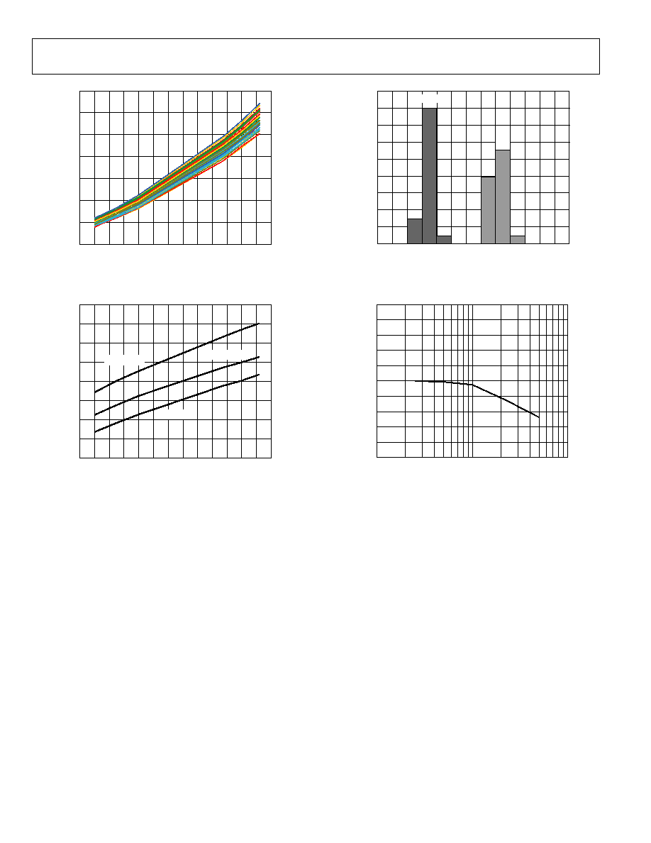
Rev. 0 | Page 10 of 16
800
100
05463-018
VOLTS
SELF-
TEST LEVEL (
L
SB
)
5.4
2.8 3.0 3.2 3.4 3.6 3.8 4.0 4.2 4.4 4.6 4.8 5.0 5.2
700
600
500
400
300
200
90
0
05463-020
CURRENT (
A)
PER
C
E
N
T
A
GE OF POPU
LA
TION
1.75
50
40
30
20
10
1.15 1.20 1.25 1.30 1.35 1.40 1.45 1.50 1.55 1.60 1.65 1.70
3.3V
5V
80
70
60
Figure 21. Supply Current at 25∞C
Figure 19. Self-Test vs. Supply Voltage
1.0
≠1.0
05463-021
SAMPLE RATE (kSPS)
S
A
MP
LING E
RROR (dB)
100
1
0.8
0.6
0.4
0.2
0
≠0.2
≠0.4
≠0.6
≠0.8
10
1.8
1.0
05463-019
VOLTS
CURRE
NT (mA)
5.4
2.8 3.0 3.2 3.4 3.6 3.8 4.0 4.2 4.4 4.6 4.8 5.0 5.2
T
A
= +25∞C
T
A
= ≠40∞C
1.7
1.6
1.5
1.4
1.3
1.2
1.1
T
A
= +125∞C
Figure 22. Sampling Error vs. Sample Rate
Figure 20. Supply Current vs. Supply Voltage

ADIS16003
Rev. 0 | Page 11 of 16
THEORY OF OPERATION
ACCELEROMETER SERIAL INTERFACE
12
4
10
11
6
5
8
9
7
3
2
1
12
4
10
11
6
5
8
9
7
3
2
1
12
4
10
11
6
5
8
9
7
3
2
1
12
4
10
11
6
5
8
9
7
3
2
1
Top View
Not to Scale
DIGITAL OUTPUT (IN LSBs)
X-AXIS: 1229
Y-AXIS: 2048
DIGITAL OUTPUT (IN LSBs)
X-AXIS: 2867
Y-AXIS: 2048
DIGITAL OUTPUT (IN LSBs)
X-AXIS: 2048
Y-AXIS: 2867
DIGITAL OUTPUT (IN LSBs)
X-AXIS: 2048
Y-AXIS: 1229
DIGITAL OUTPUT (IN LSBs)
X-AXIS: 2048
Y-AXIS: 2048
05463-
024
Figure 3 shows the detailed timing diagram for serial inter-
facing to the accelerometer in the ADIS16003. The serial clock
provides the conversion clock. CS initiates the data transfer and
conversion process
and frames the serial data transfer for the
accelerometer output. The accelerometer output is sampled on
the second rising edge of the SCLK input after the falling edge
of the CS. The conversion requires 16 SCLK cycles to complete.
The rising edge of
Figure 23. Output Response vs. Orientation
The ADIS16003 is a low cost, low power, complete dual-axis
accelerometer with an integrated serial peripheral interface
(SPI) and an integrated temperature sensor whose output is also
available on the SPI interface. The ADIS16003 is capable of
measuring acceleration with a full-scale range of ±1.7 g
(minimum). It can also measure both dynamic acceleration
(vibration) and static acceleration (gravity).
SELF-TEST
The ST pin controls the self-test feature. When this pin is set to
V
CC
, an electrostatic force is exerted on the beam of the acceler-
ometer. The resulting movement of the beam allows the user to
test if the accelerometer is functional. The typical change in
output is 750 mg (corresponding to 614 LSB) for V
CC
= 5.0 V.
This pin may be left open-circuit or connected to common in
normal use. The ST pin should never be exposed to voltage
greater than V
CC
+ 0.3 V. If the system design is such that this
condition cannot be guaranteed (for example, multiple supply
voltages present), a low V
F
clamping diode between ST and V
CC
is recommended.
SERIAL INTERFACE
The serial interface on the ADIS16003 consists of five wires, CS,
TCS, SCLK, DIN, and DOUT, with the temperature sensor's
serial interface in parallel with the accelerometer's serial
interface. The CS and TCS are used to select the accelerometer
or temperature sensor outputs, respectively. CS and TCS cannot
be active at the same time.
The SCLK input accesses data from the internal data registers.
CS
CS
puts the bus back into three-state. If
remains low, the next digital conversion is initiated. The details
for the control register bit functions are shown in Table 6.
Accelerometer Control Register
MSB
LSB
DONTC ZERO ZERO ZERO ADD0 ONE ZERO PM0
Table 6. Accelerometer Control Register Bit Functions
Bit Mnemonic Comments
7
DONTC
Don't care. Can be one or zero.
ZERO
These bits should be held low.
6, 5,
4
3 ADD0
This address bit selects the x-axis or y-axis
outputs. Zero selects the x-axis; one selects
the y-axis.
2
ONE
This bit should be held high.
1
ZERO
This bit should be held low.
0 PM0
This bit selects the operation mode for the
accelerometer; set to zero for normal
operation and one for power down mode.
Power Down
By setting PM0 to one when updating the accelerometer control
register, the ADIS16003 goes into a shutdown mode. The
information stored in the control register is maintained during
shutdown. The ADIS16003 changes modes as soon as the
control register is updated. If the part is in shutdown mode and
PM0 is changed to zero, then the part powers up on the
sixteenth SCLK rising edge.
ADD0
By setting ADD0 to zero when updating the accelerometer
control register, the x-axis output is selected. By setting ADD0
to one, the y-axis output is selected.
ZERO
ZERO is defined as the logic low level.
ONE
ONE is defined as the logic high level.
DONTC
DONTC is defined as don't care; can be a low or high logic level.
ADIS16003
Rev. 0 | Page 12 of 16
Accelerometer Conversion Details
Every time the accelerometer is sampled, the sampling function
discharges the internal C
X
or C
Y
filtering capacitors by up to 2%
of their initial values (assuming no additional external filtering
capacitors have been added). The recovery time for the filter
capacitor to recharge is approximately 10 s. Thus, sampling the
accelerometer at a rate of 10 kSPS or less does not induce a
sampling error. However, as sampling frequencies increase
above 10 kSPS, one can expect sampling errors to attenuate the
actual acceleration levels.
TEMPERATURE SENSOR SERIAL INTERFACE
Read Operation
Figure 4 shows the timing diagram for a serial read from the
temperature sensor. The TCS line enables the SCLK input. Ten
bits of data and a leading zero are transferred during a read
operation. Read operations occur during streams of 16 clock
pulses. The serial data is accessed in a number of bytes if 10 bits
of data are being read. At the end of the read operation, the
DOUT line remains in the state of the last bit of data clocked
out until TCS goes high, at which time the DOUT line from
the temperature sensor goes three-state.
Write Operation
Figure 4 also shows the timing diagram for the serial write
to the temperature sensor. The write operation takes place at
the same time as the read operation. Data is clocked into the
control register on the rising edge of SCLK. DIN should remain
low for the entire cycle.
Temperature Sensor Control Register
MSB
LSB
ZERO ZERO ZERO ZERO ZERO ZERO ZERO ZERO
Table 7. Temperature Sensor Control Register Bit Functions
Bit Mnemonic Comments
7 to 0
ZERO
All bits should be held low.
ZERO
ZERO is defined as the logic low level.
Output Data Format
The output data format for the temperature sensor is twos
complement. Table 8 shows the relationship between the digital
output and the temperature.
Temperature Sensor Conversion Details
The ADIS16003 features a 10-bit digital temperature sensor
that allows an accurate measurement of the ambient device
temperature to be made.
The conversion clock for the temperature sensor is internally
generated so no external clock is required except when reading
from and writing to the serial port. In normal mode, an internal
clock oscillator runs the automatic conversion sequence.
A conversion is initiated approximately every 350 s. At this
time, the temperature sensor wakes up and performs a tempera-
ture conversion. This temperature conversion typically takes
25 s, at which time the temperature sensor automatically shuts
down. The result of the most recent temperature conversion is
available in the serial output register at any time. Once the
conversion is finished, an internal oscillator starts counting and
is designed to time out every 350 s. The temperature sensor
then powers up and does a conversion. Note that if the TCS is
brought low every 350 s (±30%) or less, then the same
temperature value is output onto the DOUT line every time
without changing. It is recommended that the TCS line not be
brought low every 350 s (±30%) or less. The ±30% covers
process variation. The TCS should become active (high to low)
outside this range.
The device is designed to auto convert every 350 s. If the
temperature sensor is accessed during the conversion process,
an internal signal is generated to prevent any update of the
temperature value register during the conversion. This prevents
the user from reading back spurious data. The design of this
feature results in this internal lockout signal being reset only at
the start of the next auto conversion. Therefore, if the TCS line
goes active before the internal lockout signal is reset to its
inactive mode, the internal lockout signal is not reset. To ensure
that no lockout signal is set, bring TCS low at a greater time
than 350 s (±30%). As a result, the temperature sensor is not
interrupted during a conversion process.
In the automatic conversion mode, every time a read or write
operation takes place, the internal clock oscillator is restarted at
the end of the read or write operation. The result of the conver-
sion is typically available 25 s later. Reading from the device
before conversion is complete provides the same set of data.
Table 8. Temperature Sensor Data Format
Temperature
Digital Output (DB9 ... DB0)
≠40∞C
11 0110 0000
≠25∞C
11 1001 1100
≠0.25∞C
11 1111 1111
0∞C
00 0000 0000
+0.25∞C
00 0000 0001
+10∞C
00 0010 1000
+25∞C
00 0110 0100
+50∞C
00 1100 1000
+75∞C
01 0010 1100
+100∞C
01 1001 0000
+125∞C
01 1111 0100

ADIS16003
Rev. 0 | Page 13 of 16
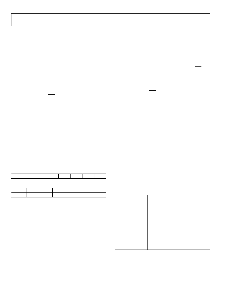
POWER SUPPLY DECOUPLING
For most applications, a single 0.1 F capacitor (C
DC
) adequately
decouples the accelerometer from noise on the power supply.
However, in some cases, particularly where noise is present at
the 140 kHz internal clock frequency (or any harmonic
thereof), noise on the supply may cause interference on the
ADIS16003 output. If additional decoupling is needed, ferrite
beads may be inserted in the supply line of the ADIS16003.
Additionally, a larger bulk bypass capacitor (in the 1 F to 22 F
range) may be added in parallel to C
DC.
SETTING THE BANDWIDTH USING C
XFILT
AND C
YFILT
The ADIS16003 has provisions for band-limiting the acceler-
ometer. Capacitors can be added at the XFILT and YFILT pins
to implement further low-pass filtering for antialiasing and
noise reduction. The equation for the 3 dB bandwidth is
F
-3dB
= 1/(2(32 k) ◊ (C
(XFILT, YFILT)
+ 2200 pF))
or more simply,
F
-3dB
= 5 F/(C
(XFILT, YFILT)
+ 2200 pF)
The tolerance of the internal resistor (R
FILT
) can vary typically as
much as ±25% of its nominal value (32 k); thus, the band-
width varies accordingly.
A minimum capacitance of 0 pF for C
XFILT
and C
YFILT
is
allowable.
Table 9. Filter Capacitor Selection, C
XFILT
and C
YFILT
Bandwidth (Hz)
Capacitor (F)
1
4.7
10
0.47
50
0.10
100 0.047
200 0.022
400 0.01
2250 0
SELECTING FILTER CHARACTERISTICS:
THE NOISE/BANDWIDTH TRADE-OFF
The accelerometer bandwidth selected ultimately determines
the measurement resolution (smallest detectable acceleration).
Filtering can be used to lower the noise floor, which improves
the resolution of the accelerometer. Resolution is dependent
on the analog filter bandwidth at XFILT and YFILT.
The ADIS16003 has a typical bandwidth of 2.25 kHz with no
external filtering. The analog bandwidth may be further
decreased to reduce noise and improve resolution.
The ADIS16003 noise has the characteristics of white Gaussian
noise, which contributes equally at all frequencies and is
described in terms of g/Hz (that is, the noise is proportional
to the square root of the accelerometer's bandwidth). The user
should limit bandwidth to the lowest frequency needed by the
application in order to maximize the resolution and dynamic
range of the accelerometer.
With the single pole roll-off characteristic, the typical noise of
the ADIS16003 is determined by
rmsNoise = (110 g/Hz) x ((BW x 1.6))
At 100 Hz, the noise is
rmsNoise = (110 g/Hz) x ((100 x 1.6)) =1.4 mg
Often, the peak value of the noise is desired. Peak-to-peak noise
can only be estimated by statistical methods. Table 10 is useful
for estimating the probabilities of exceeding various peak
values, given the rms value.
Table 10. Estimation of Peak-to-Peak Noise
Peak-to-Peak
Value
Percentage of Time that Noise Exceeds
Nominal Peak-to-Peak Value
2 ◊ rms
32%
4 ◊ rms
4.6%
6 ◊ rms
0.27%
8 ◊ rms
0.006%
ADIS16003
Rev. 0 | Page 14 of 16
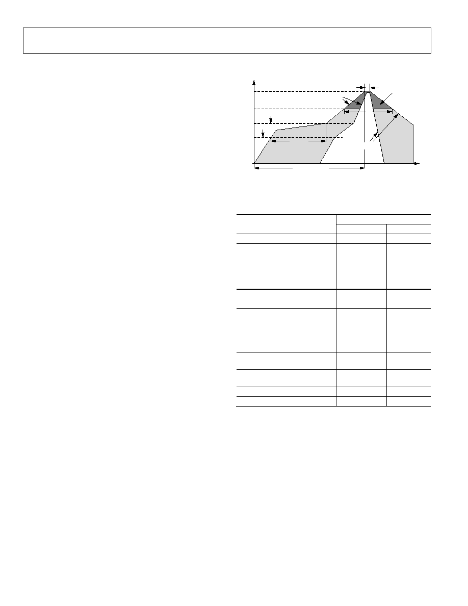
APPLICATIONS
DUAL-AXIS TILT SENSOR
05463-022
t
P
t
L
t
25∞C TO PEAK
t
S
PREHEAT
CRITICAL ZONE
T
L
TO T
P
TEMPERATURE
TIME
RAMP-DOWN
RAMP-UP
T
SMIN
T
SMAX
T
P
T
L
One of the most popular applications of the ADIS16003 is tilt
measurement. An accelerometer uses the force of gravity as an
input vector to determine the orientation of an object in space.
An accelerometer is most sensitive to tilt when its sensitive axis
is perpendicular to the force of gravity, that is, parallel to the
earth's surface. At this orientation, its sensitivity to changes in
tilt is highest. When the accelerometer is oriented on axis to
gravity, near its +1 g or ≠1 g reading, the change in output
acceleration per degree of tilt is negligible. When the acceler-
ometer is perpendicular to gravity, its output changes nearly
17.5 mg per degree of tilt. At 45∞, its output changes at only
12.2 mg per degree, and resolution declines.
Figure 24. Acceptable Solder Reflow Profiles
Table 11.
Converting Acceleration to Tilt
Condition
When the accelerometer is oriented so both its x-axis and y-axis
are parallel to the earth's surface, it can be used as a 2-axis tilt
sensor with a roll axis and a pitch axis. Once the output signal
from the accelerometer has been converted to an acceleration
that varies between ≠1 g and +1 g, the output tilt in degrees is
calculated as follows:
PITCH = Asin(A
X
/1 g)
ROLL = Asin(A
Y
/1 g)
Be sure to account for overranges. It is possible for the
accelerometers to output a signal greater than ±1 g due to
vibration, shock, or other accelerations.
SECOND-LEVEL ASSEMBLY
The ADIS16003 may be attached to the second-level assembly
board using SN63 (or equivalent) or lead-free solder. Figure 24
and Table 11 provide acceptable solder reflow profiles for each
solder type. Note: These profiles may not be the optimum
profile for the user's application. In no case should 260∞C be
exceeded. It is recommended that the user develop a reflow
profile based upon the specific application. In general, keep in
mind that the lowest peak temperature and shortest dwell time
above the melt temperature of the solder results in less shock
and stress to the product. In addition, evaluating the cooling
rate and peak temperature can result in a more reliable
assembly.
Profile Feature
Sn63/Pb37
Pb-free
Average Ramp Rate (T
L
to T
P
)
3∞C/sec max
3∞C/sec max
Preheat
Minimum Temperature (T
SMIN
) 100∞C
150∞C
Maximum Temperature (T
SMAX
) 150∞C
200∞C
Time (T
SMIN to
T
SMAX
) (t
s
)
60 sec to
120 sec
60 sec to
150 sec
T
SMAX
to T
L
Ramp-Up Rate
3∞C/sec
3∞C/sec
Time Maintained Above
Liquidous (T
L
)
Liquidous Temperature (T
L
) 183∞C
217∞C
Time (t
L
)
60 sec to
150 sec
60 sec to
150 sec
Peak Temperature (T )
240∞C +
0∞C/≠5∞C
260∞C +
0∞C/≠5∞C
P
10 sec to
30 sec
20 sec to
40 sec
Time Within 5∞C of Actual Peak
Temperature (t
p
)
Ramp-Down Rate
6∞C/sec max
6∞C/sec max
Time 25∞C to Peak Temperature
6 min max
8 min max

ADIS16003
Rev. 0 | Page 15 of 16
OUTLINE DIMENSIONS
TOP VIEW
PIN 1
INDICATOR
7.327
MAX SQ
5.00 TYP
BOTTOM VIEW
1.302
BSC
0.373
BSC
0.227
BSC
PIN 1
INDICATOR
0.797
BSC
1.00
BSC
3.60
MAX
1
3
9
7
4
6
12
10
Figure 25. 12-Terminal Land Grid Array [LGA]
(CC-12)
Dimensions shown in millimeters
ORDERING GUIDE
Model
Temperature Range
Package Description
Package Option
ADIS16003CCCZ
-40∞C to +125∞C
12-Terminal Land Grid Array (LGA)
CC-12
1
ADIS16003/PCB
Evaluation
Board
1
Z = Pb-free part.

ADIS16003
Rev. 0 | Page 16 of 16
NOTES
© 2005 Analog Devices, Inc. All rights reserved. Trademarks and
registered trademarks are the property of their respective owners.
D05463-0-
10/05(0)