 | –≠–ª–µ–∫—Ç—Ä–æ–Ω–Ω—ã–π –∫–æ–º–ø–æ–Ω–µ–Ω—Ç: ADIS16100 | –°–∫–∞—á–∞—Ç—å:  PDF PDF  ZIP ZIP |
Document Outline
- ˛ˇ
- ˛ˇ
- ˛ˇ
- ˛ˇ
- ˛ˇ
- ˛ˇ
- ˛ˇ
- ˛ˇ
- ˛ˇ
- ˛ˇ
- ˛ˇ
- ˛ˇ
- ˛ˇ
- ˛ˇ
- ˛ˇ
- ˛ˇ
- ˛ˇ
- ˛ˇ
- ˛ˇ
- ˛ˇ
- ˛ˇ
±300∞/sec Yaw Rate
Gyro
with SPI Interface
ADIS16100
Rev. A
Information furnished by Analog Devices is believed to be accurate and reliable. However, no
responsibility is assumed by Analog Devices for its use, nor for any infringements of patents or other
rights of third parties that may result from its use. Specifications subject to change without notice. No
license is granted by implication or otherwise under any patent or patent rights of Analog Devices.
Trademarks and registered trademarks are the property of their respective owners.
One Technology Way, P.O. Box 9106, Norwood, MA 02062-9106, U.S.A.
Tel: 781.329.4700
www.analog.com
Fax: 781.461.3113
©2006 Analog Devices, Inc. All rights reserved.
FEATURES
GENERAL DESCRIPTION
Complete angular rate gyroscope
The ADIS16100 is a complete angular rate sensor (gyroscope)
that uses the Analog Devices surface-micromachining process
to make a functionally complete angular rate sensor with an
integrated serial peripheral interface (SPI).
Z-axis (yaw rate) response
SPIÆ digital output interface
High vibration rejection over wide frequency
2000 g powered shock survivability
The digital data available at the SPI port is proportional to the
angular rate about the axis normal to the top surface of the
package (see
Externally controlled self test
Internal temperature sensor output
Figure 19). A single external resistor can be used to
increase the measurement range. An external capacitor can be
used to lower the bandwidth.
Dual auxiliary 12-bit ADC inputs
Absolute rate output for precision applications
5 V single-supply operation
8.2 mm ◊ 8.2 mm ◊ 5.2 mm package
Access to an internal temperature sensor measurement is
provided, through the SPI, for compensation techniques.
Two pins are available to the user to input analog signals for
digitization. An additional output pin provides a precision
voltage reference. Two digital self-test inputs electro-
mechanically excite the sensor to test operation of the
sensor and the signal conditioning circuits.
APPLICATIONS
Platform stabilization
Image stabilization
Guidance and control
Inertial measurement units
The ADIS16100 is available in an 8.2 mm ◊ 8.2 mm ◊ 5.2 mm,
16-terminal, peripheral land grid array (LGA) package.
FUNCTIONAL BLOCK DIAGRAM
SCLK
DIN
DOUT
CS
V
CC
+5V
ST1
FILT
ST2
COM
4-CHANNEL
SPI
±300∞/s
GYROSCOPE
AIN2
AIN1
TEMP
SENSOR
05
46
1-
00
1
MUX/ADC
ADIS16100
REF
V
REF
V
DRIVE
+3V TO +5V
RATE
C
OUT
Figure 1.

ADIS16100
Rev. A | Page 2 of 16
TABLE OF CONTENTS
Features .............................................................................................. 1
Applications....................................................................................... 1
General Description ......................................................................... 1
Functional Block Diagram .............................................................. 1
Revision History ............................................................................... 2
Specifications..................................................................................... 3
Timing Diagram ........................................................................... 4
Timing Specifications...............................
....................................... 5
Absolute Maximum Ratings............................................................ 6
ESD Caution.................................................................................. 6
Pin Configuration and Function Descriptions............................. 7
Typical Performance Characteristics ............................................. 8
Theory of Operation ...................................................................... 11
Supply and Common Considerations ..................................... 11
Increasing Measurement Range ............................................... 11
Setting Bandwidth...................................................................... 11
Self-Test Function ...................................................................... 11
Continuous Self Test .................................................................. 11
Control Register ......................................................................... 12
Serial Interface ............................................................................ 13
Rate Sensitive Axis ..................................................................... 13
Second-Level Assembly ............................................................. 14
Outline Dimensions ....................................................................... 15
Ordering Guide .......................................................................... 15
REVISION HISTORY
5/06--Rev. 0 to Rev. A
Changes to Table 1............................................................................ 4
Changes to Setting Bandwidth Section........................................ 11
Changes to Table 9 and Table 10................................................... 13
1/06--Revision 0: Initial Version

ADIS16100
Rev. A | Page 3 of 16
SPECIFICATIONS
T
A
= 25∞C, V
CC
= V
DR
= 5 V, angular rate = 0∞/sec, C
OUT
= 0 F, ±1 g, unless otherwise noted.
Table 1.
Parameter Conditions Mi
n
1
Typ Max
1
Unit
SENSITIVITY
Clockwise rotation is positive output
Dynamic Range
2
Full-scale range over specifications range
±300
∞/sec
Initial @
25∞C
3.68
4.1
4.52
LSB/∞/sec
Change Over Temperature
3
V
CC
= V
DRIVE
= 4.75 V to 5.25 V
±10
%
Nonlinearity
Best fit straight line
0.15
% of FS
NULL
Initial Null
1876
2048
2200
LSB
Change Over Temperature
3
V
CC
= V
DR
= 4.75 V to 5.25 V
±205
LSB
Turn-On Time
Power on to ±Ω∞/sec of final
75
ms
Linear Acceleration Effect
Any axis
0.82
LSB/g
Voltage Sensitivity
V
CC
= V
DRIVE
= 4.75 V to 5.25 V
4.1
LSB/V
NOISE PERFORMANCE
0.1 Hz to 40 Hz
3.25
LSB rms
Rate Noise Density
f = 100 Hz
0.43
LSB rms/Hz
FREQUENCY RESPONSE
3 dB Bandwidth (User-Selectable)
4
C
OUT
= 0 F
40
Hz
Sensor Resonant Frequency
14
kHz
SELF-TEST INPUTS
ST1 RATEOUT Response
5
ST1 pin from Logic 0 to Logic 1
-121
-221
-376
LSB
ST2 RATEOUT Response
5
ST2 pin from Logic 0 to Logic 1
+121
+221
+376
LSB
Logic 1 Input Voltage
Standard high logic level definition
3.3
V
Logic 0 Input Voltage
Standard low logic level definition
1.7
V
Input Impedance
To common
50
k
TEMPERATURE SENSOR
Reading at 298 K
2048
LSB
Scale Factor
Proportional to absolute temperature
6.88
LSB/K
2.5 V REFERENCE
Voltage Value
2.45
2.5
2.55
V
Load Drive to Ground
Source
100
A
Load Regulation
0 A < I
OUT
< 100 A
5.0
mV/mA
Power Supply Rejection
V
CC
= V
DRIVE
= 4.75 V to 5.25 V
1.0
mV/V
Temperature Drift
Delta from 25∞C
5.0
mV
LOGIC INPUTS
Input High Voltage, V
INH
0.7
◊
V
DRIVE
V
Input Low Voltage, V
INL
0.3
◊
V
DRIVE
V
Input Current, I
IN
Typically 10 nA
-1
+1
A
Input Capacitance, C
IN
10
pF
ANALOG INPUTS
6
All at T
A
= -40∞C to +85∞C
Resolution
12
Bits
Integral Nonlinearity
6
-2
+2
LSB
Differential Nonlinearity
-2
+2
LSB
Offset Error
-8
+8
LSB
Gain Error
-2
+2
%FSR
Input Voltage Range
0
V
REF
◊ 2
V
Leakage Current
-1
+1
A
Input Capacitance
20
pF
Full Power Bandwidth
8
MHz
ADIS16100
Rev. A | Page 4 of 16
Parameter Conditions Min
Typ Max
Unit
1
1
DIGITAL OUTPUTS
Output High Voltage (V
OH
) I
SOURCE
= 200 A
V
DRIVE
- 0.2
V
Output Low Voltage (V
OL
) I
SINK
= 200 A
0.4
V
CONVERSION RATE
Conversion Time
16 SCLK cycles with SCLK at 20 MHz
800
ns
Throughput Rate
1
MSPS
POWER SUPPLY
All at T
A
= -40∞C to +85∞C
V
CC
4.75
5
5.25
V
V
DRIVE
2.7
5.25
V
V
CC
Quiescent Supply Current
V
CC
@ 5 V, f
SCLK
= 50 kSPS
7.0
9.0
mA
V
DRIVE
Quiescent Supply Current
V
DRIVE
@ 5 V, f
SCLK
= 50 kSPS
70
500
A
Power Dissipation
V
CC
and V
DRIVE
@ 5 V, f
SCLK
= 50 kSPS
40
mW
1
All minimum and maximum specifications are guaranteed. Typical specifications are neither tested nor guaranteed.
2
Dynamic range is the maximum full-scale measurement range possible, including output swing range, initial offset, sensitivity, offset drift, and sensitivity drift at 5 V
supplies.
3
Defined as the output change from ambient to maximum temperature or ambient to minimum temperature.
4
Frequency at which the response is 3 dB down from dc response. Bandwidth = 1/(2 ◊ ◊ 180 k ◊ (22 nF + C
OUT
)). For C
OUT
= 0, bandwidth = 40 Hz. For C
OUT
= 1 F,
bandwidth = 0.87 Hz.
5
Self-test response varies with temperature.
6
For V
IN
< V
CC
.
TIMING DIAGRAM
1
2
3
4
5
6
11
12
13
14
15
16
B
SCLK
DOUT
DIN
CS
ZERO
ADD1
ADD0
DB11
DB10
DB4
DB3
DB2
DB1
DB0
LOW
WRITE
DONTC
DONTC
ADD1
ADD0
CODING
DONTC
DONTC
DONTC
DONTC
2 IDENTIFICATION
BITS
ZERO
THREE-STATE
THREE-STATE
t
2
t
3
t
4
t
9
t
6
t
7
t
10
t
CONVERT
t
5
t
8
t
11
t
QUIET
05
46
1-
0
02
Figure 2. Gyroscope Serial Interface Timing Diagram
The DIN bit functions are outlined in the following table (see the Control Register section for additional information).
Table 2. DIN Bit Functions
MSB (11)
LSB (0)
WRITE LOW DONTC DONTC ADD1 ADD0 HIGH HIGH DONTC DONTC LOW CODING
ADIS16100
Rev. A | Page 5 of 16
TIMING SPECIFICATIONS
T
A
= 25∞C, angular rate = 0∞/sec, unless otherwise noted.
1
Table 3.
Parameter V
CC
= V
DR
= 5
Unit
Description
f
SCLK
10 kHz
min
2
20
MHz
max
t
CONVERT
16 ◊ t
SCLK
t
QUIET
50 ns
min
Minimum quiet time required between CS rising edge and start of next conversion
t
2
10
ns
min
CS to SCLK setup time
t
3
3
30 ns
max
Delay from CS until DOUT three-state disabled
t
4
40
ns max
Data access time after SCLK falling edge
3
t
5
0.4 ◊ t
SCLK
ns min
SCLK low pulse width
t
6
0.4 ◊ t
SCLK
ns min
SCLK high pulse width
t
7
10
ns min
SCLK to DOUT valid hold time
t
8
15/35
ns min/max
SCLK falling edge to DOUT high impedance
4
t
9
10
ns min
DIN setup time prior to SCLK falling edge
t
10
5
ns min
DIN hold time after SCLK falling edge
t
11
20 ns
min
16th SCLK falling edge to CS high
t
12
1
s max
Power-up time from full power-down/auto shutdown modes
1
Guaranteed by design. All input signals are specified with t
R
and t
F
= 5 ns (10% to 90% of V
CC
) and timed from a voltage level of 1.6 V. The 5 V operating range spans
from 4.75 V to 5.25 V.
2
Mark/Space ratio for the SCLK input is 40/60 to 60/40.
3
Measured with the load circuit in Figure 3 and defined as the time required for the output to cross 0.4 V or 0.7 V ◊ V
DRIVE
.
4
t
8
is derived from the measured time taken by the data outputs to change 0.5 V when loaded with the circuit in Figure 3. The measured number is then extrapolated
back to remove the effects of charging or discharging the 50 pF capacitor. This means that the time, t
8
, quoted in the timing characteristics is the true bus relinquish
time of the part and is independent of the bus loading.
05
46
1-
0
03
200µA
I
OL
200µA
I
OH
1.6V
TO OUTPUT
PIN
C
L
50pF
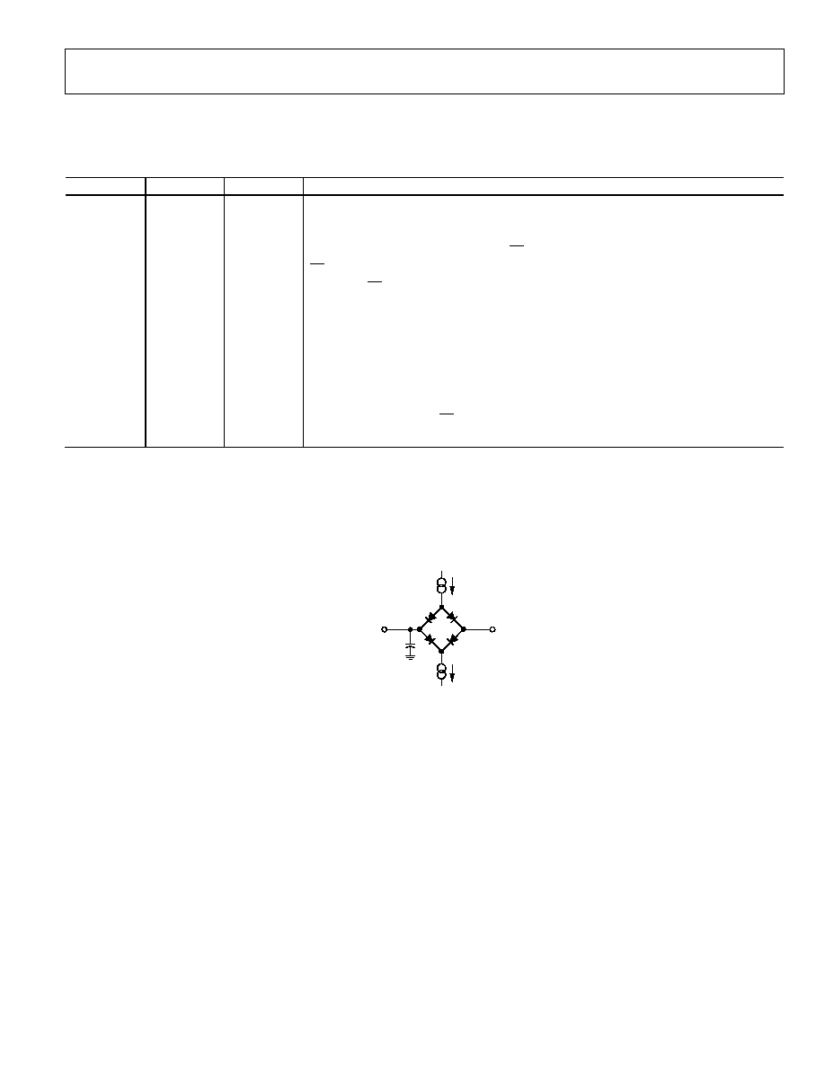
Figure 3. Load Circuit for Digital Output Timing Specifications

ADIS16100
Rev. A | Page 6 of 16
ABSOLUTE MAXIMUM RATINGS
Table 4.
Parameter Rating
Stresses above those listed under the Absolute Maximum
Ratings may cause permanent damage to the device. This is a
stress rating only; functional operation of the device at these or
any other conditions above those indicated in the operational
section of this specification is not implied. Exposure to absolute
maximum rating conditions for extended periods may affect
device reliability.
Acceleration (Any Axis, Unpowered, 0.5 ms)
2000 g
Acceleration (Any Axis, Powered, 0.5 ms)
2000 g
+V
CC
to COM
-0.3 V to +6.0 V
+V
DRIVE
to COM
-0.3 V to V
CC
+ 0.3 V
Analog Input Voltage to COM
-0.3 V to V
CC
+ 0.3 V
Digital Input Voltage to COM
-0.3 V to +7.0 V
Drops onto hard surfaces can cause shocks of greater than
2000 g and exceed the absolute maximum rating of the device.
Care should be exercised in handling to avoid damage.
Digital Output Voltage to COM
-0.3 V to V
CC
+ 0.3 V
STx Input Voltage to COM
-0.3 V to V
CC
+ 0.3 V
Operating Temperature Range
-40∞C to +85∞C
Storage Temperature Range
-65∞C to +150∞C
ESD CAUTION
ESD (electrostatic discharge) sensitive device. Electrostatic charges as high as 4000 V readily accumulate on
the human body and test equipment and can discharge without detection. Although this product features
proprietary ESD protection circuitry, permanent damage may occur on devices subjected to high energy
electrostatic discharges. Therefore, proper ESD precautions are recommended to avoid performance
degradation or loss of functionality.

ADIS16100
Rev. A | Page 7 of 16
PIN CONFIGURATION AND FUNCTION DESCRIPTIONS
05
461
-
02
0
F
I
L
T
R
A
T
E
V
D
R
I
V
E
A
I
N
1
N
C
C
S
V
C
C
S
T
1
NC = NO CONNECT
NC
DOUT
SCLK
DIN
AIN2
COM
V
REF
ST2
ADIS16100
BOTTOM
VIEW
(Not to Scale)
9
10
11
4
1
2
3
12
13
14
15
16
8
5
6
7
Figure 4. Pin Configuration
Table 5. Pin Function Descriptions
Pin No.
Mnemonic
Type
Description
1
1 DIN
I Data In. Data to be written to the control register is provided on this input and is clocked in on the
falling edge of the SCLK.
2 SCLK I Serial Clock. SCLK provides the serial clock for accessing data from the part and writing serial data
to the control registers. Also used as a clock source for the ADIS16100 conversion process.
3 DOUT O
Data Out. The data on this pin represents data being read from the control registers and is clocked
on the falling edge of the SCLK.
4 NC
No
Connect.
5
RATE
O
Buffered analog output representing the angular rate signal.
6
FILT
I
External capacitor connection to control bandwidth.
7 V
DRIVE
S
Power to SPI. The voltage supplied to this pin determines the voltage at which the serial interface
operates.
8 AIN1 I External Analog Input Channel 1. Single-ended analog input multiplexed into the on-chip track-
and-hold according to the setting of the ADD0 and ADD1 address bits.
9
AIN2
I
External Analog Input Channel 2. Single-ended analog input multiplexed into the on-chip track-
and-hold according to the setting of the ADD0 and ADD1 address bits.
10
COM
S
Common. Reference point for all circuitry in the ADIS16100.
11
V
REF
O
Precision 2.5 V Reference.
12
ST2
I
Self Test Input 2.
13
ST1
I
Self Test Input 1.
14 V
CC
S
Analog
Power.
15 NC
No
Connect.
16
CS
I
Chip Select. Active low. This input frames the serial data transfer and initiates the conversion
process.
1
I = Input; O = Output; S = Power supply.
ADIS16100
Rev. A | Page 8 of 16
TYPICAL PERFORMANCE CHARACTERISTICS
60
0
6.2
05
46
1-
00
7
SUPPLY CURRENT (mA)
P
E
RCE
NT
O
F
P
O
P
UL
A
T
I
O
N (
%
)
50
40
30
20
10
6.3
6.4
6.5
6.6
6.7
6.8
6.9
7.0
30
0
1845
05
46
1-
00
4
NULL (LSB)
PE
R
C
EN
T
O
F
PO
P
U
L
A
T
I
O
N
(%
)
25
20
15
10
5
1895
1945
1995
2045
2095
2145
2195
2245
Figure 5. Initial Null Histogram
Figure 8. Supply Current Histogram
80
0
05
46
1-
00
8
ST1 (LSB)
P
E
RCE
NT
O
F
P
O
P
UL
A
T
I
O
N (
%
)
70
60
50
40
30
20
10
≠371 ≠346 ≠321 ≠296 ≠271 ≠246 ≠221 ≠196 ≠171 ≠146 ≠121
2250
1850
4.7
5.3
05
46
1-
00
5
V
CC
(V)
N
U
L
L
L
E
VE
L (L
SB
)
2200
2150
2100
2050
2000
1950
1900
4.8
4.9
5.0
5.1
5.2
+85∞C
≠40∞C
+25∞C
Figure 9. Self Test 1 Histogram
Figure 6. Null Level vs. Supply Voltage
80
0
05
46
1-
00
9
ST2 (LSB)
P
E
RCE
NT
O
F
P
O
P
UL
A
T
I
O
N (
%
)
70
60
50
40
30
20
10
121 146 171 196 221 246 271 296 321 346 371
2040
1970
≠50
100
05
46
1-
00
6
TEMPERATURE (∞C)
N
U
L
L L
E
V
E
L (
L
S
B
)
2030
2020
2010
2000
1990
1980
≠20
10
40
70
30 PART AVERAGE, V
CC
= 4.75V
30 PART AVERAGE, V
CC
= 5V
30 PART AVERAGE, V
CC
= 5.25V
Figure 10. Self Test 2 Histogram
Figure 7. Null Level vs. Temperature
ADIS16100
Rev. A | Page 9 of 16
250
150
≠50
100
05
46
1-
0
12
TEMPERATURE (∞C)
SE
L
F
-T
ES
T
L
E
VE
L
(
L
S
B
)
240
230
220
210
200
190
180
170
160
≠20
10
40
70
30 PART AVERAGE, V
CC
= 4.75V
30 PART AVERAGE, V
CC
= 5V
30 PART AVERAGE, V
CC
= 5.25V
0
≠400
4.7
5.3
05
46
1-
0
1
1
V
CC
(V)
SE
L
F
-T
ES
T
L
EVE
L
(
L
S
B
)
≠50
≠100
≠150
≠200
≠250
≠300
≠350
4.8
4.9
5.0
5.1
5.2
+85∞C
≠40∞C
+25∞C
Figure 14. Self Test 2 vs. Temperature
Figure 11. Self Test 1 vs. Supply Voltage
3
≠3
≠50
100
05
46
1-
01
4
TEMPERATURE (∞C)
O
F
F
S
ET
L
EV
E
L
(
L
SB
)
≠20
10
40
70
2
1
0
≠1
≠2
30 PART AVERAGE, V
CC
= 4.75V
30 PART AVERAGE, V
CC
= 5V
30 PART AVERAGE, V
CC
= 5.25V
400
0
4.7
5.3
05
46
1-
01
0
V
CC
(V)
SE
L
F
-T
ES
T
L
EVE
L
(
L
S
B
)
350
300
250
200
150
100
50
4.8
4.9
5.0
5.1
5.2
+85∞C
+25∞C
≠40∞C
Figure 15. ADC Offset vs. Temperature and Supply Voltage
Figure 12. Self Test 2 vs. Supply Voltage
3
≠3
≠50
100
05
461
-
01
5
TEMPERATURE (∞C)
G
AI
N E
RRO
R (
L
S
B)
≠20
10
40
70
2
1
0
≠1
≠2
30 PART AVERAGE, V
CC
= 4.75V
30 PART AVERAGE, V
CC
= 5V
30 PART AVERAGE, V
CC
= 5.25V
≠150
≠250
≠50
100
05
461
-
01
3
TEMPERATURE (∞C)
SEL
F
-
T
EST
L
EV
E
L
(
L
SB
)
≠160
≠170
≠180
≠190
≠200
≠210
≠220
≠230
≠240
≠20
10
40
70
30 PART AVERAGE, V
CC
= 4.75V
30 PART AVERAGE, V
CC
= 5V
30 PART AVERAGE, V
CC
= 5.25V
Figure 16. ADC Gain Error vs. Temperature (Excluding V
REF
)
Figure 13. Self Test 1 vs. Temperature

ADIS16100
Rev. A | Page 10 of 16
2060
0
05
46
1
-
01
7
XXX
(X
)
2055
2050
2045
2040
1000
2000
3000
4000
5000
6000
7000
8000
000001111111011X
000001111111100X
000001111111101X
000001111111110X
000001111111111X
000010000000000X
000010000000001X
000010000000010X
0000100000000 11X
000010000000100X
000010000000101X
000010000000 110X
1
0
5
9
339
1307
4132
1996
387
12
3
1
SAMPLES = 8192, SPREAD = 23, STD DEV = 1.695,
MEAN = 2050.682
2.500
2.490
4.7
5.3
05
46
1-
01
6
V
CC
(V)
V
RE
F
LE
V
E
L
(
V
)
2.499
2.498
2.497
2.496
2.495
2.494
2.493
2.492
2.491
4.8
4.9
5.0
5.1
5.2
+85∞C
+25∞C
≠40∞C
Figure 17. V
REF
vs. Supply Voltage
Figure 18. Noise Histogram

ADIS16100
Rev. A | Page 11 of 16
THEORY OF OPERATION
The ADIS16100 operates on the principle of a resonator gyro.
Two polysilicon sensing structures each contain a dither frame,
which is electrostatically driven to resonance. This produces the
necessary velocity element to produce a Coriolis force during
angular rate. At two of the outer extremes of each frame, orthogo-
nal to the dither motion, are movable fingers that are placed
between fixed pickoff fingers to form a capacitive pickoff structure
that senses Coriolis motion. The resulting signal is fed to a series
of gain and demodulation stages that produce the electrical rate
signal output. The rate signal is then converted to a digital
representation of the output on the SPI pins. The dual-sensor
design rejects external g-forces and vibration. Fabricating the
sensor with the signal conditioning electronics preserves signal
integrity in noisy environments.
The trade-off associated with increasing the full-scale range are
potential increase in output null drift (as much as 2∞/sec over
temperature) and introducing initial null bias errors that must
be calibrated.
SETTING BANDWIDTH
The ADIS16100 provides the ability to reduce the bandwidth.
This important feature enables a simple method for achieving
optimal bandwidth/noise trade-offs. An external capacitor can
be used in combination with an on-chip resistor to create a low-
pass filter to limit the bandwidth of the ADIS16100's rate response.
The -3 dB frequency is defined as
(
)
(
)
F
0.022
2
1/
+
◊
◊
◊
=
OUT
OUT
OUT
C
R
f
The electrostatic resonator requires 14 V to 16 V for operation.
Because only 5 V is typically available in most applications, a
charge pump is included on-chip.
where R
OUT
represents an internal impedance that was trimmed
during manufacturing to 180 k ± 1%.
Any external resistor applied between the RATE pin and the
FILT pin results in
After the demodulation stage, there is a single-pole, low-pass
filter included on-chip that is used to limit high frequency
artifacts before final amplification. A second single-pole, low-
pass filter is set up via the bandwidth limit capacitor, C
OUT
. This
pole acts as the primary filter within the system (see the
(
) (
)
EXT
EXT
OUT
R
R
R
+
◊
=
k
180
/
k
180
With C
OUT
= 0 F, a default -3 dB frequency response of 40 Hz
is obtained, based upon an internal 0.022 F capacitor imple-
mented on-chip.
Increasing
Measurement Range section).
SUPPLY AND COMMON CONSIDERATIONS
SELF-TEST FUNCTION
Power supply noise and transient behaviors can influence the
accuracy and stability of any sensor-based measurement system.
When considering the power supply for the ADIS16100, it is
important to understand that the ADIS16100 provides 0.2 F of
decoupling capacitance on the V
CC
pin. Depending on the level
of noise present in the system power supply, the ADIS16100
may not require any additional decoupling capacitance for this
supply. The analog supply, V
CC
, and the digital drive supply,
V
DRIVE
, are segmented to allow multiple logic levels to be used in
receiving the digital output data. V
DRIVE
is intended for the
down-stream logic power supply and supports standard 3.3 V
and 5 V logic families. The V
DRIVE
supply does not have internal
decoupling capacitors.
The ADIS16100 includes a self-test feature that actuates each of
the sensing structures and associated electronics in the same
manner, as if subjected to angular rate. It provides a simple
method for exercising the mechanical structure of the sensor,
along with the entire signal processing circuit. It is activated by
standard logic high levels applied to Input ST1, Input ST2, or
both. ST1 causes a change in the digital output equivalent to
typically -221 LSB, and ST2 causes an opposite +221 LSB
change. The self-test response follows the viscosity temperature
dependence of the package atmosphere, approximately
0.25%/∞C.
Activating both ST1 and ST2 simultaneously is not damaging.
Because ST1 and ST2 are not necessarily closely matched,
actuating both simultaneously can result in an apparent null
bias shift.
INCREASING MEASUREMENT RANGE
The full-scale measurement range of the ADIS16100 is increased
by placing an external resistor between the RATE pin and the
FILT pin. This external resistor would be in parallel with an
internal 180 k, 1% resistor. For example, a 330 k external
resistor gives ~50% increase in the full-scale range. This is
effective for up to a 4◊ increase in the full-scale range
(minimum value of the parallel resistor allowed is 45 k). The
internal circuitry headroom requirements prevent further
increase in the linear full-scale output range.
CONTINUOUS SELF TEST
As an additional failure detection measure, power-on self test
can be performed. However, some applications warrant a
continuous self test-while-sensing rate.

ADIS16100
Rev. A | Page 12 of 16
CONTROL REGISTER
The control register on the ADIS16100 is a 12-bit, write-only
register. Data is loaded from the DIN pin on the falling edge of
SCLK. The data is transferred on the DIN line at the same time
that the conversion result is read from the part. The data
transferred on the DIN line dictates the configuration for the
next conversion. This requires 16 serial clocks for every data
transfer. Only the information provided on the first 12 falling
clock edges (after CS falling edge) is loaded to the control
register.
MSB denotes the first bit in the data stream. Table 8 shows the
analog input channel selection options.
Table 6. Channel Selection
ADD1
ADD0
Analog Input Channel
0 0 Gyroscope
0
1
Temperature sensor
1
0
AIN1 input
1
1
AIN2 input
Table 7. The DIN Bit Stream
MSB (11)
LSB (0)
WRITE LOW DONTC DONTC ADD1 ADD0 HIGH HIGH DONTC DONTC LOW CODING
Table 8. Analog Input Channel Selection Options
Bit Mnemonic Comment
11 WRITE
The value written to this bit of the control register determines whether the following 11 bits are loaded to the
control register or not. If this bit is a 1, the following 11 bits are written to the control register. If it is a 0, the
remaining 11 bits are not loaded to the control register, and it remains unchanged.
10
LOW
This bit should be held low.
9, 8
DONTC
Don't care.
7, 6
ADD1, ADD0
These two address bits are loaded at the end of the present conversion sequence and select which analog input
channel is to be converted in the next serial transfer. The selected input channel is decoded as shown in Table 6.
The address bits corresponding to the conversion result are output on DOUT prior to the 12 bits of data. The next
channel to be converted is selected by the mux on the 14th SCLK falling edge.
5, 4
HIGH
These pins should be held high.
3, 2
DONTC
Don't care.
1
LOW
This bit should be held low.
0 CODING
This bit selects the type of output coding used for the conversion result. If this bit is set to 0, the output coding for
the part is twos complement. If this bit is set to 1, the output coding from the part is straight binary (for the next
conversion).

ADIS16100
Rev. A | Page 13 of 16
SERIAL INTERFACE
During this same cycle, the digital output data is clocked out on
the DOUT pin, with the bit transitions occurring shortly after
the SCLK falling edges. The DOUT bit sequence is character-
ized in
Figure 2 shows the detailed timing diagram for the serial
interface to the ADIS16100. The chip select signal, CS, frames
the entire data transfer, because it must be kept in a Logic 0
state to communicate with the ADIS16100. The serial clock,
SCLK, provides the conversion clock and controls the transfer
of information to and from the ADIS16100 during each conver-
sion cycle. The data input, DIN, provides access to critical
control parameters in the control register, and the output signal,
DOUT, provides access to the output data of the ADIS16100.
Table 9 and Table 10. On the 16th falling edge of SCLK, the
DOUT line goes back into a three-state mode. If the rising edge of
CS occurs before 16 SCLKs have elapsed, the DOUT line goes
back into three-state mode and the control register is not updated.
Otherwise, DOUT returns to a three-state mode on the 16th
SCLK falling edge, as shown in Figure 2.
RATE SENSITIVE AXIS
This is a z-axis rate-sensing device that is also called a yaw rate
sensing device. It produces a positive going output voltage for
clockwise rotation about the axis normal to the package top,
that is, clockwise when looking down at the package lid.
The ADIS16100 offers an efficient data transfer function by
supporting simultaneous READ and WRITE cycles. A data
transfer cycle is started when the CS transitions to a Logic 0
state. If DIN is in Logic 1 state during the first falling edge of
the SCLK, then the next 11 SCLK cycles fill the control register
with the contents on the DIN pin. The appropriate bit definitions
for DIN can be found in
2.5V
RATE
AXIS
RATE
RATE IN
GND
4.75V
0.25V
LATERAL AXIS
A1
LONGITUDINAL
AXIS
V
CC
= 5V
05
46
1-
0
19
Table 7 and Table 8. If the DIN is in
a Logic 0 state during the first falling edge of the SCLK, then
contents of the control register remain unchanged. Because the
control register is only 12-bits wide, the contents on the DIN
pin during the last four SCLK cycles are ignored.
Figure 19. Rate Signal Increases with Clockwise Rotation
Table 9. DOUT Bit Stream
SCLK1
SCLK16
LOW LOW ADD1 ADD0 DB11 DB10 DB9 DB8 DB7 DB6 DB5 DB4 DB3 DB2 DB1 DB0
Table 10. DOUT Bit Functions
SCLK Mnemonic Comment
1, 2
LOW
The outputs are low for SCLK1 and SCLK2.
3, 4
ADD1, ADD0
The address bits corresponding to the conversion result are output on DOUT prior to the 12 bits of data.
See Table 6 for the coding of these address bits.
5
DB11
Data Bit 11 (MSB).
6 to 15
DB10 to DB1
Data Bit 10 to Data Bit 1.
16
DB0
Data Bit 0 (LSB).
ADIS16100
Rev. A | Page 14 of 16
SECOND-LEVEL ASSEMBLY
05
46
1-
02
2
t
P
t
L
t
25∞C TO PEAK
t
S
PREHEAT
CRITICAL ZONE
T
L
TO T
P
TE
M
P
E
R
A
T
U
R
E
TIME
RAMP-DOWN
RAMP-UP
T
SMIN
T
SMAX
T
P
T
L
The recommended pad geometries for the ADIS16100 are
displayed in Figure 20. The ADIS16100 can be attached to
printed circuit boards using Sn63 or an equivalent solder.
Figure 21 and Table 11 provide recommended solder reflow
profiles for each solder type. Note: These profiles may not be
the optimum profile for the user's application. In no case should
the temperature exceed 260∞C. It is recommended that the user
develop a reflow profile based upon the specific application.
In general, keep in mind that the lowest peak temperature and
shortest dwell time above the melt temperature of the solder
results in less shock and stress to the product. In addition,
evaluating the cooling rate and peak temperature can result in
a more reliable assembly.
Figure 21. Recommended Solder Reflow Profiles
Table 11. Solder Profile Characteristics
Profile Feature
Sn63/Pb37
6.873
2◊
0.5 BSC
16◊
0.67 BSC
12◊
1 BSC
16◊
0.9315
4◊
0.9315
4◊
05
46
1-
0
18
Average Ramp Rate (T
L
to T
P
) 3∞C/sec
max
Preheat
Minimum Temperature (T
SMIN
) 100∞C
Maximum Temperature (T
SMAX
) 150∞C
Time (T
SMIN
to T
SMAX
) (t
S
)
60 sec to 120 sec
T
SMAX
to T
L
Ramp-Up Rate
3∞C/sec
Time Maintained Above Liquidous (T
L
)
Liquidous Temperature (T
L
) 183∞C
Time (t
L
)
60 sec to 150 sec
Peak Temperature (T
P
)
240∞C + 0∞C/≠5∞C
10 sec to 30 sec
Time Within 5∞C of Actual Peak
Temperature (t
p
)
Ramp-Down Rate
6∞C/sec max
Time 25∞C to Peak Temperature
6 min max
Figure 20. Second Level Assembly Pad Layout
ADIS16100
Rev. A | Page 15 of 16
OUTLINE DIMENSIONS
TOP VIEW
SIDE VIEW
PIN 1
INDICATOR
7.00 TYP
BOTTOM VIEW
1.1585
BSC
0.373
BSC
0.227
BSC
PIN 1
INDICATOR
0.873
BSC
0.797
BSC
5.20
MAX
1
12
9
4
5
8
16
13
8.33
8.20 SQ
8.07
03
09
06
-
A
Figure 22. 16-Terminal Land Grid Array [LGA]
(CC-16-1)
Dimensions shown in millimeters
ORDERING GUIDE
Model
Temperature Range
Package Description
Package Option
ADIS16100ACC
-40∞C to +85∞C
16-Terminal Land Grid Array (LGA)
CC-16-1
ADIS16100/PCB
Evaluation
Board

ADIS16100
Rev. A | Page 16 of 16
NOTES
©2006 Analog Devices, Inc. All rights reserved. Trademarks and
registered trademarks are the property of their respective owners.
D05461-0-5/06(A)