 | –≠–ª–µ–∫—Ç—Ä–æ–Ω–Ω—ã–π –∫–æ–º–ø–æ–Ω–µ–Ω—Ç: ADIS16120 | –°–∫–∞—á–∞—Ç—å:  PDF PDF  ZIP ZIP |

Low Noise Angular Rate Sensor
Preliminary Technical Data
ADIS16120
FEATURES
Low Noise Density, .013
o
/s/
Hz, over Full Range
300
o
/sec Dynamic Range
Z-axis, yaw rate, response
Calibrated Offset and Sensitivity
320 Hz Bandwidth
External adjustment with a single component
Digital Self-Test
High Vibration Rejection
High Shock Survivability
Embedded Temperature Sensor Output
Precision Voltage Reference Output
Highly integrated, requiring minimal external components
5V single supply operation
-40
o
C to 85
o
C
APPLICATIONS
Guidance and Control
Instrumentation
Inertial measurement units
Stabilization
GENERAL DESCRIPTION
The ADIS16120 is a Low Noise and power efficient Angular
Rate Sensor (gyroscope). The circuit includes embedded signal
conditioning to provide low noise operation over the entire
300
o
/s dynamic range, as well as excellent offset and gain
accuracy over temperature. The surface-micromachining
manufacturing technology is the same high volume BIMOS
process used by Analog Devices for its high reliability
automotive airbag sensor line.
The output signal, RATE OUT, is a voltage proportional to
angular rate about the axis normal to the top surface of the
package. A precision reference and a temperature output are
available for system-level use and a digital self-test feature is
available to electromechanically excite the sensor and verify
proper operation. Variations in Range, Sensitivity, and
Bandwidth can be addressed (consult the factory).
The fully integrated design eases system implementation, and
minimizes overall power consumption to 500mW. The 36mm x
42mm (plus mounting extensions) package provides the
convenience of a standard geometry 24-pin interface and four
mounting holes.
FUNCTIONAL BLOCK DIAGRAM
Figure 1.
Rev. PrB,
4/20/2006 2:31 AM
Information furnished by Analog Devices is believed to be accurate and reliable.
However, no responsibility is assumed by Analog Devices for its use, nor for any
infringements of patents or other rights of third parties that may result from its use.
Specifications subject to change without notice. No license is granted by implication
or otherwise under any patent or patent rights of Analog Devices. Trademarks and
registered trademarks are the property of their respective owners.
One Technology Way, P.O. Box 9106, Norwood, MA 02062-9106, U.S.A.
Tel: 781.329.4700
www.analog.com
Fax: 781.326.8703
© 2006 Analog Devices, Inc. All rights reserved.

ADIS16120
Preliminary Technical Data
Rev. PrB | Page 2 of 7
TABLE OF CONTENTS
Specifications..................................................................................... 3
Absolute Maximum Ratings............................................................ 4
Rate Sensitive Axis ....................................................................... 4
ESD Caution.................................................................................. 4
Pin Configuration and Function Descriptions............................. 5
Theory of Operation ........................................................................ 6
Setting Bandwidth.........................................................................
6
Supply and Common Considerations ........................................6
Using the ADIS16120 with a Non-Ratiometric ADC ..............7
Null Adjust .....................................................................................7
Outline Dimensions ..........................................................................7
Ordering Guide .............................................................................7
REVISION HISTORY
11/16/05--PSD1 ≠ Preliminary version
1/5/06 ≠ Pr.A ≠ Preliminary Draft

Preliminary Technical Data
ADIS16120
Rev. PrB | Page 3 of 7
SPECIFICATIONS
@T
A
= 25∞C, VCC = 5 V, Angular Rate = 0∞/s, C
OUT
= 0 F, ±1 g, unless otherwise noted.
Table 1.
ADIS16120
Parameter Conditions
Min
1
Typ Max
1
Unit
SENSITIVITY Clockwise
rotation is positive output
Dynamic Range
2
Full-scale range over specifications range
±300
∞/s
Initial @25∞C
4.95
5
5.05
mV/∞/s
Over Temperature
3
V
S
= 4.75 V to 5.25 V
TBD
5
TBD
mV/∞/s
Nonlinearity
Best fit straight line
TBD
% of FS
NULL
Initial Null
2.475
2.50
2.525
V
Over Temperature
3
V
S
= 4.75 V to 5.25 V
2.45
2.55
V
Turn-On Time
Power on to ±Ω∞/s of final value, 80Hz bandwidth
4
35
ms
Linear Acceleration Effect
Any axis
TBD
∞/s/g
Voltage Sensitivity
V
CC
= 4.75 V to 5.25 V
1
∞/s/V
NOISE
PERFORMANCE
Rate Noise Density
@25∞C
0.013
∞/s/
Hz
FREQUENCY
RESPONSE
3 dB Bandwidth (User Selectable)
5
No external capacitance
320
Hz
Sensor Resonant Frequency
14
kHz
SELF-TEST
INPUTS
ST RATEOUT Response
6
ST pin from Logic 0 to 1
+150
+270
+450
mV
Logic 1 Input Voltage
Standard high logic level definition
3.3
V
Logic 0 Input Voltage
Standard low logic level definition
1.7
V
Input Impedance
To common
3.1
k
TEMPERATURE
SENSOR
V
OUT
at 298∞K
2.50
V
Max Current Load on Pin
Source to common
50
A
Scale Factor
Proportional to absolute temperature
8.4
mV/∞K
OUTPUT
DRIVE
CAPABILITY
Output Voltage Swing
I
OUT
= ±100 A
0.25
V
S
≠ 0.25
V
Capacitive Load Drive
1000
pF
2.5 V REFERENCE
Voltage Value
2.45
2.5
2.55
V
Load Drive to Ground
Source
200
A
Load Regulation
0 < I
OUT
< 200 A
5.0
mV/mA
Power Supply Rejection
4.75 V
S
to 5.25 V
S
1.0
mV/V
Temperature Drift
Delta from 25∞C
5.0
mV
POWER
SUPPLY
Operating Voltage Range
4.75
5.00
5.25
V
Quiescent Supply Current
100
132
mA
TEMPERATURE
RANGE
Specified Performance Grade A
Temperature tested to max and min specifications
≠40
+85
∞C
1
All minimum and maximum specifications are guaranteed. Typical specifications are not tested or guaranteed.
2
Dynamic range is the maximum full-scale measurement range possible, including output swing range, initial offset, sensitivity, offset drift, and sensitivity drift at
5 V supplies.
3
Specification refers to the maximum extent of this parameter as a worst-case value of T
MIN
or T
MAX
.
4
Dependent on bandwidth
5
Frequency at which response is 3 dB down from dc response with specified compensation capacitor value. Internal pole forming resistor is 180 k. See the section
titled, "SETTING THE BANDWIDTH."
6
Self-test response varies with temperature..

ADIS16120
Preliminary Technical Data
Rev. PrB | Page 4 of 7
ABSOLUTE MAXIMUM RATINGS
Table 2.
Parameter Rating
Acceleration (Any Axis, Unpowered, 0.5 ms)
2000 g
Acceleration (Any Axis, Powered, 0.5 ms)
2000 g
+V
S
≠0.3 V to +6.0 V
Output Short-Circuit Duration
(Any Pin to Common)
Indefininte
Operating Temperature Range
≠55∞C to +125∞C
Storage Temperature
≠65∞C to +150∞C
Stresses above those listed under the Absolute Maximum
Ratings may cause permanent damage to the device. This is a
stress rating only; functional operation of the device at these or
any other conditions above those indicated in the operational
section of this specification is not implied. Exposure to absolute
maximum rating conditions for extended periods may affect
device reliability.
Drops onto hard surfaces can cause shocks of greater than
2000 g and exceed the absolute maximum rating of the device.
Care should be exercised in handling to avoid damage.
RATE SENSITIVE AXIS
This is a Z-axis rate-sensing device that is also called a yaw rate
sensing device. It produces a positive going output voltage for
clockwise rotation about the axis normal to the package top, i.e.,
clockwise when looking down at the package lid.
ESD CAUTION
ESD (electrostatic discharge) sensitive device. Electrostatic charges as high as 4000 V readily accumulate on the
human body and test equipment and can discharge without detection. Although this product features
proprietary ESD protection circuitry, permanent damage may occur on devices subjected to high energy
electrostatic discharges. Therefore, proper ESD precautions are recommended to avoid performance
degradation or loss of functionality.

Preliminary Technical Data
ADIS16120
Rev. PrB | Page 5 of 7
PIN CONFIGURATION AND FUNCTION DESCRIPTIONS
Figure 2 ≠ ADIS16120 Pin Assignment (Connector-up View)
Table 3 ≠ Pin Definitions
PIN NAME
DESCRIPTION
PIN NAME
DESCRIPTION
1 ST Self
Test
2
ST Self
Test
3 ST Self
Test
4
ST Self
Test
5 ST Self
Test
6
ST Self
Test
7
ST
Self Test
8
COM
Power supply ground
9 ST
Self
Test
10
TEMPOUT
Temperature
sensor
output
11
COM
Power supply ground
12
REFOUT
Reference voltage
13
VCC
Power Supply
14
COM
Power supply ground
15
VCC
Power Supply
16
COM
Power supply ground
17
COM
Power supply ground
18
RATEOUT
Angular rate output signal
19
COM
Power supply ground
20
SUMJ
Summing Junction
21 DNC Do
not
connect
22 DNC Do
not
connect
23
COM
Power supply ground
24
DNC
Do not connect
ADIS16120
Preliminary Technical Data
Rev. PrB | Page 6 of 7
THEORY OF OPERATION
The base sensor in the ADIS16120 operates on the principle of a
resonator gyroscope. Two polysilicon sensing structures each
contain a dither frame, which is electrostatically driven to
resonance. This produces the necessary velocity element that
creates a Coriolis force during angular motion. At the two outer
extremes of each frame, orthogonal to the dither motion, are
movable fingers that are placed between fixed pickoff fingers to
form a capacitive pickoff structure that senses Coriolis motion.
The resulting signal is fed to a series of gain and demodulation
stages that produce the electrical rate signal output. One
advantage of the core dual-sensor design approach is that it
provides improved immunity against external g-forces and
vibration.
The ADIS16120 signal conditioning circuit provides an
optimized filtering network that controls the resonator's
influence on noise density while supporting a nominal
bandwidth of 320Hz. Another feature that helps reduce
sensitivity to power supply noise is the integration of
approximately 1.8uF of decoupling capacitance inside the
ADIS16120's package.
The offset and sensitivity performance is factory calibrated
across temperature and the internal reference voltage used in
this calibration process is offered for external use. A
temperature sensor is also provided for system-level use, where
appropriate.
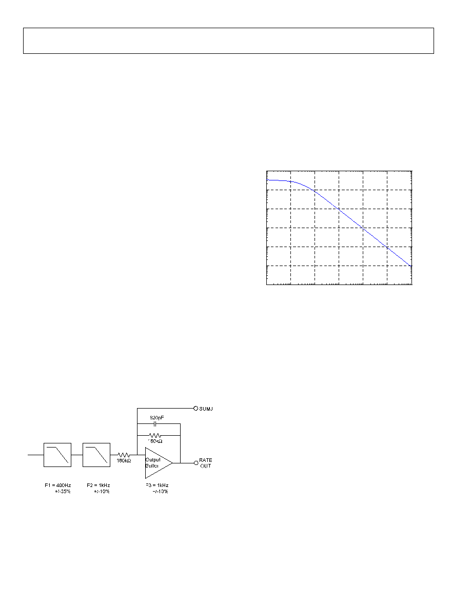
SETTING THE BANDWIDTH
An important trade-off in angular rate measurement
applications is the one between total system noise and
bandwidth. The ADIS16120 offers the flexibility to optimize
this trade-off at the system level. The ADIS16120's signal
processing circuit provides a three-pole, low pass filter, as
described in Figure 3.
Figure 3 ≠Simplified Filtering Network
The bandwidth of the third stage can be reduced by installing a
single capacitor across the RATE OUT and SUMJ pins. Figure
4 provides a relationship for selecting the appropriate capacitor
value. The initial bandwidth of the ADIS16120 is dominated by
the first stage, which is dependent on the sensor's process
variation. By reducing the bandwidth of the third filter stage,
the influence of the first stage is reduced, providing a method
for tighter bandwidth tolerances.
10
2
10
3
10
4
10
5
10
6
10
7
10
8
10
-3
10
-2
10
-1
10
0
10
1
10
2
10
3
ADIS16120 Bandwidth vs. Capacitance
Capacitance (pF)
B
and
w
i
d
t
h (
H
z
)
Figure 4 ≠ Bandwidth vs. Capacitance
SUPPLY AND COMMON CONSIDERATIONS
The ADIS16120 provides approximately 1.8uF of decoupling
capacitance internally, eliminating the need for local decoupling
capacitors in most systems.
SELF TEST FUNCTION
The ADIS16120 provides a self test function that exercises the
sensor's mechanical structure. In order to use this function,
pins 1-7 and 9 must be tied together and driven to a "high" logic
state.
USING THE ADIS16120 WITH A SUPPLY-
RATIOMETRIC ADC
The ADIS16120's RATEOUT signal is nonratiometric, i.e.,
neither the null voltage nor the rate sensitivity is proportional to
the supply. Rather they are nominally constant for dc supply
changes within the 4.75 V to 5.25 V operating range. If the
ADIS16120 is used with a supply-ratiometric ADC, the
ADIS16120's 2.5 V output can be converted and used to make
corrections in software for the supply variations.
Preliminary Technical Data
ADIS16120
Rev. PrB | Page 7 of 7
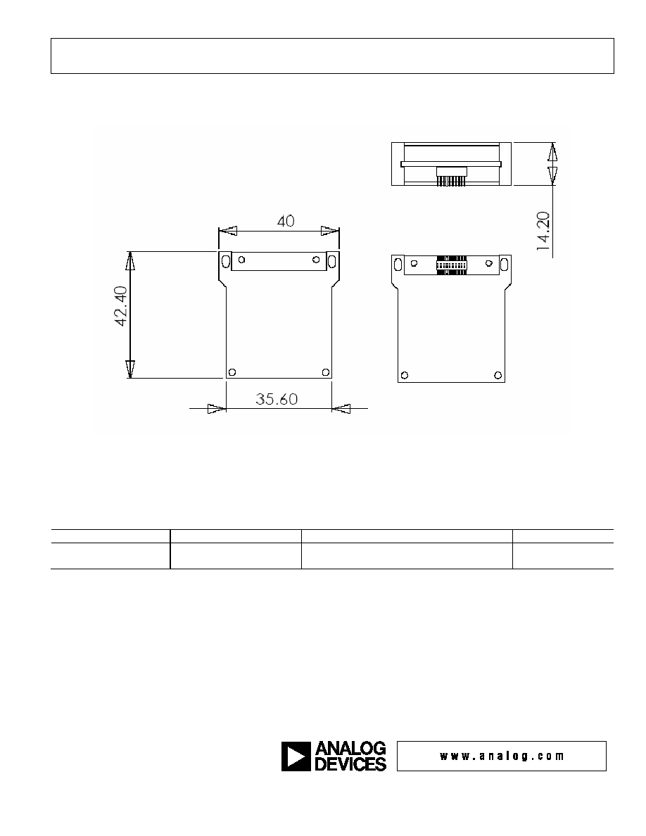
OUTLINE DIMENSIONS
Figure 5.
Dimensions shown in millimeters
ORDERING GUIDE
Model
Temperature Range
Package Description
Package Outline
ADIS16120AML
≠40∞C to +85∞C
ADIS16120/PCB
Evaluation
Board
© 2006 Analog Devices, Inc. All rights reserved. Trademarks and
registered trademarks are the property of their respective owners.
PR05923-0-4/06(PrB)