 | –≠–ª–µ–∫—Ç—Ä–æ–Ω–Ω—ã–π –∫–æ–º–ø–æ–Ω–µ–Ω—Ç: ADIS16204 | –°–∫–∞—á–∞—Ç—å:  PDF PDF  ZIP ZIP |

Programmable Dual Axis Digital
Accelerometer and Impact Sensor
Preliminary Technical Data
ADIS16204
Rev. PrA
10/10/2006 4:24 AM
Information furnished by Analog Devices is believed to be accurate and reliable. However, no
responsibility is assumed by Analog Devices for its use, nor for any infringements of patents or other
rights of third parties that may result from its use. Specifications subject to change without notice. No
license is granted by implication or otherwise under any patent or patent rights of Analog Devices.
Trademarks and registered trademarks are the property of their respective owners.
One Technology Way, P.O. Box 9106, Norwood, MA 02062-9106, U.S.A.
Tel: 781.329.4700
www.analog.com
Fax: 781.461.3113
©2006 Analog Devices, Inc. All rights reserved.
FEATURES
Dual-axis impact sensing
Dual-axis acceleration sensing, +70g, +35g
14-bit resolution
17.1 mg/LSB, 8.55mg/LSB sensitivity
Impact peak-level sample and hold
Programmable Event Recorder
400Hz double-pole Bessel sensor response
12-bit digital temperature sensor output
Digitally controlled sensitivity and bias
Digitally controlled sample rate, up to 4096 SPS
Dual alarm settings with programmable threshold limits
Auxiliary digital I/O
Digitally activated self test
Digitally activated low power mode
SPIÆ-compatible serial interface
Auxiliary 12-bit ADC input and DAC output
Single-supply operation: 3.0 V to +3.6 V
3500 g powered shock survivability
APPLICATIONS
Impact detection
Condition monitoring
Safety Systems
Shock sensor
FUNCTIONAL BLOCK DIAGRAM
Inertial
MEMS
Sensor
Self-Test
Temperature
Sensor
Signal
Conditioning
&
Conversion
Digital
Processing
Digital
Control
Aux
I/O
Alarms
Power
Management
SPI
Port
VDD
COM
AUX
DAC VREF
AUX
ADC
DIO0 DIO1
RST
CS
SCLK
DIN
DOUT
Figure 1.
GENERAL DESCRIPTION
The ADIS16204 is a programmable impact sensor in a single
compact package enabled by the Analog Devices iSensorTM
integration. By enhancing the Analog Devices iMEMSÆ sensor
technology with an embedded signal processing solution, the
ADIS16204 provides tunable digital sensor data in a convenient
format that can be accessed using a serial peripheral interface
(SPI). The SPI interface provides access to measurements for
dual-axis linear acceleration, a root-sum-square (RSS) of both
axes, temperature, power supply, and one auxiliary analog
input. Easy access to digital sensor data provides developers
with a system-ready device, reducing development time, cost,
and program risk.
Unique characteristics of the end system are accommodated
easily through several built-in features, such as a single
command in-system offset calibration, along with convenient
sample rate control.
The ADIS16204 offers the following embedded features, which
eliminate the need for external circuitry and provide a simplified
system interface:
∑
Peak sample and hold
∑
Programmable Event Recording
∑
Configurable trigger levels
∑
Auxiliary 12-bit ADC and DAC
∑
Configurable digital I/O port
∑
Digital self-test function
The ADIS16204 offers two power management features for
managing system-level power dissipation: low power mode and
a configurable shutdown feature.
The ADIS16204 is available in a 9.2 mm ◊ 9.2 mm ◊ 3.9 mm
laminate-based land grid array (LGA) package with a
temperature range of -40∞C to +105∞C.

Preliminary Technical Data
ADIS16204
Rev. PrA | Page 2 of 9
TABLE OF CONTENTS
Features .............................................................................................. 1
Applications....................................................................................... 1
Functional Block Diagram .............................................................. 1
General Description ......................................................................... 1
Revision History ............................................................................... 2
Specifications..................................................................................... 3
Timing Specifications .................................................................. 5
Timing Diagrams ..........................................................................5
Absolute Maximum Ratings ............................................................6
ESD Caution...................................................................................6
Pin Configuration and Function Descriptions..............................7
RECOMMENDED PAD GEOMETRY ..........................................7
Outline Dimensions ..........................................................................8
Ordering Guide .............................................................................8
REVISION HISTORY
8/06--Revision PSD1: PSD1 Kickoff Version

Preliminary Technical Data
ADIS16204
Rev. PrA | Page 3 of 9
SPECIFICATIONS
T
A
= -40
o
C to +105∞C, V
DD
= 3.3 V, unless otherwise noted.
Table 1.
Parameter Conditions
Axis
Min
Typ
Max
Unit
ACCELEROMETER
Output Full-Scale Range
X
+70
g
Y
+35
g
Sensitivity
X
17.1
mg/LSB
Y
8.55
mg/LSB
Non
linearity
0.2
%
Sensor-to-sensor Alignment Error
0.1
Degrees
Cross-axis
Sensitivity
-5
+5
%
Resonant
Frequency
24
kHz
OFFSET
Zero-g Output
X
0.2
g
Y
1.85
g
NOISE
Noise Density
10Hz ≠ 400Hz, no post
filtering
1.8
mg/
Hz
FREQUENCY
RESPONSE
Sensor Bandwidth (-3dB)
2-pole Bessel
360
400
440
Hz
Temperature Drift
|25∞ - Tmin| or |Tmax - 25∞C|
2
Hz
ACCELEROMETER SELF-TEST STATE
1
Output Change When Active
25∞C
X
585
LSB
Output Change When Active
Y
1170
LSB
TEMPERATURE SENSOR
Output at 25∞C
1278
LSB
Scale
Factor
-2.13
LSB/∞C
ADC
INPUT
Resolution
12
Bits
Integral
Nonlinearity
±2
LSB
Differential
Nonlinearity
±1
LSB
Offset
Error
±4
LSB
Gain
Error
±2
LSB
Input
Range
0
2.5
V
Input Capacitance
During acquisition
20
pF
ON-CHIP
VOLTAGE
REFERENCE
2.5
V
Accuracy
At
25∞C
-10
+10
mV
Reference
Temperature
Coefficient
±40
ppm/
o
C
Output
Impedance
70
DAC OUTPUT
5 k/100 pF to GND
Resolution
12
Bits
Relative Accuracy
For Code 101 to Code 4095
4
LSB
Differential
Nonlinearity
1
LSB
Offset
Error
±5
mV
Gain
Error
±0.5
%
Output Range
0 to 2.5
V
Output
Impedance
2
Output Settling Time
10
s

ADIS16204
Preliminary Technical Data
Rev. PrA | Page 4 of 9
Parameter Conditions
Axis
Min
Typ
Max
Unit
LOGIC INPUTS
Input High Voltage, V
INH
2.0
V
Input Low Voltage, V
INL
0.8
V
Logic 1 Input Current, I
INH
V
IH
= V
DD
±0.2
±1
A
Logic 0 Input Current, I
INL
V
IL
= 0 V
-40
-60
A
Input Capacitance, C
IN
10
pF
DIGITAL
OUTPUTS
Output High Voltage, V
OH
I
SOURCE
= 1.6 mA
2.4
V
Output Low Voltage, V
OL
I
SINK
= 1.6 mA
0.4
V
SLEEP
TIMER
Timeout Period
2
0.5
128
Seconds
FLASH
MEMORY
Endurance
3
20,000
Cycles
Data Retention
4
T
J
= 85∞C
20
Years
CONVERSION
RATE
Minimum
Conversion
Time
244
s
Maximum
Conversion
Time
484
ms
Maximum
Throughput
Rate
4096
SPS
Minimum
Throughput
Rate
2.066
SPS
POWER
SUPPLY
Operating Voltage Range VDD
3.0
3.3
3.6
V
Power Supply Current
Normal mode, SMPL_TIME
0x08 (f
s
910 Hz), at 25∞C
12
mA
Fast mode, SMPL_TIME
0x07
(f
s
1024 Hz), at 25∞C
37
mA
Sleep mode, at 25∞C
500
750
A
Turn-On
Time
130
ms
1
Self-test response changes as the square of V
DD
.
2
Guaranteed by design.
3
Endurance is qualified as per JEDEC Standard 22 Method A117 and measured at -40∞C, +25∞C, +85∞C, and +105∞C.
4
Retention lifetime equivalent at junction temperature (T
J
) 55∞C as per JEDEC Standard 22 Method A117. Retention lifetime decreases with junction temperature.
Preliminary Technical Data
ADIS16204
Rev. PrA | Page 5 of 9
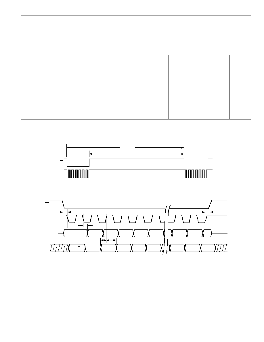
TIMING SPECIFICATIONS
T
A
= 25∞C, V
DD
= 3.3 V, tilt = 0∞, unless otherwise noted.
Table 2.
Parameter Description
Min
1
Typ Max Unit
f
SCLK
Fast mode, SMPL_TIME 0x07 (f
s
1024 Hz)
0.01
2.5
MHz
Normal mode, SMPL_TIME 0x08 (f
s
910 Hz)
0.01
1.0
MHz
t
DATARATE
Chip select period, fast mode, SMPL_TIME 0x07 (f
s
1024 Hz)
40
s
t
DATARATE
Chip select period, normal mode, SMPL_TIME 0x08 (f
s
910 Hz)
100
s
t
cs
Chip select to clock edge
48.8
ns
t
DAV
Data output valid after SCLK edge
100
ns
t
DSU
Data input setup time before SCLK rising edge
24.4
ns
t
DHD
Data input hold time after SCLK rising edge
48.8
ns
t
DF
Data output fall time
5
12.5
ns min
t
DR
Data output rise time
5
12.5
ns min
t
SFS
CS high after SCLK edge
5
ns
typ
1
Guaranteed by design, not tested.
TIMING DIAGRAMS
CS
SCLK
t
DATA RATE
t
STALL
=
t
DATA RATE
≠ 16/
f
SCLK
t
STALL
05
46
2-
00
2
Figure 2. SPI Chip Select Timing
CS
SCLK
DOUT
DIN
1
2
3
4
5
6
15
16
W/R
A5
A4
A3
A2
D2
MSB
DB14
D1
LSB
DB13
DB12
DB10
DB11
DB2
LSB
DB1
t
CS
t
SFS
t
DAV
t
DHD
t
DSU
05
46
2-
0
03
Figure 3. SPI Timing
(Utilizing SPI Settings Typically Identified as Phase = 1, Polarity = 1)
ADIS16204
Preliminary Technical Data
Rev. PrA | Page 6 of 9
ABSOLUTE MAXIMUM RATINGS
Table 3.
Parameter Rating
Acceleration (Any Axis, Unpowered)
3500 g
Acceleration (Any Axis, Powered)
3500 g
VDD to COM
-0.3 V to +7.0 V
Digital Input/Output Voltage to COM
-0.3 V to +5.5 V
Analog Inputs to COM
-0.3 to VDD + 0.3 V
Analog Inputs to COM
-0.3 to VDD + 0.3 V
Operating Temperature Range
-40∞C to +125∞C
Storage Temperature Range
-65∞C to +150∞C
Stresses above those listed under Absolute Maximum Ratings
may cause permanent damage to the device. This is a stress
rating only; functional operation of the device at these or any
other conditions above those indicated in the operational
section of this specification is not implied. Exposure to absolute
maximum rating conditions for extended periods may affect
device reliability.
Table 4. Package Characteristics
Package Type
JA
JC
Device
Weight
16-Terminal LGA
250∞C/W
25∞C/W
0.6 grams
ESD CAUTION
ESD (electrostatic discharge) sensitive device. Electrostatic charges as high as 4000 V readily accumulate on
the human body and test equipment and can discharge without detection. Although this product features
proprietary ESD protection circuitry, permanent damage may occur on devices subjected to high energy
electrostatic discharges. Therefore, proper ESD precautions are recommended to avoid performance
degradation or loss of functionality.
Preliminary Technical Data
ADIS16204
Rev. PrA | Page 7 of 9
PIN CONFIGURATION AND FUNCTION DESCRIPTIONS
ADIS16204
TOP VIEW
(NOT TO SCALE)
N/C ≠ DO NOT CONNECT
16
15
14
13
12
11
10
9
8
7
6
5
4
3
2
1
COM
N/C
N/C
RST
DIO1
VREF
VDD
AUX
DAC
DIO0
CS
DIN
DOUT
SCLK
COM
COM
AUX
ADC
Y
X
Figure 4. Pin Configuration
Table 5. Pin Function Descriptions
Pin No.
Mnemonic
Type
1
Description
1 SCLK I Serial Clock. SCLK provides the serial clock for accessing data from the part and writing serial data
to the control registers.
2 DOUT O
Data Out. The data on this pin represents data being read from the control registers and is clocked
out on the falling edge of the SCLK.
3 DIN
I Data In. Data written to the control registers is provided on this input and is clocked in on the
rising edge of the SCLK.
4
CS
I
Chip Select, Active Low. This input frames the serial data transfer.
5, 6
DIO0, DIO1
I/O
Multifunction Digital I/O Pins.
7, 11
NC
≠
No Connect.
8, 10
AUX COM
S
Auxiliary Grounds. Connect to GND for proper operation.
9
RST
I
Reset, Active Low. This input resets the embedded microcontroller to a known state.
12
AUX DAC
O
Auxiliary DAC Analog Voltage Output.
13
VDD
S
+3.3 V Power Supply.
14
AUX ADC
I
Auxiliary ADC Analog Input Voltage.
15
VREF
O
Precision Reference Output.
16
COM
S
Common. Reference point for all circuitry in the ADIS16204.
1
S = Supply; O = Output; I = Input.
RECOMMENDED PAD GEOMETRY
1.178 BSC
(8 PLCS)
0.500 BSC
(16 PLCS)
1.127 BSC
(16 PLCS)
0.670 BSC
(12 PLCS)
7.873 BSC
(2 PLCS)
05
46
2-
04
1
Figure 5. Example Pad Layout
ADIS16204
Preliminary Technical Data
Rev. PrA | Page 8 of 9
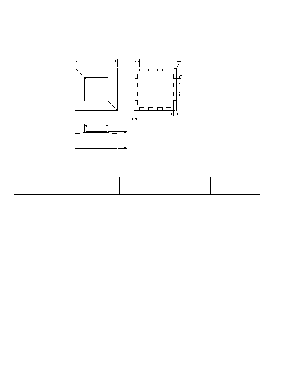
OUTLINE DIMENSIONS
03
09
06
-
A
TOP VIEW
SIDE VIEW
BOTTOM VIEW
1.405
BSC
0.373 BSC
(16 PLCS)
0.227 BSC
(4 PLCS)
A1 CORNER
INDEX AREA
1.00
BSC
0.797
BSC
3.90
MAX
1
12
9
4
5
8
16
13
9.327 MAX
SQ
5.00 TYP
Figure 6. 16-Terminal Land Grid Array [LGA]
(CC-16-2)
Dimensions shown in millimeters
ORDERING GUIDE
Model
Temperature Range
Package Description
Package Option
ADIS16204BCCZ
1
-40∞C to +105∞C
16-Terminal Land Grid Array [LGA]
CC-16-2
ADIS16204/PCBZ
Evaluation
Board
1
Z = Pb-free part.

Preliminary Technical Data
ADIS16204
Rev. PrA | Page 9 of 9
NOTES
©2006 Analog Devices, Inc. All rights reserved. Trademarks and
registered trademarks are the property of their respective owners.
PR06448-0-10/06(PrA)