 | –≠–ª–µ–∫—Ç—Ä–æ–Ω–Ω—ã–π –∫–æ–º–ø–æ–Ω–µ–Ω—Ç: ADIS16255 | –°–∫–∞—á–∞—Ç—å:  PDF PDF  ZIP ZIP |
Programmable Low Power Gyroscope
with Temperature Compensation
Preliminary Technical Data
ADIS16255
Rev. PrA
Information furnished by Analog Devices is believed to be accurate and reliable. However, no
responsibility is assumed by Analog Devices for its use, nor for any infringements of patents or other
rights of third parties that may result from its use. Specifications subject to change without notice. No
license is granted by implication or otherwise under any patent or patent rights of Analog Devices.
Trademarks and registered trademarks are the property of their respective owners.
One Technology Way, P.O. Box 9106, Norwood, MA 02062-9106, U.S.A.
Tel: 781.329.4700
www.analog.com
Fax: 781.461.3113
©2006 Analog Devices, Inc. All rights reserved.
FEATURES
Yaw rate gyro with digital range scaling
±80∞/sec, ±160∞/sec, and ±320∞/sec settings
14-bit digital gyroscope sensor outputs
12-bit digital temperature sensor output
Calibrated sensitivity and bias
Extended temperature range
In-system, auto-zero for bias drift calibration
Digitally controlled sample rate
Digitally controlled frequency response
Dual alarm settings with rate/threshold limits
Embedded integration for short-term angle estimates
Digitally activated self-test
Digitally activated low power mode
Interrupt-driven wake-up
SPIÆ-compatible serial interface
52 Hz Sensor Bandwidth
Auxiliary 12-bit ADC input and 12-bit DAC output
Auxiliary digital input/output
Single-supply operation: 4.75 V to 5.25 V
2000 g powered shock survivability
APPLICATIONS
Instrumentation control
Platform control and stabilization
Motion control and analysis
Avionics instrumentation
Navigation
Image stabilization
Robotics
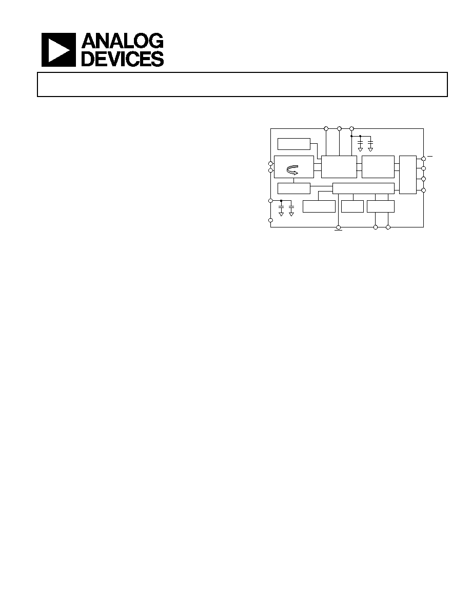
FUNCTIONAL BLOCK DIAGRAM
SCLK
DIN
DOUT
CS
RST
DIO0 DIO1
SPI
PORT
TEMPERATURE
SENSOR
SELF-TEST
POWER
MANAGEMENT
AUXILIARY
I/O
ALARM
DIGITAL
CONTROL
SIGNAL
CONDITIONING
AND
CONVERSION
CALIBRATION
AND
DIGITAL
PROCESSING
ADIS16250
VCC
FILT
RATE
COM
AUX
ADC
AUX
DAC VREF
060
70-
00
1
GYROSCOPE
SENSOR
Figure 1.
GENERAL DESCRIPTION
The ADIS16255 is a complete, angular rate measurement
system available in a single compact package enabled by Analog
Devices iSensorTM integration. By enhancing Analog Devices
iMEMSÆ sensor technology with an embedded signal processing
solution, the ADIS16255 provides factory calibrated and
tunable digital sensor data in a convenient format that can be
accessed using a simple SPI serial interface. The ADIS16255
provides calibration over an extended temperature range. The
SPI interface provides access to measurements for the gyroscope,
temperature, power supply, and one auxiliary analog input. Easy
access to calibrated digital sensor data provides developers with
a system-ready device, reducing development time, cost, and
program risk.
The device range can be digitally selected from three different
settings: ±80∞/sec, ±160∞/sec, and ±320∞/sec. Unique
characteristics of the end system are accommodated easily
through several built-in features, including a single-command
auto-zero recalibration function, as well as configurable sample
rate and frequency response. Additional features can be used to
further reduce system complexity, including:
∑
Configurable alarm function
∑
Auxiliary 12-bit ADC and DAC
∑
Two configurable digital I/O ports
∑
Digital self-test function.
System power dissipation can be optimized via the ADIS16255
power management features, including an interrupt-driven
wake-up. The ADIS16255 is available in an 11 mm ◊ 11 mm ◊
5.5 mm, laminate-based land grid array (LGA) package with a
temperature range of -40∞C to +85∞C.

ADIS16255
Preliminary Technical Data
Rev. PrA | Page 2 of 20
TABLE OF CONTENTS
Features .............................................................................................. 1
Applications....................................................................................... 1
Functional Block Diagram .............................................................. 1
General Description ......................................................................... 1
Specifications..................................................................................... 3
Timing Specifications .................................................................. 5
Absolute Maximum Ratings............................................................ 6
ESD Caution.................................................................................. 6
Pin Configuration and Function Descriptions............................. 7
Recommended Layout ..................................................................... 7
Typical Performance Characteristics ............................................. 8
Theory of Operation ........................................................................ 9
Overview........................................................................................ 9
Relative Angle Estimate ............................................................... 9
Temperature Sensor ......................................................................9
Auxiliary ADC FunctIon..............................................................9
Basic Operation .............................................................................. 10
Serial Peripheral Interface (SPI)............................................... 10
Data Output Register Access .................................................... 11
Programming and Control............................................................ 13
Control Register Overview ....................................................... 13
Control Register Access............................................................. 13
Calibration................................................................................... 13
Global Commands ..................................................................... 14
Operational Control................................................................... 15
Status and Diagnostics............................................................... 16
Outline Dimensions ....................................................................... 19
Ordering Guide .......................................................................... 19
REVISION HISTORY
10/06--Revision PrA: Pre-release

Preliminary Technical Data
ADIS16255
Rev. PrA | Page 3 of 20
SPECIFICATIONS
T
A
= -40∞C to +85∞C, V
CC
= 5.0 V, angular rate = 0∞/sec, ±1 g, ±320∞/sec range setting, unless otherwise noted.
Table 1.
Parameter Conditions
Min
Typ
Max
Unit
SENSITIVITY
Clockwise rotation is positive output
Initial
25∞C, dynamic range = ±320∞/sec
1
0.07326
degrees/sec/LSB
25∞C, dynamic range = ±160∞/sec
0.03663
degrees/sec/LSB
25∞C, dynamic range = ±80∞/sec
0.01832
degrees/sec/LSB
Tolerance
25∞C, dynamic range = ±320∞/sec
-1
+1
%
Nonlinearity
Best fit straight line
0.1
% of FS
BIAS
In Run Bias Stability
25∞C, 1
0.016
degrees/sec
Turn on--Turn on Bias Stability
25∞C, 1
0.035
degrees/sec
Angular Random Walk
25∞C, 1
3.6
o
/
hr
Linear Acceleration Effect
Any axis
0.2
degrees/sec /g
Voltage Sensitivity
V
CC
= 4.75 V to 5.25 V
1.0
degrees/sec/V
NOISE PERFORMANCE
Output Noise
At 25∞C, ±320∞/sec dynamic range, no filtering
TBD
degrees/sec
rms
At 25∞C, ±160∞/sec dynamic range, minimum
four tap filter setting
TBD
degrees/sec
rms
At 25∞C, ±80∞/sec dynamic range, minimum 16
tap filter setting
TBD
degrees/sec
rms
Rate Noise Density
At 25∞C, f = 25 Hz, no average
0.05
degrees/sec/Hz
rms
FREQUENCY RESPONSE
3 dB Bandwidth
See Analog Bandwidth section for adjustment
52
Hz
Sensor Resonant Frequency
14
kHz
Turn-on Time
Power on from SLEEP mode to ±2
degrees/sec
of final, no averaging, minimum sample period
TBD
ms
SELF-TEST STATE
Change for positive stimulus
Relative to output prior to self test
439
721
1092
LSB
Change for negative stimulus
Relative to output prior to self test
-439
-721
-1092
LSB
TEMPERATURE SENSOR
Output at 25∞C
0
LSB
Scale Factor
6.88
LSB/∞C
ADC INPUT
Resolution
12
Bits
Integral Nonlinearity
±2
LSB
Differential Nonlinearity
±1
LSB
Offset Error
±4
LSB
Gain Error
±2
LSB
Input Range
0
2.5
V
Input Capacitance
During acquisition
20
pF
ON-CHIP VOLTAGE REFERENCE
2.5
V
Accuracy At
25∞C
-10
+10
mV
Reference Temperature
Coefficient
±40
ppm/
o
K
Output Impedance
70

ADIS16255
Preliminary Technical Data
Rev. PrA | Page 4 of 20
DAC OUTPUT
5 k/100 pF to GND
Resolution
12
Bits
Relative Accuracy
For Code 101 to Code 4095
4
LSB
Differential Nonlinearity
1
LSB
Offset Error
±5
mV
Gain Error
±0.5
%
Output Range
0 to 2.5
V
Output Impedance
2
Output Settling Time
10
s
LOGIC INPUTS
Input High Voltage, V
INH
2.0
V
Input Low Voltage, V
INL
0.8
V
For CS signal when used to wake up from
SLEEP mode
0.55
V
Logic 1 Input Current, I
INH
V
IH
= 3.3 V
±0.2
±10
A
Logic 0 Input Current, I
INL
V
IL
= 0 V
40
60
A
Logic 0 Output Current (RST )
2
1
mA
Input Capacitance, C
IN
10
pF
DIGITAL OUTPUTS
Output High Voltage, V
OH
I
SOURCE
= 1.6 mA
2.4
V
Output Low Voltage, V
OL
I
SINK
= 1.6 mA
0.4
V
SLEEP TIMER
Timeout Period
3
0.5
128
Sec
FLASH MEMORY
Endurance
4
20,000
Cycles
Data Retention
5
T
J
= 55∞C
20
Years
CONVERSION RATE
Minimum Conversion Time
3.906
ms
Maximum Conversion Time
7.75
Sec
Maximum Throughput Rate
256
SPS
Minimum Throughput Rate
0.129
SPS
POWER SUPPLY
Operating Voltage Range V
CC
4.75 5.0 5.25 V
Power Supply Current
Normal mode at 25∞C
15
19
mA
Fast mode at 25∞C
41
48
mA
Sleep mode at 25∞C
500
750
A
1
The sensor is capable of +600 ∞/sec but the specifications herein are for +320∞/sec only.
2
The RST pin has an internal pull-up
3
Guaranteed by design.
4
Endurance is qualified as per JEDEC Standard 22 Method A117 and measured at -40∞C, +25∞C, +85∞C, and +125∞C.
5
Retention lifetime equivalent at junction temperature (T
J
) 55∞C as per JEDEC Standard 22 Method A117. Retention lifetime decreases with junction temperature.
Preliminary Technical Data
ADIS16255
Rev. PrA | Page 5 of 20
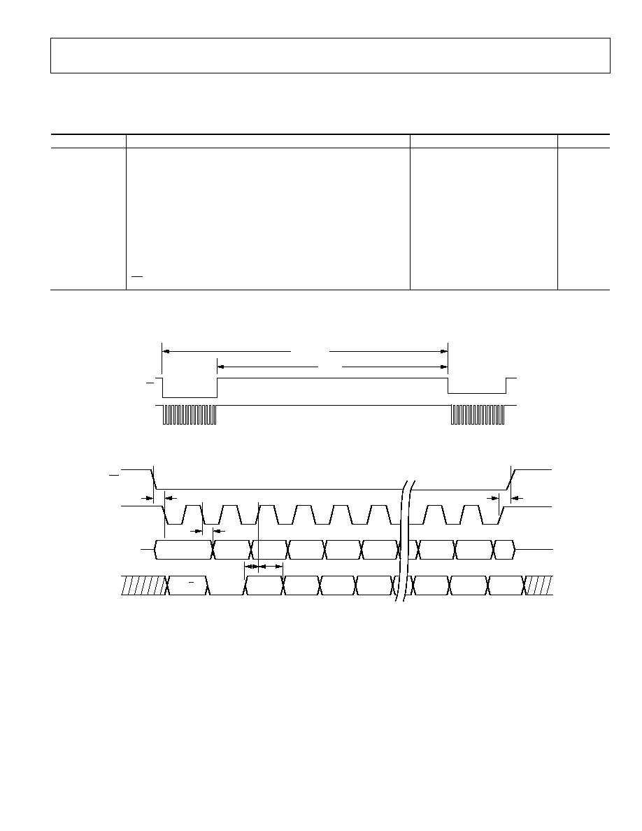
TIMING SPECIFICATIONS
T
A
= -40∞C to +85∞C, V
CC
= 5.0 V, unless otherwise noted.
Table 2.
Parameter Description
Min
1
Typ
Max
1
Unit
f
SCLK
Fast
mode
2
0.01
2.5
MHz
Normal
mode
2
0.01
1.0
MHz
t
DATARATE
Chip select period, fast mode
3
40
s
t
DATARATE
Chip select period, normal mode
3
100
s
t
cs
Chip select to clock edge
48.8
ns
t
DAV
Data output valid after SCLK edge
100
ns
t
DSU
Data input setup time before SCLK rising edge
24.4
ns
t
DHD
Data input hold time after SCLK rising edge
48.8
ns
t
DF
Data output fall time
5
12.5
ns min
t
DR
Data output rise time
5
12.5
ns min
t
SFS
CS high after SCLK edge
5
ns
typ
1
Guaranteed by design, typical specifications are not tested or guaranteed.
2
Based upon sample rate selection.
3
This number can be used to calculate t
STALL
number in Figure 2
CS
SCLK
t
DATA RATE
t
STALL
0
60
70
-
0
02
Figure 2. SPI Chip Select Timing
CS
SCLK
DOUT
DIN
1
2
3
4
5
6
15
16
W/R
A5
A4
A3
A2
D2
MSB
DB14
D1
LSB
DB13
DB12
DB10
DB11
DB2
LSB
DB1
t
CS
t
SFS
t
DAV
t
DHD
t
DSU
06
07
0-
0
03
Figure 3. SPI Timing
(Utilizing SPI Settings Typically Identified as Phase = 1, Polarity = 1)

ADIS16255
Preliminary Technical Data
Rev. PrA | Page 6 of 20
ABSOLUTE MAXIMUM RATINGS
Table 3.
Parameter Rating
Acceleration (Any Axis, Unpowered, 0.5 ms)
2000 g
Acceleration (Any Axis, Powered, 0.5 ms)
2000 g
V
CC
to COM
-0.3 V to +6.0 V
Digital Input/Output Voltage to COM
-0.3 V to +5.5 V
Analog Inputs to COM
-0.3 V to +3.5 V
Operating Temperature Range
1
-40∞C to +125∞C
Storage Temperature Range
1
-65∞C to +150∞C
1
Extended exposure to temperatures outside of the specified temperature
range of -40∞C to +85∞C can adversely affect the accuracy of the factory
calibration. For best accuracy, store the parts within the specified operating
range of -40∞C to +85∞C.
Stresses above those listed under Absolute Maximum Ratings
may cause permanent damage to the device. This is a stress
rating only; functional operation of the device at these or any
other conditions above those indicated in the operational
section of this specification is not implied. Exposure to absolute
maximum rating conditions for extended periods may affect
device reliability.
RATEOUT
RATE IN
+8.91 LSB
≠8.91 LSB
1
5 6
10
LONGITUDINAL
AXIS
0
607
0-
0
11
CLOCK-WISE
ROTATION
RATE
AXIS
LATERAL
AXIS
Figure 4. RATE OUT Level Increase with Clockwise Rotation Increase
ESD CAUTION
ESD (electrostatic discharge) sensitive device. Electrostatic charges as high as 4000 V readily accumulate on
the human body and test equipment and can discharge without detection. Although this product features
proprietary ESD protection circuitry, permanent damage may occur on devices subjected to high energy
electrostatic discharges. Therefore, proper ESD precautions are recommended to avoid performance
degradation or loss of functionality.
Preliminary Technical Data
ADIS16255
Rev. PrA | Page 7 of 20
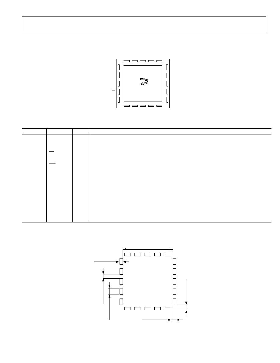
PIN CONFIGURATION AND FUNCTION DESCRIPTIONS
DNC = DO NOT CONNECT
20
19
18
17
16
15
14
13
12
11
10
9
8
7
6
5
4
3
2
1
DNC
COM
DNC
DNC
DIO1 RST
VREF
COM VCC VCC
DNC
AUX
DAC
AUX
ADC
RATE
FILT
DIO0
CS
DIN
DOUT
SCLK
POSITIVE OUTPUT
ROTATIONAL
DIRECTION
ADIS16250
TOP VIEW
(Not To Scale)
06
07
0-
00
4
Figure 5. Pin Configuration
Table 4. Pin Function Descriptions
Pin No.
Mnemonic
Type
1
Description
1
SCLK
I
SPI, Serial Clock.
2
DOUT
O
SPI, Data Output.
3
DIN
I
SPI, Data Input.
4
CS
I
SPI, Chip Select, Active Low.
5, 6
DIO0, DIO1
I/O
Multifunction Digital Input/Output Pin.
7
RST
I
Reset, Active Low. This resets the sensor signal conditioning circuit and initiates a start-up sequence.
8, 9, 10, 11
DNC
≠
Do Not Connect.
12
AUX DAC
O
Auxiliary DAC Analog Output Voltage.
13
AUX ADC
I
Auxiliary ADC Analog Input Voltage.
14
RATE
O
Analog Rate Signal Output (uncalibrated).
15 FILT I
Analog Amplifier Summing Junction. This is used for setting the analog bandwidth. See
Analog Bandwidth section for more details.
16, 17
V
CC
S
5.0 V Power Supply.
18, 19
COM
S
Common. Reference point for all circuitry in the ADIS16255.
20 V
REF
O
Precision Reference Output.
1
S = supply; O = output; I = input.
RECOMMENDED LAYOUT
0.500 BSC 2◊
9.673 BSC 20◊
0
.
773 BS
C 16◊
1.
127
BS
C 20◊
0.973 BSC 4◊
0.
973 BS
C 4◊
07
06
0-
0
10
Figure 6. Recommended Pad Layout

ADIS16255
Preliminary Technical Data
Rev. PrA | Page 8 of 20
TYPICAL PERFORMANCE CHARACTERISTICS
Figure 7.
Figure 8.
Figure 9.
.
Figure 10.
Figure 11.
Figure 12.

Preliminary Technical Data
ADIS16255
Rev. PrA | Page 9 of 20
THEORY OF OPERATION
OVERVIEW
The core angular rate sensor integrated inside the ADIS16255
is based on Analog Devices iMEMS technology. This sensor
operates on the principle of a resonator gyro. Two polysilicon
sensing structures each contain a dither frame, which is
electrostatically driven to resonance. This produces the
necessary velocity element to produce a Coriolis force during
rotation. At two of the outer extremes of each frame, orthogonal
to the dither motion, are movable fingers that are placed
between fixed fingers to form a capacitive pickoff structure that
senses Coriolis motion. The resulting signal is fed to a series of
gain and demodulation stages that produce the electrical rate
signal output.
The base sensor output signal is sampled using an ADC, and then
the digital data is fed into a proprietary digital calibration circuit.
This circuit contains calibration coefficients from the factory
calibration, along with user-defined calibration registers that can
be used to calibrate system-level errors.
The calibrated gyro data (GYRO_OUT) is made available
through output data registers along with temperature, power
supply, auxiliary ADC, and relative angle output calculations.
RELATIVE ANGLE ESTIMATE
The ANGL_OUT register offers the integration of the
GYRO_OUT data. In order for this information to be useful,
the reference angle must be known. This can be accomplished
by reading the register contents at the initial time, before
starting the monitoring, or by setting its contents to zero. This
number is reset to zero when the NULL command is used, after
a RESET command is used, and during power-up. This function
can be used to estimate change in angle over a period. The user
is cautioned to fully understand the stability requirements and
the time period over which to use this estimated relative angle
position.
TEMPERATURE SENSOR
An internal temperature sensor monitors the sensor's junction
temperature. The TEMP_OUT data register provides a digital
representation of this measurement. This sensor provides
a convenient temperature measurement for system-level
characterization and calibration feedback.
AUXILIARY ADC FUNCTION
The auxiliary ADC function integrates a standard 12-bit ADC
into the ADIS16255 to digitize other system-level analog
signals. The output of the ADC can be monitored through the
AUX_ADC control register, as defined in Table 6. The ADC is a
12-bit successive approximation converter. The output data is
presented in straight binary format with the full-scale range
extending from 0 V to V
REF
. A high precision, low drift, factory
calibrated 2.5 V reference is also provided.
Figure 13 shows the equivalent circuit of the analog input
structure of the ADC. The input capacitor, C1, is typically 4 pF
and can be attributed to parasitic package capacitance. The two
diodes provide ESD protection for the analog input. Care must
be taken to ensure that the analog input signals never exceed
the supply rails by more than 300 mV. This would cause these
diodes to become forward-biased and start conducting. They
can handle 10 mA without causing irreversible damage. The
resistor is a lumped component that represents the on resistance
of the switches. The value of this resistance is typically 100 .
Capacitor C2 represents the ADC sampling capacitor and is
typically 16 pF.
C2
C1
R1
VDD
D
D
06
07
0-
0
0
5
Figure 13. Equivalent Analog Input Circuit
Conversion Phase: Switch Open
Track Phase: Switch Closed
For ac applications, removing high frequency components from
the analog input signal is recommended by the use of a low-pass
filter on the analog input pin.
In applications where harmonic distortion and signal-to-noise
ratio are critical, the analog input must be driven from a low
impedance source. Large source impedances significantly affect
the ac performance of the ADC. This can necessitate the use of
an input buffer amplifier. When no input amplifier is used to drive
the analog input, the source impedance should be limited to
values lower than 1 k.
ADIS16255
Preliminary Technical Data
Rev. PrA | Page 10 of 20
BASIC OPERATION
The ADIS16255 is designed for simple integration into
industrial system designs, requiring only a 5.0 V power supply
and a 4-wire, industry standard serial peripheral interface (SPI).
All outputs and user-programmable functions are handled by a
simple register structure. Each register is 16 bits in length and
has its own unique bit map. The 16 bits in each register consist
of an upper (D8 to D15) and lower (D0 to D7) byte, each of
which has its own 6-bit address.
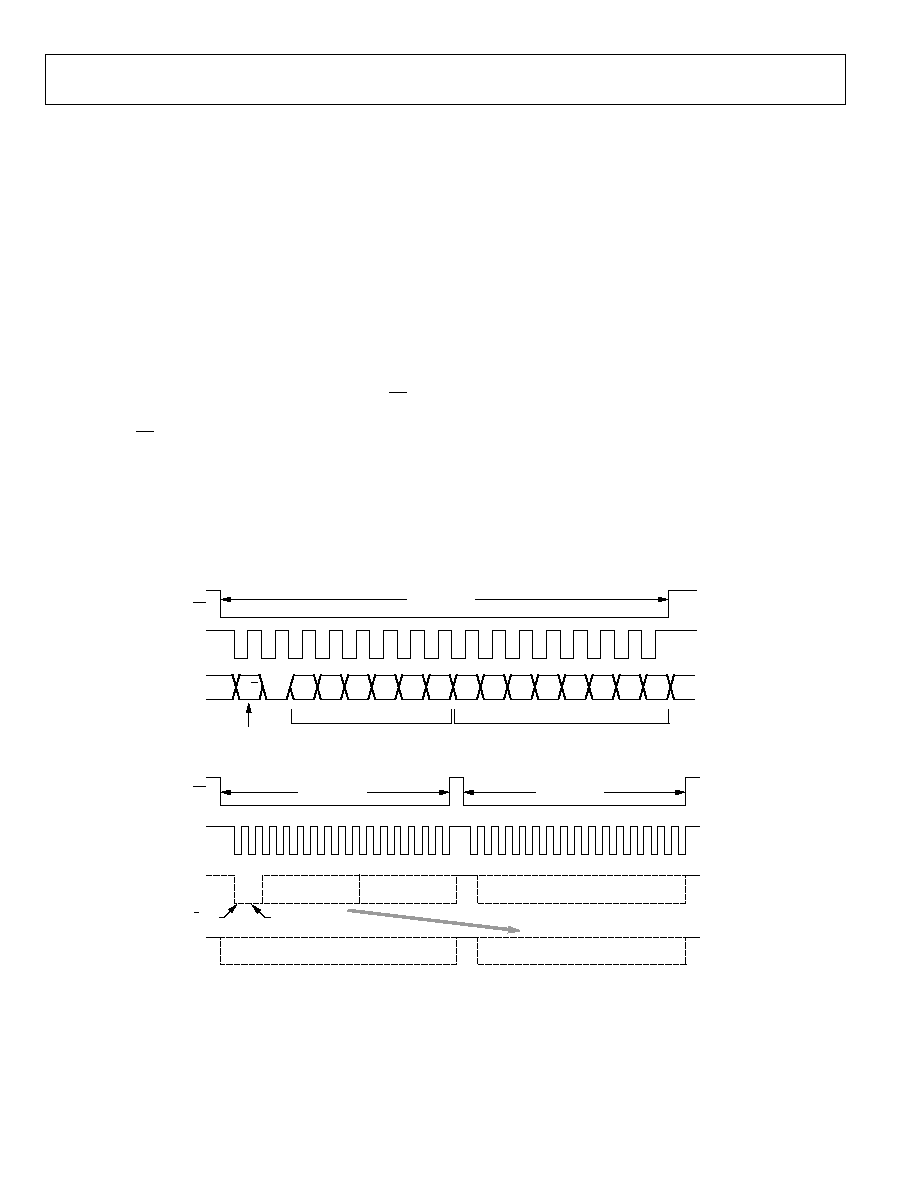
SERIAL PERIPHERAL INTERFACE (SPI)
The purpose of this section is to provide a basic description of
SPI operation in the ADIS16255. Please refer to Table 2, Figure 2,
and Figure 3 for detailed timing and operation of this port.
The ADIS16255 SPI port includes four signals: chip select (CS),
serial clock (SCLK), data input (DIN), and data output
(DOUT). The CS line enables the ADIS16255 SPI port and, in
effect, frames each SPI event. When this signal is high, the
DOUT lines are in a high impedance state, and the signals on
DIN and SCLK have no impact on operation. A complete data
frame contains 16 clock cycles. Because the SPI port operates in
full duplex mode, it supports simultaneous, 16-bit receive (DIN)
and transmit (DOUT) functions during the same data frame.
Writing to Registers
Figure 14 displays a typical data frame for writing a command
to a control register. In this case, the first bit of the DIN
sequence is a 1, followed by a 0, then the 6-bit address and
the 8-bit data command. Because each write command covers
a single byte of data, two data frames are required when writing
the entire 16-bit space of a register.
Reading from Registers
Reading the contents of a register requires a modification to the
sequence in Figure 14. In this case, the first two bits in the DIN
sequence are 0, followed by the address of the register. Each register
has two addresses (upper, lower), but either one can be used to
access its entire 16 bits of data. The final 8 bits of the DIN
sequence are irrelevant and can be counted as "don't cares"
during a read command. Then, during the next data frame, the
DOUT sequence contains the register's 16-bit data, as shown in
Figure 15. Even though a single read command requires two
separate data frames, the full duplex mode minimizes this
overhead, requiring only one extra data frame when continuously
sampling.
CS
SCLK
DIN
06
07
0-
0
06
W/R
A5
A4
A3
A2
A1
A0
DC7 DC6 DC5 DC4 DC3 DC2 DC1 DC0
DATA FRAME
WRITE = 1
READ = 0
REGISTER ADDRESS
DATA FOR WRITE COMMANDS
DON'T CARE FOR READ COMMANDS
Figure 14. DIN Bit Sequence
ADDRESS
DON'T CARE
NEXT COMMAND
BASED ON PREVIOUS COMMAND
DATA FRAME
16-BIT REGISTER CONTENTS
CS
SCLK
DIN
DOUT
W/R BIT
ZERO
06
07
0-
00
7
DATA FRAME
Figure 15. SPI Sequence for Read Commands

Preliminary Technical Data
ADIS16255
Rev. PrA | Page 11 of 20
DATA OUTPUT REGISTER ACCESS
The ADIS16255 provides access to calibrated rotation
measurements, relative angle estimates, power supply
measurements, temperature measurements, and an auxiliary
12-bit ADC channel. This output data is continuously updating
internally, regardless of user read rates. The following bit map
describes the structure of all output data registers in the
ADIS16255.
Table 5. Register Bit Map
MSB
LSB
ND EA D13 D12 D11 D10 D9 D8
D7 D6 D5 D4 D3 D2 D1 D0
The MSB holds the new data (ND) indicator. When the output
registers are updated with new data, the ND bit goes to a 1 state.
After the output data is read, it returns to a 0 state. The EA bit is
used to indicate a system error or an alarm condition that can
result from a number of conditions, such as a power supply that
is out of the specified operating range. See the Status and
Diagnostics section for more details. The output data is either
12 bits or 14 bits in length. For all of the 12-bit output data, the
D13 bit and the D12 bit are assigned "don't care" status.
The output data register map is located in
Table 6 and provides all of the necessary details for accessing
each register's data. Table 7 displays the output coding for the
GYRO_OUT register. Figure 16 provides an example SPI read
cycle for this register.
Table 6. Data Output Register Information
Name
Function
Address
Resolution (Bits)
Data Format
Scale Factor
(per LSB)
ENDURANCE
Flash Memory Write Counter 0x01,
0x00 16
Binary
N/A
SUPPLY_OUT
Power Supply Data
0◊03, 0◊02
12
Binary
1.832 mV
GYRO_OUT Gyroscope
Data
0◊05,
0◊04 14
Twos
Complement 0.07326∞/sec
1
AUX_ADC
Auxiliary Analog Input Data
0◊0B, 0◊0A
12
Binary
0.61 mV
TEMP_OUT Sensor
Temperature
Data
0◊0D, 0◊0C
12
Twos Complement
+0.1453∞C
ANGL_OUT
Angle Output
0◊0F, 0◊0E
14
Binary
0.03663∞
Table 7. Output Coding Example, GYRO_OUT
2, 3
Rate of Rotation
±320∞/sec Range
±160∞/sec Range
±80∞/sec Range
Binary Output
HEX Output
Decimal
600∞/sec
300∞/sec
150∞/sec
01 1111 1111 1111
0x1FFF
8191
320∞/sec
160∞/sec
80∞/sec
01 0001 0001 0001
0x1110
4368
80∞/sec
40∞/sec
20∞/sec
00 0100 0100 0100
0x0444
1092
40∞/sec
20∞/sec
10∞/sec
00 0010 0010 0010
0x0222
546
0.07326∞/sec
0.03663∞/sec
0.018315∞/sec
00 0000 0000 0001
0x0001
1
0∞/sec
0∞/sec
0∞/sec
00 0000 0000 0000
0x0000
0
-0.07326∞/sec
-0.03663∞/sec
-0.018315∞/sec
11 1111 1111 1111
0x3FFF
-1
-40∞/sec -20∞/sec
-10∞/sec
11 1101 1101 1110
0x3DDE
-546
-80∞/sec -40∞/sec
-20∞/sec
11 1011 1011 1100
0x3BBC
-1092
-320∞/sec -160∞/sec
-80∞/sec
10 1110 1111 0000
0x2EF0
-4368
-600∞/sec -300∞/sec
-150∞/sec
10 0000 0000 0000
0x2000
-8192
1
Assumes that the scaling is set to 320∞/sec.
2
Two MSBs have been masked off and are not considered in the coding.
3
Nominal sensitivity and zero offset null performance are assumed.

ADIS16255
Preliminary Technical Data
Rev. PrA | Page 12 of 20
CS
SCLK
DIN
DOUT
ADDRESS = 000101
DATA = 1011 1101 1101 1110
NEW DATA, NO ALARM, GYRO_OUT = ≠40∞/SECOND
W/R BIT = 0
0
706
0-
00
8
Figure 16. Example Read Cycle

Preliminary Technical Data
ADIS16255
Rev. PrA | Page 13 of 20
PROGRAMMING AND CONTROL
CONTROL REGISTER OVERVIEW
The ADIS16255 offers many programmable features that are
controlled by writing commands to the appropriate control
registers using the SPI. The following sections describe these
controls and specify each function and corresponding register
configuration. A list of features available for configuration in
this register space follows:
∑ Calibration
∑ Global commands
∑ Operational Control
∑
Sample rate
∑
Power management
∑
Digital filtering
∑
Dynamic range
∑
DAC output
∑
Digital I/O
∑ Operational Status and Diagnostics
∑
Self test
∑
Status conditions
∑
Alarms
CONTROL REGISTER ACCESS
Table 8 displays the control register map for the ADIS16255,
including address, volatile status, basic function, and
accessibility (read/write). The following sections contain
detailed descriptions and configurations for each of these
registers.
The ADIS16255 is a flash-based device with the nonvolatile
functional registers implemented as flash registers. Take into
account the endurance limitation of 20,000 writes when
considering the system-level integration of these devices. The
ENDURANCE register (see Table 30) maintains a flash memory
write count, which provides a tool for keeping track of this
limit. The nonvolatile column in Table 8 indicates the registers
that are recovered on power-up. The user must use a manual flash
update command (using the command register) to store the
nonvolatile data registers once they are configured properly.
When performing a manual flash update command, the user
needs to ensure that the power supply remains within limits for
a minimum of 50 ms after the start of the update. This ensures
a successful write of the nonvolatile data.
Table 8. Control Register Mapping
Register
Name Type Volatility
Address
Bytes Function
Reference
Table
0x10
4
Reserved
GYRO_OFF R/W
Nonvolatile
0x14
2 Gyroscope
bias offset factor
Table 9, Table 10
GYRO_SCALE R/W
Nonvolatile 0x16
2
Gyroscope scale factor
Table 11, Table 12
0x18 to to 0x1F
8
Reserved
ALM_MAG1 R/W
Nonvolatile
0x20
2 Alarm
1
amplitude threshold
Table 31, Table 32
ALM_MAG2 R/W
Nonvolatile
0x22
2 Alarm
2
amplitude threshold
Table 35, Table 36
ALM_SMPL1 R/W
Nonvolatile 0x24
2 Alarm
1 sample period
Table 33, Table 34
ALM_SMPL2 R/W
Nonvolatile 0x26
2 Alarm
2 sample period
Table 25, Table 26
ALM_CTRL R/W
Nonvolatile
0x28
2 Alarm
source control register
Table 37, Table 38
0x2A to 0x2F
6
Reserved
AUX_DAC
R/W
Volatile
0x30
2
Auxiliary DAC data
Table 21, Table 22
GPIO_CTRL
R/W
Volatile
0x32
2
Auxiliary digital I/O control register
Table 23, Table 24
MSC_CTRL R/W
Nonvolatile
1
0x34
2
Miscellaneous control register
Table 26, Table 27
SMPL_PRD
R/W
Nonvolatile
0x36
2
ADC sample period control
Table 15, Table 16
SENS/AVG R/W
Nonvolatile
0x38
2 Defines the dynamic range (sensitivity setting)
and the number of taps for the digital filter
Table 19, Table 20
SLP_CNT R/W
Volatile 0x3A
2
Counter used to determine length of power-
down mode
Table 17, Table 18
STATUS
R
Volatile
0x3C
2
System status register
Table 28, Table 29
COMMAND
W
N/A
0x3E
2
System command register
Table 13, Table 14
1
The contents of the upper byte are non-volatile and the contents of the lower byte are volatile

ADIS16255
Preliminary Technical Data
Rev. PrA | Page 14 of 20
CALIBRATION
The ADIS16255 is factory-calibrated for sensitivity and bias. It
also provides several user calibration functions for simplifying
field-level corrections. The calibration factors are stored in
nonvolatile memory and are applied using the following linear
calibration equation:
factor
scale
Offset
b
factor
scale
y
Sensitivit
m
data
n
calibratio
-
Pre
x
data
output
Calibrated
:
Where
=
=
=
=
+
=
y
b
mx
y
There are three options for system-level calibrations of the bias
in the ADIS16255: auto null, factory calibration restore, and
manual calibration updates. The auto null and factory reset
options are described in the Global Commands section.
Optional field-level calibrations use the above equation and
require two steps:
(1) characterize the behavior of the ADIS16255 at predefined
critical operating conditions, and (2) use this characterization
data to calculate and load the appropriate adjustment factors
into the GYRO_OFF ("b"). The GYRO_SCALE ("m") register
can also be adjusted to implement corrections in the sensitivity
scale factor through the system calibration process.
The GYRO_OFF provides a calibration range of ±37.5∞/sec, and
its contents are nonvolatile. The GYRO_SCALE register
provides a calibration range of 0 to 1.9995, and its contents are
nonvolatile as well.
Table 9. GYRO_OFF Register Definition
Address Scale
1
Default
Format Access
0x11,
0x10
0.018315∞/sec 0x0000 Twos
complement
R/W
1
Scale is the weight of each LSB.
Table 10. GYRO_OFF Bit Designations
Bit Description
15:12 Not
used
11:0 Data
bits
Table 11. GYRO_SCALE Register Definition
Address Scale
1
Default
2
Format
Access
0x13, 0x12
0.0488%
0x0800
Binary
R/W
1
Scale is the weight of each LSB.
2
Equates to a scale factor of one..
Table 12. GYRO_SCALE Bit Designations
Bit Description
15:12 Not
used
11:0 Data
bits
Refer to AN-879 for a detailed description of calibrating the
ADIS16255, and other MEMS gyroscopes.
GLOBAL COMMANDS
The ADIS16255 provides global commands for common
operations, such as auto null, factory calibration restore, manual
FLASH update, auxiliary DAC latch, and software reset. Each of
these global commands have a unique control bit assigned to
them in the COMMAND register and are initiated by writing a 1 to
its assigned bit.
The auto null function does two different things: it resets the
contents of the ANGL_OUT register to zero and it adjusts the
GYRO_OUT register to zero. This automated adjustment takes
twos steps: (1) read GYRO_OUT and (2) write the opposite of
this value into the GRYO_OFF register. Sensor noise influences
the accuracy of this step. For optimal calibration accuracy, set
the number of filtering taps to its maximum, wait for the
appropriate number of samples to process through the filter,
and then exercise this option.
The "factory calibration restore" command sets the contents of
GYRO_OFF to 0x0000 and GYRO_SCALE to 0x0800, erasing
any field-level calibration contents. The manual FLASH update
writes the contents of each nonvolatile register into FLASH
memory for storage. This process takes approximately 50 ms
and requires the power supply voltage to be within specification
for the duration of the event. It is worth noting that this
operation also automatically follows the auto null and factory
reset commands.
The DAC latch command loads the contents of AUX_DAC into
the DAC latches. Since the AUX_DAC contents must be
updated one byte at a time, this command ensures a stable DAC
output voltage during updates. Finally, the software reset
command sends the ADIS16255's digital processor into a re-
start sequence, effectively doing the same thing as the RST line.
Table 13. COMMAND Register Definition
Address Default Format Access
0x3F, 0x3E
N/A
N/A
Write only
Table 14. COMMAND Bit Descriptions
Bit Description
15:8 Not
used
7 Software
reset
command
6:4 Not
used
3
Manual FLASH update command
2
Auxiliary DAC data latch
1
Factory Calibration Restore command
0
Auto null command

Preliminary Technical Data
ADIS16255
Rev. PrA | Page 15 of 20
OPERATIONAL CONTROL
Internal Sample Rate
The internal sample rate defines how often data output variables
are updated, independent of the rate at which they are read out
on the SPI port. The SMPL_PRD register controls the ADIS16255
internal sample rate and has two parts: a selectable time base and
a multiplier. The sample period can be calculated using the
following equation:
( )
1
S
N
B
T
S
T
period
Sample
S
T
setting
Increment
S
N
base
Time
B
T
+
◊
=
=
=
=
The default value is the maximum 256 samples per second, and
the contents of this register are nonvolatile.
Table 15. SMPL_PRD Register Definition
Address Default Format Access
0x37, 0x36
0x0001
N/A
R/W
Table 16. SMPL_PRD Bit Descriptions
Bit Description
15:8 Not
used
7
Time base, 0 = 1.953 ms, 1 = 60.54 ms
6:0 Multiplier
Here is an example calculation of the sample period for the
ADIS16255.
(
)
SPS
T
f
ms
ms
N
T
N
B
B
ms
T
B
B
B
x
PRD
SMPL
If
S
S
S
B
S
B
64
1
624
.
15
)
1
7
(
953
.
1
1
7
0000111
0
...
6
953
.
1
0
7
00000111
0
7
,
0007
0
_
=
=
=
+
◊
=
+
◊
=
=
=
=
=
=
-
=
S
T
The sample rate setting has a direct impact on the SPI data rate
capability. For sample rates of 64 SPS and above, the SPI SCLK
can run at a rate up to 2.5 MHz. For sample rates below 64 SPS,
the SPI SCLK can run at a rate up to 1 MHz.
The sample rate setting also affects the power dissipation.
When the sample rate is set below 64 SPS, the power dissipation
reduces by a factor of 60%. The two different modes of
operation offer a system-level trade-off between performance
(sample rate, serial transfer rate) and power dissipation.
Power Management
In addition to offering two different performance modes for
power optimization, the ADIS16255 offers a programmable
shutdown period. Writing the appropriate sleep time to the
SLP_CNT register shuts the device down for the specified time.
The following example provides an illustration of this
relationship:
B7 ... B0 = 00000110
Sleep period = 3 seconds
After completing this sleep period, the ADIS16255 returns to
normal operation. If measurements are required before sleep
period completion, the ADIS16255 can be awakened by putting
the CS line in a zero logic state. Otherwise, the CS line must be
kept high to maintain sleep mode.
Table 17. SLP_CNT Register Definition
Address Scale
1
Default Format Access
0x3B, 0x3A
0.5sec
0x0000
Binary
R/W
1
Scale is the weight of each LSB.
Table 18. SLP_CNT Bit Designations
Bit Description
15:8 Not
used
7:0 Data
bits
Analog Bandwidth
The analog bandwidth of the ADIS16255 is 52 Hz. This
bandwidth can be reduced by placing an external capacitor
across the RATE and FILT pins. In this case, the analog
bandwidth can be calculated using the following equation:
f
OUT
= 1/(2 ◊ ◊ (C
OUT
+ 0.068 F))
R
OUT
= 45.22 k
C
OUT
= External capacitance
Digital Filtering
The ADIS16255 GYRO_OUT signal path has a nominal analog
bandwidth of 52 Hz. The ADIS16255 provides a Bartlett Window
FIR filter for additional noise reduction on all of the output data
registers. The SENS/AVG register stores the number of taps in
this filter in seven, power of two-step sizes (i.e. ≠2
M
= 1, 2, 4, 16,
32, 64, and 128). Filter setup requires one simple step: write the
appropriate M factor to the assigned bits in the SENS/AVG
register. The bit assignments are listed in Table 20. The following
equation offers a frequency response relationship for this filter.
(
)
(
)
s
s
A
A
B
t
f
N
t
f
N
f
H
f
H
f
H
◊
◊
◊
◊
◊
◊
=
=
sin
sin
)
(
)
(
)
(
2
0
≠160
≠140
≠120
≠100
≠80
≠60
≠40
≠20
0.001
0.01
0.1
1
07
06
0-
0
09
MA
G
N
I
T
U
D
E
(d
B
)
FREQUENCY (f/fs)
N = 128
N = 16
N = 2
N = 4
Figure 17. Bartlett Window FIR Frequency Response

ADIS16255
Preliminary Technical Data
Rev. PrA | Page 16 of 20
Dynamic Range
The ADIS16255 provides three dynamic range settings: ±80∞/sec,
±160∞/sec, and ±320∞/sec. The lower dynamic range settings
(80, 160) limit the minimum filter tap sizes in order to maintain
the resolution as the maximum rate measurements decrease.
The recommended order for programming the SENS/AVG
register is (1) dynamic range and then (2) filtering response.
The contents of the SENS/AVG register are nonvolatile.
Table 19. SENS/AVG Register Definition
Address Default Format Access
0x39, 0x38
0x0402
Binary
R/W
Table 20. SENS/AVG Bit Description
Bit Value
Description
15:11
Not
used
10:8
Sensitivity selection bits
100
320∞/sec (default condition)
010
160∞/sec, filter taps 4 (bit 3:0 0x02)
001
80∞/sec, filter taps 16 (bit 3:0 0x04)
7:4
Not
used
3:0
Filter tap setting, M = binary number
(number of taps, N = 2
M
)
Auxiliary DAC
The auxiliary DAC provides a 12-bit level adjustment function.
The AUX_DAC register controls the operation of this feature. It
offers a rail-to-rail buffered output that has a range of 0 V to 2.5 V.
The DAC can drive its output to within 5 mV of the ground
reference when it is not sinking current. As the output
approaches ground, the linearity begins to degrade (100 LSB
beginning point). As the sink current increases, the nonlinear
range increases. The DAC output latch function, contained in
the COMMAND register, provides continuous operation while
writing each byte of this register. The contents of this register
are volatile, which means that the desired output level must be
set after every reset and power cycle event.
Table 21. AUX_DAC Register Definition
Address Default
Format
Access
0x31, 0x30
0x0000
Binary
R/W
Table 22. AUX_DAC Bit Descriptions
Bit Description
15:12 Not
used
11:0 Data
bits
General Purpose I/O
The ADIS16255 provides two general-purpose pins that enable
digital I/O control using the SPI. The GPIO_CTRL control
register establishes the configuration of these pins and handles
the SPI-to-pin controls. Each pin provides the flexibility of both
input (read) and output (write) operations. For example, writing
a 0x0202 to this register establishes Line 0 as an output and set
its level as a one. Writing 0x0000 to this register establishes both
lines as inputs, and their status can be read through Bit 0 and Bit 1
of this register.
The digital I/O lines are also available for data ready and
alarm/error indications. In the event of conflict, the following
priority structure governs the digital I/O configuration:
1. GPIO_CTRL
2. MSC_CTRL
3. ALM_CTRL
Table 23. GPIO_CTRL Register Definition
Address Default Format Access
0x33, 0x32
0x0000
N/A
R/W
Table 24. GPIO_CTRL Bit Descriptions
Bit
Description
15:10 Not
used
9
General purpose I/O line 0, data direction control
1 = output, 0 = input
8
General purpose I/O line 1, data direction control
1 = output, 0 = input
7:2 Not
used
1
General purpose I/O line 0 polarity
1 = high, 0 = low
0
General purpose I/O line 1 polarity
1 = high, 0 = low
STATUS AND DIAGNOSTICS
The ADIS16255 provides a number of status and diagnostic
functions. Table 25 provides a summary of these functions,
along with their appropriate control registers.
Table 25. Status and Diagnostic Functions
Function Register
Data ready I/O indicator
MSC_CTRL
Self test, mechanical check for MEMS sensor
MSC_CTRL
Status
Check for predefined output conditions
STATUS
Flash memory endurance
ENDURANCE
Alarms
Configure and check for user-specific
conditions
ALM_MAG1/2
ALM_SMPL1/2
ALM_CTRL

Preliminary Technical Data
ADIS16255
Rev. PrA | Page 17 of 20
Data-Ready I/O Indicator
The data-ready function provides an indication of updated
output data. The MSC_CTRL control register provides the
opportunity to configure either of the general-purpose I/O pins
(DIO0 and DIO1) as a data-ready indicator signal.
Table 26. MSC_CTRL Register Definition
Address Default Format Access
0x35, 0x34
0x0000
N/A
R/W
Table 27. MSC_CTRL Bit Descriptions
Bit Description
15:11 Not
used
10
Internal self-test enable: 1 = enabled, 0 = disabled.
9
External negative rotation self-test enable
1 = enabled, 0 = disabled.
8
External positive rotation self-test enable
1 = enabled, 0 = disabled.
7:3 Not
used
2
Data-ready enable: 1 = enabled, 0 = disabled
1
Data-ready polarity: 1 = active high, 0 = active low
0
Data-ready line select:1 = DIO1, 0 = DIO0
Self Test
The MSC_CTRL register also provides a self-test function,
which verifies the MEMS sensor's mechanical integrity. There
are two different self-test options: (1) internal self-test and (2)
external self-test. The internal test provides a simple, two-step
process for checking the MEMS sensor: (1) start the process by
writing a 1 to Bit 10 in the MSC_CTRL register and (2) check
the result by reading Bit 5 of the STATUS register.
The external self-test is a static condition that can be enabled
and disabled. In this test, both positive and negative MEMS
sensor movements are available. After writing to the
appropriate control bit, the GYRO_OUT register reflects the
changes after a delay that reflects the sensor signal chain
response time. For example, the standard 52 Hz bandwidth
reflects an exponential response with a time constant of 2 ms.
The appropriate bit definitions for self-test are listed in Table 26
and Table 27.
Status Conditions
The STATUS register contains the following error-condition
flags: Alarm conditions, self-test status, angular rate over range,
SPI communication failure, control register update failure, and
power supply out of range. See Table 28 and Table 29 for the
appropriate register access and bit assignment for each flag.
The bits assigned for checking power supply range and angular
rate over range automatically reset to zero when the error
condition no longer exists. The remaining error-flag bits in the
STATUS register require a read in order to return them to zero.
Note that a STATUS register read clears all of the bits to 0.
Table 28. STATUS Register Definition
Address Default Format Access
0x3D, 0x3C
0x0000
N/A
Read only
Table 29. STATUS Bit Descriptions
Bit Description
15:10 Not
used
9
Alarm 2 status: 1 = active, 0 = inactive
8
Alarm 1 status: 1 = active, 0 = inactive
7:6 Not
used
5
Self-test diagnostic error flag
1 = error condition, 0 = normal operation
4
Angular rate over range
1 = error condition, 0 = normal operation
3
SPI communications failure
1 = error condition, 0 = normal operation
2
Control register update failed
1 = error condition, 0 = normal operation
1
Power supply in range above 5.25 V
1 = above 5.25 V, 0 = below 5.25V (normal)
0
Power supply below 4.75 V
1 = below 4.75 V, 0 = above 4.75V (normal)
Flash Memory Endurance
The ENDURANCE register maintains a running count of
writes to the Flash memory.
Table 30. ENDURANCE Register Definition
Address Default Format Access
0x01, 0x00
N/A
Binary
R
Alarms
The ADIS16255 provides two independent alarm options for
event detection. Event detections occur when output register
data meets the configured conditions. Configuration options are:
∑
All output data registers are available for monitoring
as the source data
∑
The source data can be filtered or unfiltered
∑
Comparisons can be static or dynamic (rate of change)
∑
The threshold levels and times are configurable
∑
Comparison can be greater than or less than
The ALM_MAG1 register and ALM_MAG2 register establish
the threshold level for detecting events. They take on the format
of the source data and provide a bit for establishing the greater
than/less than comparison direction. When making dynamic
comparisons, the ALM_SMPL1 register and the ALM_SMPL2
register establish the number of averages taken for the source
data as a reference for comparison. In this configuration, each
subsequent source data sample is subtracted from the previous
one, establishing an instantaneous delta.

ADIS16255
Preliminary Technical Data
Rev. PrA | Page 18 of 20
The ALM_CTRL register controls the source data selection,
static/dynamic selection, filtering selection and digital I/O
usage for the alarms.
Rate of Change Calculation
)
or
(
MSB
ALM_MAG1/2
to
according
M
with
Y
Compare
m
ChangeAlar
of
Rate
M
with
compared
be
to
Factor
Y
ALM_MAG1/2
in
comparison
for
Magnitude
M
Data
Output
Sampled
y(n)
2
ALM_SMPL1/
in
samples
of
Number
N
C
C
DS
N
1
n
C
C
C
DS
?
)
(
)
1
(
1
<
>
-
+
=
=
=
=
=
=
n
y
n
y
N
Y
DS
C
Table 31. ALM_MAG1 Register Definition
Address Default Format Access
0x21, 0x20
0x0000
N/A
R/W
The ALM_MAG1 register contains the threshold level for
Alarm 1. The contents of this register are nonvolatile.
Table 32. ALM_MAG1 Bit Designations
Bit Description
15
Comparison polarity: 1 = greater than, 0 = less than
14 Not
used
13:0
Data bits: format matches source data format
Table 33. ALM_SMPL1 Register Definition
Address Default Format Access
0x25, 0x24
0x0000
Binary
R/W
Table 34. ALM_SMPL1 Bit Designations
Bit Description
15:8 Not
used
7:0 Data
bits
Table 35. ALM_MAG2 Register Definition
Address Default Format Access
0x23, 0x22
0x0000
N/A
R/W
Table 36. ALM_MAG2 Bit Designations
Bit Description
15
Comparison polarity: 1 = greater than, 0 = less than
14 Not
used
13:0
Data bits: format matches source data format
Table 37. ALM_SMPL2 Register Definition
Address Default Format Access
0x27, 0x26
0x0000
Binary
R/W
Table 38. ALM_SMPL2 Bit Designations
Bit Description
15:8 Not
used
7:0 Data
bits
Table 39. ALM_CTRL Register Definition
Address Default Format Access
0x29, 0x28
0x0000
N/A
R/W
Table 40. ALM_CTRL Bit Designations
Bit Value
Description
15
Rate of change (ROC) enable for alarm 2
1 = rate of change, 0 = static level
14:12
Alarm 2 source selection
000 Disable
001 Power
supply
output
010 Gyroscope
output
011 Inactive
100 Inactive
101
Auxiliary ADC output
110
Temperature sensor output
111 Inactive
11
Rate of change (ROC) enable for alarm 1
1 = rate of change, 0 = static level
10:8
Alarm 1 source selection
000 Disable
001 Power
supply
output
010 Gyroscope
output
011 Inactive
100 Inactive
101
Auxiliary ADC output
110
Temperature sensor output
111 Inactive
7:5
Not
used
4
Filtered data comparison
1 = filtered data, 0 = unfiltered data
3 Not
used
2
Alarm output enable
1 = enabled, 0 = disabled
1
Alarm output polarity
1 = active high, 0 = active low
0
Alarm output line select
1 = DIO1, 0 = DIO0

Preliminary Technical Data
ADIS16255
Rev. PrA | Page 19 of 20
OUTLINE DIMENSIONS
11.127
MAX.
11.00
TYP.
11.127
MAX.
7.0
TYP.
5.5
MAX.
1
2
3
4
5
6
7
8
9
10
11
12
13
14
15
16 17 18 19
20
15
14
13
12
11
10
9
8
7
6
5
4
3
2
1
20 19 18 17 16
TOP VIEW
SIDE VIEW
BOTTOM VIEW
LAYOUT VIEW
(LOOKING THRU PART)
1.000 BSC
20 PLACES
0.900 BSC
16 PLACES
0.373 BSC
20 PLACES
1.200
BSC
1.200
BSC
PIN 1
INDICATOR
PIN 1
INDICATOR
10.173
BSC
2 PLACES
0.900 BSC
16 PLACES
0.373
BSC
20 PLACES
1.000 BSC
20 PLACES
ALL DIMENSIONS IN MM
Figure 18. 20-Terminal Land Grid Array [LGA]
(CC-20-5)
Dimensions shown in millimeters
ORDERING GUIDE
Model
Temperature Range
Package Description
Package Option
ADIS16255ACCZ
-40∞C to +85∞C
20-Terminal Land Grid Array [LGA]
CC-20-5
ADIS16255/PCBZ
Evaluation
Board

ADIS16255
Preliminary Technical Data
©2006 Analog Devices, Inc. All rights reserved. Trademarks and
registered trademarks are the property of their respective owners.
PR06462-0-10/06(PrA)
NOTES